

Page 1
User's Guide
SBOU193–July 2017
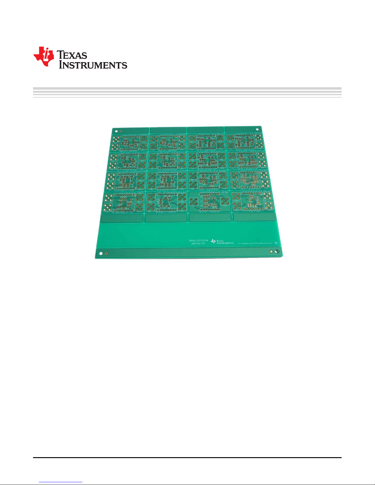
DUAL-DIYAMP-EVM
This user's guide contains support documentation for the DUAL-DIYAMP Evaluation Module (EVM).
Included is a description of how to set up and configure the EVM, printed circuit board (PCB) layout,
schematic, and bill of materials (BOM) of the DUAL-DIYAMP-EVM.
Contents
1 Introduction ................................................................................................................... 3
1.1 DUAL-DIYAMP-EVM Kit Contents................................................................................ 3
1.2 Features.............................................................................................................. 3
1.3 List of Circuits on EVM............................................................................................. 3
2 Hardware Setup.............................................................................................................. 3
2.1 EVM Circuit Locations.............................................................................................. 4
2.2 EVM Assembly Instructions ....................................................................................... 5
3 Schematic and PCB Layout ................................................................................................ 6
3.1 Schematic PCB Drawing........................................................................................... 6
3.2 Non-Inverting Amplifier............................................................................................. 7
3.3 Inverting Amplifier................................................................................................... 8
3.4 Difference Amplifier With Reference Buffer ................................................................... 10
3.5 Multiple Feedback Active Filter.................................................................................. 11
3.6 Sallen-Key Filter................................................................................................... 12
3.7 Riso With Dual-Feedback........................................................................................ 13
3.8 Two Op-Amp Instrumentation Amplifier ........................................................................ 14
3.9 Single-Ended Input to Differential Output ...................................................................... 16
3.10 Parallel Op Amps.................................................................................................. 17
3.11 Differential Input to Differential Output ......................................................................... 18
4 Connections................................................................................................................. 19
SBOU193–July 2017
Submit Documentation Feedback
Copyright © 2017, Texas Instruments Incorporated
DUAL-DIYAMP-EVM
1
Page 2

www.ti.com
4.1 Inputs and Outputs................................................................................................ 19
4.2 Power ............................................................................................................... 22
5 Bill of Materials and References ......................................................................................... 22
5.1 Bill of Materials .................................................................................................... 22
5.2 References......................................................................................................... 22
List of Figures
1 Circuit Configuration Location.............................................................................................. 4
2 Detach Desired Circuit Configuration ..................................................................................... 5
3 Detach Configuration With Attached IC and Passive Components................................................... 5
4 Terminal Strip (TS-132-G-AA) Broken Into 4-Pin Lengths ............................................................. 5
5 4-Pin Length Terminal Strips Inserted in DIP Socket................................................................... 5
6 Detached Board Configuration Position Over Terminal Pins .......................................................... 6
7 Fully-Assembled Circuit Configuration From DIYAMP-SOIC-EVM.................................................... 6
8 Silk Screen Schematic ...................................................................................................... 6
9 Non-Inverting Amplifier Schematic ........................................................................................ 7
10 Non-Inverting Amplifier Top Layer PCB Layout ......................................................................... 8
11 Inverting Amplifier Schematic .............................................................................................. 8
12 Inverting Amplifier Top Layer PCB Layout ............................................................................... 9
13 Difference Amplifier with Reference Buffer Schematic................................................................ 10
14 Difference Amplifier with Reference Buffer Top Layer PCB Layout ................................................. 11
15 Multiple Feedback Active Filter Schematic ............................................................................. 11
16 Multiple Feedback Active Filter Top Layer PCB Layout .............................................................. 12
17 Sallen-Key Active Filter Schematic ...................................................................................... 12
18 Sallen-Key Active Filter PCB Layout .................................................................................... 13
19 Riso With Dual-Feedback Schematic.................................................................................... 13
20 Riso With Dual-Feedback PCB Layout.................................................................................. 14
21 Two Op-Amp Instrumentation Amplifier Schematic.................................................................... 14
22 Two Op-Amp Instrumentation Amplifier Top Layer PCB Layout..................................................... 15
23 Single-Ended Input to Differential Output Schematic.................................................................. 16
24 Single-Ended Input to Differential Output Top Layer PCB Layout................................................... 16
25 Parallel Op Amp Schematic............................................................................................... 17
26 Parallel Op-Amp Top Layer PCB Layout................................................................................ 18
27 Differential Input to Differential Output Schematic..................................................................... 18
28 Differential Input to Differential Output Top Layer PCB Layout ...................................................... 19
29 SMA Vertical Connectors ................................................................................................. 19
30 SMA Horizontal Connectors .............................................................................................. 20
31 Wire Connections .......................................................................................................... 20
32 Through-Hole Test Points................................................................................................. 20
33 Input and Output Labeled as INA, INB and OUTA and OUTB....................................................... 21
34 Input and Output Labeled as Vin and Vout............................................................................. 21
35 Wire Alternative for Terminal Area ....................................................................................... 22
1 DUAL-DIYAMP-EVM Kit Contents ........................................................................................ 3
2 Circuit Configuration Location Legend.................................................................................... 4
3 MFB Filter Type Component Selection.................................................................................. 11
4 Sallen-Key Filter Component Type Selection .......................................................................... 12
5 DUAL-DIYAMP-EVM Bill of Materials ................................................................................... 22
2
DUAL-DIYAMP-EVM
List of Tables
Copyright © 2017, Texas Instruments Incorporated
Submit Documentation Feedback
SBOU193–July 2017
Page 3

www.ti.com
Trademarks
FilterPro is a trademark of Texas Instruments.
All other trademarks are the property of their respective owners.
1 Introduction
The DUAL-DIYAMP-EVM is an EVM developed for dual package op amps to give users the ability to
easily evaluate amplifier circuits. This “break apart” EVM has several popular op-amp configurations
including amplifiers, filters, stability compensation, and other signal conditioning circuits that require two
amplifiers. The EVM is designed for 0805 and 0603 package size surface mount components enabling
easy prototyping. This board gives the user the ability to build anything from a simple amplifier to complex
signal chains by combining different configurations.
1.1 DUAL-DIYAMP-EVM Kit Contents
Table 1 details the contents included in the DUAL-DIYAMP-EVM kit.
Table 1. DUAL-DIYAMP-EVM Kit Contents
Item Description Quantity
DUAL-DIYAMP-EVM PCB 1
Header Strip 100-mil (2.54 mm) spacing, 32 position, through hole 2
1.2 Features
The EVM has the following features:
• Multiple circuit configurations
• Breadboard compatible
• Schematic provided in silk screen on the PCB
• Multiple connector options for the input and output connections: SMA, test point, and wires.
Introduction
1.3 List of Circuits on EVM
The EVM has the following circuits:
• Non-inverting amplifier
• Inverting amplifier
• Difference amplifier with reference buffer
• Multiple feedback active filter
• Sallen-Key filter
• Riso with dual feedback
• Two op amp instrumentation amplifier
• Single-ended input to differential output
• Parallel op amps
• Differential input to differential output
2 Hardware Setup
Assembly of the DUAL-DIYAMP-EVM involves identifying and breaking out the desired circuit
configuration from the EVM, soldering the components, header strip, and input and output connections.
This section presents the details of these procedures.
SBOU193–July 2017
Submit Documentation Feedback
Copyright © 2017, Texas Instruments Incorporated
DUAL-DIYAMP-EVM
3
Page 4
A A B B
C C D D
E E F F
G H
I
J
Hardware Setup
2.1 EVM Circuit Locations
Figure 1 and Table 2 map the location of each circuit configuration on the EVM. Figure 1 labels each
circuit configuration with a letter ranging from A to J. Table 2 matches the circuit configuration to a letter in
Figure 1 and also provides the name of each individual circuit written in silk screen on the EVM.
www.ti.com
Circuit Name Silk Screen Label Letter in Figure 1
Non-inverting amplifier Non-inverting Amplifier A
Inverting amplifier Inverting Amplifier B
4
Difference amplifier with reference buffer Difference Amp C
Multiple feedback filter MFB - Filter D
Sallen-Key filter SK Filter E
Riso with dual feedback Riso Dual Feedback F
Two op amp instrumentation amplifier 2 Op Amp INA G
Single-ended input to differential output SE to Diff H
Parallel op amps Parallel Op Amps I
Differential input to differential output Diff In Diff Out J
DUAL-DIYAMP-EVM
Figure 1. Circuit Configuration Location
Table 2. Circuit Configuration Location Legend
Copyright © 2017, Texas Instruments Incorporated
SBOU193–July 2017
Submit Documentation Feedback
Page 5
www.ti.com
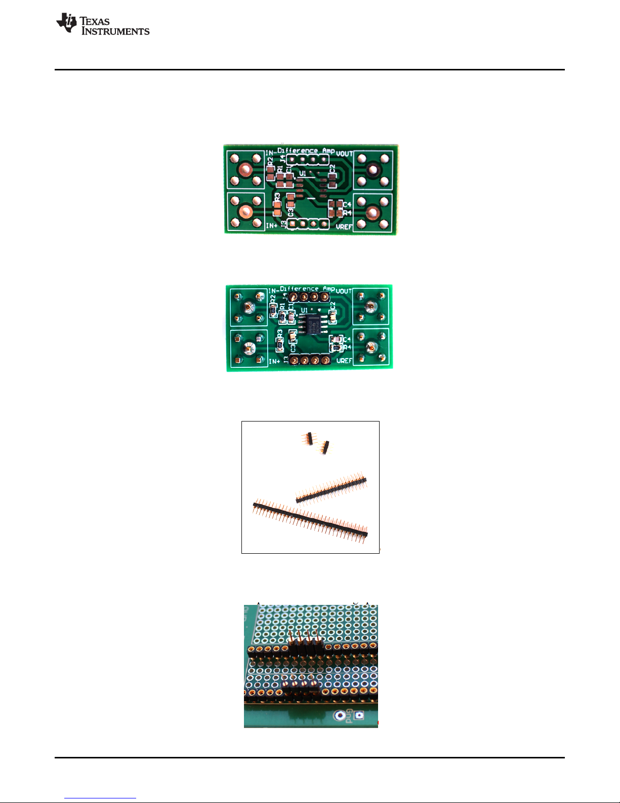
2.2 EVM Assembly Instructions
This section has step-by-step instructions on how to assemble a circuit configuration from the EVM.
1. Choose the desired circuit configuration. See Section 2.1 for the location of each circuit configuration.
2. Gently flex the PCB panel at the score lines to separate the desired circuit configuration from the EVM.
Figure 2. Detach Desired Circuit Configuration
3. Solder device and surface mount passive components to the separated PCB.
Hardware Setup
Figure 3. Detach Configuration With Attached IC and Passive Components
4. Use long-nose pliers to break header strips, provided in the EVM kit, into 8-position lengths.
Figure 4. Terminal Strip (TS-132-G-AA) Broken Into 4-Pin Lengths
5. Insert header strips into a spare DIP socket as shown in Figure 5.
Figure 5. 4-Pin Length Terminal Strips Inserted in DIP Socket
SBOU193–July 2017
Submit Documentation Feedback
Copyright © 2017, Texas Instruments Incorporated
DUAL-DIYAMP-EVM
5
Page 6
Schematic and PCB Layout
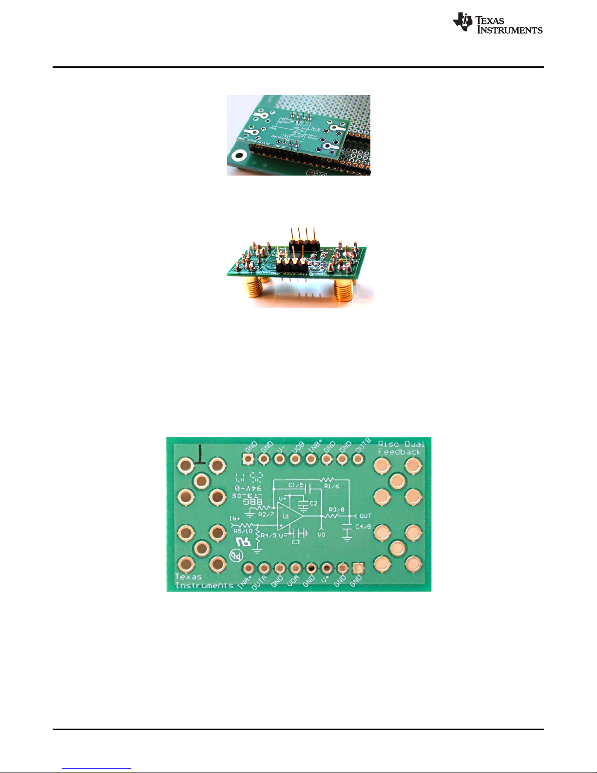
6. Position separated PCB over pins and solder the connections. Carefully remove from the DIP socket.
Figure 6. Detached Board Configuration Position Over Terminal Pins
7. Attach SMA connectors, test points, or wires to the inputs and outputs of the separated PCB.
Figure 7. Fully-Assembled Circuit Configuration From DIYAMP-SOIC-EVM
www.ti.com
3 Schematic and PCB Layout
This section provides the schematic and PCB layout of each circuit configuration provided on the EVM.
3.1 Schematic PCB Drawing
Each circuit board has the schematic of the circuit in silk screen located on the back of the PCB for easy
reference. Figure 8 displays an example of a schematic on the back of the PCB.
Figure 8. Silk Screen Schematic
6
DUAL-DIYAMP-EVM
Copyright © 2017, Texas Instruments Incorporated
Submit Documentation Feedback
SBOU193–July 2017
Page 7

c
1/4 2/6
1
2 R C
=
´ p ´ ´
f
1/4
2/ 5
R
OUTA / B 1 INA / B
R
æ ö
= +
ç ÷
è ø
+
±
C3/7
R2/5 R1/4
R3/6
C4/8
OUTA/B
INA/B
V+
C1
REFA/B
C2/6
C5
V-
www.ti.com
3.2 Non-Inverting Amplifier
Figure 9 displays the schematic for the non-inverting amplifier circuit configuration.
The non-inverting amplifier circuit configuration takes an input signal that is applied directly to the high
impedance non-inverting input and outputs a signal that is the same polarity as the input signal. The
feedback network for this topology is R1, R2, C2, and C3 for channel A and R4, R5, C6, and C7 for
channel B.
There are multiple ways to configure the non-inverting amplifier circuit configuration. The following cases
show the two primary use-case configurations for this circuit.
Case 1: Standard non-inverting circuit
This circuit can be configured into a standard non-inverting circuit by shorting C4/8 and C3/7 with a 0-Ω
resistor and leaving R3/6 unpopulated.
Equation 1 displays the transfer function of the non-inverting amplifier circuit configuration shown in
Figure 9.
Schematic and PCB Layout
Figure 9. Non-Inverting Amplifier Schematic
where
• C
• C
• R
is shorted with a 0-Ω resistor
4/8
is shorted with a 0-Ω resistor
3/7
is unpopulated (1)
3/6
Capacitor C2 for channel A and C6 for channel B provide the option to filter the output. The cutoff
frequency of the filter can be calculated using Equation 2.
Case 2: AC-coupled, non-inverting amplifier configuration
This circuit board can be configured as an ac-coupled, non-inverting circuit by populating C4/8 and C3/7
with capacitors and populating R3/6 with resistors. Test points REFA for channel A and REFB for channel
B are used to set the dc biasing of the circuit. The dc bias voltage is typically set to one half of the supply
voltage of the amplifier.
SBOU193–July 2017
Submit Documentation Feedback
Copyright © 2017, Texas Instruments Incorporated
DUAL-DIYAMP-EVM
(2)
7
Page 8
+
±
C4/7
R3/8 R2/7
R4/9
R5/10 C5/8
OUTA/B
INA/B
V+
C1
REFA/B
C3/6
R1/6
V-
C2
c
3/ 7 2/5
1
2 C R
=
´ p ´ ´
f
c
4/ 8 3 /6
1
2 C R
=
´ p ´ ´
f
Schematic and PCB Layout
Populating C4/8 with capacitors ac couples the input of the circuit. The corner frequency of the high-pass
filter created by C4/8 and R3/6 is calculated in Equation 3:
Similarly, capacitor C3/7 creates a high-pass filter with R2/5. The corner frequency of the high-pass filter
created by C3/7 and R2/5 is calculated in Equation 4.
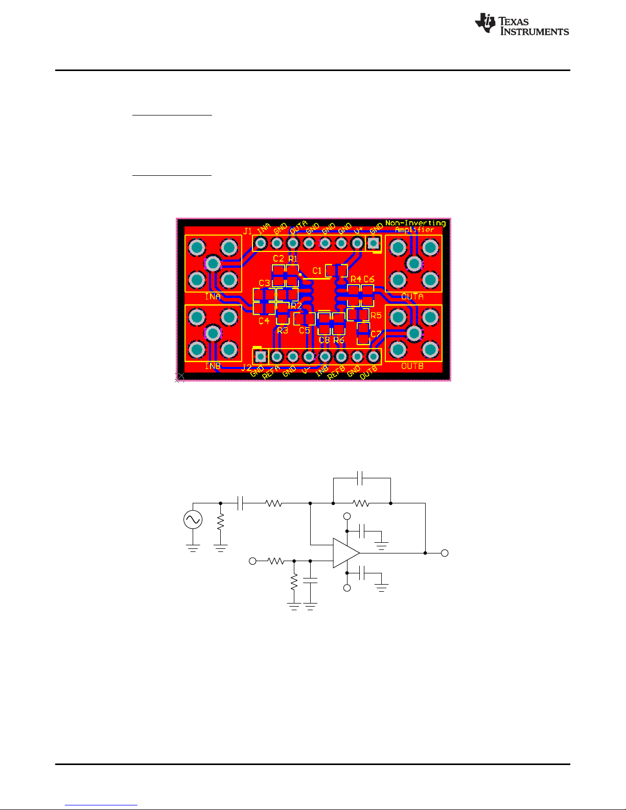
Figure 10 displays the PCB layout of the top layer of the non-inverting amplifier circuit configuration.
www.ti.com
(3)
(4)
Figure 10. Non-Inverting Amplifier Top Layer PCB Layout
3.3 Inverting Amplifier
Figure 11 shows the schematic for the inverting amplifier circuit configuration.
The inverting amplifier configuration takes an input signal and outputs a signal that is the opposite polarity
as the input signal. The benefit of this topology is that it avoids common mode limitations. The ratio of the
resistors in the feedback network will determine the amount of gain the input signal will be amplified by.
The inverting amplifier circuit configuration provides the option to ac couple the input, filter the output, and
bias the output of the amplifier to a desired value.
Figure 11. Inverting Amplifier Schematic
8
DUAL-DIYAMP-EVM
Copyright © 2017, Texas Instruments Incorporated
Submit Documentation Feedback
SBOU193–July 2017
Page 9
c _REF
5/8 4/9 5/10
1
2 C R / /R
=
´ p ´ ´
f
c _OUT
3/ 6 2/7
1
2 C R
=
´ p ´ ´
f
c _highpass
4/7 3 /8
1
2 C R
=
´ p ´ ´
f
5/10
4/ 9 5 /10
R
OUTA / B REFA / B
R R
æ ö
=
ç ÷
+
è ø
5/10
2/ 7 2/7
3/ 8 4/9 5/10 3/ 8
R
R R
OUTA / B INA / B 1 REFA / B
R R R R
æ ö æ öæ ö
= - + +
ç ÷ ç ÷ç ÷
+
è ø è øè ø
www.ti.com
Equation 5 displays the dc transfer function of the inverting amplifier circuit configuration.
Capacitor C4 for channel A and C7 for channel B provide the option to ac couple the input of the circuit.
Equation 6 displays the dc transfer function of the ac-coupled inverting amplifier circuit configuration.
Equation 7 calculates the cut-off frequency of the high-pass filter.
Capacitors C3 and C6 provide the option to filter the output. Equation 8 calculates the cut-off frequency of
the filter.
Capacitor C5 for channel A and C8 for channel B provide the option to filter noise introduced from the
reference voltage, REFA/B. Equation 9 calculates the cutoff frequency of the filter.
where
• C
is shorted with a 0-Ω resistor (5)
4/7
where
• The input is ac coupled with C
Schematic and PCB Layout
4/7
(6)
(7)
(8)
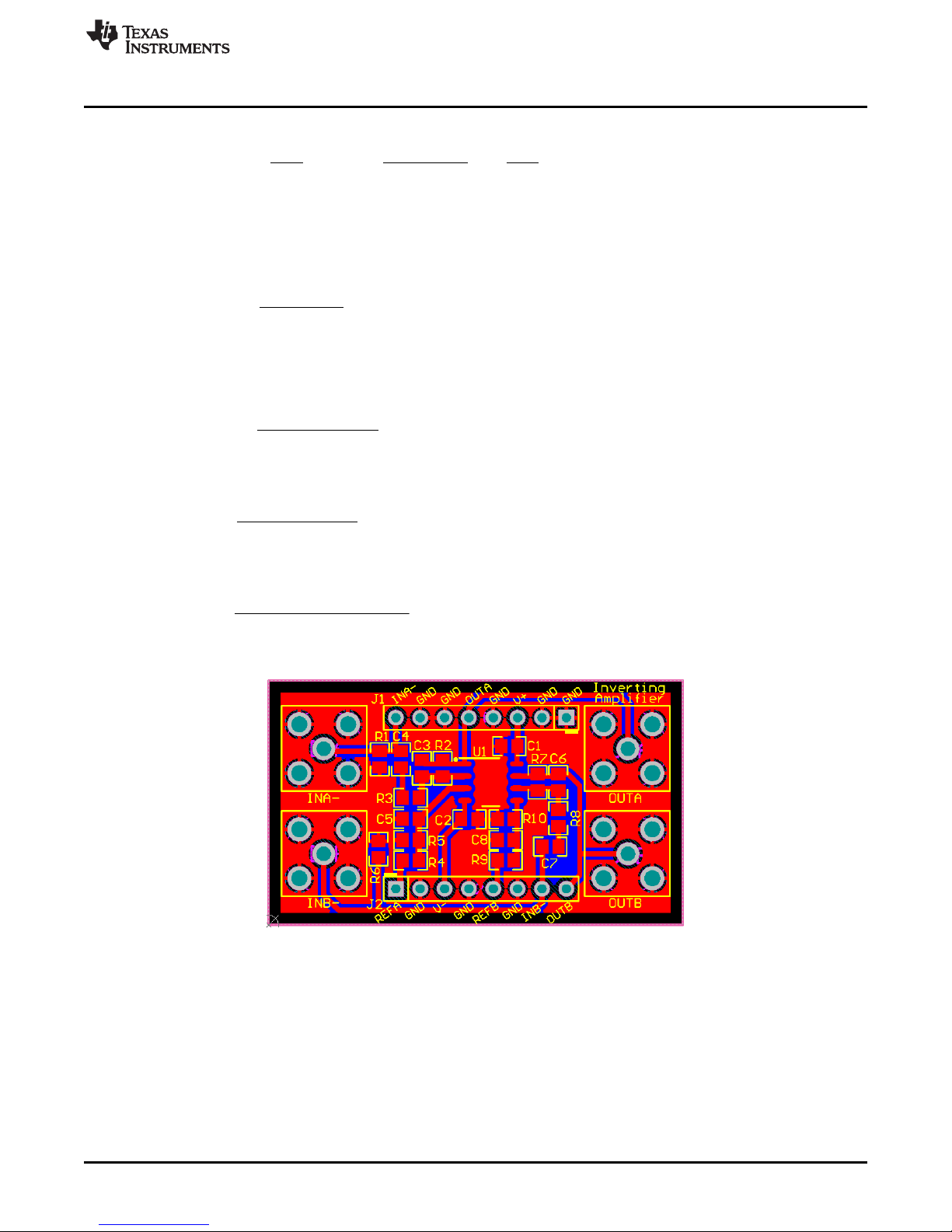
Figure 12 displays the PCB layout of the top layer of the inverting amplifier circuit configuration.
Figure 12. Inverting Amplifier Top Layer PCB Layout
(9)
SBOU193–July 2017
Submit Documentation Feedback
Copyright © 2017, Texas Instruments Incorporated
DUAL-DIYAMP-EVM
9
Page 10

c
2 1
1
2 R C
=
´ p ´ ´
f
( )
6
2
out IN IN ref
1 5 6
R
R
V V V V
R R R
+ -
æ ö
= - +
ç ÷
+
è ø
3 6
4 2 1 2
out
3 4 1 3 4 5 6 2 1
R R
R R R R
V 1 (IN ) 1 Vref (IN )
R R R R R R R R R
æ ö æ öæ ö
æ ö æ ö
= + + + + - -
ç ÷ ç ÷ç ÷
ç ÷ ç ÷
+ + +
è ø è ø
è ø è øè ø
+
±
OUT
V+
C2
C3
V-
R3
R1
C1
+
±
V-
V+
IN-
IN+
VREF
C4 R4
C6C7
R7
R2
R5
C5R6
Schematic and PCB Layout
3.4 Difference Amplifier With Reference Buffer
Figure 13 shows the schematic for the difference amplifier with reference buffer circuit configuration.
www.ti.com
Figure 13. Difference Amplifier with Reference Buffer Schematic
The difference amplifier utilizes both inverting and non-inverting inputs and produces an output that is
dependent on the difference between the inputs. The gain of the difference amplifier is dependent on the
ratio of R2 to R1 (and subsequently R4 to R3). The reference buffer in the circuit buffers the reference
voltage to maintain the common mode rejection of the difference amplifier.
Equation 10 displays the transfer function of the difference amplifier with reference buffer circuit
configuration.
If R1= R3and R2= R4, Equation 10 simplifies to Equation 11:
Capacitors C1 and C4 provide the option to filter the output of the amplifier. Equation 12 calculates the
cut-off frequency of the filter.
where
• R1= R
• R2= R
• C1= C
3
4
4
(10)
(11)
(12)
10
DUAL-DIYAMP-EVM
Copyright © 2017, Texas Instruments Incorporated
Submit Documentation Feedback
SBOU193–July 2017
Page 11

+
±
C1
Z1/6
Z4/9
Z5/10
Z3/8
Z2/7
VOUT
V+
INA/B
C3
V-
R1/3
R2/4
C2/4
REFA/B
www.ti.com
Figure 14 displays the PCB layout of the top layer of the difference amplifier with reference buffer circuit
configuration.
Figure 14. Difference Amplifier with Reference Buffer Top Layer PCB Layout
3.5 Multiple Feedback Active Filter
Figure 15 shows the schematic for the multiple feedback (MFB) active filter circuit configuration.
Schematic and PCB Layout
Figure 15. Multiple Feedback Active Filter Schematic
The MFB topology (sometimes called infinite gain or Rauch) is often preferred due to low sensitivity to
component variation. The MFB topology creates an inverting second-order stage.
The MFB filter circuit can be configured as a low-pass filter, high-pass filter, or band-pass filter based on
the component selection of Z1/6 through Z5/10. Table 3 displays the type of passive component that
should be chosen for Z1/6 through Z5/10 for each filter configuration.
Pass-Band Filter
Type
Low Pass R1/6 C2/7 R3/8 R4/9 C5/10
High Pass C1/6 R2/7 C3/8 C4/9 R5/10
Band Pass R1/6 R2/7 C3/8 C4/9 R5/10
SBOU193–July 2017
Submit Documentation Feedback
Type of
Component (Z1/6)
Table 3. MFB Filter Type Component Selection
Type of
Component (Z2/7)
Copyright © 2017, Texas Instruments Incorporated
Type of
Component (Z3/8)
Component (Z4/9)
Type of
DUAL-DIYAMP-EVM
Type of
Component (Z5/10)
11
Page 12

+
±
+
±
C1
Z1/8
Z3/10
Z5/12
Z2/9
Z4/11
OUTA/B
V+
INA/B
REFA/B
R2/4
R1/3
VBA/B
V-
C2
c _REF
2/ 4 1/3 2/4
1
2 C R / /R
=
´ p ´ ´
f
Schematic and PCB Layout
For additional guidance in designing a filter, download FilterPro™ active filter design software.
Capacitor C2 for channel A and C4 for channel B provide the option to filter noise that may be introduced
from the REFA/B. Equation 13 calculates the cut-off frequency due to C2/4.
Figure 16 displays the PCB layout of the top layer of the multiple feedback active filter circuit configuration.
Figure 16. Multiple Feedback Active Filter Top Layer PCB Layout
www.ti.com
(13)
3.6 Sallen-Key Filter
Figure 17 displays the schematic for the Sallen-Key active filter circuit configuration.
The Sallen-Key filter is one of the most commonly applied active filter topologies. The Sallen-Key filter can
be configured as a low-pass filter, high-pass filter, or band-pass filter based on the component selection of
Z1/8 through Z5/12. Table 4 displays the type of passive components that should be chosen for Z1/8
through Z5/12 for each filter configuration.
Figure 17. Sallen-Key Active Filter Schematic
Table 4. Sallen-Key Filter Component Type Selection
Pass-Band Filter
Type
12
Low Pass R1/8 R2/9 C3/10 Not Populated C5/12
High Pass C1/8 C2/9 R3/10 Not Populated R5/12
Band Pass R1/8 C2/9 R3/10 C4/11 R5/12
DUAL-DIYAMP-EVM
Type of
Component (Z1/8)
Type of
Component (Z2/9)
Copyright © 2017, Texas Instruments Incorporated
Type of
Component (Z3/10)
Type of
Component (Z4/11)
Submit Documentation Feedback
Type of
Component (Z5/12)
SBOU193–July 2017
Page 13

4/ 9 1/6
5/10 4/ 9 2/ 7
R R
OUTA / B 1 INA / B
R R R
æ ö
æ ö
= +
ç ÷
ç ÷
+
è ø
è ø
+
±
R4/9
OUTA/B
INA/B
V+
C2
C3
V-
R5/10
C4/8
R2/7
R1/6
C1/5
R3/8
www.ti.com
For guidance in designing a filter, download the FilterPro™ active filter design software.
Figure 18 displays the PCB layout of the top layer of the multiple feedback active filter circuit configuration.
Figure 18. Sallen-Key Active Filter PCB Layout
3.7 Riso With Dual-Feedback
Figure 19 displays the schematic for the Riso with dual-feedback circuit configuration.
Schematic and PCB Layout
Figure 19. Riso With Dual-Feedback Schematic
Equation 14 calculates the dc gain of the Riso with dual-feedback circuit configuration.
This capacitive load (C4/8) compensation technique uses an isolation resistor (R3/8) to compensate the
circuit by adding a zero to cancel the pole from the output impedance and capacitive load. Refer to the TI
Precision Labs - Op Amps: Stability 5 video for detailed information on this technique.
SBOU193–July 2017
Submit Documentation Feedback
Copyright © 2017, Texas Instruments Incorporated
DUAL-DIYAMP-EVM
(14)
13
Page 14

+
±
V+
C2
V-
C1
R5
C4
VREF
VIN-
R3
R4
VREF
RG
R2
+
±
V+
V-
R1
VOUT
R6
C3
VREF
VIN+
Schematic and PCB Layout
Figure 20 displays the PCB layout of the top layer of the Riso with dual-feedback circuit configuration.
Figure 20. Riso With Dual-Feedback PCB Layout
3.8 Two Op-Amp Instrumentation Amplifier
Figure 21 displays the schematic for the two op-amp instrumentation amplifier circuit configuration.
www.ti.com
14
The two op-amp instrumentation amplifier takes a differential input and outputs a single-ended signal. This
circuit configuration provides a high-impedance input to sources interfacing with this circuit. While the two
op-amp instrumentation amplifier does not provide as high of common mode rejection ration (CMRR) as
the three op-amp instrumentation amplifier topology, the two op-amp instrumentation requires only two op
amps, thereby reducing cost.
DUAL-DIYAMP-EVM
Figure 21. Two Op-Amp Instrumentation Amplifier Schematic
Copyright © 2017, Texas Instruments Incorporated
Submit Documentation Feedback
SBOU193–July 2017
Page 15

c
3 6
1
2 C R
=
´ p ´ ´
f
( )
1 1
2 G
R 2R
VOUT (VIN ) (VIN ) 1 VREF
R R
æ ö
= + - - + + +
ç ÷
è ø
www.ti.com
Equation 15 calculates the transfer function of the two op-amp instrumentation amplifier shown in
Figure 21.
Capacitors C3 and C4 provide the option to ac couple the input. Equation 16 calculates the cut-off
frequency of the high-pass filter.
Figure 22 displays the PCB layout of the top layer of the two op-amp instrumentation amplifier circuit
configuration.
where
where
• R1= R
• R2= R
• C3= C
• R6= R
Schematic and PCB Layout
4
3
4
5
(15)
(16)
Figure 22. Two Op-Amp Instrumentation Amplifier Top Layer PCB Layout
SBOU193–July 2017
Submit Documentation Feedback
Copyright © 2017, Texas Instruments Incorporated
DUAL-DIYAMP-EVM
15
Page 16

c
3 3 4
1
2 C R / /R
=
´ p ´ ´
f
( ) ( ) ( )
2 4 2
OUT o o
1 3 4 1
R R R
V V V 1 INA 1 VREF
R R R R
æ ö
æ ö æ ö
= + - - = + + + +
ç ÷
ç ÷ ç ÷
+
è ø è ø
è ø
+
±
V+
C1
V-
C2
R6
INA+
R5
Vo+
+
±
VREF
V-
V+
Vo-
R3
R4
C3
R1
R2
Schematic and PCB Layout
3.9 Single-Ended Input to Differential Output
Figure 23 displays the schematic for the single-ended input to differential output circuit configuration.
Figure 23. Single-Ended Input to Differential Output Schematic
www.ti.com
The single-ended input to differential output circuit is used to convert a single-ended input to a differential
output.
Equation 17 displays the transfer function of the single-ended input to differential output circuit
configuration.
Capacitor C3 provides the option to filter noise introduced from the reference voltage (VREF). Equation 18
calculates the cut-off frequency of the filter.
Figure 24 displays the PCB layout of the top layer of the single-ended input to differential output circuit
configuration.
(17)
(18)
Figure 24. Single-Ended Input to Differential Output Top Layer PCB Layout
16
DUAL-DIYAMP-EVM
Copyright © 2017, Texas Instruments Incorporated
Submit Documentation Feedback
SBOU193–July 2017
Page 17

c
6 5
1
2 R C
=
´ p ´ ´
f
c
2 2
1
2 R C
=
´ p ´ ´
f
2
1
R
VOUT 1 VIN
R
æ ö
= +
ç ÷
è ø
+
±
V-
V+
C3
+
±
VIN
VOUT
C5
R6
R1 R2
VREF
C1
C2
R3
C4
R5
R4
www.ti.com
3.10 Parallel Op Amps
Figure 25 displays the schematic of the parallel op-amp circuit configuration.
Parallel op amps are used to increase the maximum current supplied to a load. Placing two op amps in
parallel doubles the maximum current into the load compared to using a single amplifier. This circuit is
useful for applications that require driving low impedance loads or applications that require more current
supplied into a load than a single op amp can typically supply.
There are multiple ways to configure the non-inverting amplifier circuit configuration. The following cases
show the two primary use-case configurations for this circuit.
Case 1: Standard non-inverting configuration
This circuit can be configured into a standard non-inverting circuit by shorting C1 and C5 with a 0-Ω
resistor and leaving R6 unpopulated.
Equation 19 displays the transfer function of the non-inverting amplifier circuit configuration shown in
Figure 25.
Schematic and PCB Layout
Figure 25. Parallel Op Amp Schematic
where
• C1is shorted with a 0-Ω resistor
• C5is shorted with a 0-Ω resistor
• R6is unpopulated (19)
Capacitor C2 provides the option to filter the output. Equation 20 calculates the cut-off frequency of the
filter.
Case 2: AC-coupled non-inverting amplifier configuration
This circuit can be configured into an ac-coupled, non-inverting circuit by populating C1 and C5 with
capacitors and R6 with a resistor. Test point VREF is used to set the dc biasing of the circuit. The dc
biasing is typically set to one half of the supply voltage of the amplifier.
Populating C5 ac couples the input of the circuit. Equation 21 calculates the corner frequency of the highpass filter created by C5 and R6.
SBOU193–July 2017
Submit Documentation Feedback
Copyright © 2017, Texas Instruments Incorporated
DUAL-DIYAMP-EVM
(20)
(21)
17
Page 18

( ) ( )
( )
( ) ( )
( )
1 2
3
R R
VOUT VOUT VOUT VIN VIN 1
R
æ ö
+
= + - - = + - - +
ç ÷
è ø
+
±
V+
C2
V-
C1
R5
C4
VREF
VIN+
R2
R3
+
±
V+
V-
R1
VOUT+
R4
C3
VREF
VIN-
VOUT-
c
1 1
1
2 R C
=
´ p ´ ´
f
Schematic and PCB Layout
Similarly, capacitor C1 creates a high-pass filter with R1. Equation 22 calculates the corner frequency of
the high-pass filter created by C1 and R1.
Figure 26 displays the PCB layout of the top layer of the parallel op amp circuit configuration.
www.ti.com
(22)
Figure 26. Parallel Op-Amp Top Layer PCB Layout
3.11 Differential Input to Differential Output
Figure 27 displays the schematic for the differential input to differential output circuit configuration.
Figure 27. Differential Input to Differential Output Schematic
The differential input to differential output circuit configuration is used to condition a differential signal,
such as gain or attenuation, and still maintain the signal as differential.
Equation 23 calculates the transfer function of the differential input to differential output circuit
configuration shown in Figure 27.
18
DUAL-DIYAMP-EVM
Copyright © 2017, Texas Instruments Incorporated
(23)
SBOU193–July 2017
Submit Documentation Feedback
Page 19

c
4 3
1
2 R C
=
´ p ´ ´
f
www.ti.com
Capacitors C3 and C4 provide the option to ac couple the input to the circuit. Equation 24 calculates the
corner frequency of the high-pass filter created by C3 and R4 and C4 and R5.
Test point VREF is used to set the dc biasing of the circuit which is typically set to one half of the supply
voltage.
Figure 28 displays the PCB layout of the top layer of the differential input to differential output circuit
configuration.
where
• C3= C
• R4= R
Connections
4
5
(24)
Figure 28. Differential Input to Differential Output Top Layer PCB Layout
4 Connections
This section provides a description for each connection available on the EVM.
4.1 Inputs and Outputs
The input and output connection slots were designed to fit the following connections: vertical SMA,
horizontal SMA, wires, or through-hole test points. Examples of these four connectors are shown in this
section.
The SMA recommended for this board is TE Connectivity part number 5-1814400-1. Figure 29 shows
SMA vertical connectors attached to both the input and output terminal.
Figure 29. SMA Vertical Connectors
SBOU193–July 2017
Submit Documentation Feedback
Copyright © 2017, Texas Instruments Incorporated
DUAL-DIYAMP-EVM
19
Page 20

Connections
Figure 30 shows SMA horizontal connectors attached to the input signal terminal.
Figure 31 shows a wire attached to the input and output terminal.
Figure 32 shows a through-hole test point connector attached to the output and Vref terminal.
www.ti.com
Figure 30. SMA Horizontal Connectors
Figure 31. Wire Connections
20
DUAL-DIYAMP-EVM
Figure 32. Through-Hole Test Points
Copyright © 2017, Texas Instruments Incorporated
Submit Documentation Feedback
SBOU193–July 2017
Page 21

Input
Output
Input for
Channel B
Output for
Channel B
www.ti.com
The input and output connections can also be accessed from the header strip. The input connections for
channel A and channel B are labeled INA and INB, respectively. The output connections for channel A
and channel B are labeled OUTA and OUTB, respectively. An example highlighting the input and output is
shown in Figure 33.
Connections
Figure 33. Input and Output Labeled as INA, INB and OUTA and OUTB
Depending on the circuit, only one input and output may be available. In that case the input and output is
labeled Vin and Vout, respectively.
Figure 34. Input and Output Labeled as Vin and Vout
SBOU193–July 2017
Submit Documentation Feedback
Copyright © 2017, Texas Instruments Incorporated
DUAL-DIYAMP-EVM
21
Page 22

Connections
4.2 Power
Power can only be applied using the header pins located at the top and bottom of the PCB. The positive
power supply is labeled V+, the negative power supply is labeled V-, and ground is labeled GND. As an
alternative, wires can be used in place of the header strips to power the board directly. Figure 35 shows
an all-wire assembly.
www.ti.com
Figure 35. Wire Alternative for Terminal Area
5 Bill of Materials and References
This section lists the bill of materials and reference documents.
5.1 Bill of Materials
Table 5 displays the EVM bill of materials.
Table 5. DUAL-DIYAMP-EVM Bill of Materials
Designator Qty Description Part Number Manufacturer
PCB 1 Printed-circuit board AMPS012 Any
J1, J2 2 Header, 2.54 mm, 32x1, Gold, TH TS-132-G-AA Samtec
5.2 References
The following reference documents are available on www.ti.com:
1. Comparator with Hysteresis Reference Design (TIDU020)
2. TI Precision Labs Training https://training.ti.com/ti-precision-labs-op-amps
3. Analysis of the Sallen-Key Architecture(SLOA024)
4. AC Coupled, Single-Supply, Inverting and Non-inverting Amplifier Reference Design (TIDU871)
5. FilterPro Design Tool
22
DUAL-DIYAMP-EVM
Copyright © 2017, Texas Instruments Incorporated
Submit Documentation Feedback
SBOU193–July 2017
Page 23

STANDARD TERMS FOR EVALUATION MODULES
1. Delivery: TI delivers TI evaluation boards, kits, or modules, including any accompanying demonstration software, components, and/or
documentation which may be provided together or separately (collectively, an “EVM” or “EVMs”) to the User (“User”) in accordance
with the terms set forth herein. User's acceptance of the EVM is expressly subject to the following terms.
1.1 EVMs are intended solely for product or software developers for use in a research and development setting to facilitate feasibility
evaluation, experimentation, or scientific analysis of TI semiconductors products. EVMs have no direct function and are not
finished products. EVMs shall not be directly or indirectly assembled as a part or subassembly in any finished product. For
clarification, any software or software tools provided with the EVM (“Software”) shall not be subject to the terms and conditions
set forth herein but rather shall be subject to the applicable terms that accompany such Software
1.2 EVMs are not intended for consumer or household use. EVMs may not be sold, sublicensed, leased, rented, loaned, assigned,
or otherwise distributed for commercial purposes by Users, in whole or in part, or used in any finished product or production
system.
2 Limited Warranty and Related Remedies/Disclaimers:
2.1 These terms do not apply to Software. The warranty, if any, for Software is covered in the applicable Software License
Agreement.
2.2 TI warrants that the TI EVM will conform to TI's published specifications for ninety (90) days after the date TI delivers such EVM
to User. Notwithstanding the foregoing, TI shall not be liable for a nonconforming EVM if (a) the nonconformity was caused by
neglect, misuse or mistreatment by an entity other than TI, including improper installation or testing, or for any EVMs that have
been altered or modified in any way by an entity other than TI, (b) the nonconformity resulted from User's design, specifications
or instructions for such EVMs or improper system design, or (c) User has not paid on time. Testing and other quality control
techniques are used to the extent TI deems necessary. TI does not test all parameters of each EVM.
User's claims against TI under this Section 2 are void if User fails to notify TI of any apparent defects in the EVMs within ten (10)
business days after delivery, or of any hidden defects with ten (10) business days after the defect has been detected.
2.3 TI's sole liability shall be at its option to repair or replace EVMs that fail to conform to the warranty set forth above, or credit
User's account for such EVM. TI's liability under this warranty shall be limited to EVMs that are returned during the warranty
period to the address designated by TI and that are determined by TI not to conform to such warranty. If TI elects to repair or
replace such EVM, TI shall have a reasonable time to repair such EVM or provide replacements. Repaired EVMs shall be
warranted for the remainder of the original warranty period. Replaced EVMs shall be warranted for a new full ninety (90) day
warranty period.
3 Regulatory Notices:
3.1 United States
3.1.1 Notice applicable to EVMs not FCC-Approved:
FCC NOTICE: This kit is designed to allow product developers to evaluate electronic components, circuitry, or software
associated with the kit to determine whether to incorporate such items in a finished product and software developers to write
software applications for use with the end product. This kit is not a finished product and when assembled may not be resold or
otherwise marketed unless all required FCC equipment authorizations are first obtained. Operation is subject to the condition
that this product not cause harmful interference to licensed radio stations and that this product accept harmful interference.
Unless the assembled kit is designed to operate under part 15, part 18 or part 95 of this chapter, the operator of the kit must
operate under the authority of an FCC license holder or must secure an experimental authorization under part 5 of this chapter.
3.1.2 For EVMs annotated as FCC – FEDERAL COMMUNICATIONS COMMISSION Part 15 Compliant:
CAUTION
This device complies with part 15 of the FCC Rules. Operation is subject to the following two conditions: (1) This device may not
cause harmful interference, and (2) this device must accept any interference received, including interference that may cause
undesired operation.
Changes or modifications not expressly approved by the party responsible for compliance could void the user's authority to
operate the equipment.
FCC Interference Statement for Class A EVM devices
NOTE: This equipment has been tested and found to comply with the limits for a Class A digital device, pursuant to part 15 of
the FCC Rules. These limits are designed to provide reasonable protection against harmful interference when the equipment is
operated in a commercial environment. This equipment generates, uses, and can radiate radio frequency energy and, if not
installed and used in accordance with the instruction manual, may cause harmful interference to radio communications.
Operation of this equipment in a residential area is likely to cause harmful interference in which case the user will be required to
correct the interference at his own expense.
Page 24

FCC Interference Statement for Class B EVM devices
NOTE: This equipment has been tested and found to comply with the limits for a Class B digital device, pursuant to part 15 of
the FCC Rules. These limits are designed to provide reasonable protection against harmful interference in a residential
installation. This equipment generates, uses and can radiate radio frequency energy and, if not installed and used in accordance
with the instructions, may cause harmful interference to radio communications. However, there is no guarantee that interference
will not occur in a particular installation. If this equipment does cause harmful interference to radio or television reception, which
can be determined by turning the equipment off and on, the user is encouraged to try to correct the interference by one or more
of the following measures:
• Reorient or relocate the receiving antenna.
• Increase the separation between the equipment and receiver.
• Connect the equipment into an outlet on a circuit different from that to which the receiver is connected.
• Consult the dealer or an experienced radio/TV technician for help.
3.2 Canada
3.2.1 For EVMs issued with an Industry Canada Certificate of Conformance to RSS-210 or RSS-247
Concerning EVMs Including Radio Transmitters:
This device complies with Industry Canada license-exempt RSSs. Operation is subject to the following two conditions:
(1) this device may not cause interference, and (2) this device must accept any interference, including interference that may
cause undesired operation of the device.
Concernant les EVMs avec appareils radio:
Le présent appareil est conforme aux CNR d'Industrie Canada applicables aux appareils radio exempts de licence. L'exploitation
est autorisée aux deux conditions suivantes: (1) l'appareil ne doit pas produire de brouillage, et (2) l'utilisateur de l'appareil doit
accepter tout brouillage radioélectrique subi, même si le brouillage est susceptible d'en compromettre le fonctionnement.
Concerning EVMs Including Detachable Antennas:
Under Industry Canada regulations, this radio transmitter may only operate using an antenna of a type and maximum (or lesser)
gain approved for the transmitter by Industry Canada. To reduce potential radio interference to other users, the antenna type
and its gain should be so chosen that the equivalent isotropically radiated power (e.i.r.p.) is not more than that necessary for
successful communication. This radio transmitter has been approved by Industry Canada to operate with the antenna types
listed in the user guide with the maximum permissible gain and required antenna impedance for each antenna type indicated.
Antenna types not included in this list, having a gain greater than the maximum gain indicated for that type, are strictly prohibited
for use with this device.
Concernant les EVMs avec antennes détachables
Conformément à la réglementation d'Industrie Canada, le présent émetteur radio peut fonctionner avec une antenne d'un type et
d'un gain maximal (ou inférieur) approuvé pour l'émetteur par Industrie Canada. Dans le but de réduire les risques de brouillage
radioélectrique à l'intention des autres utilisateurs, il faut choisir le type d'antenne et son gain de sorte que la puissance isotrope
rayonnée équivalente (p.i.r.e.) ne dépasse pas l'intensité nécessaire à l'établissement d'une communication satisfaisante. Le
présent émetteur radio a été approuvé par Industrie Canada pour fonctionner avec les types d'antenne énumérés dans le
manuel d’usage et ayant un gain admissible maximal et l'impédance requise pour chaque type d'antenne. Les types d'antenne
non inclus dans cette liste, ou dont le gain est supérieur au gain maximal indiqué, sont strictement interdits pour l'exploitation de
l'émetteur
3.3 Japan
3.3.1 Notice for EVMs delivered in Japan: Please see http://www.tij.co.jp/lsds/ti_ja/general/eStore/notice_01.page 日本国内に
輸入される評価用キット、ボードについては、次のところをご覧ください。
http://www.tij.co.jp/lsds/ti_ja/general/eStore/notice_01.page
3.3.2 Notice for Users of EVMs Considered “Radio Frequency Products” in Japan: EVMs entering Japan may not be certified
by TI as conforming to Technical Regulations of Radio Law of Japan.
If User uses EVMs in Japan, not certified to Technical Regulations of Radio Law of Japan, User is required to follow the
instructions set forth by Radio Law of Japan, which includes, but is not limited to, the instructions below with respect to EVMs
(which for the avoidance of doubt are stated strictly for convenience and should be verified by User):
1. Use EVMs in a shielded room or any other test facility as defined in the notification #173 issued by Ministry of Internal
Affairs and Communications on March 28, 2006, based on Sub-section 1.1 of Article 6 of the Ministry’s Rule for
Enforcement of Radio Law of Japan,
2. Use EVMs only after User obtains the license of Test Radio Station as provided in Radio Law of Japan with respect to
EVMs, or
3. Use of EVMs only after User obtains the Technical Regulations Conformity Certification as provided in Radio Law of Japan
with respect to EVMs. Also, do not transfer EVMs, unless User gives the same notice above to the transferee. Please note
that if User does not follow the instructions above, User will be subject to penalties of Radio Law of Japan.
Page 25

【無線電波を送信する製品の開発キットをお使いになる際の注意事項】 開発キットの中には技術基準適合証明を受けて
いないものがあります。 技術適合証明を受けていないもののご使用に際しては、電波法遵守のため、以下のいずれかの
措置を取っていただく必要がありますのでご注意ください。
1. 電波法施行規則第6条第1項第1号に基づく平成18年3月28日総務省告示第173号で定められた電波暗室等の試験設備でご使用
いただく。
2. 実験局の免許を取得後ご使用いただく。
3. 技術基準適合証明を取得後ご使用いただく。
なお、本製品は、上記の「ご使用にあたっての注意」を譲渡先、移転先に通知しない限り、譲渡、移転できないものとします。
上記を遵守頂けない場合は、電波法の罰則が適用される可能性があることをご留意ください。 日本テキサス・イ
ンスツルメンツ株式会社
東京都新宿区西新宿6丁目24番1号
西新宿三井ビル
3.3.3 Notice for EVMs for Power Line Communication: Please see http://www.tij.co.jp/lsds/ti_ja/general/eStore/notice_02.page
電力線搬送波通信についての開発キットをお使いになる際の注意事項については、次のところをご覧ください。http:/
/www.tij.co.jp/lsds/ti_ja/general/eStore/notice_02.page
3.4 European Union
3.4.1 For EVMs subject to EU Directive 2014/30/EU (Electromagnetic Compatibility Directive):
This is a class A product intended for use in environments other than domestic environments that are connected to a
low-voltage power-supply network that supplies buildings used for domestic purposes. In a domestic environment this
product may cause radio interference in which case the user may be required to take adequate measures.
4 EVM Use Restrictions and Warnings:
4.1 EVMS ARE NOT FOR USE IN FUNCTIONAL SAFETY AND/OR SAFETY CRITICAL EVALUATIONS, INCLUDING BUT NOT
LIMITED TO EVALUATIONS OF LIFE SUPPORT APPLICATIONS.
4.2 User must read and apply the user guide and other available documentation provided by TI regarding the EVM prior to handling
or using the EVM, including without limitation any warning or restriction notices. The notices contain important safety information
related to, for example, temperatures and voltages.
4.3 Safety-Related Warnings and Restrictions:
4.3.1 User shall operate the EVM within TI’s recommended specifications and environmental considerations stated in the user
guide, other available documentation provided by TI, and any other applicable requirements and employ reasonable and
customary safeguards. Exceeding the specified performance ratings and specifications (including but not limited to input
and output voltage, current, power, and environmental ranges) for the EVM may cause personal injury or death, or
property damage. If there are questions concerning performance ratings and specifications, User should contact a TI
field representative prior to connecting interface electronics including input power and intended loads. Any loads applied
outside of the specified output range may also result in unintended and/or inaccurate operation and/or possible
permanent damage to the EVM and/or interface electronics. Please consult the EVM user guide prior to connecting any
load to the EVM output. If there is uncertainty as to the load specification, please contact a TI field representative.
During normal operation, even with the inputs and outputs kept within the specified allowable ranges, some circuit
components may have elevated case temperatures. These components include but are not limited to linear regulators,
switching transistors, pass transistors, current sense resistors, and heat sinks, which can be identified using the
information in the associated documentation. When working with the EVM, please be aware that the EVM may become
very warm.
4.3.2 EVMs are intended solely for use by technically qualified, professional electronics experts who are familiar with the
dangers and application risks associated with handling electrical mechanical components, systems, and subsystems.
User assumes all responsibility and liability for proper and safe handling and use of the EVM by User or its employees,
affiliates, contractors or designees. User assumes all responsibility and liability to ensure that any interfaces (electronic
and/or mechanical) between the EVM and any human body are designed with suitable isolation and means to safely
limit accessible leakage currents to minimize the risk of electrical shock hazard. User assumes all responsibility and
liability for any improper or unsafe handling or use of the EVM by User or its employees, affiliates, contractors or
designees.
4.4 User assumes all responsibility and liability to determine whether the EVM is subject to any applicable international, federal,
state, or local laws and regulations related to User’s handling and use of the EVM and, if applicable, User assumes all
responsibility and liability for compliance in all respects with such laws and regulations. User assumes all responsibility and
liability for proper disposal and recycling of the EVM consistent with all applicable international, federal, state, and local
requirements.
5. Accuracy of Information: To the extent TI provides information on the availability and function of EVMs, TI attempts to be as accurate
as possible. However, TI does not warrant the accuracy of EVM descriptions, EVM availability or other information on its websites as
accurate, complete, reliable, current, or error-free.
Page 26

6. Disclaimers:
6.1 EXCEPT AS SET FORTH ABOVE, EVMS AND ANY MATERIALS PROVIDED WITH THE EVM (INCLUDING, BUT NOT
LIMITED TO, REFERENCE DESIGNS AND THE DESIGN OF THE EVM ITSELF) ARE PROVIDED "AS IS" AND "WITH ALL
FAULTS." TI DISCLAIMS ALL OTHER WARRANTIES, EXPRESS OR IMPLIED, REGARDING SUCH ITEMS, INCLUDING BUT
NOT LIMITED TO ANY EPIDEMIC FAILURE WARRANTY OR IMPLIED WARRANTIES OF MERCHANTABILITY OR FITNESS
FOR A PARTICULAR PURPOSE OR NON-INFRINGEMENT OF ANY THIRD PARTY PATENTS, COPYRIGHTS, TRADE
SECRETS OR OTHER INTELLECTUAL PROPERTY RIGHTS.
6.2 EXCEPT FOR THE LIMITED RIGHT TO USE THE EVM SET FORTH HEREIN, NOTHING IN THESE TERMS SHALL BE
CONSTRUED AS GRANTING OR CONFERRING ANY RIGHTS BY LICENSE, PATENT, OR ANY OTHER INDUSTRIAL OR
INTELLECTUAL PROPERTY RIGHT OF TI, ITS SUPPLIERS/LICENSORS OR ANY OTHER THIRD PARTY, TO USE THE
EVM IN ANY FINISHED END-USER OR READY-TO-USE FINAL PRODUCT, OR FOR ANY INVENTION, DISCOVERY OR
IMPROVEMENT, REGARDLESS OF WHEN MADE, CONCEIVED OR ACQUIRED.
7. USER'S INDEMNITY OBLIGATIONS AND REPRESENTATIONS. USER WILL DEFEND, INDEMNIFY AND HOLD TI, ITS
LICENSORS AND THEIR REPRESENTATIVES HARMLESS FROM AND AGAINST ANY AND ALL CLAIMS, DAMAGES, LOSSES,
EXPENSES, COSTS AND LIABILITIES (COLLECTIVELY, "CLAIMS") ARISING OUT OF OR IN CONNECTION WITH ANY
HANDLING OR USE OF THE EVM THAT IS NOT IN ACCORDANCE WITH THESE TERMS. THIS OBLIGATION SHALL APPLY
WHETHER CLAIMS ARISE UNDER STATUTE, REGULATION, OR THE LAW OF TORT, CONTRACT OR ANY OTHER LEGAL
THEORY, AND EVEN IF THE EVM FAILS TO PERFORM AS DESCRIBED OR EXPECTED.
8. Limitations on Damages and Liability:
8.1 General Limitations. IN NO EVENT SHALL TI BE LIABLE FOR ANY SPECIAL, COLLATERAL, INDIRECT, PUNITIVE,
INCIDENTAL, CONSEQUENTIAL, OR EXEMPLARY DAMAGES IN CONNECTION WITH OR ARISING OUT OF THESE
TERMS OR THE USE OF THE EVMS , REGARDLESS OF WHETHER TI HAS BEEN ADVISED OF THE POSSIBILITY OF
SUCH DAMAGES. EXCLUDED DAMAGES INCLUDE, BUT ARE NOT LIMITED TO, COST OF REMOVAL OR
REINSTALLATION, ANCILLARY COSTS TO THE PROCUREMENT OF SUBSTITUTE GOODS OR SERVICES, RETESTING,
OUTSIDE COMPUTER TIME, LABOR COSTS, LOSS OF GOODWILL, LOSS OF PROFITS, LOSS OF SAVINGS, LOSS OF
USE, LOSS OF DATA, OR BUSINESS INTERRUPTION. NO CLAIM, SUIT OR ACTION SHALL BE BROUGHT AGAINST TI
MORE THAN TWELVE (12) MONTHS AFTER THE EVENT THAT GAVE RISE TO THE CAUSE OF ACTION HAS
OCCURRED.
8.2 Specific Limitations. IN NO EVENT SHALL TI'S AGGREGATE LIABILITY FROM ANY USE OF AN EVM PROVIDED
HEREUNDER, INCLUDING FROM ANY WARRANTY, INDEMITY OR OTHER OBLIGATION ARISING OUT OF OR IN
CONNECTION WITH THESE TERMS, , EXCEED THE TOTAL AMOUNT PAID TO TI BY USER FOR THE PARTICULAR
EVM(S) AT ISSUE DURING THE PRIOR TWELVE (12) MONTHS WITH RESPECT TO WHICH LOSSES OR DAMAGES ARE
CLAIMED. THE EXISTENCE OF MORE THAN ONE CLAIM SHALL NOT ENLARGE OR EXTEND THIS LIMIT.
9. Return Policy. Except as otherwise provided, TI does not offer any refunds, returns, or exchanges. Furthermore, no return of EVM(s)
will be accepted if the package has been opened and no return of the EVM(s) will be accepted if they are damaged or otherwise not in
a resalable condition. If User feels it has been incorrectly charged for the EVM(s) it ordered or that delivery violates the applicable
order, User should contact TI. All refunds will be made in full within thirty (30) working days from the return of the components(s),
excluding any postage or packaging costs.
10. Governing Law: These terms and conditions shall be governed by and interpreted in accordance with the laws of the State of Texas,
without reference to conflict-of-laws principles. User agrees that non-exclusive jurisdiction for any dispute arising out of or relating to
these terms and conditions lies within courts located in the State of Texas and consents to venue in Dallas County, Texas.
Notwithstanding the foregoing, any judgment may be enforced in any United States or foreign court, and TI may seek injunctive relief
in any United States or foreign court.
Mailing Address: Texas Instruments, Post Office Box 655303, Dallas, Texas 75265
Copyright © 2017, Texas Instruments Incorporated
Page 27

IMPORTANT NOTICE FOR TI DESIGN INFORMATION AND RESOURCES
Texas Instruments Incorporated (‘TI”) technical, application or other design advice, services or information, including, but not limited to,
reference designs and materials relating to evaluation modules, (collectively, “TI Resources”) are intended to assist designers who are
developing applications that incorporate TI products; by downloading, accessing or using any particular TI Resource in any way, you
(individually or, if you are acting on behalf of a company, your company) agree to use it solely for this purpose and subject to the terms of
this Notice.
TI’s provision of TI Resources does not expand or otherwise alter TI’s applicable published warranties or warranty disclaimers for TI
products, and no additional obligations or liabilities arise from TI providing such TI Resources. TI reserves the right to make corrections,
enhancements, improvements and other changes to its TI Resources.
You understand and agree that you remain responsible for using your independent analysis, evaluation and judgment in designing your
applications and that you have full and exclusive responsibility to assure the safety of your applications and compliance of your applications
(and of all TI products used in or for your applications) with all applicable regulations, laws and other applicable requirements. You
represent that, with respect to your applications, you have all the necessary expertise to create and implement safeguards that (1)
anticipate dangerous consequences of failures, (2) monitor failures and their consequences, and (3) lessen the likelihood of failures that
might cause harm and take appropriate actions. You agree that prior to using or distributing any applications that include TI products, you
will thoroughly test such applications and the functionality of such TI products as used in such applications. TI has not conducted any
testing other than that specifically described in the published documentation for a particular TI Resource.
You are authorized to use, copy and modify any individual TI Resource only in connection with the development of applications that include
the TI product(s) identified in such TI Resource. NO OTHER LICENSE, EXPRESS OR IMPLIED, BY ESTOPPEL OR OTHERWISE TO
ANY OTHER TI INTELLECTUAL PROPERTY RIGHT, AND NO LICENSE TO ANY TECHNOLOGY OR INTELLECTUAL PROPERTY
RIGHT OF TI OR ANY THIRD PARTY IS GRANTED HEREIN, including but not limited to any patent right, copyright, mask work right, or
other intellectual property right relating to any combination, machine, or process in which TI products or services are used. Information
regarding or referencing third-party products or services does not constitute a license to use such products or services, or a warranty or
endorsement thereof. Use of TI Resources may require a license from a third party under the patents or other intellectual property of the
third party, or a license from TI under the patents or other intellectual property of TI.
TI RESOURCES ARE PROVIDED “AS IS” AND WITH ALL FAULTS. TI DISCLAIMS ALL OTHER WARRANTIES OR
REPRESENTATIONS, EXPRESS OR IMPLIED, REGARDING TI RESOURCES OR USE THEREOF, INCLUDING BUT NOT LIMITED TO
ACCURACY OR COMPLETENESS, TITLE, ANY EPIDEMIC FAILURE WARRANTY AND ANY IMPLIED WARRANTIES OF
MERCHANTABILITY, FITNESS FOR A PARTICULAR PURPOSE, AND NON-INFRINGEMENT OF ANY THIRD PARTY INTELLECTUAL
PROPERTY RIGHTS.
TI SHALL NOT BE LIABLE FOR AND SHALL NOT DEFEND OR INDEMNIFY YOU AGAINST ANY CLAIM, INCLUDING BUT NOT
LIMITED TO ANY INFRINGEMENT CLAIM THAT RELATES TO OR IS BASED ON ANY COMBINATION OF PRODUCTS EVEN IF
DESCRIBED IN TI RESOURCES OR OTHERWISE. IN NO EVENT SHALL TI BE LIABLE FOR ANY ACTUAL, DIRECT, SPECIAL,
COLLATERAL, INDIRECT, PUNITIVE, INCIDENTAL, CONSEQUENTIAL OR EXEMPLARY DAMAGES IN CONNECTION WITH OR
ARISING OUT OF TI RESOURCES OR USE THEREOF, AND REGARDLESS OF WHETHER TI HAS BEEN ADVISED OF THE
POSSIBILITY OF SUCH DAMAGES.
You agree to fully indemnify TI and its representatives against any damages, costs, losses, and/or liabilities arising out of your noncompliance with the terms and provisions of this Notice.
This Notice applies to TI Resources. Additional terms apply to the use and purchase of certain types of materials, TI products and services.
These include; without limitation, TI’s standard terms for semiconductor products http://www.ti.com/sc/docs/stdterms.htm), evaluation
modules, and samples (http://www.ti.com/sc/docs/sampterms.htm).
Mailing Address: Texas Instruments, Post Office Box 655303, Dallas, Texas 75265
Copyright © 2017, Texas Instruments Incorporated
Page 28

Mouser Electronics
Authorized Distributor
Click to View Pricing, Inventory, Delivery & Lifecycle Information:
Texas Instruments:
DUAL-DIYAMP-EVM
 Loading...