

Page 1

User's Guide
SNLU223–August 2017
DS90UB954-Q1EVM Quick Start
The Texas Instruments DS90UB954-Q1EVM evaluation module (EVM) is a functional board design for
evaluating the DS90UB954-Q1 FPD-Link III deserializer, which converts serialized camera data to MIPI
CSI-2 for processing. The MIPI CSI-2 output has four available lanes, and can be configured for either
four-lane output or replicated two-lane output. When paired with a DS90UB953-Q1 serializer, the
DS90UB954-Q1 receives data from imagers supporting up to 2MP/60fps and 4MP/30fps cameras as well
as satellite RADAR. The DS90UB954-Q1 also supports up to 1MP/60fps and 2MP/30fps imagers when
coupled with DS90UB913A/933 serializers.
The DS90UB954-Q1EVM is configured for communication with a DS90UB953-Q1 on channel 0 (RX0),
and a DS90UB933-Q1 on channel 1 (RX1). The EVM has two Rosenberger FAKRA connectors and
configurable power-over-coax (POC) voltage for connecting the camera modules (not included). FPD-Link
III interfaces also includes a separate low latency bi-directional control channel that conveys control
information from an I2C port. General purpose I/O signals such as those required for camera
synchronization and functional safety features also make use of this bi-directional control channel to
program registers in the DS90UB954-Q1 as well as the connected serializer and any remote I2C
connected devices. There is an onboard MSP430 which functions as a USB2ANY bridge for interfacing
with a PC for evaluation. The USB2ANY interfaces with the Analog LaunchPAD GUI tool.
Contents
1 Introduction ................................................................................................................... 3
2 Quick Start Guide............................................................................................................ 3
3 DS90UB954-Q1EVM Board Configuration -Evaluation Board Connections......................................... 5
4 Enable and Reset .......................................................................................................... 11
5 Typical Connection and Test Equipment................................................................................ 12
6 Termination Device ........................................................................................................ 12
7 Typical Test Setup ......................................................................................................... 12
8 Equipment References .................................................................................................... 13
9 Cable References .......................................................................................................... 13
10 Software for DS90UB954Q1-EVM Evaluation - Analog LaunchPAD (ALP) Software Setup .................... 14
11 Using ALP and DS90UB954 Profile ..................................................................................... 19
12 Troubleshooting ALP Software ........................................................................................... 23
13 DS90UB954-Q1EVM PCB Schematics, Layout and Bill of Materials - DS90UB954-Q1EVM Schematic...... 26
14 PDS90UB954-Q1 EVM PCB Layout..................................................................................... 34
15 DS90UB954Q1-EVM Bill of Materials ................................................................................... 44
List of Figures
1 DS90UB954-Q1EVM........................................................................................................ 3
2 Applications Diagram........................................................................................................ 4
3 Interfacing to the EVM ...................................................................................................... 4
4 DS90UB954-Q1EVM with Jumpers Highlighted......................................................................... 5
5 Power Over Coax Network For Use With DS90UB953................................................................. 6
6 Power Over Coax Network For Use With DS90UB933................................................................. 7
7 Typical Test Setup for Evaluation........................................................................................ 12
8 Launching ALP Splash Screen........................................................................................... 15
9 Initial ALP Screen .......................................................................................................... 15
10 Select USB2ANY/Aardvark Setup to Change Profile.................................................................. 16
SNLU223–August 2017
Submit Documentation Feedback
Copyright © 2017, Texas Instruments Incorporated
DS90UB954-Q1EVM Quick Start
1
Page 2

www.ti.com
11 ALP Profiles Dialog ........................................................................................................ 17
12 ALP Profiles Dialog (continued).......................................................................................... 18
13 ALP Information Tab....................................................................................................... 19
14 ALP Registers Tab......................................................................................................... 20
15 ALP Device ID Expanded................................................................................................. 21
16 ALP Scripting Tab.......................................................................................................... 22
17 ALP No Devices Error ..................................................................................................... 23
18 Windows 7, ALP USB2ANY Driver ...................................................................................... 23
19 ALP in Demo Mode ........................................................................................................ 24
20 ALP Preferences Menu.................................................................................................... 24
21 USB2ANY Firmware Update Notice..................................................................................... 25
22 USB2ANY Firmware Update Procedure ................................................................................ 25
23 DS90UB954-Q1EVM Block Diagram .................................................................................... 26
24 DS90UB954-Q1EVM Maine Circuit - Page 1........................................................................... 27
25 DS90UB954-Q1EVM CSI-2 Connectors - Page 2..................................................................... 28
26 DS90UB954-Q1EVM PoC Circuits - Page 3 ........................................................................... 29
27 DS90UB954-Q1EVM Power Distribution Circuits - Page 4........................................................... 30
28 DS90UB954-Q1EVM LED Circuits - Page 5 ........................................................................... 31
29 DS90UB954-Q1EVM USB2ANY Circuits - Page 6.................................................................... 32
30 DS90UB954-Q1EVM Miscellaneous Hardware ........................................................................ 33
31 Top View Composite....................................................................................................... 34
32 Layer 1: Top Signal Layer................................................................................................. 35
33 Layer 2: GND Plane 1 .................................................................................................... 36
34 Layer 3: Mid Signal Layer 1............................................................................................... 37
35 Layer 4: GND Plane 2..................................................................................................... 38
36 Layer 5: GND Plane 3..................................................................................................... 39
37 Layer 6: Mid Signal Layer 2............................................................................................... 40
38 Layer 7: GND Plane 4..................................................................................................... 41
39 Layer 8: Bottom Signal Layer............................................................................................. 42
40 Bottom View Composite................................................................................................... 43
List of Tables
1 Power Supply ................................................................................................................ 5
2 Power Over Coax Power Supply Feed Configuration .................................................................. 7
3 MIPI CSI-2 Output Signals - J5 and J6 Pinout .......................................................................... 8
4 FPD-Link III Signals ......................................................................................................... 9
5 IDx I
6 I
2
C Device Address Select - J23...................................................................................... 9
2
C Interface Header - J25.................................................................................................. 9
7 VDDIO Interface Header - J16 ........................................................................................... 10
8 GPIO Interface Header - J22............................................................................................. 10
9 CMLOUTP Output Signals ................................................................................................ 10
10 FPD-Link III Mode Control- J15 .......................................................................................... 10
11 Device Mode Control - J11 ............................................................................................... 10
12 LEDs ......................................................................................................................... 11
13 DS90UB954-Q1EVM BOM ............................................................................................... 44
2
DS90UB954-Q1EVM Quick Start
Copyright © 2017, Texas Instruments Incorporated
Submit Documentation Feedback
SNLU223–August 2017
Page 3

www.ti.com
Trademarks
All trademarks are the property of their respective owners.
1 Introduction
NOTE: The demo board is not optimized for EMI testing. The demo board was designed for easy
accessibility to device pins with tap points for monitoring or applying signals, additional pads
for termination, and multiple connector options.
Introduction
2 Quick Start Guide
2.1 System Requirements
2.1.1 Included Components
The major components of the DS90UB954-Q1EVM are:
• DS90UB954-Q1
• On-board Power-over-Coax (POC) interface
• Two FAKRA coax connectors for digital video, power, control and diagnostics
• Samtec QSH type connector for CSI-2 interface
• On-board I2C programming interface
SNLU223–August 2017
Submit Documentation Feedback
Figure 1. DS90UB954-Q1EVM
Copyright © 2017, Texas Instruments Incorporated
DS90UB954-Q1EVM Quick Start
3
Page 4

DS90UB954-Q1
Deserializer
DS90UB933
Serializer
CSI-2
Tx Port
RAW 10/12
MIPI CSI-2
1.6 Gbps/lane X 4
Host / ISP
DS90UB953
Serializer
MIPI CSI-2
3.2 Gbps
Quick Start Guide
2.1.2 Additional Required Components
To demonstrate the functionality of the DS90UB954-Q1, the following components are required (not
included):
• One DS90UB953-Q1EVM or DS90UB933-Q1EVM
• One DACAR/FAKRA coax cable
• USB to mini USB cable OR I2C host controller that support clock stretching (such as USB2ANY)
• Power supply for 12V @ 1A (current limited bench supply recommended)
• Optional: MIPI CSI-2 output analyzer or host processor
2.2 Applications Diagram
www.ti.com
Figure 2. Applications Diagram
2.3 Major Components of DS90UB954-Q1EVM
Figure 3. Interfacing to the EVM
4
DS90UB954-Q1EVM Quick Start
Copyright © 2017, Texas Instruments Incorporated
SNLU223–August 2017
Submit Documentation Feedback
Page 5
www.ti.com
2.4 Setup the DS90UB954-Q1EVM
1. Use the mini USB to USB cable to connect J2 to computer USB port for register programming and
open Analog LaunchPAD. See Section 10for details on installing and using Analog LaunchPAD.
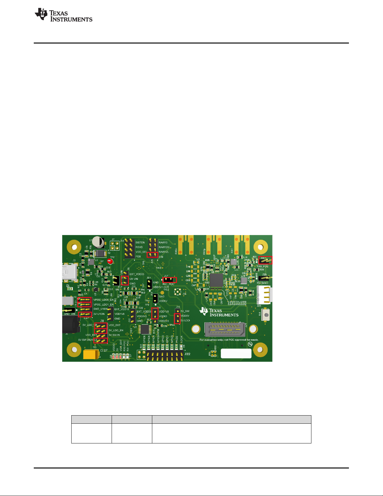
2. Configure jumpers J8, J10, J11, J15, J16, J23, J27, set device’s operating modes. The default
configuration can be see in
3. Configure Power Over Coax power supplies for RX0 and RX1 with J18 and J17 respectively.
4. Connect the DS90UB954-Q1EVM to DS90UB953-Q1EVM to RX0 and/or DS90UB933-Q1EVM to RX1
using coax cable
5. Interface MIPI CSI-2 output signals (J24) to test equipment or host processor (optional, not required to
check status of FPD-Link III connection between serializer and deserializer)
6. Provide power to board. TI recommends using current limited bench supply to provide power to J1
(barrel jack) or J3.
3 DS90UB954-Q1EVM Board Configuration -Evaluation Board Connections
3.1 Default Configuration
Default jumper placement shown in red. This configuration sets the device into the following mode
• Device is set for FPD-Link III inputs from coax in CSI mode (for DS90UB953-Q1)
• VDDIO is set to 1.8V
• VDD5V is powered by the 5V LDO
• The 3.3V + 1.1V LDO (U10) is powered by VDD5V
• The 9V LDO for POC for RX0 and RX1 are enabled
Quick Start Guide
•
3.2 Power Supply
Reference Signal Description
J1/J3 +12V
SNLU223–August 2017
Submit Documentation Feedback
Figure 4. DS90UB954-Q1EVM with Jumpers Highlighted
Table 1. Power Supply
Main Power
Single +12VDC (nominal) power connector that supplies power to the
entire board.
DS90UB954-Q1EVM Quick Start
Copyright © 2017, Texas Instruments Incorporated
5
Page 6
DS90UB954-Q1EVM Board Configuration -Evaluation Board Connections
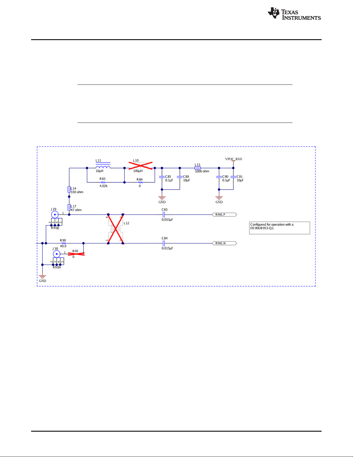
3.3 Power Over Coax Interface
The DS90UB954-Q1EVM offers two power over coax interfaces (POC) to connect cameras through a
coaxial cable with FAKRA connectors. Power is delivered on the same conductor that is used to transmit
video and control channel data between the host and the camera. By default, 5V power supply is applied
over the coax cable. Refer to Table 2 for other POC configurations.
NOTE: For port RX0, the POC network is configured for a DS90UB953-Q1, and for RX1 the POC
network is configured for a DS90UB933-Q1. Only use a serializer EVM with the correct POC
network. To use POC with two DS90UB953-Q1 or DS90UB933-Q1 EVM's, one of the POC
networks must be reworked. You may also open the POC circuit and power the serializer
EVM directly from another supply.
For power over coax (POC) on the EVM, the circuit uses a filter network as shown in Figure 6. The POC
network frequency response corresponds to the bandwidth compatible with DS90UB953-Q1 chipsets.
www.ti.com
Figure 5. Power Over Coax Network For Use With DS90UB953
6
DS90UB954-Q1EVM Quick Start
Copyright © 2017, Texas Instruments Incorporated
Submit Documentation Feedback
SNLU223–August 2017
Page 7

www.ti.com
DS90UB954-Q1EVM Board Configuration -Evaluation Board Connections
Figure 6. Power Over Coax Network For Use With DS90UB933
WARNING
Verify that the power over coax voltage is properly set before
plugging into RX0 or RX1. Power supply is not fused. Over-voltage
will cause damage to boards directly connected due to incorrect
input power supplies. DS90UB913A-Q1EVM is designed for a
maximum of 5V POC. To use DS90UB913A-Q1EVM with
DS90UB954-Q1EVM, open J17 or J18 to disable POC, and either
power the DS90UB913A-Q1EVM separately or by applying 5V to the
J17 or J18 pin on DS90UB954-Q1EVM.
Table 2. Power Over Coax Power Supply Feed Configuration
Reference Signal Description
This sets the voltage for Power over Coax on RX0
J18 VPOC_RX0
J17 VPOC_RX1
Jumper installed: +9V power supply from VPOC_LDO0_9V
Jumper Open: No POC connected. Apply power to pin1 or leave
open and power serializer separately.
This sets the voltage for Power over Coax on RX1
Jumper installed: +9V power supply from VPOC_LDO1_9V
Jumper Open: No POC connected. Apply power to pin1 or leave
open and power serializer separately.
SNLU223–August 2017
Submit Documentation Feedback
Copyright © 2017, Texas Instruments Incorporated
DS90UB954-Q1EVM Quick Start
7
Page 8

DS90UB954-Q1EVM Board Configuration -Evaluation Board Connections
3.4 MIPI CSI-2 Output Signals
There are two options provided for passing out the deserialized data on the DS90UB954-Q1EVM. The first
is a Samtec QSH-type connector, J24, on the top of the board that can be mated with a matching QTH
type connector. The mating connector part number for the J24 connector is QTH-020-01-H-D-DP-A. On
the bottom of the board is a Samtec QTH-type connector, J26, meant for mating with a TDAx evaluation
kit. The signals to the connectors are the same, including access to I2C and other signals including PDB
and GPIO. Only one connector should be used at a time. If the J6 connector on the bottom is to be used,
populate the zero ohm resistors on the bottom of the board which extend the traces to the J26 connector.
There are third party solutions like the HDR-128291-XX breakout board from Samtec which can be used.
The HDR- 128291-XX is a breakout board with a mating connector to J24 or J26, providing access to
each pin through standard SMA male connectors. More info on this breakout board can be obtained from
Samtec website. Another third party option is the ZX100 by Zebax Technologies. More information on this
board can be obtained from Zebax website.
Table 3. MIPI CSI-2 Output Signals - J5 and J6 Pinout
Pin # Signal Name Pin # Signal Name
1 NC 2
3 NC 4
5 CSI_CLK0_P 6 NC
7 CSI_CLK0_N 8 NC
9 CSI_D0_P 10
11 CSI_D0_N 12 GND
13 CSI_D1_P 14
15 CSI_D1_N 16 GND
17 CSI_D2_P 18
19 CSI_D2_N 20
21 CSI_D3_P 22
23 CSI_D3_N 24 GND
25 CSI_CLK1_P 26 NC
27 CS_CLK1_N 28 NC
29 NC 30 VDD_3V3
31 NC 32 VDD_3V3
33 NC 34 VDD_3V3
35 NC 36 VDD_3V3
37 NC 38 VDD_1V8
39 NC 40 VDD_1V8
www.ti.com
EXP_SCL
(I2C_SCL or I2C_SCL2)
EXP_SDA
(I2C_SDA or I2C_SDA2)
EXP_REF_CLK
(REFCLK)
RESETn
(PDB)
SPI_MOSI
(GPIO0 or GPIO3)
SPI_SCLK
(GPIO1 or GPIO4)
SPI_CSn
(GPIO2 or GPIO5)
NOTE: Populate R60-R69, R71,R72 (0Ω resistors) only when using the J26 connector on the bottom
of the board. Do not use J24 and J26 connectors at the same time.
8
DS90UB954-Q1EVM Quick Start
Copyright © 2017, Texas Instruments Incorporated
Submit Documentation Feedback
SNLU223–August 2017
Page 9
www.ti.com
3.5 FPD-Link III Signals
Reference Signal Description
RX0p RIN0+ FAKRA connector for DS90UB953-Q1 serializer
RX0n RIN0- FAKRA connector footprint for use with STP applications.
RX1 RIN1+ FAKRA connector for DS90UB933-Q1 serializer
3.6 I2C Interface
In addition to the on-board USB2ANY controller accessible via the mini-USB port, a standalone external
I2C host can connect via J25 for programming purposes. Examples of external I2C host controllers are
Texas Instruments USB2ANY and Total Phase Aardvark I2C/SPI host adapter (Total Phase Part#:
TP240141).
When the I2C interface is accessed through connector J25, I2C signal levels can be configured through
J16 to be at 1.8V or 3.3V. Optional access to I2C signals are also available via CSI-2 connectors J24 (top)
and J26 (bottom).
Reference Signal Description
J23 IDX Select
DS90UB954-Q1EVM Board Configuration -Evaluation Board Connections
Table 4. FPD-Link III Signals
Table 5. IDx I2C Device Address Select - J23
Selects I2C Device Address
Open: 0x30 (7'b) or 0x60 (8'b)
Short: 0x3D (7'b) or 0x7A (8'b) (Default)
Table 6. I2C Interface Header - J25
Reference Signal Description
J25.1 VDDIO I2C bus voltage (tied to VDDIO)
J25.2 I2C_SCL I2C Clock Interface for I2C bus
J25.3 I2C_SDA I2C Data Interface for I2C bus
J25.4 GND Ground
SNLU223–August 2017
Submit Documentation Feedback
Copyright © 2017, Texas Instruments Incorporated
DS90UB954-Q1EVM Quick Start
9
Page 10
DS90UB954-Q1EVM Board Configuration -Evaluation Board Connections
3.7 Control Interface
Table 7. VDDIO Interface Header - J16
Reference Signal Description
Selects VDDIO bus voltage
J16 VDDIO
Table 8. GPIO Interface Header - J22
Reference Signal Description
J22.1 GPIO0 General Purpose Input/Output 0
J22.3 GPIO1 General Purpose Input/Output 1
J22.5 GPIO2 General Purpose Input/Output 2
J22.7 GPIO3/INTB
J22.9 GPIO4 General Purpose Input/Output 4
J22.11 GPIO5 General Purpose Input/Output 5
J22.13 GPIO6 General Purpose Input/Output 6
J22.15 EN 25MHz Enable/Disable 25MHz Oscillator
Short pins 1-2: 3.3V IO (Default)
Short pins 2-3: 1.8V IO
General Purpose Input/Output 3 / Interrupt (Active Low).
Pulled up to VDDIO by 4.7kΩ
www.ti.com
Table 9. CMLOUTP Output Signals
Reference Signal Description
TP16 CMLOUTP Test Pad for Channel Monitor Loop-through Driver
TP17 CMLOUTN Test Pad for Channel Monitor Loop-through Driver
Table 10. FPD-Link III Mode Control- J15
Reference Mode Description
J15.1 1 CSI Mode (DS90UB953-Q1 compatible)
J15.2 2 RAW12 / LF (DS90UB933 compatible)
J15.3 3 RAW12 / HF (DS90UB933 compatible)
J15.4 4 RAW10 (DS90UB933 compatible)
(1)
Only set one ON.
(2)
This function is only available with 2-MP ADAS chipsets.
(1)
(2)
Table 11. Device Mode Control - J11
Reference Signal Input = L Input = H Description
J11.1 BISTEN
J11.2 RSVD Tied to GND (Default) N/A Reserved
J11.3 VDD_SEL
J11.4 PDB Device is powered down Device is enabled (Default) Power-down Mode
For Normal operation
(Default)
Internal 1.1V regulator from
1.8V supply (Default)
Test Mode enable Test Mode
1.1V is supplied to VDD1V1
pins
VDD 1.1V Source Select
10
DS90UB954-Q1EVM Quick Start
Submit Documentation Feedback
SNLU223–August 2017
Copyright © 2017, Texas Instruments Incorporated
Page 11

www.ti.com
Table 12. LEDs
Reference LED Color LED Name Description
D3 Red VDDIO Illuminates on VDDIO Power
D4 Red VDD5V Illuminates on +5V
D5 Red VDD_EXT Illuminates if 12V Power is applied to DC-IN J24
D6 Orange VPOC_RX1 Illuminates if VPOC_RX1 is ON
D7 Orange VPOC_RX0 Illuminates if VPOC_RX0 is ON
D8 Orange PASS Illuminates if PASS pin is HIGH
D9 Green LOCK Illuminates if LOCK pin is HIGH
D10 Green GPIO6 Illuminates if GPIO6 is HIGH
D11 Green GPIO5 Illuminates if GPIO5 is HIGH
D12 Green GPIO4 Illuminates if GPIO48 is HIGH
D13 Green GPIO3/INTB Illuminates if GPIO3 is HIGH, or GPIO3 disabled (pulled-up)
D14 Green GPIO2 Illuminates if GPIO2 is HIGH
D15 Green GPIO1 Illuminates if GPIO1 is HIGH
D16 Green GPIO0 Illuminates if GPIO0 is HIGH
4 Enable and Reset
The DS90UB954-Q1 is enabled and reset by controlling the PDB input level. PDB has an internal pull
down, and should remain low until all supplies are stable. There are three device enable and reset/power-
down options for the EVM.
• RC timing option: The RC delay created with C123 and R131 connected to the PDB pin is the default
option for delaying PDB on the EVM. This is used for simplicity of debugging and using the device. TI
recommends using a GPIO signal from a host process or to drive PDB after all rails have settled in
customer designs.
• External control option: A momentary push-button switch, SW1, is available for manually driving the
PDB signal low while the button is held.
• Software control option: The PDB pin is also made available in the J24 and J26 CSI-2 output
connectors, allowing a host processor to control the PDB pin.
Enable and Reset
SNLU223–August 2017
Submit Documentation Feedback
Copyright © 2017, Texas Instruments Incorporated
DS90UB954-Q1EVM Quick Start
11
Page 12

Typical Connection and Test Equipment
5 Typical Connection and Test Equipment
The following is a list of typical test equipment that may be used to monitor the MIPI CSI-2 signals from
the DS90UB954-Q1:
1. Logic Analyzer
2. Any SCOPE with a bandwidth of at least 4 GHz for observing differential signals.
3. UNH-IOL MIPI D-PHY Reference Termination Board (RTB)
4. UNH-IOL MIPI D-PHY/CSI/DSI Probing Board
5. UNH-IOL CSIGUI Tool
6 Termination Device
A termination device is required to properly monitor and measure the transmission of the MIPI DPHY
signals. The termination device should support the change of signals as it switches between LP and HS
modes. This can be provided by either a CSI-2 receiver or a dedicated dynamic termination board. The
recommended termination board is the UNH-IOL MIPI D-PHY Reference Termination Board (RTB).
7 Typical Test Setup
Figure 7 illustrate the typical test setups used to measure and evaluate DS90UB954-Q1.
Figure 7 shows a typical test set up using a logic analyzer or oscilloscope.
www.ti.com
12
DS90UB954-Q1EVM Quick Start
Figure 7. Typical Test Setup for Evaluation
Copyright © 2017, Texas Instruments Incorporated
Submit Documentation Feedback
SNLU223–August 2017
Page 13

www.ti.com
8 Equipment References
NOTE: Please note that the following references are supplied only as a courtesy to our valued
customers. It is not intended to be an endorsement of any particular equipment or supplier.
Logic Analyzer:
Keysight Technologies
www.keysight.com
MIPI Test Fixtures:
University of New Hampshire InterOperability Laboratory (UNH-IOL)
www.iol.unh.edu/services/testing/mipi/fixtures.php
Aardvark I2C/SPI Host Adapter Part Number: TP240141
www.totalphase.com/products/aardvark_i2cspi
9 Cable References
FAKRA coaxial cable:
www.leoni-automotive-cables.com
Equipment References
Rosenberger FAKRA connector:
http://www.rosenberger.com/en/products/automotive/fakra.php
SNLU223–August 2017
Submit Documentation Feedback
Copyright © 2017, Texas Instruments Incorporated
DS90UB954-Q1EVM Quick Start
13
Page 14

Software for DS90UB954Q1-EVM Evaluation - Analog LaunchPAD (ALP) Software Setup
www.ti.com
10 Software for DS90UB954Q1-EVM Evaluation - Analog LaunchPAD (ALP) Software Setup
10.1 System Requirements
Operating System: Windows 7 64-bit
USB: USB2ANY (on-board, accessible
via mini USB connector)
USB2ANY Firmware Version: 2.5.2.0
USB: Aardvark I2C/SPI host adapter
p/n TP240141
10.2 Download Contents
Latest TI Analog LaunchPAD can be downloaded from: http://www.ti.com/tool/alp.
Download and extract the zip file to a temporary location that can be deleted later.
The following installation instructions are for a PC running Windows 7 64-bit Operating System.
10.3 Installation of the ALP Software
Execute the ALP Setup Wizard program called “ALPF_setup_v_x_x_x.exe” that was extracted to a
temporary location on the local drive of your PC.
There are 7 steps to the installation once the setup wizard is started:
1. Select the "Next" button.
2. Select “I accept the agreement” and then select the “Next” button.
3. Select the location to install the ALP software and then select the “Next” button.
4. Select the location for the start menu shortcut and then select the “Next” button.
5. There will then be a screen that allows the creation of a desktop icon. After selecting the desired
choices select the “Next” button.
6. Select the “Install” button, and the software will then be installed to the selected location.
7. Uncheck “Launch Analog LaunchPAD” and select the “Finish” button. The ALP software will start if
“Launch Analog LaunchPAD” is checked, but it will not be useful until the USB driver is installed and
board is attached.
Power the DS90UB954-Q1 EVM board with a 12 VDC power supply.
14
DS90UB954-Q1EVM Quick Start
Copyright © 2017, Texas Instruments Incorporated
Submit Documentation Feedback
SNLU223–August 2017
Page 15
www.ti.com
10.4 Startup - First Launch
Make sure all the software has been installed and the hardware is powered on and connected to the PC.
Execute “Analog LaunchPAD” shortcut from the start menu. The default start menu location is under All
Programs > Texas Instruments > Analog LaunchPAD vx.x.x > Analog LaunchPAD to start MainGUI.exe.
Software for DS90UB954Q1-EVM Evaluation - Analog LaunchPAD (ALP) Software Setup
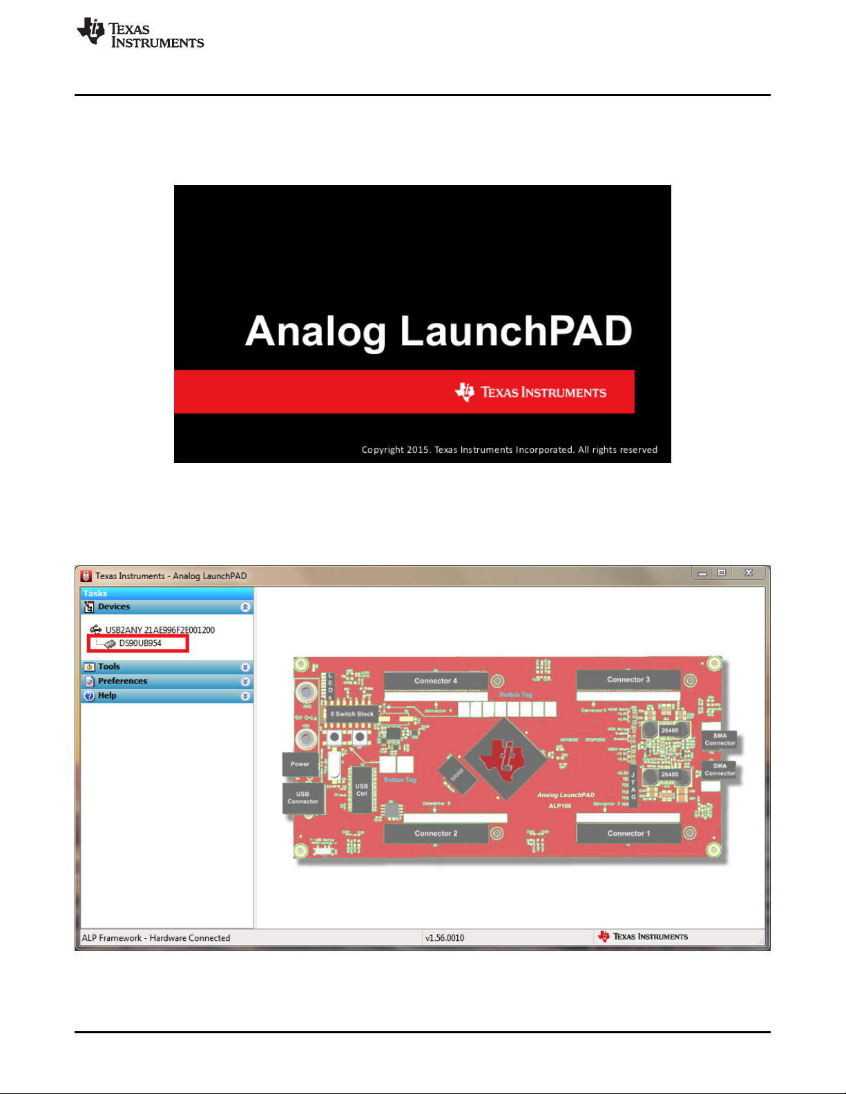
Figure 8. Launching ALP Splash Screen
Upon first launch of the Analog LaunchPAD utility, the default device will be DS90UB925. The active
device can be seen as highlighted in ,here showing the DS90UB954 as active. If the active device is
already set to DS90UB954 you may skip to .
SNLU223–August 2017
Submit Documentation Feedback
Figure 9. Initial ALP Screen
Copyright © 2017, Texas Instruments Incorporated
DS90UB954-Q1EVM Quick Start
15
Page 16
Software for DS90UB954Q1-EVM Evaluation - Analog LaunchPAD (ALP) Software Setup
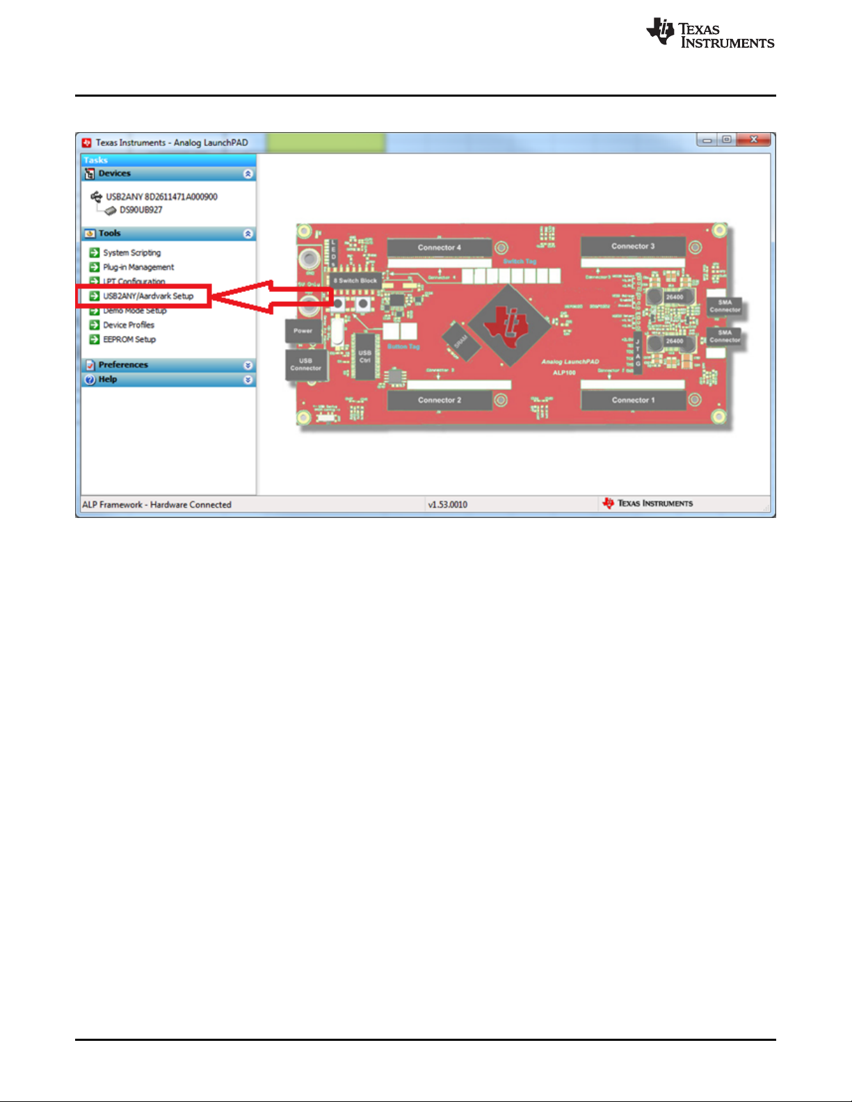
Follow the steps beginning with to change the ALP profile to DS90UB954.
www.ti.com
Figure 10. Select USB2ANY/Aardvark Setup to Change Profile
16
DS90UB954-Q1EVM Quick Start
Copyright © 2017, Texas Instruments Incorporated
Submit Documentation Feedback
SNLU223–August 2017
Page 17
www.ti.com
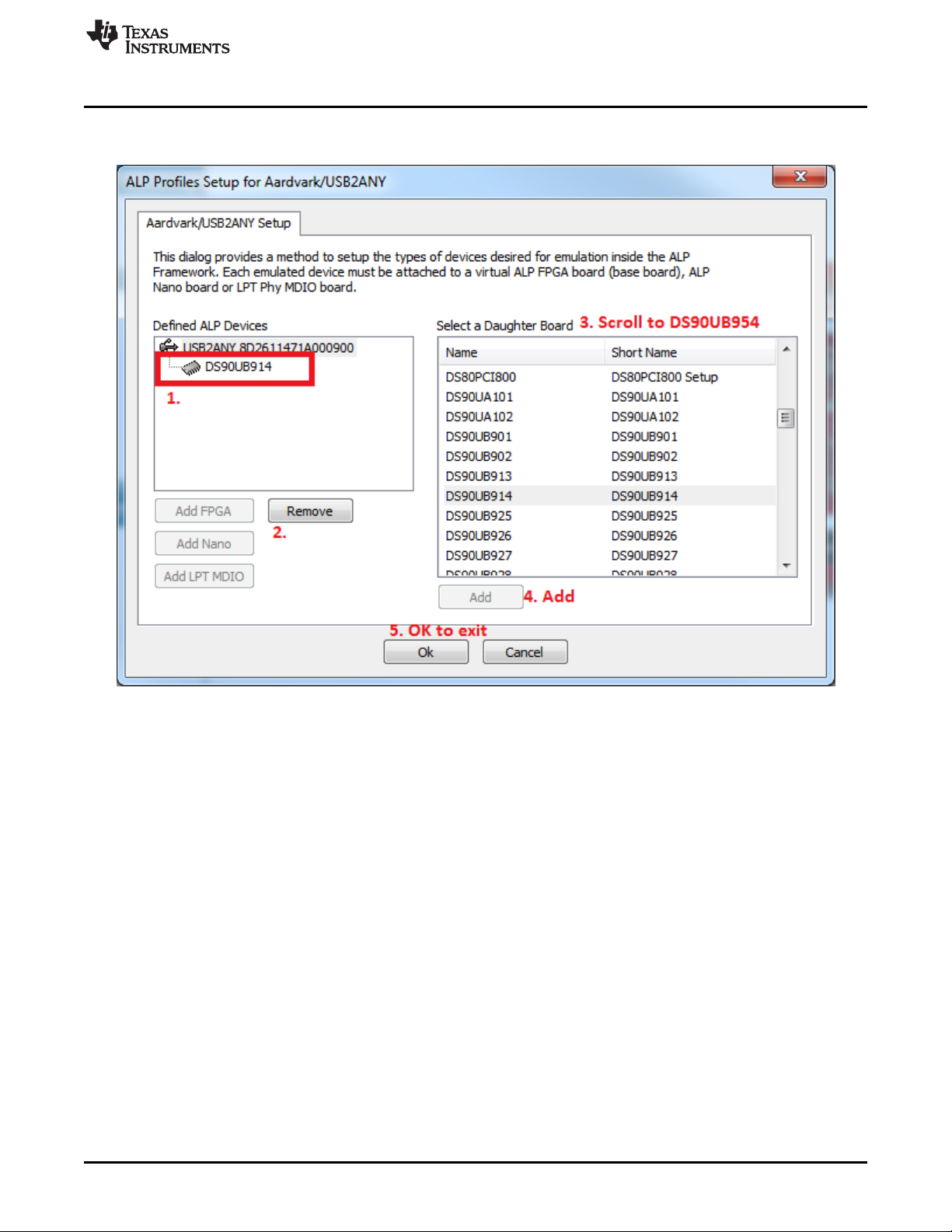
Select the active profile and click "Remove". Scroll down the list of available profiles to DS90UB954, click
to highlight it, click "Add", and click "Ok".
Software for DS90UB954Q1-EVM Evaluation - Analog LaunchPAD (ALP) Software Setup
Figure 11. ALP Profiles Dialog
SNLU223–August 2017
Submit Documentation Feedback
Copyright © 2017, Texas Instruments Incorporated
DS90UB954-Q1EVM Quick Start
17
Page 18

Software for DS90UB954Q1-EVM Evaluation - Analog LaunchPAD (ALP) Software Setup
www.ti.com
Figure 12. ALP Profiles Dialog (continued)
18
DS90UB954-Q1EVM Quick Start
Copyright © 2017, Texas Instruments Incorporated
Submit Documentation Feedback
SNLU223–August 2017
Page 19

www.ti.com
11 Using ALP and DS90UB954 Profile
11.1 Information Tab
Under the Devices tab click on “DS90UB954” to select the device and open up the device profile and its
associated tabs. After selecting the DS90UB954, the following screen shown in should appear. Figure 13
shows the Information tab. The information tab shown assumes active and locked connection to a
DS90UB953 on RX0, and an open port on RX1.
Using ALP and DS90UB954 Profile
Figure 13. ALP Information Tab
SNLU223–August 2017
Submit Documentation Feedback
Copyright © 2017, Texas Instruments Incorporated
DS90UB954-Q1EVM Quick Start
19
Page 20

Using ALP and DS90UB954 Profile
11.2 Registers Tab
The Register tab is shown in Figure 14. Note that the value of the currently selected register is populated
in the "Value: " box at the top. Figure 14 shows the register I2C_DEVICE_ID is reading a hexidecimal
value of 0x60.
www.ti.com
Figure 14. ALP Registers Tab
20
DS90UB954-Q1EVM Quick Start
Copyright © 2017, Texas Instruments Incorporated
Submit Documentation Feedback
SNLU223–August 2017
Page 21

www.ti.com
11.3 Registers Tab - Address 0x00 Expanded
By double clicking on the Address bar
or a single click on . Address 0x00 expanded reveals contents by bits. Any register address displayed
can be expanded.
Using ALP and DS90UB954 Profile
Figure 15. ALP Device ID Expanded
Any RW Type register can be written into by writing the hex value into the “Value:” box, or
putting the pointer into the individual register bit(s) box by a left mouse click to put a check mark
(indicating a “1”) or unchecking to remove the check mark (indicating a “0”). Click the “Apply” button to
write to the register, and “refresh” to see the new value of the selected (highlighted) register.
The box toggles on every mouse click.
SNLU223–August 2017
Submit Documentation Feedback
Copyright © 2017, Texas Instruments Incorporated
DS90UB954-Q1EVM Quick Start
21
Page 22

Using ALP and DS90UB954 Profile
11.4 Scripting Tab
Figure 16 shows the Scripting tab.
www.ti.com
The script window provides a full Python scripting environment which can be for running scripts and
interacting with the device in an interactive or automated fashion.
Directly interacting with devices either through register
modifications or calling device support library functions can effect
the performance and/or functionality of the user interface and may
even crash the ALP Framework application.
11.5 Sample ALP Python Script
The following are sample python scripts that should be run before attempting to transmit video data from a
serializer. The code can be saved as a python script and run from the ALP scripting tab by click "Run" and
opening the saved script. The script will execute as soon as the dialog box closes.
Figure 16. ALP Scripting Tab
WARNING
22
DS90UB954-Q1EVM Quick Start
Copyright © 2017, Texas Instruments Incorporated
Submit Documentation Feedback
SNLU223–August 2017
Page 23

www.ti.com
12 Troubleshooting ALP Software
12.1 ALP Does Not Detect The EVM
If the following window opens after starting the ALP software, double check the hardware setup.
Figure 17. ALP No Devices Error
It may also be that the USB2ANY driver is not installed. Check the device manager. There should be a
“HID-compliant device” under the “Human Interface Devices” as shown in Figure 18.
Troubleshooting ALP Software
The software should start with only “DS90UB954” in the “Devices” pull down menu. If there are more
devices then the software is most likely in demo mode. When the ALP is operating in demo mode there is
a “(Demo Mode)” indication in the lower left of the application status bar as shown in Figure 19.
SNLU223–August 2017
Submit Documentation Feedback
Figure 18. Windows 7, ALP USB2ANY Driver
Copyright © 2017, Texas Instruments Incorporated
DS90UB954-Q1EVM Quick Start
23
Page 24

Troubleshooting ALP Software
Disable the demo mode by selecting the “Preferences” pull down menu and un-checking “Enable Demo
Mode”.
www.ti.com
Figure 19. ALP in Demo Mode
After demo mode is disabled, the ALP software will poll the ALP hardware. The ALP software will update
and have only “DS90UB954” under the “Devices” pull down menu.
12.2 USB2ANY Firmware Issues
If upon plugging in the board to the PC, the user is presented with a message stating USB2ANY firmware
is out of date or is 0.0.0.0, similar to Figure 21, try unplugging the USB cable and plugging it in again
(holding S1 while plugging in the USB cable puts the USB2ANY into firmware update mode). If that does
not solve the problem you will have to re-flash the on-board USB2ANY firmware. To re-flash the
USB2ANY, download USB2ANY Explorer USB2ANY Explorer Installer v2.7.0.0 and install the application.
Launch the USB2ANY Firmware Loader available at "C:\Program Files (x86)\TI USB2ANY
SDK\bin\USB2ANY Firmware Loader.exe" and follow the instructions to flash the latest version of
USB2ANY firmware. The firmware loading screen is shown in Figure 22.
Figure 20. ALP Preferences Menu
24
DS90UB954-Q1EVM Quick Start
Copyright © 2017, Texas Instruments Incorporated
Submit Documentation Feedback
SNLU223–August 2017
Page 25

www.ti.com
Troubleshooting ALP Software
Figure 21. USB2ANY Firmware Update Notice
SNLU223–August 2017
Submit Documentation Feedback
Figure 22. USB2ANY Firmware Update Procedure
DS90UB954-Q1EVM Quick Start
Copyright © 2017, Texas Instruments Incorporated
25
Page 26

DS90UB954-Q1EVM PCB Schematics, Layout and Bill of Materials - DS90UB954-Q1EVM Schematic
13 DS90UB954-Q1EVM PCB Schematics, Layout and Bill of Materials - DS90UB954-Q1EVM Schematic
www.ti.com
26
DS90UB954-Q1EVM Quick Start
Figure 23. DS90UB954-Q1EVM Block Diagram
SNLU223–August 2017
Submit Documentation Feedback
Copyright © 2017, Texas Instruments Incorporated
Page 27

www.ti.com
DS90UB954-Q1EVM PCB Schematics, Layout and Bill of Materials - DS90UB954-Q1EVM Schematic
SNLU223–August 2017
Submit Documentation Feedback
Figure 24. DS90UB954-Q1EVM Maine Circuit - Page 1
Copyright © 2017, Texas Instruments Incorporated
DS90UB954-Q1EVM Quick Start
27
Page 28

DS90UB954-Q1EVM PCB Schematics, Layout and Bill of Materials - DS90UB954-Q1EVM Schematic
www.ti.com
28
DS90UB954-Q1EVM Quick Start
Figure 25. DS90UB954-Q1EVM CSI-2 Connectors - Page 2
SNLU223–August 2017
Submit Documentation Feedback
Copyright © 2017, Texas Instruments Incorporated
Page 29

www.ti.com
DS90UB954-Q1EVM PCB Schematics, Layout and Bill of Materials - DS90UB954-Q1EVM Schematic
SNLU223–August 2017
Submit Documentation Feedback
Figure 26. DS90UB954-Q1EVM PoC Circuits - Page 3
Copyright © 2017, Texas Instruments Incorporated
DS90UB954-Q1EVM Quick Start
29
Page 30

DS90UB954-Q1EVM PCB Schematics, Layout and Bill of Materials - DS90UB954-Q1EVM Schematic
www.ti.com
30
DS90UB954-Q1EVM Quick Start
Figure 27. DS90UB954-Q1EVM Power Distribution Circuits - Page 4
SNLU223–August 2017
Submit Documentation Feedback
Copyright © 2017, Texas Instruments Incorporated
Page 31

www.ti.com
DS90UB954-Q1EVM PCB Schematics, Layout and Bill of Materials - DS90UB954-Q1EVM Schematic
SNLU223–August 2017
Submit Documentation Feedback
Figure 28. DS90UB954-Q1EVM LED Circuits - Page 5
Copyright © 2017, Texas Instruments Incorporated
DS90UB954-Q1EVM Quick Start
31
Page 32

DS90UB954-Q1EVM PCB Schematics, Layout and Bill of Materials - DS90UB954-Q1EVM Schematic
www.ti.com
32
DS90UB954-Q1EVM Quick Start
Figure 29. DS90UB954-Q1EVM USB2ANY Circuits - Page 6
SNLU223–August 2017
Submit Documentation Feedback
Copyright © 2017, Texas Instruments Incorporated
Page 33

www.ti.com
DS90UB954-Q1EVM PCB Schematics, Layout and Bill of Materials - DS90UB954-Q1EVM Schematic
SNLU223–August 2017
Submit Documentation Feedback
Figure 30. DS90UB954-Q1EVM Miscellaneous Hardware
Copyright © 2017, Texas Instruments Incorporated
DS90UB954-Q1EVM Quick Start
33
Page 34

PDS90UB954-Q1 EVM PCB Layout
14 PDS90UB954-Q1 EVM PCB Layout
www.ti.com
34
DS90UB954-Q1EVM Quick Start
Figure 31. Top View Composite
SNLU223–August 2017
Submit Documentation Feedback
Copyright © 2017, Texas Instruments Incorporated
Page 35

www.ti.com
PDS90UB954-Q1 EVM PCB Layout
SNLU223–August 2017
Submit Documentation Feedback
Figure 32. Layer 1: Top Signal Layer
Copyright © 2017, Texas Instruments Incorporated
DS90UB954-Q1EVM Quick Start
35
Page 36

PDS90UB954-Q1 EVM PCB Layout
www.ti.com
36
DS90UB954-Q1EVM Quick Start
Figure 33. Layer 2: GND Plane 1
SNLU223–August 2017
Submit Documentation Feedback
Copyright © 2017, Texas Instruments Incorporated
Page 37

www.ti.com
PDS90UB954-Q1 EVM PCB Layout
SNLU223–August 2017
Submit Documentation Feedback
Figure 34. Layer 3: Mid Signal Layer 1
Copyright © 2017, Texas Instruments Incorporated
DS90UB954-Q1EVM Quick Start
37
Page 38

PDS90UB954-Q1 EVM PCB Layout
www.ti.com
38
DS90UB954-Q1EVM Quick Start
Figure 35. Layer 4: GND Plane 2
SNLU223–August 2017
Submit Documentation Feedback
Copyright © 2017, Texas Instruments Incorporated
Page 39

www.ti.com
PDS90UB954-Q1 EVM PCB Layout
SNLU223–August 2017
Submit Documentation Feedback
Figure 36. Layer 5: GND Plane 3
Copyright © 2017, Texas Instruments Incorporated
DS90UB954-Q1EVM Quick Start
39
Page 40

PDS90UB954-Q1 EVM PCB Layout
www.ti.com
40
DS90UB954-Q1EVM Quick Start
Figure 37. Layer 6: Mid Signal Layer 2
SNLU223–August 2017
Submit Documentation Feedback
Copyright © 2017, Texas Instruments Incorporated
Page 41

www.ti.com
PDS90UB954-Q1 EVM PCB Layout
SNLU223–August 2017
Submit Documentation Feedback
Figure 38. Layer 7: GND Plane 4
Copyright © 2017, Texas Instruments Incorporated
DS90UB954-Q1EVM Quick Start
41
Page 42

PDS90UB954-Q1 EVM PCB Layout
www.ti.com
42
DS90UB954-Q1EVM Quick Start
Figure 39. Layer 8: Bottom Signal Layer
SNLU223–August 2017
Submit Documentation Feedback
Copyright © 2017, Texas Instruments Incorporated
Page 43

www.ti.com
PDS90UB954-Q1 EVM PCB Layout
SNLU223–August 2017
Submit Documentation Feedback
Figure 40. Bottom View Composite
Copyright © 2017, Texas Instruments Incorporated
DS90UB954-Q1EVM Quick Start
43
Page 44

DS90UB954Q1-EVM Bill of Materials
15 DS90UB954Q1-EVM Bill of Materials
Table 13. DS90UB954-Q1EVM BOM
www.ti.com
ITEM QTY DESIGNATOR VALUE PART NUMBER MANUFACT
1 1 !PCB1 HSDC007 Any Printed Circuit Board
2 2 C1, C8 220pF 06035A221FAT2A AVX CAP, CERM, 220 pF, 50 V, +/- 1%,
3 1 C2 0.01uF C1608X7R1H103K080AA TDK CAP, CERM, 0.01 µF, 50 V, +/-
4 5 C3, C13, C14,
C75, C111
5 2 C4, C12 0.1uF GRM155R71C104KA88D MuRata CAP, CERM, 0.1 µF, 16 V, +/-
6 1 C5 1uF C0805C105K3RACTU Kemet CAP, CERM, 1 µF, 25 V, +/- 10%,
7 1 C6 2.2uF 0805YD225KAT2A AVX CAP, CERM, 2.2 µF, 16 V, +/-
8 1 C7 22uF EEE-1AA220WR Panasonic -
9 2 C9, C10 30pF GRM1885C2A300JA01D MuRata CAP, CERM, 30 pF, 100 V, +/- 5%,
10 1 C11 2200pF C0603X222K5RACTU Kemet CAP, CERM, 2200 pF, 50 V, +/-
11 4 C15, C19, C105,
C109
12 5 C16, C20, C110,
C114, C123
13 12 C17, C18, C21,
C22, C51, C113,
C116, C117,
C121, C122,
C125, C128
14 1 C23 10pF GRM1555C1H100JA01D MuRata CAP, CERM, 10pF, 50V, +/-5%,
15 1 C24 3300pF GRM155R71H332KA01D MuRata CAP, CERM, 3300pF, 50V, +/-
16 2 C25, C124 1uF GCM188R71C105KA64D MuRata CAP, CERM, 1 µF, 16 V, +/- 10%,
17 9 C26, C28, C30,
C31, C101, C102,
C104, C119,
C120
18 1 C27 10uF GRM188R61E106MA73D MuRata CAP, CERM, 10 µF, 25 V, +/-
19 14 C29, C34, C40,
C41, C48, C49,
C53, C54, C62,
C67, C81, C86,
C87, C93
20 2 C32, C35 22uF GRT31CR61E226KE01L MuRata CAP, CERM, 22 µF, 25 V, +/-
21 8 C33, C42, C47,
C63, C66, C71,
C78, C79
22 4 C36, C43, C61,
C72
0.1uF 0603YC104JAT2A AVX CAP, CERM, 0.1 µF, 16 V, +/- 5%,
4.7uF GRM21BR71C475KA73L MuRata CAP, CERM, 4.7uF, 16V, +/-10%,
10uF GRM21BR71A106KE51L MuRata CAP, CERM, 10uF, 10V, +/-10%,
0.1uF GRM155R71C104KA88D MuRata CAP, CERM, 0.1uF, 16V, +/-10%,
1uF GRM185R61C105KE44D MuRata CAP, CERM, 1 µF, 16 V, +/- 10%,
22uF GRT31CR61E226KE01L MuRata CAP, CERM, 22 µF, 25 V,+/- 10%,
0.1uF CGA2B3X7R1H104K050BB TDK CAP, CERM, 0.1 µF, 50 V, +/-
4.7uF C0805C475K3PACTU Kemet CAP, CERM, 4.7 µF, 25 V, +/-
URER
ECG
DESCRIPTION
C0G/NP0, 0603
10%, X7R, 0603
X7R, 0603
10%, X7R, 0402
X7R, 0805
10%, X5R, 0805
CAP ALUM 22UF 10V 20% SMD
C0G/NP0, 0603
10%, X7R, 0603
X7R, 0805
X7R, 0805
X7R, 0402
C0G/NP0, 0402
10%, X7R, 0402
X7R, AEC-Q200 Grade 1, 0603
X5R, 0603
20%, X5R, 0603
X5R, AEC-Q200 Grade 3, 1206
10%, X5R, AEC-Q200 Grade 3,
1206
10%, X7R, AEC-Q200 Grade 1,
0402
10%, X5R, 0805
44
DS90UB954-Q1EVM Quick Start
Submit Documentation Feedback
SNLU223–August 2017
Copyright © 2017, Texas Instruments Incorporated
Page 45

www.ti.com
ITEM QTY DESIGNATOR VALUE PART NUMBER MANUFACT
23 9 C37, C44, C45,
24 3 C38, C39, C83 0.033uF CGA2B3X7R1H333K050BB TDK CAP, CERM, 0.033 µF, 50 V, +/-
25 8 C46, C59, C73,
26 2 C50, C106 0.1uF C1005X5R1H104K050BB TDK CAP, CERM, 0.1 µF, 50 V, +/-
27 4 C52, C56, C130,
28 2 C55, C58 12pF GRM1555C1E120JA01D MuRata CAP, CERM, 12pF, 25V, +/-5%,
29 3 C57, C88, C92 10uF CL21A106KAFN3NE Samsung CAP, CERM, 10 µF, 25 V, +/-
30 4 C69, C94, C99,
31 5 C70, C85, C90,
32 1 C74 0.01uF 06031C103KAT2A AVX CAP, CERM, 0.01 µF, 100 V, +/-
33 1 C76 0.047uF C1005X7R1H473K050BB TDK CAP, CERM, 0.047 µF, 50 V, +/-
34 1 C84 0.015uF CGA2B3X7R1H153K050BB TDK CAP, CERM, 0.015 µF, 50 V, +/-
35 4 C89, C91, C95,
36 1 C107 47uF GRM32ER61C476ME15L MuRata CAP, CERM, 47uF, 16V, +/-20%,
37 1 C108 100uF T495D107M016ATE100 Kemet CAP, TA, 100uF, 16V, +/-20%, 0.1
38 1 C115 0.01uF 06031C103JAT2A AVX CAP, CERM, 0.01uF, 100V, +/-5%,
39 1 C126 0.47uF GRM188R71A474KA61D MuRata CAP, CERM, 0.47 µF, 10 V, +/-
40 1 C129 2.2uF 293D225X9025A2TE3 Vishay-
41 9 D1, D8, D10, D11,
42 1 D2 7.5V 1SMB5922BT3G ON
43 3 D3, D4, D5 Super
44 3 D6, D7, D9 Orange LTST-C190KFKT Lite-On LED, Orange, SMD
45 1 D17 40V 1N5819HW-7-F Diodes Inc. Diode, Schottky, 40V, 1A, SOD-
46 1 F1 0440002.WR Littelfuse Fuse, 2 A, 32 V, SMD
47 1 FB1 60 ohm BK1608HS600-T Taiyo Yuden Ferrite Bead, 60 ohm @ 100 MHz,
Table 13. DS90UB954-Q1EVM BOM (continued)
C60, C64, C65,
C68, C77, C80
C82, C100, C103,
C112, C118
C131
C127
C96, C98
C97
D12, D13, D14,
D15, D16
DS90UB954Q1-EVM Bill of Materials
URER
0.01uF GCM155R71H103KA55D MuRata CAP, CERM, 0.01uF, 50V, +/-10%,
1uF C1005JB1V105K050BC TDK CAP, CERM, 1 µF, 35 V, +/- 10%,
4700pF 08051C472KAT2A AVX CAP, CERM, 4700 pF, 100 V, +/-
22uF 293D226X0025D2TE3 Vishay-
0.1uF C1005X7R1H104K050BB TDK CAP, CERM, 0.1 µF, 50 V, +/-
10uF C1608X5R1E106M080AC TDK CAP, CERM, 10 µF, 25 V, +/-
Green 150060VS75000 Wurth
150060SS75000 Wurth
Red
Sprague
Sprague
Elektronik
eiSos
Semiconduct
or
Elektronik
eiSos
DESCRIPTION
C0G/NP0, 0402
10%, X7R, AEC-Q200 Grade 1,
0402
JB, 0402
10%, X5R, 0402
10%, X7R, 0805
C0G/NP0, 0402
10%, X5R, 0805
CAP, TA, 22uF, 25V, +/-20%, 0.7
ohm, SMD
10%, X7R, 0402
10%, X7R, 0603
10%, X7R, 0402
10%, X7R, AEC-Q200 Grade 1,
0402
20%, X5R, 0603
X5R, 1210
ohm, SMD
X7R, 0603
10%, X7R, 0603
CAP, TA, 2.2uF, 25V, +/-10%, 6.3
ohm, SMD
LED, Green, SMD
Diode, Zener, 7.5 V, 550 mW,
SMB
LED, Super Red, SMD
123
0.8 A, 0603
SNLU223–August 2017
Submit Documentation Feedback
Copyright © 2017, Texas Instruments Incorporated
DS90UB954-Q1EVM Quick Start
45
Page 46

DS90UB954Q1-EVM Bill of Materials
ITEM QTY DESIGNATOR VALUE PART NUMBER MANUFACT
48 6 FID1, FID2, FID3,
FID4, FID5, FID6
49 1 H1 BMI-S-201-F Laird EMI SHIELD, 13.66 x 12.70 mm,
50 4 H1, H2, H5, H6 NY PMS 440 0025 PH BF Fastener
51 1 J1 PJ-102A CUI Inc. Connector, DC Jack 2.1X5.5 mm,
52 1 J2 1734035-2 TE
53 7 J3, J13, J14, J17,
J18, J23, J28
54 5 J6, J9, J10, J12,
J16
55 1 J7 TSW-102-07-G-D Samtec Header, 100mil, 2x2, Gold, TH
56 4 J8, J11, J15, J27 TSW-104-07-G-D Samtec Header, 100mil, 4x2, Gold, TH
57 1 J21 MMCX-J-P-H-ST-TH1 Samtec Connector, MMCX 50 ohm, TH
58 1 J22 TSW-110-07-G-D Samtec Header, 100mil, 10x2, Gold, TH
59 1 J24 QSH-020-01-H-D-DP-A Samtec Receptacle, Differential, 0.5mm, 10
60 1 J25 0022112042 Molex Header, 100mil, 4x1, White, TH
61 1 J26 QTH-020-04-L-D-DP-A Samtec Header(shrouded), 0.5mm, 10 pair
62 3 J29, J30, J31 59S20X-40ML5-Z Rosenberger Connector, RF, 50 Ohm, R/A, TH
63 8 L1, L2, L3, L4, L5,
L6, L7, L8
64 2 L10, L18 100uH CLF6045NIT-101M-D TDK Inductor, Wirewound, Ferrite, 100
65 1 L11 10uH LQH3NPN100NG0 MuRata Inductor, Wirewound, Ferrite, 10
66 1 L12 DLW21SN900HQ2L MuRata Coupled inductor, 0.28 A, 0.41
67 2 L13, L20 1000
68 1 L14 330
69 2 L15, L16 1500
70 1 L17 47 ohm MPZ1005F470ETD25 TDK Ferrite Bead, 47 ohm @ 100 MHz,
71 1 L19 10uH LQH3NPN100MJRL MuRata Inductor, Wirewound, Ferrite, 10
72 1 L21 4.7uH 7440650047 Wurth
73 2 Q1, Q2 50V BSS138 Fairchild
74 1 R1 200 CRCW0603200RFKEA Vishay-Dale RES, 200, 1%, 0.1 W, 0603
75 1 R2 1.5k CRCW04021K50JNED Vishay-Dale RES, 1.5k ohm, 5%, 0.063W, 0402
76 2 R3, R10 33k CRCW040233K0JNED Vishay-Dale RES, 33k ohm, 5%, 0.063W, 0402
77 1 R4 1.2Meg CRCW06031M20JNEA Vishay-Dale RES, 1.2 M, 5%, 0.1 W, 0603
Table 13. DS90UB954-Q1EVM BOM (continued)
URER
N/A N/A Fiducial mark. There is nothing to
Supply
Connectivity
120
ohm
ohm
ohm
ohm
5-146261-1 TE
TSW-103-07-G-S Samtec, Inc. Header, TH, 100mil, 3x1, Gold
BLM18SG121TN1D MuRata Ferrite Bead, 120 ohm @ 100
BLM18AG102SN1D MuRata Ferrite Bead, 1000 ohm @ 100
MPZ1005S331ETD25 TDK Ferrite Bead, 330 ohm @ 100
BLM18HE152SN1D MuRata Ferrite Bead, 1500 ohm @ 100
Connectivity
Elektronik
Semiconduct
or
www.ti.com
DESCRIPTION
buy or mount.
SMT
Machine Screw, Round, 4-40 x 1/4,
Nylon, Philips panhead
TH
Connector, Receptacle, Mini-USB
Type B, R/A, Top Mount SMT
Header, 100mil, 2x1, Gold plated,
TH
plated, 230 mil above insulator
pair x2, Gold, SMT
x 2, Gold, SMT
MHz, 3 A, 0603
µH, 0.61 A, 0.32 ohm, AEC-Q200
Grade 0, SMD
µH, 0.5 A, 0.57 ohm, SMD
ohm, +/- 25%, SMD
MHz, 0.4 A, 0603
MHz, 0.7 A, 0402
MHz, 0.5 A, 0603
0.45 A, 0402
µH, 0.81 A, 0.24 ohm, SMD
Inductor, Shielded Drum Core,
Ferrite, 4.7 µH, 4.2 A, 0.02 ohm,
SMD
MOSFET, N-CH, 50 V, 0.22 A,
SOT-23
46
DS90UB954-Q1EVM Quick Start
Submit Documentation Feedback
SNLU223–August 2017
Copyright © 2017, Texas Instruments Incorporated
Page 47

www.ti.com
ITEM QTY DESIGNATOR VALUE PART NUMBER MANUFACT
78 12 R5, R6, R29, R30,
79 25 R7, R33, R34,
80 7 R8, R11, R12,
81 1 R9 10.0k CRCW040210K0FKED Vishay-Dale RES, 10.0 k, 1%, 0.063 W, 0402
82 4 R13, R19, R21,
83 1 R14 124k CRCW0402124KFKED Vishay-Dale RES, 124k ohm, 1%, 0.063W,
84 5 R15, R76, R123,
85 4 R16, R25, R87,
86 14 R17, R22, R26,
87 1 R18 29.4k CRCW040229K4FKED Vishay-Dale RES, 29.4 k, 1%, 0.063 W, 0402
88 7 R20, R74, R79,
89 2 R23, R105 34.0k CRCW040234K0FKED Vishay-Dale RES, 34.0 k, 1%, 0.063 W, 0402
90 1 R24 100 ERJ-2RKF1000X Panasonic RES, 100, 1%, 0.1 W, 0402
91 5 R27, R28, R37,
92 1 R31 50 504L50R0FTNCFT AT Ceramics RES, 50, 1%, 0.125 W, AEC-Q200
93 3 R36, R52, R53 4.7k CRCW04024K70JNED Vishay-Dale RES, 4.7k ohm, 5%, 0.063W, 0402
94 1 R49 10.0k ERJ-2RKF1002X Panasonic RES, 10.0 k, 1%, 0.1 W, 0402
95 10 R58, R59, R70,
96 1 R73 470 CRCW0402470RJNED Vishay-Dale RES, 470 ohm, 5%, 0.063W, 0402
97 3 R83, R100, R108 4.02k CRCW06034K02FKEA Vishay-Dale RES, 4.02 k, 1%, 0.1 W, 0603
98 1 R84 0 CRCW06030000Z0EA Vishay-Dale RES, 0, 5%, 0.1 W, 0603
99 1 R90 49.9 CRCW020149R9FKED Vishay-Dale RES, 49.9, 1%, 0.05 W, 0201
100 2 R92, R94 470 CRCW0402470RJNED Vishay-Dale RES, 470, 5%, 0.063 W, 0402
101 1 R93 22.1k CRCW040222K1FKED Vishay-Dale RES, 22.1k ohm, 1%, 0.063W,
102 1 R96 49.9 ERJ-2RKF49R9X Panasonic RES, 49.9, 1%, 0.1 W, AEC-Q200
Table 13. DS90UB954-Q1EVM BOM (continued)
R32, R35, R48,
R75, R82, R85,
R86, R130
R38, R39, R40,
R41, R42, R43,
R44, R45, R46,
R47, R60, R61,
R62, R63, R64,
R65, R66, R67,
R68, R69, R71,
R72
R54, R55, R78,
R115
R112
R124, R133
R125
R50, R51, R56,
R57, R103, R106,
R109, R113,
R122, R126,
R129
R102, R107,
R111, R132
R88, R95
R77, R80, R81,
R89, R91, R101,
R104
DS90UB954Q1-EVM Bill of Materials
DESCRIPTION
URER
0 ERJ-2GE0R00X Panasonic RES, 0, 5%, 0.063 W, 0402
0 ERJ-1GE0R00C Panasonic RES, 0, 5%, 0.05 W, 0201
0 ERJ-2GE0R00X Panasonic RES, 0 ohm, 5%, 0.063W, 0402
3.24k CRCW04023K24FKED Vishay-Dale RES, 3.24k ohm, 1%, 0.063W,
0402
0402
100k CRCW0402100KJNED Vishay-Dale RES, 100k ohm, 5%, 0.063W,
0402
10k CRCW040210K0JNED Vishay-Dale RES, 10k ohm, 5%, 0.063W, 0402
0 CRCW06030000Z0EA Vishay-Dale RES, 0 ohm, 5%, 0.1W, 0603
10.0k CRCW040210K0FKED Vishay-Dale RES, 10.0k ohm, 1%, 0.063W,
0402
0 CRCW02010000Z0ED Vishay-Dale RES, 0, 5%, 0.05 W, 0201
Grade 1, 0402
220 CRCW0402220RJNED Vishay-Dale RES, 220, 5%, 0.063 W, 0402
0402
Grade 0, 0402
SNLU223–August 2017
Submit Documentation Feedback
Copyright © 2017, Texas Instruments Incorporated
DS90UB954-Q1EVM Quick Start
47
Page 48

DS90UB954Q1-EVM Bill of Materials
ITEM QTY DESIGNATOR VALUE PART NUMBER MANUFACT
103 2 R97, R98 2.4k CRCW04022K40JNED Vishay-Dale RES, 2.4 k, 5%, 0.063 W, 0402
104 2 R99, R110 5.6k CRCW04025K60JNED Vishay-Dale RES, 5.6 k, 5%, 0.063 W, 0402
105 1 R114 10k CRCW040210K0JNED Vishay-Dale RES, 10 k, 5%, 0.063 W, 0402
106 1 R116 25.5k CRCW040225K5FKED Vishay-Dale RES, 25.5 k, 1%, 0.063 W, 0402
107 1 R117 95.3k CRCW040295K3FKED Vishay-Dale RES, 95.3 k, 1%, 0.063 W, 0402
108 1 R118 39.2k CRCW040239K2FKED Vishay-Dale RES, 39.2 k, 1%, 0.063 W, 0402
109 2 R119, R120 78.7k CRCW040278K7FKED Vishay-Dale RES, 78.7 k, 1%, 0.063 W, 0402
110 1 R121 97.6k CRCW040297K6FKED Vishay-Dale RES, 97.6 k, 1%, 0.063 W, 0402
111 1 R127 1.87k CRCW04021K87FKED Vishay-Dale RES, 1.87k ohm, 1%, 0.063W,
112 1 R128 4.99k CRCW04024K99FKED Vishay-Dale RES, 4.99k ohm, 1%, 0.063W,
113 1 R131 33.2k CRCW040233K2FKED Vishay-Dale RES, 33.2 k, 1%, 0.063 W, 0402
114 2 R134, R135 33 CRCW040233R0JNED Vishay-Dale RES, 33 ohm, 5%, 0.063W, 0402
115 1 S1 EVQ-PSD02K Panasonic Switch, Tactile, SPST-NO, SMT
116 12 SH-J1, SH-J2,
SH-J3, SH-J4,
SH-J5, SH-J6,
SH-J7, SH-J8,
SH-J9, SH-J10,
SH-J11, SH-J12
117 1 SW1 KSR221GLFS C and K
118 1 T1 ACM9070-701-2PL-TL01 TDK Coupled inductor, 5 A, 0.01 ohm,
119 1 U1 TPD4E004DRYR Texas
120 1 U2 TPS73533DRBR Texas
121 1 U3 TCA9406DCUR Texas
122 1 U4 TPS54225PWPR Texas
123 1 U5 DS90UB954TRGZRQ1 Texas
124 3 U6, U7, U8 LM2941LD/NOPB Texas
125 1 U9 TPS74801TDRCRQ1 Texas
126 1 U10 TPS767D318PWP Texas
Table 13. DS90UB954-Q1EVM BOM (continued)
URER
1x2 2SN-BK-G Samtec Shunt, 2mm, Gold plated, Black
Components
Instruments
Instruments
Instruments
Instruments
Instruments
Instruments
Instruments
Instruments
DESCRIPTION
0402
0402
Switch, Normally open, 2.3N force,
200k operations, SMD
SMD
4-CHANNEL ESD-PROTECTION
ARRAY FOR HIGH-SPEED DATA
INTERFACES, DRY006A
500mA, Low Quiescent Current,
Ultra-Low Noise, High PSRR LowDropout Linear Regulator,
DRB0008A
TCA9406 Dual Bidirectional 1-MHz
I2C-BUS and SMBus Voltage
Level-Translator, 1.65 to 3.6 V, -40
to 85 degC, 8-pin US8 (DCU),
Green (RoHS & no Sb/Br)
4.5V to 18V Input, 2-A
Synchronous Step-Down SWIFT™
Converter, PWP0014E
FPD\Link III Deserializer with CSI\2
interface for 2.3MP/60fps cameras,
RGZ0048B (VQFN-48)
1A Low Dropout Adjustable
Regulator, 8-pin LLP, Pb-Free
Single Output LDO, 1.5 A,
Adjustable 0.8 to 3.6 V Output, 0.8
to 5.5 V Input, with Programmable
Soft Start, 10-pin SON (DRC), -40
to 105 degC, Green (RoHS & no
Sb/Br)
Dual Output LDO, 1 A, Fixed 1.8,
3.3 V Output, 2.7 to 10 V Input, 28pin HTSSOP (PWP), -40 to 125
degC, Green (RoHS & no Sb/Br)
www.ti.com
48
DS90UB954-Q1EVM Quick Start
Submit Documentation Feedback
SNLU223–August 2017
Copyright © 2017, Texas Instruments Incorporated
Page 49

www.ti.com
ITEM QTY DESIGNATOR VALUE PART NUMBER MANUFACT
127 1 U11 MSP430F5529IPN Texas
128 1 Y1 ABM3-25.000MHZ-D2W-T Abracon
129 1 Y2 SG-
130 1 Y3 ECS-240-20-5PX-TR ECS Inc. Crystal, 24.000MHz, 20pF, SMD
DS90UB954Q1-EVM Bill of Materials
Table 13. DS90UB954-Q1EVM BOM (continued)
URER
Instruments
Corportation
Epson OSC, 25 MHz, 1.6 to 3.6 V, SMD
210STF25.000000MHZY
DESCRIPTION
25 MHz Mixed Signal
Microcontroller with 128 KB Flash,
8192 B SRAM and 63 GPIOs, -40
to 85 degC, 80-pin QFP (PN),
Green (RoHS & no Sb/Br)
Crystal, 25 MHz, 18 pF, SMD
SNLU223–August 2017
Submit Documentation Feedback
Copyright © 2017, Texas Instruments Incorporated
DS90UB954-Q1EVM Quick Start
49
Page 50

STANDARD TERMS FOR EVALUATION MODULES
1. Delivery: TI delivers TI evaluation boards, kits, or modules, including any accompanying demonstration software, components, and/or
documentation which may be provided together or separately (collectively, an “EVM” or “EVMs”) to the User (“User”) in accordance
with the terms set forth herein. User's acceptance of the EVM is expressly subject to the following terms.
1.1 EVMs are intended solely for product or software developers for use in a research and development setting to facilitate feasibility
evaluation, experimentation, or scientific analysis of TI semiconductors products. EVMs have no direct function and are not
finished products. EVMs shall not be directly or indirectly assembled as a part or subassembly in any finished product. For
clarification, any software or software tools provided with the EVM (“Software”) shall not be subject to the terms and conditions
set forth herein but rather shall be subject to the applicable terms that accompany such Software
1.2 EVMs are not intended for consumer or household use. EVMs may not be sold, sublicensed, leased, rented, loaned, assigned,
or otherwise distributed for commercial purposes by Users, in whole or in part, or used in any finished product or production
system.
2 Limited Warranty and Related Remedies/Disclaimers:
2.1 These terms do not apply to Software. The warranty, if any, for Software is covered in the applicable Software License
Agreement.
2.2 TI warrants that the TI EVM will conform to TI's published specifications for ninety (90) days after the date TI delivers such EVM
to User. Notwithstanding the foregoing, TI shall not be liable for a nonconforming EVM if (a) the nonconformity was caused by
neglect, misuse or mistreatment by an entity other than TI, including improper installation or testing, or for any EVMs that have
been altered or modified in any way by an entity other than TI, (b) the nonconformity resulted from User's design, specifications
or instructions for such EVMs or improper system design, or (c) User has not paid on time. Testing and other quality control
techniques are used to the extent TI deems necessary. TI does not test all parameters of each EVM.
User's claims against TI under this Section 2 are void if User fails to notify TI of any apparent defects in the EVMs within ten (10)
business days after delivery, or of any hidden defects with ten (10) business days after the defect has been detected.
2.3 TI's sole liability shall be at its option to repair or replace EVMs that fail to conform to the warranty set forth above, or credit
User's account for such EVM. TI's liability under this warranty shall be limited to EVMs that are returned during the warranty
period to the address designated by TI and that are determined by TI not to conform to such warranty. If TI elects to repair or
replace such EVM, TI shall have a reasonable time to repair such EVM or provide replacements. Repaired EVMs shall be
warranted for the remainder of the original warranty period. Replaced EVMs shall be warranted for a new full ninety (90) day
warranty period.
3 Regulatory Notices:
3.1 United States
3.1.1 Notice applicable to EVMs not FCC-Approved:
FCC NOTICE: This kit is designed to allow product developers to evaluate electronic components, circuitry, or software
associated with the kit to determine whether to incorporate such items in a finished product and software developers to write
software applications for use with the end product. This kit is not a finished product and when assembled may not be resold or
otherwise marketed unless all required FCC equipment authorizations are first obtained. Operation is subject to the condition
that this product not cause harmful interference to licensed radio stations and that this product accept harmful interference.
Unless the assembled kit is designed to operate under part 15, part 18 or part 95 of this chapter, the operator of the kit must
operate under the authority of an FCC license holder or must secure an experimental authorization under part 5 of this chapter.
3.1.2 For EVMs annotated as FCC – FEDERAL COMMUNICATIONS COMMISSION Part 15 Compliant:
CAUTION
This device complies with part 15 of the FCC Rules. Operation is subject to the following two conditions: (1) This device may not
cause harmful interference, and (2) this device must accept any interference received, including interference that may cause
undesired operation.
Changes or modifications not expressly approved by the party responsible for compliance could void the user's authority to
operate the equipment.
FCC Interference Statement for Class A EVM devices
NOTE: This equipment has been tested and found to comply with the limits for a Class A digital device, pursuant to part 15 of
the FCC Rules. These limits are designed to provide reasonable protection against harmful interference when the equipment is
operated in a commercial environment. This equipment generates, uses, and can radiate radio frequency energy and, if not
installed and used in accordance with the instruction manual, may cause harmful interference to radio communications.
Operation of this equipment in a residential area is likely to cause harmful interference in which case the user will be required to
correct the interference at his own expense.
Page 51

FCC Interference Statement for Class B EVM devices
NOTE: This equipment has been tested and found to comply with the limits for a Class B digital device, pursuant to part 15 of
the FCC Rules. These limits are designed to provide reasonable protection against harmful interference in a residential
installation. This equipment generates, uses and can radiate radio frequency energy and, if not installed and used in accordance
with the instructions, may cause harmful interference to radio communications. However, there is no guarantee that interference
will not occur in a particular installation. If this equipment does cause harmful interference to radio or television reception, which
can be determined by turning the equipment off and on, the user is encouraged to try to correct the interference by one or more
of the following measures:
• Reorient or relocate the receiving antenna.
• Increase the separation between the equipment and receiver.
• Connect the equipment into an outlet on a circuit different from that to which the receiver is connected.
• Consult the dealer or an experienced radio/TV technician for help.
3.2 Canada
3.2.1 For EVMs issued with an Industry Canada Certificate of Conformance to RSS-210 or RSS-247
Concerning EVMs Including Radio Transmitters:
This device complies with Industry Canada license-exempt RSSs. Operation is subject to the following two conditions:
(1) this device may not cause interference, and (2) this device must accept any interference, including interference that may
cause undesired operation of the device.
Concernant les EVMs avec appareils radio:
Le présent appareil est conforme aux CNR d'Industrie Canada applicables aux appareils radio exempts de licence. L'exploitation
est autorisée aux deux conditions suivantes: (1) l'appareil ne doit pas produire de brouillage, et (2) l'utilisateur de l'appareil doit
accepter tout brouillage radioélectrique subi, même si le brouillage est susceptible d'en compromettre le fonctionnement.
Concerning EVMs Including Detachable Antennas:
Under Industry Canada regulations, this radio transmitter may only operate using an antenna of a type and maximum (or lesser)
gain approved for the transmitter by Industry Canada. To reduce potential radio interference to other users, the antenna type
and its gain should be so chosen that the equivalent isotropically radiated power (e.i.r.p.) is not more than that necessary for
successful communication. This radio transmitter has been approved by Industry Canada to operate with the antenna types
listed in the user guide with the maximum permissible gain and required antenna impedance for each antenna type indicated.
Antenna types not included in this list, having a gain greater than the maximum gain indicated for that type, are strictly prohibited
for use with this device.
Concernant les EVMs avec antennes détachables
Conformément à la réglementation d'Industrie Canada, le présent émetteur radio peut fonctionner avec une antenne d'un type et
d'un gain maximal (ou inférieur) approuvé pour l'émetteur par Industrie Canada. Dans le but de réduire les risques de brouillage
radioélectrique à l'intention des autres utilisateurs, il faut choisir le type d'antenne et son gain de sorte que la puissance isotrope
rayonnée équivalente (p.i.r.e.) ne dépasse pas l'intensité nécessaire à l'établissement d'une communication satisfaisante. Le
présent émetteur radio a été approuvé par Industrie Canada pour fonctionner avec les types d'antenne énumérés dans le
manuel d’usage et ayant un gain admissible maximal et l'impédance requise pour chaque type d'antenne. Les types d'antenne
non inclus dans cette liste, ou dont le gain est supérieur au gain maximal indiqué, sont strictement interdits pour l'exploitation de
l'émetteur
3.3 Japan
3.3.1 Notice for EVMs delivered in Japan: Please see http://www.tij.co.jp/lsds/ti_ja/general/eStore/notice_01.page 日本国内に
輸入される評価用キット、ボードについては、次のところをご覧ください。
http://www.tij.co.jp/lsds/ti_ja/general/eStore/notice_01.page
3.3.2 Notice for Users of EVMs Considered “Radio Frequency Products” in Japan: EVMs entering Japan may not be certified
by TI as conforming to Technical Regulations of Radio Law of Japan.
If User uses EVMs in Japan, not certified to Technical Regulations of Radio Law of Japan, User is required to follow the
instructions set forth by Radio Law of Japan, which includes, but is not limited to, the instructions below with respect to EVMs
(which for the avoidance of doubt are stated strictly for convenience and should be verified by User):
1. Use EVMs in a shielded room or any other test facility as defined in the notification #173 issued by Ministry of Internal
Affairs and Communications on March 28, 2006, based on Sub-section 1.1 of Article 6 of the Ministry’s Rule for
Enforcement of Radio Law of Japan,
2. Use EVMs only after User obtains the license of Test Radio Station as provided in Radio Law of Japan with respect to
EVMs, or
3. Use of EVMs only after User obtains the Technical Regulations Conformity Certification as provided in Radio Law of Japan
with respect to EVMs. Also, do not transfer EVMs, unless User gives the same notice above to the transferee. Please note
that if User does not follow the instructions above, User will be subject to penalties of Radio Law of Japan.
Page 52

【無線電波を送信する製品の開発キットをお使いになる際の注意事項】 開発キットの中には技術基準適合証明を受けて
いないものがあります。 技術適合証明を受けていないもののご使用に際しては、電波法遵守のため、以下のいずれかの
措置を取っていただく必要がありますのでご注意ください。
1. 電波法施行規則第6条第1項第1号に基づく平成18年3月28日総務省告示第173号で定められた電波暗室等の試験設備でご使用
いただく。
2. 実験局の免許を取得後ご使用いただく。
3. 技術基準適合証明を取得後ご使用いただく。
なお、本製品は、上記の「ご使用にあたっての注意」を譲渡先、移転先に通知しない限り、譲渡、移転できないものとします。
上記を遵守頂けない場合は、電波法の罰則が適用される可能性があることをご留意ください。 日本テキサス・イ
ンスツルメンツ株式会社
東京都新宿区西新宿6丁目24番1号
西新宿三井ビル
3.3.3 Notice for EVMs for Power Line Communication: Please see http://www.tij.co.jp/lsds/ti_ja/general/eStore/notice_02.page
電力線搬送波通信についての開発キットをお使いになる際の注意事項については、次のところをご覧ください。http:/
/www.tij.co.jp/lsds/ti_ja/general/eStore/notice_02.page
3.4 European Union
3.4.1 For EVMs subject to EU Directive 2014/30/EU (Electromagnetic Compatibility Directive):
This is a class A product intended for use in environments other than domestic environments that are connected to a
low-voltage power-supply network that supplies buildings used for domestic purposes. In a domestic environment this
product may cause radio interference in which case the user may be required to take adequate measures.
4 EVM Use Restrictions and Warnings:
4.1 EVMS ARE NOT FOR USE IN FUNCTIONAL SAFETY AND/OR SAFETY CRITICAL EVALUATIONS, INCLUDING BUT NOT
LIMITED TO EVALUATIONS OF LIFE SUPPORT APPLICATIONS.
4.2 User must read and apply the user guide and other available documentation provided by TI regarding the EVM prior to handling
or using the EVM, including without limitation any warning or restriction notices. The notices contain important safety information
related to, for example, temperatures and voltages.
4.3 Safety-Related Warnings and Restrictions:
4.3.1 User shall operate the EVM within TI’s recommended specifications and environmental considerations stated in the user
guide, other available documentation provided by TI, and any other applicable requirements and employ reasonable and
customary safeguards. Exceeding the specified performance ratings and specifications (including but not limited to input
and output voltage, current, power, and environmental ranges) for the EVM may cause personal injury or death, or
property damage. If there are questions concerning performance ratings and specifications, User should contact a TI
field representative prior to connecting interface electronics including input power and intended loads. Any loads applied
outside of the specified output range may also result in unintended and/or inaccurate operation and/or possible
permanent damage to the EVM and/or interface electronics. Please consult the EVM user guide prior to connecting any
load to the EVM output. If there is uncertainty as to the load specification, please contact a TI field representative.
During normal operation, even with the inputs and outputs kept within the specified allowable ranges, some circuit
components may have elevated case temperatures. These components include but are not limited to linear regulators,
switching transistors, pass transistors, current sense resistors, and heat sinks, which can be identified using the
information in the associated documentation. When working with the EVM, please be aware that the EVM may become
very warm.
4.3.2 EVMs are intended solely for use by technically qualified, professional electronics experts who are familiar with the
dangers and application risks associated with handling electrical mechanical components, systems, and subsystems.
User assumes all responsibility and liability for proper and safe handling and use of the EVM by User or its employees,
affiliates, contractors or designees. User assumes all responsibility and liability to ensure that any interfaces (electronic
and/or mechanical) between the EVM and any human body are designed with suitable isolation and means to safely
limit accessible leakage currents to minimize the risk of electrical shock hazard. User assumes all responsibility and
liability for any improper or unsafe handling or use of the EVM by User or its employees, affiliates, contractors or
designees.
4.4 User assumes all responsibility and liability to determine whether the EVM is subject to any applicable international, federal,
state, or local laws and regulations related to User’s handling and use of the EVM and, if applicable, User assumes all
responsibility and liability for compliance in all respects with such laws and regulations. User assumes all responsibility and
liability for proper disposal and recycling of the EVM consistent with all applicable international, federal, state, and local
requirements.
5. Accuracy of Information: To the extent TI provides information on the availability and function of EVMs, TI attempts to be as accurate
as possible. However, TI does not warrant the accuracy of EVM descriptions, EVM availability or other information on its websites as
accurate, complete, reliable, current, or error-free.
Page 53

6. Disclaimers:
6.1 EXCEPT AS SET FORTH ABOVE, EVMS AND ANY MATERIALS PROVIDED WITH THE EVM (INCLUDING, BUT NOT
LIMITED TO, REFERENCE DESIGNS AND THE DESIGN OF THE EVM ITSELF) ARE PROVIDED "AS IS" AND "WITH ALL
FAULTS." TI DISCLAIMS ALL OTHER WARRANTIES, EXPRESS OR IMPLIED, REGARDING SUCH ITEMS, INCLUDING BUT
NOT LIMITED TO ANY EPIDEMIC FAILURE WARRANTY OR IMPLIED WARRANTIES OF MERCHANTABILITY OR FITNESS
FOR A PARTICULAR PURPOSE OR NON-INFRINGEMENT OF ANY THIRD PARTY PATENTS, COPYRIGHTS, TRADE
SECRETS OR OTHER INTELLECTUAL PROPERTY RIGHTS.
6.2 EXCEPT FOR THE LIMITED RIGHT TO USE THE EVM SET FORTH HEREIN, NOTHING IN THESE TERMS SHALL BE
CONSTRUED AS GRANTING OR CONFERRING ANY RIGHTS BY LICENSE, PATENT, OR ANY OTHER INDUSTRIAL OR
INTELLECTUAL PROPERTY RIGHT OF TI, ITS SUPPLIERS/LICENSORS OR ANY OTHER THIRD PARTY, TO USE THE
EVM IN ANY FINISHED END-USER OR READY-TO-USE FINAL PRODUCT, OR FOR ANY INVENTION, DISCOVERY OR
IMPROVEMENT, REGARDLESS OF WHEN MADE, CONCEIVED OR ACQUIRED.
7. USER'S INDEMNITY OBLIGATIONS AND REPRESENTATIONS. USER WILL DEFEND, INDEMNIFY AND HOLD TI, ITS
LICENSORS AND THEIR REPRESENTATIVES HARMLESS FROM AND AGAINST ANY AND ALL CLAIMS, DAMAGES, LOSSES,
EXPENSES, COSTS AND LIABILITIES (COLLECTIVELY, "CLAIMS") ARISING OUT OF OR IN CONNECTION WITH ANY
HANDLING OR USE OF THE EVM THAT IS NOT IN ACCORDANCE WITH THESE TERMS. THIS OBLIGATION SHALL APPLY
WHETHER CLAIMS ARISE UNDER STATUTE, REGULATION, OR THE LAW OF TORT, CONTRACT OR ANY OTHER LEGAL
THEORY, AND EVEN IF THE EVM FAILS TO PERFORM AS DESCRIBED OR EXPECTED.
8. Limitations on Damages and Liability:
8.1 General Limitations. IN NO EVENT SHALL TI BE LIABLE FOR ANY SPECIAL, COLLATERAL, INDIRECT, PUNITIVE,
INCIDENTAL, CONSEQUENTIAL, OR EXEMPLARY DAMAGES IN CONNECTION WITH OR ARISING OUT OF THESE
TERMS OR THE USE OF THE EVMS , REGARDLESS OF WHETHER TI HAS BEEN ADVISED OF THE POSSIBILITY OF
SUCH DAMAGES. EXCLUDED DAMAGES INCLUDE, BUT ARE NOT LIMITED TO, COST OF REMOVAL OR
REINSTALLATION, ANCILLARY COSTS TO THE PROCUREMENT OF SUBSTITUTE GOODS OR SERVICES, RETESTING,
OUTSIDE COMPUTER TIME, LABOR COSTS, LOSS OF GOODWILL, LOSS OF PROFITS, LOSS OF SAVINGS, LOSS OF
USE, LOSS OF DATA, OR BUSINESS INTERRUPTION. NO CLAIM, SUIT OR ACTION SHALL BE BROUGHT AGAINST TI
MORE THAN TWELVE (12) MONTHS AFTER THE EVENT THAT GAVE RISE TO THE CAUSE OF ACTION HAS
OCCURRED.
8.2 Specific Limitations. IN NO EVENT SHALL TI'S AGGREGATE LIABILITY FROM ANY USE OF AN EVM PROVIDED
HEREUNDER, INCLUDING FROM ANY WARRANTY, INDEMITY OR OTHER OBLIGATION ARISING OUT OF OR IN
CONNECTION WITH THESE TERMS, , EXCEED THE TOTAL AMOUNT PAID TO TI BY USER FOR THE PARTICULAR
EVM(S) AT ISSUE DURING THE PRIOR TWELVE (12) MONTHS WITH RESPECT TO WHICH LOSSES OR DAMAGES ARE
CLAIMED. THE EXISTENCE OF MORE THAN ONE CLAIM SHALL NOT ENLARGE OR EXTEND THIS LIMIT.
9. Return Policy. Except as otherwise provided, TI does not offer any refunds, returns, or exchanges. Furthermore, no return of EVM(s)
will be accepted if the package has been opened and no return of the EVM(s) will be accepted if they are damaged or otherwise not in
a resalable condition. If User feels it has been incorrectly charged for the EVM(s) it ordered or that delivery violates the applicable
order, User should contact TI. All refunds will be made in full within thirty (30) working days from the return of the components(s),
excluding any postage or packaging costs.
10. Governing Law: These terms and conditions shall be governed by and interpreted in accordance with the laws of the State of Texas,
without reference to conflict-of-laws principles. User agrees that non-exclusive jurisdiction for any dispute arising out of or relating to
these terms and conditions lies within courts located in the State of Texas and consents to venue in Dallas County, Texas.
Notwithstanding the foregoing, any judgment may be enforced in any United States or foreign court, and TI may seek injunctive relief
in any United States or foreign court.
Mailing Address: Texas Instruments, Post Office Box 655303, Dallas, Texas 75265
Copyright © 2017, Texas Instruments Incorporated
Page 54

IMPORTANT NOTICE FOR TI DESIGN INFORMATION AND RESOURCES
Texas Instruments Incorporated (‘TI”) technical, application or other design advice, services or information, including, but not limited to,
reference designs and materials relating to evaluation modules, (collectively, “TI Resources”) are intended to assist designers who are
developing applications that incorporate TI products; by downloading, accessing or using any particular TI Resource in any way, you
(individually or, if you are acting on behalf of a company, your company) agree to use it solely for this purpose and subject to the terms of
this Notice.
TI’s provision of TI Resources does not expand or otherwise alter TI’s applicable published warranties or warranty disclaimers for TI
products, and no additional obligations or liabilities arise from TI providing such TI Resources. TI reserves the right to make corrections,
enhancements, improvements and other changes to its TI Resources.
You understand and agree that you remain responsible for using your independent analysis, evaluation and judgment in designing your
applications and that you have full and exclusive responsibility to assure the safety of your applications and compliance of your applications
(and of all TI products used in or for your applications) with all applicable regulations, laws and other applicable requirements. You
represent that, with respect to your applications, you have all the necessary expertise to create and implement safeguards that (1)
anticipate dangerous consequences of failures, (2) monitor failures and their consequences, and (3) lessen the likelihood of failures that
might cause harm and take appropriate actions. You agree that prior to using or distributing any applications that include TI products, you
will thoroughly test such applications and the functionality of such TI products as used in such applications. TI has not conducted any
testing other than that specifically described in the published documentation for a particular TI Resource.
You are authorized to use, copy and modify any individual TI Resource only in connection with the development of applications that include
the TI product(s) identified in such TI Resource. NO OTHER LICENSE, EXPRESS OR IMPLIED, BY ESTOPPEL OR OTHERWISE TO
ANY OTHER TI INTELLECTUAL PROPERTY RIGHT, AND NO LICENSE TO ANY TECHNOLOGY OR INTELLECTUAL PROPERTY
RIGHT OF TI OR ANY THIRD PARTY IS GRANTED HEREIN, including but not limited to any patent right, copyright, mask work right, or
other intellectual property right relating to any combination, machine, or process in which TI products or services are used. Information
regarding or referencing third-party products or services does not constitute a license to use such products or services, or a warranty or
endorsement thereof. Use of TI Resources may require a license from a third party under the patents or other intellectual property of the
third party, or a license from TI under the patents or other intellectual property of TI.
TI RESOURCES ARE PROVIDED “AS IS” AND WITH ALL FAULTS. TI DISCLAIMS ALL OTHER WARRANTIES OR
REPRESENTATIONS, EXPRESS OR IMPLIED, REGARDING TI RESOURCES OR USE THEREOF, INCLUDING BUT NOT LIMITED TO
ACCURACY OR COMPLETENESS, TITLE, ANY EPIDEMIC FAILURE WARRANTY AND ANY IMPLIED WARRANTIES OF
MERCHANTABILITY, FITNESS FOR A PARTICULAR PURPOSE, AND NON-INFRINGEMENT OF ANY THIRD PARTY INTELLECTUAL
PROPERTY RIGHTS.
TI SHALL NOT BE LIABLE FOR AND SHALL NOT DEFEND OR INDEMNIFY YOU AGAINST ANY CLAIM, INCLUDING BUT NOT
LIMITED TO ANY INFRINGEMENT CLAIM THAT RELATES TO OR IS BASED ON ANY COMBINATION OF PRODUCTS EVEN IF
DESCRIBED IN TI RESOURCES OR OTHERWISE. IN NO EVENT SHALL TI BE LIABLE FOR ANY ACTUAL, DIRECT, SPECIAL,
COLLATERAL, INDIRECT, PUNITIVE, INCIDENTAL, CONSEQUENTIAL OR EXEMPLARY DAMAGES IN CONNECTION WITH OR
ARISING OUT OF TI RESOURCES OR USE THEREOF, AND REGARDLESS OF WHETHER TI HAS BEEN ADVISED OF THE
POSSIBILITY OF SUCH DAMAGES.
You agree to fully indemnify TI and its representatives against any damages, costs, losses, and/or liabilities arising out of your noncompliance with the terms and provisions of this Notice.
This Notice applies to TI Resources. Additional terms apply to the use and purchase of certain types of materials, TI products and services.
These include; without limitation, TI’s standard terms for semiconductor products http://www.ti.com/sc/docs/stdterms.htm), evaluation
modules, and samples (http://www.ti.com/sc/docs/sampterms.htm).
Mailing Address: Texas Instruments, Post Office Box 655303, Dallas, Texas 75265
Copyright © 2017, Texas Instruments Incorporated
Page 55

Mouser Electronics
Authorized Distributor
Click to View Pricing, Inventory, Delivery & Lifecycle Information:
Texas Instruments:
DS90UB954-Q1EVM
 Loading...