

Page 1

User’s Guide
Sept 2012
DS90UB926QSEVB User’s Guide
LIST OF FIGURES ....................................................................................................................................... 1
LIST OF TABLES ......................................................................................................................................... 1
1. INTRODUCTION ............................................................................................................................... 2
1.1. CONTENTS OF DS90UB926QSEVB ............................................................................................... 2
1.2. HIGHLIGHTS OF EVB ...................................................................................................................... 2
1.3. OPERATION – QUICK SETUP......................................................................................................... 3
1.4. TROUBLE SHOOTING THE EVB .................................................................................................... 3
2. BOARD SETUP DETAILS ................................................................................................................ 4
2.1. POWER CONNECTIONS ................................................................................................................. 4
2.2. FPD-LINK III CONNECTION ............................................................................................................. 4
2.3. FACTORY SET SWITCH SETTINGS AND JUMPERS DEFAULT CONFIGURATION .................. 4
2.4. LVCMOS OUTPUT CONNECTOR DESCRIPTION ......................................................................... 5
3. APPENDIX – I2C, INTEGRATED SPA DONGLE ............................................................................ 6
3.1. I2C SPA DONGLE HOOKUP ........................................................................................................... 6
3.2. IDX BOARD DEFAULT ADDRESS .................................................................................................. 6
3.3. ALP SOFTWARE SETUP ................................................................................................................. 7
3.3.1. SYSTEM REQUIREMENTS .............................................................................................................. 7
3.3.2. CD CONTENTS ................................................................................................................................. 7
3.3.3. INSTALLATION OF THE ALP SOFTWARE .................................................................................... 7
3.3.4. INSTALLATION OF THE USB DRIVER ........................................................................................... 8
3.3.5. STARTUP - SOFTWARE DESCRIPTION ........................................................................................ 8
3.3.6. TROUBLE SHOOTING ALP SOFTWARE ..................................................................................... 14
4. EYE MONITOR – CMLOP/N ........................................................................................................... 16
5. APPENDIX – USE OF OPTIONAL ROSENBERGER HSD CONNECTOR (J1) ........................... 16
6. APPENDIX – USE OF OPTIONAL MINI-B USB CONNECTOR (J2) ............................................ 17
7. APPENDIX - BOARD LAYOUT ...................................................................................................... 17
8. SCHEMATIC ................................................................................................................................... 24
9. BILL OF MATERIALS ..................................................................................................................... 29
LIST OF FIGURES
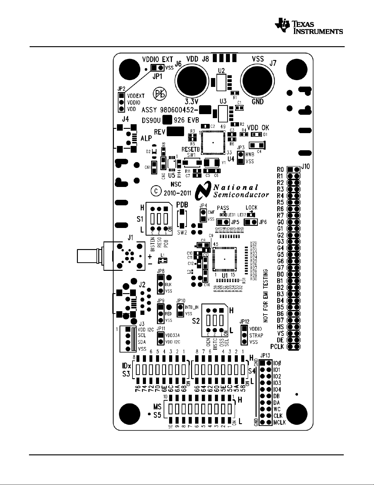
Figure 1: DS90UB926Q EVB ........................................................................................................................ 2
Figure 2: Factory Switch (S1,S2,S3,S4,S5) and Jumper (JP2) Configuration ............................................. 5
Figure 3: Initial ALP Screen .......................................................................................................................... 9
Figure 4: TOP View ..................................................................................................................................... 18
Figure 5: Bottom View ................................................................................................................................. 19
Figure 6: TOP Layer ................................................................................................................................... 20
Figure 7: GND Layer ................................................................................................................................... 21
Figure 8: PWR Layer .................................................................................................................................. 22
Figure 9: BOTTOM Layer ........................................................................................................................... 23
LIST OF TABLES
Table 1: Bill of Materials .............................................................................................................................. 29
Sept 2012 DS90UB926QSEVB User’s Guide 1
Page 2

(
)
r
(
)
www.ti.com
1. Introduction
The Texas Instruments DS90UB926QSEVB evaluation kit (EVB) provides an easy way to evaluate the
operation and performance of the DS90UB926Q 2.975Gbps FPD-Link III deserializer.
1.1. Contents of DS90UB926QSEVB
1- DS90UB926Q EVB, 1- CD with ALP software, 1- USB cable
1.2. Highlights of EVB
External 1.8V here*
Apply 3.3V here
ALP
Interface
(for register access)
FPD-Link III
Input
B
3.3V
GND
CMLOUT
Output
Monito
LVCMOS
Outputs
video
LVCMOS
I/Os
GPIOs, I2S
Figure 1: DS90UB926Q EVB
* The default factory configuration is VDDIO = 3.3V. 3.3V does not have to be applied externally. To
interface to 1.8V inputs, 1.8V must applied externally. For VDDIO = 1.8V, move jumper on JP2 to short pins 1
and 2.
2 DS90UB926QSEVB User’s Guide Sept 2012
Page 3

www.ti.com
1.3. Operation – Quick Setup
Make sure S1, S2, S3, S4, S5, and JP2 are configured as shown in Figure 1.
1) Turn on the serializer and apply PCLK.
Typically this would be the DS90UB925Q EVB.
2) If interfacing to 3.3V LVCMOS, skip this step, otherwise:
when interfacing to 1.8V LVCMOS inputs (downstream device), move factory jumper from pin-2/3 to pin 1
to connect to pin-1/2 and apply 1.8V power to pin 1 of JP1. This will connect the external 1.8V to the
DS90UB926Q VDDIO, otherwise skip this step.
3) Apply 3.3V power to the DS90UB926Q VDD.
3.3V
4) Look for the green LED2 to light up on the DS90UB926Q EVB. If the green LED is lit and stable, then the
DS90UB926Q is LOCKED to the FPD-Link III serial stream. To be absolutely sure the DS90UB926Q is
locked, use a scope to monitor off JP6 (pin 1 = LOCK, pin 2 = VSS).
CONGRATULATIONS, you are up and running!
If not continue to the next step…
1.4. Trouble Shooting the EVB
1) Check power supply polarity!!! Warning: reverse supply polarity can damage the board.
2) Check to make sure there is sufficient current by checking that the voltage (3.3V) is correct at J6.
3) Check polarity of SER to DES cable interface. e.g. SER DOUT+ is going to RIN+ of DES and vice versa.
4) Check to make sure there is a FPD-Link III signal by probing on both
5) Go back to figure 1 and double check factory settings.
Sept 2012 Literature Number: SNLU114 3
C10 AND C11.
Page 4

www.ti.com
2. Board Setup Details
This section describes, in detail, the connectors and jumpers on the board as well as how to properly
connect, set up, and use the DS90UB926Q EVB.
2.1. Power Connections
1) Connect ground to J7.
2) Connect an external 3.3V into J6. This is the core voltage of the DS90UB926Q.
3) For VDDIO = 1.8V, connect ground to pin 2 of JP1.
4) Connect an external 1.8V into pin 1 of JP1. This is VDDIO power.
2.2. FPD-Link III Connection
J12, J13 – is the default SMA connector. Apply an FPD-Link III serial stream into J12 and J13. Note: J12
goes to RxIN+, J13 goes to RxIN- of the DS90UB926Q. Typically the serializer will be the DS90UB925Q.
2.3. Factory Set Switch Settings and Jumpers Default Configuration
S1, S2, S3, S4, S5, and JP2 are factory configured as shown in Figure 2 for plug and play operation. For
each of these 3-pin headers JP2, a jumper must be placed as shown.
1)
The S1 switch is factory set as shown below.
The PDB switch is set HIGH and will turn on the DS90UB926Q upon power up.
SW2 is a momentary switch. Instead of toggling switch 1 of S1 to do a PDB toggle, press SW2 to do a
PDB toggle.
4 DS90UB926QSEVB User’s Guide Sept 2012
Page 5

www.ti.com
2) The S2 switch is factory set as shown below.
The OEN and OSS_SEL switch are set HIGH and will enable the DS90UB926Q outputs to toggle upon
power up.
3) The S3 and S4 switches are factory set as shown below.
All switches are set HIGH except 58 on S4. This sets IDx address to 58. Note only one switch is allowed
LOW at a time.
8
7
5
4) The S5 switch is factory set as shown below.
All switches are set HIGH except 1. This sets MODE_SEL address to 1. Note only one switch is allowed
LOW at a time.
5) On JP2, a 2-pin jumper is factory placed as shown below.
The jumper sets VDDIO to 3.3V. Note 3.3V does not need to be applied externally.
Figure 2: Factory Switch (S1,S2,S3,S4,S5) and Jumper (JP2) Configuration
2.4. LVCMOS Output Connector Description
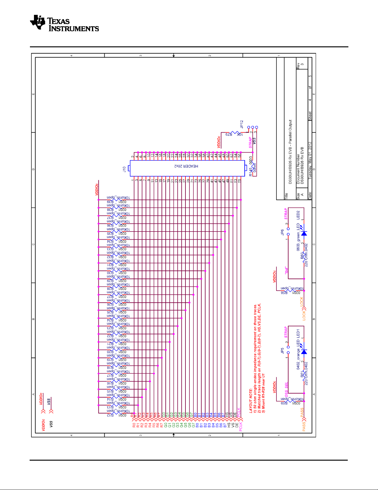
J10 – R[7:0], G[7:0], B[7:0], HS, VS, DE, PCLK is the output connector for the DS90UB926Q data outputs.
These are the LVCMOS outputs of the DS90UB926Q, which are the odd numbered pins (left side pins on the
board). The even numbered pins (right side pins on the board) go to pin 2 (labeled “STRAP”) of JP12. The
factory configuration has a jumper resistor R145 that ties the even numbered pins (STRAP) to ground.
J10 HEADER 28x 2
1 2
3 4
5 6
7 8
9 10
11 12
13 14
15 16
17 18
19 20
21 22
23 24
25 26
27 28
29 30
G0
R0
R1
R2
R3
R4
R5
R6
R7
G1
G6
G3B5G2
G5
G4
R145
0ohm
0603
31 32
33 34
35 36
37 38
39 40
41 42
43 44
45 46
47 48
49 50
51 52
53 54
55 56
G7
B0
B1
B2
B3
B4
B6
B7
HS
VS
DE
PCLK
VSS
VDD IOc
STRAP
R79
10K
JP12
1
2
3
Sept 2012 Literature Number: SNLU114 5
Page 6

www.ti.com
3. Appendix – I2C, integrated SPA Dongle
3.1. I2C SPA Dongle Hookup
Connect to PC
with supplied
USB cable
FPD-Link III
Input
B
3.3V
GND
3.2. IDx Board Default Address
The IDx address on the EVB has been preset at 58.
6 DS90UB926QSEVB User’s Guide Sept 2012
Page 7

www.ti.com
3.3. ALP Software Setup
3.3.1. System Requirements
Operating System: Windows XP or Vista
USB: 2.0
3.3.2. CD contents
Extract the “ALPF_xxxxxxxx_xxx_xxxx.exe” file to a temporary location that can
be deleted later.
Make sure J4 on the DS90UB926 is connected to a PC USB port with the
supplied USB cable and power is applied to the DS90UB926 EVB
The following installation instructions are for the Windows XP Operating System.
3.3.3. Installation of the ALP software
Execute the ALP Setup Wizard program called “ALPF_monthdayyear_major
version_minor version.exe” that was extracted to a temporary location on the local
drive of your PC.
There are 7 steps to the installation once the setup wizard is started:
1. Select the “Next” button.
2. Select “I accept the agreement” and then select the “Next” button.
3. Select the location to install the ALP software and then select the “Next” button.
4. Select the location for the start menu shortcut and then select the “Next”
button.
5. There will then be a screen that allows the creation of a desktop and Quick
Launch icon. After selecting the desired choices select the “Next” button.
6. Select the “Install” button, and the software will then be installed to the selected
location.
7. Uncheck “Launch Analog LaunchPAD” and select the “Finish” button. The ALP
software will start if “Launch Analog LaunchPAD” is checked, but it will not be
useful until the USB driver is installed.
Connect J4 of the DS90UB926Q EVB board to a PC/laptop with the supplied mini
USB cable. Power the DS90UB926Q EVB board with a 3.3 VDC power supply.
The “Found New Hardware Wizard” will open on the PC/laptop. Proceed to the
next section to install the USB driver.
Sept 2012 Literature Number: SNLU114 7
Page 8

www.ti.com
3.3.4. Installation of the USB driver
There are 6 steps to install the USB driver:
1. Select “No, not at this time” then select the “Next” button.
2. Select “Install from a list or specific location” then select the “Next” button.
3. Select “Search for the best driver in these locations”. Uncheck “Search
removable media” and check “Include this location in the search”.
4. Browse to the Install Directory which is typically located at “C:\Program
Files\National Semiconductor Corp\Analog LaunchPAD\vx.x.x\Drivers” and
select the “Next” button. Windows should find the driver.
5. Select “Continue Anyway”.
6. Select the “Finish” button.
The software installation is complete. The ALP software may now be launched, as
described in the next section.
3.3.5. Startup - Software Description
Make sure all the software has been installed and the hardware is powered on
and connected to the PC. Execute “Analog LaunchPAD” from the start menu.
The default start menu location is “Programs\National Semiconductor
Corp\Analog LaunchPAD vx.x.x\Analog LaunchPAD”.
8 DS90UB926QSEVB User’s Guide Sept 2012
Page 9

www.ti.com
The application should come up in the state shown in the figure below. If it does
not, see “Trouble Shooting” at the end of this document.
Under the Devices tab click on “DS90UB926” to select the device and open up
the device profile and its associated tabs.
Figure 3: Initial ALP Screen
After selecting the DS90UB926, the following screen should appear.
Appears only
when
deserializer is
detected
Sept 2012 Literature Number: SNLU114 9
Page 10

www.ti.com
Information Tab
The Information tab is shown below. Please note the device revision could be different.
Appears only
when
deserializer is
detected
SER Pattern Generator Tab
The SER Pattern Generator tab is shown below.
10 DS90UB926QSEVB User’s Guide Sept 2012
Page 11

www.ti.com
DES Pattern Generator Tab
The DES Pattern Generator tab is shown below.
Registers Tab
The Registers tab is shown below.
Sept 2012 Literature Number: SNLU114 11
Page 12

www.ti.com
Registers Tab – Address 0x00 selected
Address 0x00 selected as shown below. Note that the “Value:” box, , will now show the
hex value of that register.
Registers Tab – Address 0x00 expanded
By double clicking on the Address bar
or a single click on Address 0x00 expanded reveals contents by bits. Any register address
displayed can be expanded.
12 DS90UB926QSEVB User’s Guide Sept 2012
Page 13

www.ti.com
Any RW Type register, , can be written into by writing the hex value into the “Value:” box,
or putting the pointer into the individual register bit(s) box by a left mouse click to put a
check mark (indicating a “1”) or unchecking to remove the check mark (indicating a “0”). Click the
“Apply” button to write to the register, and “refresh” to see the new value of the selected
(highlighted) register.
The box toggles on every mouse click.
Scripting Tab
The Scripting tab is shown below. Usage is not described in this document.
Sept 2012 Literature Number: SNLU114 13
Page 14

www.ti.com
3.3.6. Trouble Shooting ALP Software
If the following window opens after starting the ALP software, double check the
hardware setup.
Analog LaunchPAD No Devices Error
It may also be that the USB driver is not installed. Check the device manager.
There should be an “NSC ALP Nano Atmel” device under the “Universal Serial
Bus Controllers” as shown below.
Windows XP, Analog LaunchPAD USB Driver
The software should start with only “DS90UB926Q” in the “Devices” pull down
menu. If there are more devices then the software is most likely in demo mode.
When the ALP is operating in demo mode there is a “(Demo Mode)” indication in
the lower left of the application status bar as shown below.
14 DS90UB926QSEVB User’s Guide Sept 2012
Page 15

www.ti.com
Analog LaunchPAD in Demo Mode
Disable the demo mode by selecting the “Preferences” pull down menu and unchecking “Enable Demo Mode”.
Analog LaunchPAD Preferences Menu
After demo mode is disabled, the ALP software will poll the ALP hardware. The
ALP software will update and have only “DS90UB926Q” under the “Devices” pull
down menu.
Sept 2012 Literature Number: SNLU114 15
Page 16

www.ti.com
4. Eye Monitor – CMLOP/N
CMLOP
CMLON
Top view of CML access points (upper right hand side of EVB when looking at the front side of the EVB).
Connector J15 connects CMLOP and J16 connects to CMLON.
CMLOP
CMLON
Bottom view of CML access points (upper left hand side of the EVB when looking at the back side of the
EVB).
CMLOP/N must be enabled by register, 0x56[3] = 0, to be able to monitor the FPD-Link III serial stream.
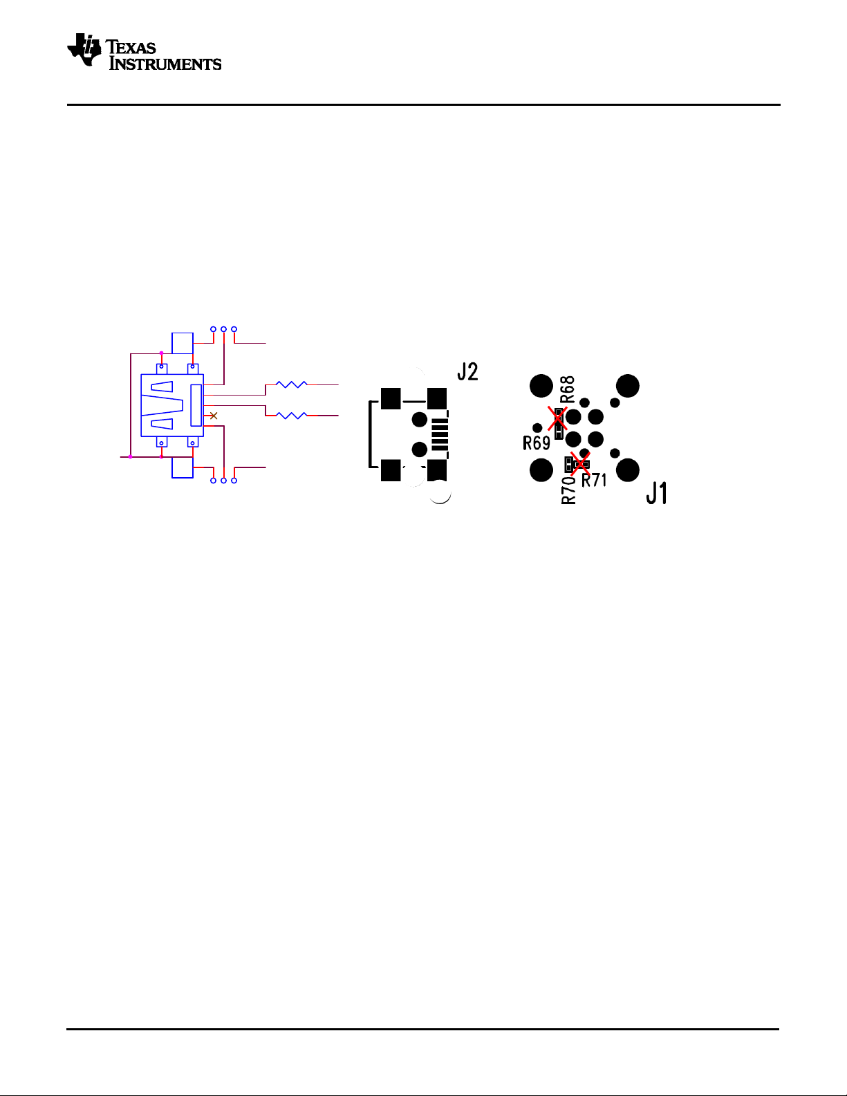
5. Appendix – Use of optional Rosenberger HSD connector (J1)
Unpopulate R68 and R71 0201 sized 0Ω resistor. R68 and R71 pads are on the back side
of the EVM. This will cut the stub traces to J12 and J13 (SMAs). Populate J1 (Rosenberger
HSD connector).
J12
RIN+_SMA
1
2
3
4
5
SMA
J13
RIN-_SMA
1
2
3
4
5
SMA
VSS
VSS
0 ohm
R71
0 ohm
0201
0201
RIN+R68
RIN-
HSD_2X2_open
9
10
1112
13
VSS
RIN+
J1
1
23
5
67
4
8
RIN-
16 DS90UB926QSEVB User’s Guide Sept 2012
Page 17
www.ti.com
6. Appendix – Use of optional mini-B USB connector (J2)
Use this option when connecting to standard DS90UR905Q EVB.
Populate R69 and R70 with 0201 sized 0Ω resistor (suggest Panasonic ERJ-1GE0R00C or
equivalent). R69 and R70 pads are on the back side of the EVM under J1. This will connect
J2. Ideally, J1 (Rosenberger HSD connector) should be removed to eliminate the stub.
Warning: R68 and R71 should not be populated when using J2.
3-Pin Header_open
VIA1
CON1
J2
9
mini USB 5pin_open
6
VSS
mini B:
component side
(TOP)
VIA2
CON1
1
1
2
3
4
5
78
1
3-Pin Header_open
JP8
VSS
123
RED
RIN+_USB
RIN-_USB
BLK
VSS
123
JP9
R69
0201
0 ohm_open
R70
0201
0 ohm_open
RIN+
RIN-
Add a two pin jumper on JP8 and JP9; this will ground the unused wires in the USB cable.
7. Appendix - Board Layout
Figure 5, Figure 6, Figure 7, and Figure 8 show the board layout for the DS90UB926Q EVB.
The DS90UB926Q is a 4-layer board (TOP / GND / PWR / BOTTOM). The 50Ω microstrip trace on the top
layer of the board is referenced to GND, and the 100Ω differential traces are referenced to GND.
Sept 2012 Literature Number: SNLU114 17
Page 18
www.ti.com
Figure 4: TOP View
18 DS90UB926QSEVB User’s Guide Sept 2012
Page 19

www.ti.com
Figure 5: Bottom View
Sept 2012 Literature Number: SNLU114 19
Page 20
www.ti.com
Figure 6: TOP Layer
20 DS90UB926QSEVB User’s Guide Sept 2012
Page 21
www.ti.com
Figure 7: GND Layer
Sept 2012 Literature Number: SNLU114 21
Page 22

www.ti.com
Figure 8: PWR Layer
22 DS90UB926QSEVB User’s Guide Sept 2012
Page 23

www.ti.com
Figure 9: BOTTOM Layer
Sept 2012 Literature Number: SNLU114 23
Page 24

www.ti.com
8. Schematic
24 DS90UB926QSEVB User’s Guide Sept 2012
Page 25

www.ti.com
Sept 2012 Literature Number: SNLU114 25
Page 26

www.ti.com
26 DS90UB926QSEVB User’s Guide Sept 2012
Page 27
www.ti.com
Sept 2012 Literature Number: SNLU114 27
Page 28

www.ti.com
28 DS90UB926QSEVB User’s Guide Sept 2012
Page 29

Schematic
9. Bill of Materials
Table 1: Bill of Materials
Sept 2012 Literature Number: SNLU114 29
Page 30

EVALUATION BOARD/KIT/MODULE (EVM) ADDITIONAL TERMS
Texas Instruments (TI) provides the enclosed Evaluation Board/Kit/Module (EVM) under the following conditions:
The user assumes all responsibility and liability for proper and safe handling of the goods. Further, the user
indemnifies TI from all claims arising from the handling or use of the goods.
Should this evaluation board/kit not meet the specifications indicated in the User’s Guide, the board/kit may be
returned within 30 days from the date of delivery for a full refund. THE FOREGOING LIMITED WARRANTY IS THE
EXCLUSIVE WARRANTY MADE BY SELLER TO BUYER AND IS IN LIEU OF ALL OTHER WARRANTIES,
EXPRESSED, IMPLIED, OR STATUTORY, INCLUDING ANY WARRANTY OF MERCHANTABILITY OR FITNESS
FOR ANY PARTICULAR PURPOSE. EXCEPT TO THE EXTENT OF THE INDEMNITY SET FORTH ABOVE,
NEITHER PARTY SHALL BE LIABLE TO THE OTHER FOR ANY INDIRECT, SPECIAL, INCIDENTAL, OR
CONSEQUENTIAL DAMAGES.
Please read the User's Guide and, specifically, the Warnings and Restrictions notice in the User's Guide prior to
handling the product. This notice contains important safety information about temperatures and voltages. For
additional information on TI's environmental and/or safety programs, please visit www.ti.com/esh or contact TI.
No license is granted under any patent right or other intellectual property right of TI covering or relating to any
machine, process, or combination in which such TI products or services might be or are used. TI currently deals
with a variety of customers for products, and therefore our arrangement with the user is not exclusive. TI assumes
no liability for applications assistance, customer product design, software performance, or infringement of patents
or services described herein.
REGULATORY COMPLIANCE INFORMATION
As noted in the EVM User’s Guide and/or EVM itself, this EVM and/or accompanying hardware may or may not be
subject to the Federal Communications Commission (FCC) and Industry Canada (IC) rules.
For EVMs not subject to the above rules, this evaluation board/kit/module is intended for use for ENGINEERING
DEVELOPMENT, DEMONSTRATION OR EVALUATION PURPOSES ONLY and is not considered by TI to be a
finished end product fit for general consumer use. It generates, uses, and can radiate radio frequency energy and
has not been tested for compliance with the limits of computing devices pursuant to part 15 of FCC or ICES-003
rules, which are designed to provide reasonable protection against radio frequency interference. Operation of the
equipment may cause interference with radio communications, in which case the user at his own expense will be
required to take whatever measures may be required to correct this interference.
General Statement for EVMs including a radio
User Power/Frequency Use Obligations: This radio is intended for development/professional use only in legally
allocated frequency and power limits. Any use of radio frequencies and/or power availability of this EVM and its
development application(s) must comply with local laws governing radio spectrum allocation and power limits for
this evaluation module. It is the user’s sole responsibility to only operate this radio in legally acceptable frequency
space and within legally mandated power limitations. Any exceptions to this are strictly prohibited and unauthorized
by Texas Instruments unless user has obtained appropriate experimental/development licenses from local
regulatory authorities, which is responsibility of user including its acceptable authorization.
For EVMs annotated as FCC – FEDERAL COMMUNICATIONS COMMISSION Part 15 Compliant
Caution
This device complies with part 15 of the FCC Rules. Operation is subject to the following two conditions: (1) This
device may not cause harmful interference, and (2) this device must accept any interference received, including
interference that may cause undesired operation.
Changes or modifications not expressly approved by the party responsible for compliance could void the user's
authority to operate the equipment.
FCC Interference Statement for Class A EVM devices
Page 31

This equipment has been tested and found to comply with the limits for a Class A digital device, pursuant to part 15
of the FCC Rules. These limits are designed to provide reasonable protection against harmful interference when
the equipment is operated in a commercial environment. This equipment generates, uses, and can radiate radio
frequency energy and, if not installed and used in accordance with the instruction manual, may cause harmful
interference to radio communications. Operation of this equipment in a residential area is likely to cause harmful
interference in which case the user will be required to correct the interference at his own expense.
FCC Interference Statement for Class B EVM devices
This equipment has been tested and found to comply with the limits for a Class B digital device, pursuant to part 15
of the FCC Rules. These limits are designed to provide reasonable protection against harmful interference in a
residential installation. This equipment generates, uses and can radiate radio frequency energy and, if not installed
and used in accordance with the instructions, may cause harmful interference to radio communications. However,
there is no guarantee that interference will not occur in a particular installation. If this equipment does cause
harmful interference to radio or television reception, which can be determined by turning the equipment off and on,
the user is encouraged to try to correct the interference by one or more of the following measures:
• Reorient or relocate the receiving antenna.
• Increase the separation between the equipment and receiver.
• Connect the equipment into an outlet on a circuit different from that to which the receiver is connected.
• Consult the dealer or an experienced radio/TV technician for help.
For EVMs annotated as IC – INDUSTRY CANADA Compliant
This Class A or B digital apparatus complies with Canadian ICES-003.
Changes or modifications not expressly approved by the party responsible for compliance could void the user’s
authority to operate the equipment.
Concerning EVMs including radio transmitters
This device complies with Industry Canada licence-exempt RSS standard(s). Operation is subject to the following
two conditions: (1) this device may not cause interference, and (2) this device must accept any interference,
including interference that may cause undesired operation of the device.
Concerning EVMs including detachable antennas
Under Industry Canada regulations, this radio transmitter may only operate using an antenna of a type and
maximum (or lesser) gain approved for the transmitter by Industry Canada. To reduce potential radio interference to
other users, the antenna type and its gain should be so chosen that the equivalent isotropically radiated power
(e.i.r.p.) is not more than that necessary for successful communication.
This radio transmitter has been approved by Industry Canada to operate with the antenna types listed in the user
guide with the maximum permissible gain and required antenna impedance for each antenna type indicated.
Antenna types not included in this list, having a gain greater than the maximum gain indicated for that type, are
strictly prohibited for use with this device.
Cet appareil numérique de la classe A ou B est conforme à la norme NMB-003 du Canada.
Les changements ou les modifications pas expressément approuvés par la partie responsable de la conformité ont
pu vider l’autorité de l'utilisateur pour actionner l'équipement.
Concernant les EVMs avec appareils radio
Le présent appareil est conforme aux CNR d'Industrie Canada applicables aux appareils radio exempts de licence.
L'exploitation est autorisée aux deux conditions suivantes : (1) l'appareil ne doit pas produire de brouillage, et (2)
l'utilisateur de l'appareil doit accepter tout brouillage radioélectrique subi, même si le brouillage est susceptible d'en
compromettre le fonctionnement.
Concernant les EVMs avec antennes détachables
Conformément à la réglementation d'Industrie Canada, le présent émetteur radio peut fonctionner avec une
antenne d'un type et d'un gain maximal (ou inférieur) approuvé pour l'émetteur par Industrie Canada. Dans le but
Page 32

de réduire les risques de brouillage radioélectrique à l'intention des autres utilisateurs, il faut choisir le type
d'antenne et son gain de sorte que la puissance isotrope rayonnée équivalente (p.i.r.e.) ne dépasse pas l'intensité
nécessaire à l'établissement d'une communication satisfaisante.
Le présent émetteur radio a été approuvé par Industrie Canada pour fonctionner avec les types d'antenne
énumérés dans le manuel d’usage et ayant un gain admissible maximal et l'impédance requise pour chaque type
d'antenne. Les types d'antenne non inclus dans cette liste, ou dont le gain est supérieur au gain maximal indiqué,
sont strictement interdits pour l'exploitation de l'émetteur.
SPACER
SPACER
SPACER
【Important Notice for Users of this Product in Japan】
This development kit is NOT certified as Confirming to Technical Regulations of Radio Law of Japan
If you use this product in Japan, you are required by Radio Law of Japan to follow the instructions below with
respect to this product:
1. Use this product in a shielded room or any other test facility as defined in the notification #173 issued by
Ministry of Internal Affairs and Communications on March 28, 2006, based on Sub-section 1.1 of Article 6
of the Ministry’s Rule for Enforcement of Radio Law of Japan,
2. Use this product only after you obtained the license of Test Radio Station as provided in Radio Law of
Japan with respect to this product, or
3. Use of this product only after you obtained the Technical Regulations Conformity Certification as provided
in Radio Law of Japan with respect to this product. Also, please do not transfer this product, unless you
give the same notice above to the transferee. Please note that if you could not follow the instructions
above, you will be subject to penalties of Radio Law of Japan.
Texas Instruments Japan Limited
(address) 24-1, Nishi-Shinjuku 6 chome, Shinjuku-ku, Tokyo, Japan
http://www.tij.co.jp
【ご使用にあたっての注】
本開発キットは技術基準適合証明を受けておりません。
本製品のご使用に際しては、電波法遵守のため、以下のいずれかの措置を取っていただく必要がありますのでご注
意ください。
1. 電波法施行規則第6条第1項第1号に基づく平成18年3月28日総務省告示第173号で定められた電波暗室等の
試験設備でご使用いただく。
2. 実験局の免許を取得後ご使用いただく。
3. 技術基準適合証明を取得後ご使用いただく。
なお、本製品は、上記の「ご使用にあたっての注意」を譲渡先、移転先に通知しない限り、譲渡、移転できないも
のとします。
上記を遵守頂けない場合は、電波法の罰則が適用される可能性があることをご留意ください。
日本テキサス・インスツルメンツ株式会社
東京都新宿区西新宿6丁目24番1号
西新宿三井ビル
http://www.tij.co.jp
SPACER
SPACER
Page 33

EVALUATION BOARD/KIT/MODULE (EVM)
WARNINGS, RESTRICTIONS AND DISCLAIMERS
For Feasibility Evaluation Only, in Laboratory/Development Environments. Unless otherwise indicated, this
EVM is not a finished electrical equipment and not intended for consumer use. It is intended solely for use for
preliminary feasibility evaluation in laboratory/development environments by technically qualified electronics experts
who are familiar with the dangers and application risks associated with handling electrical mechanical components,
systems and subsystems. It should not be used as all or part of a finished end product.
Your Sole Responsibility and Risk. You acknowledge, represent and agree that:
1. You have unique knowledge concerning Federal, State and local regulatory requirements (including but not
limited to Food and Drug Administration regulations, if applicable) which relate to your products and which
relate to your use (and/or that of your employees, affiliates, contractors or designees) of the EVM for
evaluation, testing and other purposes.
2. You have full and exclusive responsibility to assure the safety and compliance of your products with all
such laws and other applicable regulatory requirements, and also to assure the safety of any activities to be
conducted by you and/or your employees, affiliates, contractors or designees, using the EVM. Further, you
are responsible to assure that any interfaces (electronic and/or mechanical) between the EVM and any
human body are designed with suitable isolation and means to safely limit accessible leakage currents to
minimize the risk of electrical shock hazard.
3. You will employ reasonable safeguards to ensure that your use of the EVM will not result in any property
damage, injury or death, even if the EVM should fail to perform as described or expected.
4. You will take care of proper disposal and recycling of the EVM’s electronic components and packing
materials.
Certain Instructions. It is important to operate this EVM within TI’s recommended specifications and
environmental considerations per the user guidelines. Exceeding the specified EVM ratings (including but not
limited to input and output voltage, current, power, and environmental ranges) may cause property damage,
personal injury or death. If there are questions concerning these ratings please contact a TI field representative
prior to connecting interface electronics including input power and intended loads. Any loads applied outside of the
specified output range may result in unintended and/or inaccurate operation and/or possible permanent damage to
the EVM and/or interface electronics. Please consult the EVM User's Guide prior to connecting any load to the EVM
output. If there is uncertainty as to the load specification, please contact a TI field representative. During normal
operation, some circuit components may have case temperatures greater than 60°C as long as the input and output
are maintained at a normal ambient operating temperature. These components include but are not limited to linear
regulators, switching transistors, pass transistors, and current sense resistors which can be identified using the
EVM schematic located in the EVM User's Guide. When placing measurement probes near these devices during
normal operation, please be aware that these devices may be very warm to the touch. As with all electronic
evaluation tools, only qualified personnel knowledgeable in electronic measurement and diagnostics normally found
in development environments should use these EVMs.
Agreement to Defend, Indemnify and Hold Harmless. You agree to defend, indemnify and hold TI, its licensors
and their representatives harmless from and against any and all claims, damages, losses, expenses, costs and
liabilities (collectively, "Claims") arising out of or in connection with any use of the EVM that is not in accordance
with the terms of the agreement. This obligation shall apply whether Claims arise under law of tort or contract or
any other legal theory, and even if the EVM fails to perform as described or expected.
Safety-Critical or Life-Critical Applications. If you intend to evaluate the components for possible use in safety
critical applications (such as life support) where a failure of the TI product would reasonably be expected to cause
severe personal injury or death, such as devices which are classified as FDA Class III or similar classification, then
you must specifically notify TI of such intent and enter into a separate Assurance and Indemnity Agreement.
Mailing Address: Texas Instruments, Post Office Box 655303, Dallas, Texas 75265
Copyright © 2012, Texas Instruments Incorporated
Page 34

IMPORTANT NOTICE FOR TI REFERENCE DESIGNS
Texas Instruments Incorporated ("TI") reference designs are solely intended to assist designers (“Buyers”) who are developing systems that
incorporate TI semiconductor products (also referred to herein as “components”). Buyer understands and agrees that Buyer remains
responsible for using its independent analysis, evaluation and judgment in designing Buyer’s systems and products.
TI reference designs have been created using standard laboratory conditions and engineering practices. TI has not conducted any
testing other than that specifically described in the published documentation for a particular reference design. TI may make
corrections, enhancements, improvements and other changes to its reference designs.
Buyers are authorized to use TI reference designs with the TI component(s) identified in each particular reference design and to modify the
reference design in the development of their end products. HOWEVER, NO OTHER LICENSE, EXPRESS OR IMPLIED, BY ESTOPPEL
OR OTHERWISE TO ANY OTHER TI INTELLECTUAL PROPERTY RIGHT, AND NO LICENSE TO ANY THIRD PARTY TECHNOLOGY
OR INTELLECTUAL PROPERTY RIGHT, IS GRANTED HEREIN, including but not limited to any patent right, copyright, mask work right,
or other intellectual property right relating to any combination, machine, or process in which TI components or services are used.
Information published by TI regarding third-party products or services does not constitute a license to use such products or services, or a
warranty or endorsement thereof. Use of such information may require a license from a third party under the patents or other intellectual
property of the third party, or a license from TI under the patents or other intellectual property of TI.
TI REFERENCE DESIGNS ARE PROVIDED "AS IS". TI MAKES NO WARRANTIES OR REPRESENTATIONS WITH REGARD TO THE
REFERENCE DESIGNS OR USE OF THE REFERENCE DESIGNS, EXPRESS, IMPLIED OR STATUTORY, INCLUDING ACCURACY OR
COMPLETENESS. TI DISCLAIMS ANY WARRANTY OF TITLE AND ANY IMPLIED WARRANTIES OF MERCHANTABILITY, FITNESS
FOR A PARTICULAR PURPOSE, QUIET ENJOYMENT, QUIET POSSESSION, AND NON-INFRINGEMENT OF ANY THIRD PARTY
INTELLECTUAL PROPERTY RIGHTS WITH REGARD TO TI REFERENCE DESIGNS OR USE THEREOF. TI SHALL NOT BE LIABLE
FOR AND SHALL NOT DEFEND OR INDEMNIFY BUYERS AGAINST ANY THIRD PARTY INFRINGEMENT CLAIM THAT RELATES TO
OR IS BASED ON A COMBINATION OF COMPONENTS PROVIDED IN A TI REFERENCE DESIGN. IN NO EVENT SHALL TI BE
LIABLE FOR ANY ACTUAL, SPECIAL, INCIDENTAL, CONSEQUENTIAL OR INDIRECT DAMAGES, HOWEVER CAUSED, ON ANY
THEORY OF LIABILITY AND WHETHER OR NOT TI HAS BEEN ADVISED OF THE POSSIBILITY OF SUCH DAMAGES, ARISING IN
ANY WAY OUT OF TI REFERENCE DESIGNS OR BUYER’S USE OF TI REFERENCE DESIGNS.
TI reserves the right to make corrections, enhancements, improvements and other changes to its semiconductor products and services per
JESD46, latest issue, and to discontinue any product or service per JESD48, latest issue. Buyers should obtain the latest relevant
information before placing orders and should verify that such information is current and complete. All semiconductor products are sold
subject to TI’s terms and conditions of sale supplied at the time of order acknowledgment.
TI warrants performance of its components to the specifications applicable at the time of sale, in accordance with the warranty in TI’s terms
and conditions of sale of semiconductor products. Testing and other quality control techniques for TI components are used to the extent TI
deems necessary to support this warranty. Except where mandated by applicable law, testing of all parameters of each component is not
necessarily performed.
TI assumes no liability for applications assistance or the design of Buyers’ products. Buyers are responsible for their products and
applications using TI components. To minimize the risks associated with Buyers’ products and applications, Buyers should provide
adequate design and operating safeguards.
Reproduction of significant portions of TI information in TI data books, data sheets or reference designs is permissible only if reproduction is
without alteration and is accompanied by all associated warranties, conditions, limitations, and notices. TI is not responsible or liable for
such altered documentation. Information of third parties may be subject to additional restrictions.
Buyer acknowledges and agrees that it is solely responsible for compliance with all legal, regulatory and safety-related requirements
concerning its products, and any use of TI components in its applications, notwithstanding any applications-related information or support
that may be provided by TI. Buyer represents and agrees that it has all the necessary expertise to create and implement safeguards that
anticipate dangerous failures, monitor failures and their consequences, lessen the likelihood of dangerous failures and take appropriate
remedial actions. Buyer will fully indemnify TI and its representatives against any damages arising out of the use of any TI components in
Buyer’s safety-critical applications.
In some cases, TI components may be promoted specifically to facilitate safety-related applications. With such components, TI’s goal is to
help enable customers to design and create their own end-product solutions that meet applicable functional safety standards and
requirements. Nonetheless, such components are subject to these terms.
No TI components are authorized for use in FDA Class III (or similar life-critical medical equipment) unless authorized officers of the parties
have executed an agreement specifically governing such use.
Only those TI components that TI has specifically designated as military grade or “enhanced plastic” are designed and intended for use in
military/aerospace applications or environments. Buyer acknowledges and agrees that any military or aerospace use of TI components that
have not been so designated is solely at Buyer's risk, and Buyer is solely responsible for compliance with all legal and regulatory
requirements in connection with such use.
TI has specifically designated certain components as meeting ISO/TS16949 requirements, mainly for automotive use. In any case of use of
non-designated products, TI will not be responsible for any failure to meet ISO/TS16949.
Mailing Address: Texas Instruments, Post Office Box 655303, Dallas, Texas 75265
Copyright © 2014, Texas Instruments Incorporated
Page 35

Mouser Electronics
Authorized Distributor
Click to View Pricing, Inventory, Delivery & Lifecycle Information:
Texas Instruments:
DS90UB926QSEVB/NOPB DS90UB926QSEVB
 Loading...