

DS90LT012A, DS90LV012A
www.ti.com
DS90LV012A /DS90LT012A 3V LVDS Single CMOS Differential Line Receiver
Check for Samples: DS90LT012A, DS90LV012A
1
FEATURES
2
• Compatible with ANSI TIA/EIA-644-A Standard
• >400 Mbps (200 MHz) switching rates
• 100 ps differential skew (typical)
• 3.5 ns maximum propagation delay
• Integrated line termination resistor (102Ω
typical)
• Single 3.3V power supply design (2.7V to 3.6V
range)
• Power down high impedance on LVDS inputs
• Accepts small swing (350 mV typical)
differential signal levels
• LVDS receiver inputs accept
LVDS/BLVDS/LVPECL inputs
• Supports open, short and terminated input failsafe
• Pinout simplifies PCB layout
• Low Power Dissipation (10mW typical@ 3.3V
static)
• SOT-23 5-lead package
• Leadless WSON-8 package (3x3 mm body size)
• Electrically similar to the DS90LV018A
• Fabricated with advanced CMOS process
technology
• Industrial temperature operating range (−40°C
to +85°C)
SNLS141D –AUGUST 2002–REVISED APRIL 2013
DESCRIPTION
The DS90LV012A and DS90LT012A are single
CMOS differential line receivers designed for
applications requiring ultra low power dissipation, low
noise, and high data rates. The devices are designed
to support data rates in excess of 400 Mbps (200
MHz) utilizing Low Voltage Differential Swing (LVDS)
technology
The DS90LV012A and DS90LT012A accept low
voltage (350 mV typical) differential input signals and
translates them to 3V CMOS output levels. The
receivers also support open, shorted, and terminated
(100Ω) input fail-safe. The receiver output will be
HIGH for all fail-safe conditions. The DS90LV012A
has a pinout designed for easy PCB layout. The
DS90LT012A includes an input line termination
resistor for point-to-point applications.
The DS90LV012A and DS90LT012A, and companion
LVDS line driver provide a new alternative to high
power PECL/ECL devices for high speed interface
applications.
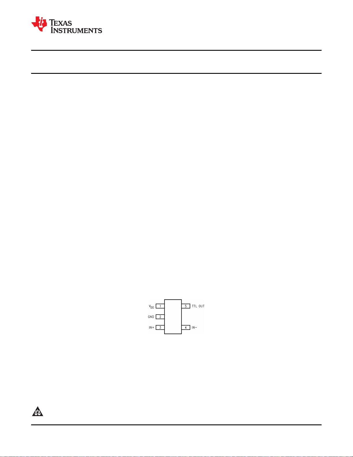
Connection Diagram
See Package Number DBV (R-PDSO-G5)
1
Please be aware that an important notice concerning availability, standard warranty, and use in critical applications of
Texas Instruments semiconductor products and disclaimers thereto appears at the end of this data sheet.
2All trademarks are the property of their respective owners.
PRODUCTION DATA information is current as of publication date.
Products conform to specifications per the terms of the Texas
Instruments standard warranty. Production processing does not
necessarily include testing of all parameters.
Figure 1. Top View
Copyright © 2002–2013, Texas Instruments Incorporated
DS90LT012A, DS90LV012A
SNLS141D –AUGUST 2002–REVISED APRIL 2013
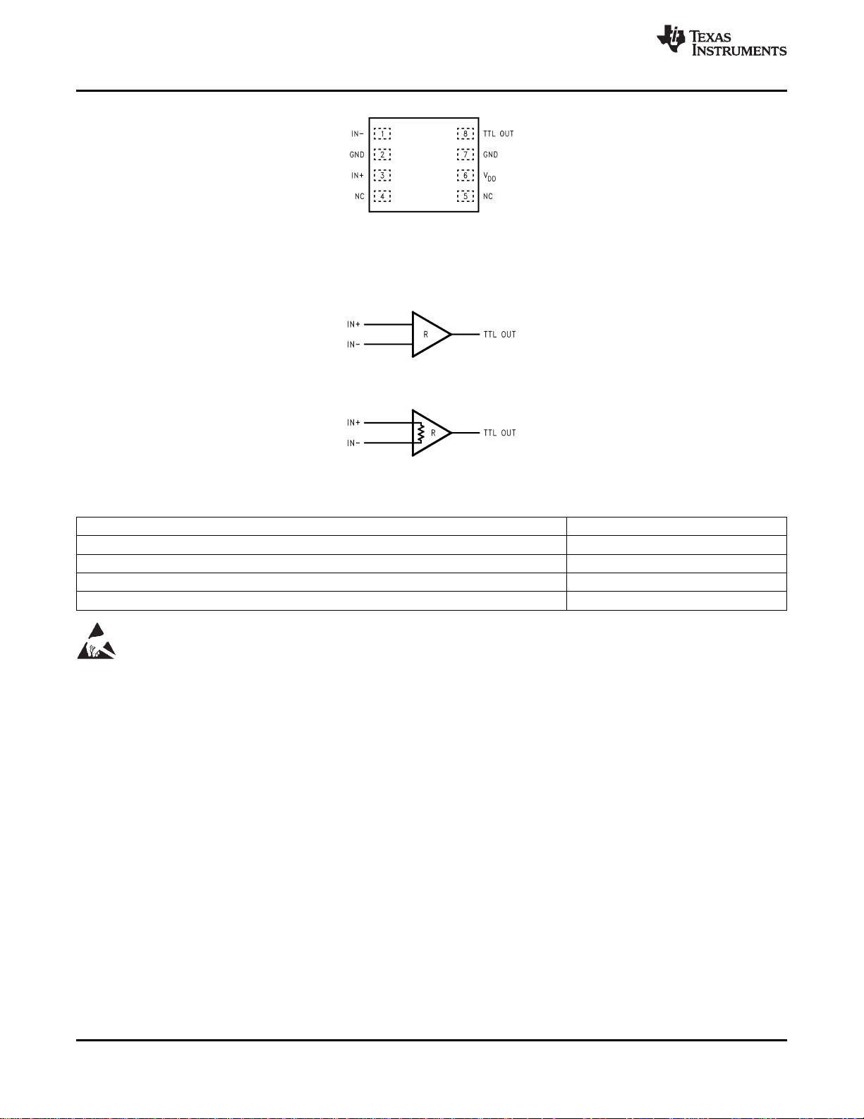
Functional Diagram
www.ti.com
Figure 2. Top View
See Package Number NGK0008A
Figure 3. DS90LV012A
Figure 4. DS90LT012A
Truth Table
INPUTS OUTPUT
[IN+] − [IN−] TTL OUT
VID≥ 0V H
VID≤ −0.1V L
Full Fail-safe OPEN/SHORT or Terminated H
These devices have limited built-in ESD protection. The leads should be shorted together or the device placed in conductive foam
during storage or handling to prevent electrostatic damage to the MOS gates.
2 Submit Documentation Feedback Copyright © 2002–2013, Texas Instruments Incorporated
Product Folder Links: DS90LT012A DS90LV012A
DS90LT012A, DS90LV012A
www.ti.com
Absolute Maximum Ratings
Supply Voltage (VDD) −0.3V to +4V
Input Voltage (IN+, IN−) −0.3V to +3.9V
Output Voltage (TTL OUT) −0.3V to (VDD+ 0.3V)
Output Short Circuit Current −100mA
Maximum Package Power Dissipation @ +25°C
NGK Package 2.26 W
Derate NGK Package 18.1 mW/°C above +25°C
Thermal resistance (θJA) 55.3°C/W
DBV Package 902mW
Derate DBV Package 7.22 mW/°C above +25°C
Thermal resistance (θJA) 138.5°C/W
Storage Temperature Range −65°C to +150°C
Lead Temperature Range Soldering (4 sec.) +260°C
Maximum Junction Temperature +150°C
ESD Ratings
(1) “Absolute Maximum Ratings” are those values beyond which the safety of the device cannot be ensured. They are not meant to imply
that the devices should be operated at these limits. Electrical Characteristics specifies conditions of device operation.
(2) ESD Ratings:
(a) DS90LV012A:
(b) DS90LT012A:
(2)
(a) HBM (1.5 kΩ, 100 pF) ≥ 2kV
(b) EIAJ (0Ω, 200 pF) ≥ 900V
(c) CDM ≥ 2000V
(d) IEC direct (330Ω, 150 pF) ≥ 5kV
(a) HBM (1.5 kΩ, 100 pF) ≥ 2kV
(b) EIAJ (0Ω, 200 pF) ≥ 700V
(c) CDM ≥ 2000V
(d) IEC direct (330Ω, 150 pF) ≥ 7kV
(1)
SNLS141D –AUGUST 2002–REVISED APRIL 2013
Recommended Operating Conditions
Min Typ Max Units
Supply Voltage (VDD) +2.7 +3.3 +3.6 V
Operating Free Air Temperature (TA) −40 25 +85 °C
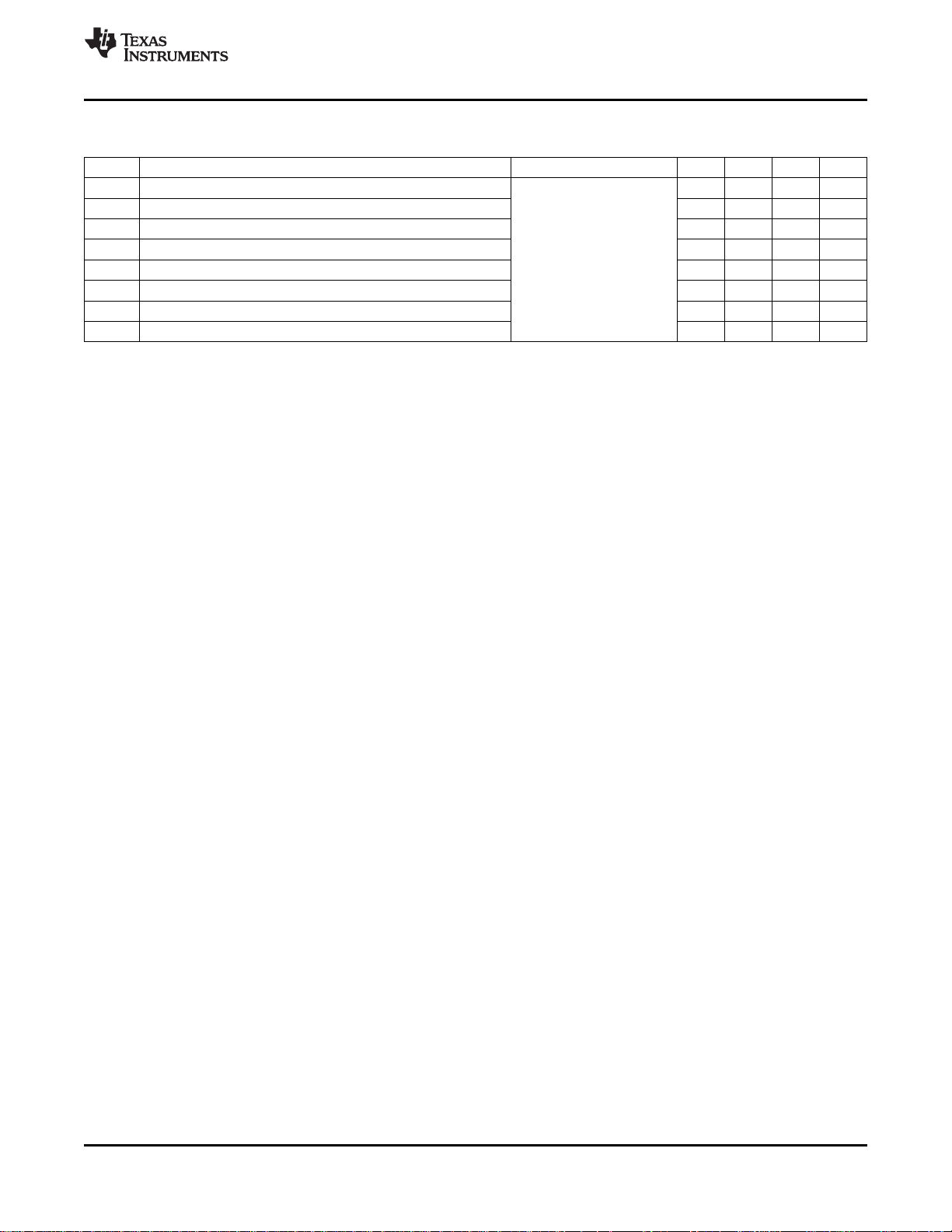
Electrical Characteristics
Over Supply Voltage and Operating Temperature ranges, unless otherwise specified.
(1) Current into device pins is defined as positive. Current out of device pins is defined as negative. All voltages are referenced to ground
unless otherwise specified (such as VID).
(2) All typicals are given for: VDD= +3.3V and TA= +25°C.
Copyright © 2002–2013, Texas Instruments Incorporated Submit Documentation Feedback 3
Product Folder Links: DS90LT012A DS90LV012A
(1) (2)
DS90LT012A, DS90LV012A
SNLS141D –AUGUST 2002–REVISED APRIL 2013
www.ti.com
Electrical Characteristics (continued)
Over Supply Voltage and Operating Temperature ranges, unless otherwise specified.
Symbol Parameter Conditions Pin Min Typ Max Units
IN−
IN−
(3)
DD
= +0V
= +2.0V
V
V
V
Differential Input High Threshold VCMdependant on V
TH
Differential Input Low Threshold −100 −30 mV
TL
Common-Mode Voltage VDD= 2.7V, VID= 100mV 0.05 2.35 V
CM
VDD= 3.0V to 3.6V, VID= 100mV 0.05 VDD- 0.3V V
I
IN
Input Current (DS90LV012A) VIN= +2.8V VDD= 3.6V or 0V −10 ±1 +10 μA
VIN= 0V −10 ±1 +10 μA
VIN= +3.6V VDD= 0V −20 +20 μA
ΔI
Change in Magnitude of I
IN
IN
VIN= +2.8V VDD= 3.6V or 0V 4 μA
VIN= 0V 4 μA
VIN= +3.6V VDD= 0V 4 μA
I
R
C
V
IND
Differential Input Current V
(DS90LT012A) V
Integrated Termination Resistor
T
(DS90LT012A)
Input Capacitance IN+ = IN− = GND 3 pF
IN
Output High Voltage IOH= −0.4 mA, VID= +200 mV TTL OUT 2.4 3.1 V
OH
= +0.4V, V
IN+
= +2.4V, V
IN+
IOH= −0.4 mA, Inputs terminated 2.4 3.1 V
IOH= −0.4 mA, Inputs shorted 2.4 3.1 V
V
I
OS
V
I
DD
Output Low Voltage IOL= 2 mA, VID= −200 mV 0.3 0.5 V
OL
Output Short Circuit Current V
Input Clamp Voltage ICL= −18 mA −1.5 −0.7 V
CL
OUT
= 0V
(4)
No Load Supply Current Inputs Open V
(3) VDDis always higher than IN+ and IN− voltage. IN+ and IN− are allowed to have voltage range −0.05V to +2.35V when VDD= 2.7V and
|VID| / 2 to VDD− 0.3V when VDD= 3.0V to 3.6V. VIDis not allowed to be greater than 100 mV when VCM= 0.05V to 2.35V when VDD=
2.7V or when VCM= |VID| / 2 to VDD− 0.3V when VDD= 3.0V to 3.6V.
(4) Output short circuit current (IOS) is specified as magnitude only, minus sign indicates direction only. Only one output should be shorted
at a time, do not exceed maximum junction temperature specification.
(1) (2)
IN+, IN− −30 0 mV
3 3.9 4.4 mA
102 Ω
−15 −50 −100 mA
DD
5.4 9 mA
4 Submit Documentation Feedback Copyright © 2002–2013, Texas Instruments Incorporated
Product Folder Links: DS90LT012A DS90LV012A
DS90LT012A, DS90LV012A
www.ti.com
SNLS141D –AUGUST 2002–REVISED APRIL 2013
Switching Characteristics
Over Supply Voltage and Operating Temperature ranges, unless otherwise specified.
Symbol Parameter Conditions Min Typ Max Units
t
PHLD
t
PLHD
t
SKD1
t
SKD3
t
SKD4
t
TLH
t
THL
f
MAX
(1) CLincludes probe and jig capacitance.
(2) Generator waveform for all tests unless otherwise specified: f = 1 MHz, ZO= 50Ω, trand tf(0% to 100%) ≤ 3 ns for IN±.
(3) t
(4) t
(5) t
(6) f
Differential Propagation Delay High to Low CL= 15 pF 1.0 1.8 3.5 ns
Differential Propagation Delay Low to High VID= 200 mV 1.0 1.7 3.5 ns
Differential Pulse Skew |t
PHLD
Differential Part to Part Skew
Differential Part to Part Skew
− t
(4)
(5)
PLHD
(3)
|
(Figure 5 and Figure 6) 0 100 400 ps
Rise Time 350 800 ps
Fall Time 175 800 ps
Maximum Operating Frequency
is the magnitude difference in differential propagation delay time between the positive-going-edge and the negative-going-edge of
SKD1
the same channel.
, part to part skew, is the differential channel-to-channel skew of any event between devices. This specification applies to devices
SKD3
at the same VDDand within 5°C of each other within the operating temperature range.
, part to part skew, is the differential channel-to-channel skew of any event between devices. This specification applies to devices
SKD4
over the recommended operating temperature and voltage ranges, and across process distribution. t
(6)
differential propagation delay.
generator input conditions: tr= tf< 1 ns (0% to 100%), 50% duty cycle, differential (1.05V to 1.35 peak to peak). Output criteria:
MAX
60%/40% duty cycle, VOL(max 0.4V), VOH(min 2.4V), load = 15 pF (stray plus probes). The parameter is ensured by design. The limit
is based on the statistical analysis of the device over the PVT range by the transition times (t
(1) (2)
TLH
0 0.3 1.0 ns
0 0.4 1.5 ns
200 250 MHz
is defined as |Max − Min|
SKD4
and t
).
THL
Copyright © 2002–2013, Texas Instruments Incorporated Submit Documentation Feedback 5
Product Folder Links: DS90LT012A DS90LV012A
DS90LT012A, DS90LV012A
SNLS141D –AUGUST 2002–REVISED APRIL 2013
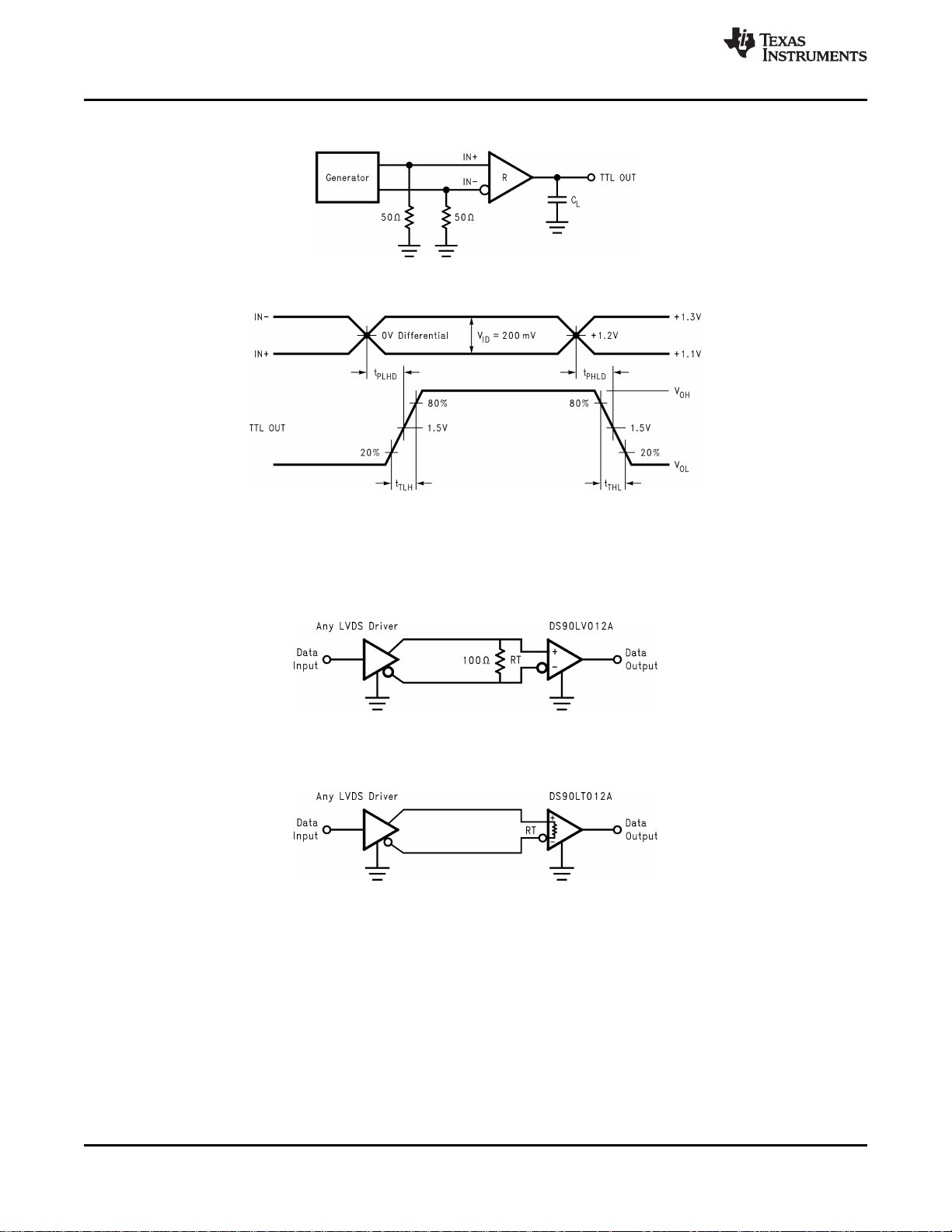
PARAMETER MEASUREMENT INFORMATION
Figure 5. Receiver Propagation Delay and Transition Time Test Circuit
Figure 6. Receiver Propagation Delay and Transition Time Waveforms
www.ti.com
TYPICAL APPLICATIONS
Balanced System
Figure 7. Point-to-Point Application (DS90LV012A)
Balanced System
Figure 8. Point-to-Point Application (DS90LT012A)
6 Submit Documentation Feedback Copyright © 2002–2013, Texas Instruments Incorporated
Product Folder Links: DS90LT012A DS90LV012A

DS90LT012A, DS90LV012A
www.ti.com
SNLS141D –AUGUST 2002–REVISED APRIL 2013
APPLICATION INFORMATION
General application guidelines and hints for LVDS drivers and receivers may be found in the following application
notes: LVDS Owner's Manual (SNLA187), AN-808 (SNLA028), AN-977 (SNLA166), AN-971 (SNLA165), AN-916
(SNLA219), AN-805 (SNOA233), AN-903 (SNLA034).
LVDS drivers and receivers are intended to be primarily used in an uncomplicated point-to-point configuration as
is shown in Figure 7. This configuration provides a clean signaling environment for the fast edge rates of the
drivers. The receiver is connected to the driver through a balanced media which may be a standard twisted pair
cable, a parallel pair cable, or simply PCB traces. Typically the characteristic impedance of the media is in the
range of 100Ω. A termination resistor of 100Ω should be selected to match the media, and is located as close to
the receiver input pins as possible. The termination resistor converts the driver output (current mode) into a
voltage that is detected by the receiver. Other configurations are possible such as a multi-receiver configuration,
but the effects of a mid-stream connector(s), cable stub(s), and other impedance discontinuities as well as
ground shifting, noise margin limits, and total termination loading must be taken into account.
The DS90LV012A and DS90LT012A differential line receivers are capable of detecting signals as low as 100
mV, over a ±1V common-mode range centered around +1.2V. This is related to the driver offset voltage which is
typically +1.2V. The driven signal is centered around this voltage and may shift ±1V around this center point. The
±1V shifting may be the result of a ground potential difference between the driver's ground reference and the
receiver's ground reference, the common-mode effects of coupled noise, or a combination of the two. The AC
parameters of both receiver input pins are optimized for a recommended operating input voltage range of 0V to
+2.4V (measured from each pin to ground). The device will operate for receiver input voltages up to VDD, but
exceeding VDDwill turn on the ESD protection circuitry which will clamp the bus voltages.
POWER DECOUPLING RECOMMENDATIONS
Bypass capacitors must be used on power pins. Use high frequency ceramic (surface mount is recommended)
0.1μF and 0.001μF capacitors in parallel at the power supply pin with the smallest value capacitor closest to the
device supply pin. Additional scattered capacitors over the printed circuit board will improve decoupling. Multiple
vias should be used to connect the decoupling capacitors to the power planes. A 10μF (35V) or greater solid
tantalum capacitor should be connected at the power entry point on the printed circuit board between the supply
and ground.
PC BOARD CONSIDERATIONS
Use at least 4 PCB board layers (top to bottom): LVDS signals, ground, power, TTL signals.
Isolate TTL signals from LVDS signals, otherwise the TTL signals may couple onto the LVDS lines. It is best to
put TTL and LVDS signals on different layers which are isolated by a power/ground plane(s).
Keep drivers and receivers as close to the (LVDS port side) connectors as possible.
For PC board considerations for the WSON package, please refer to application note AN-1187 “Leadless
Leadframe Package” (SNOA401). It is important to note that to optimize signal integrity (minimize jitter and noise
coupling), the WSON thermal land pad, which is a metal (normally copper) rectangular region located under the
package, should be attached to ground and match the dimensions of the exposed pad on the PCB (1:1 ratio).
DIFFERENTIAL TRACES
Use controlled impedance traces which match the differential impedance of your transmission medium (ie. cable)
and termination resistor. Run the differential pair trace lines as close together as possible as soon as they leave
the IC (stubs should be < 10mm long). This will help eliminate reflections and ensure noise is coupled as
common-mode. In fact, we have seen that differential signals which are 1mm apart radiate far less noise than
traces 3mm apart since magnetic field cancellation is much better with the closer traces. In addition, noise
induced on the differential lines is much more likely to appear as common-mode which is rejected by the
receiver.
Match electrical lengths between traces to reduce skew. Skew between the signals of a pair means a phase
difference between signals which destroys the magnetic field cancellation benefits of differential signals and EMI
will result! (Note that the velocity of propagation, v = c/Erwhere c (the speed of light) = 0.2997mm/ps or 0.0118
in/ps). Do not rely solely on the autoroute function for differential traces. Carefully review dimensions to match
differential impedance and provide isolation for the differential lines. Minimize the number of vias and other
discontinuities on the line.
Copyright © 2002–2013, Texas Instruments Incorporated Submit Documentation Feedback 7
Product Folder Links: DS90LT012A DS90LV012A
DS90LT012A, DS90LV012A
SNLS141D –AUGUST 2002–REVISED APRIL 2013
www.ti.com
Avoid 90° turns (these cause impedance discontinuities). Use arcs or 45° bevels.
Within a pair of traces, the distance between the two traces should be minimized to maintain common-mode
rejection of the receivers. On the printed circuit board, this distance should remain constant to avoid
discontinuities in differential impedance. Minor violations at connection points are allowable.
TERMINATION
DS90LV012A:
Use a termination resistor which best matches the differential impedance or your transmission line. The resistor
should be between 90Ω and 130Ω. Remember that the current mode outputs need the termination resistor to
generate the differential voltage. LVDS will not work without resistor termination. Typically, connecting a single
resistor across the pair at the receiver end will suffice.
Surface mount 1% - 2% resistors are the best. PCB stubs, component lead, and the distance from the
termination to the receiver inputs should be minimized. The distance between the termination resistor and the
receiver should be < 10mm (12mm MAX).
DS90LT012A:
The DS90LT012A integrates the terminating resistor for point-to-point applications. The resistor value will be
between 90Ω and 133Ω.
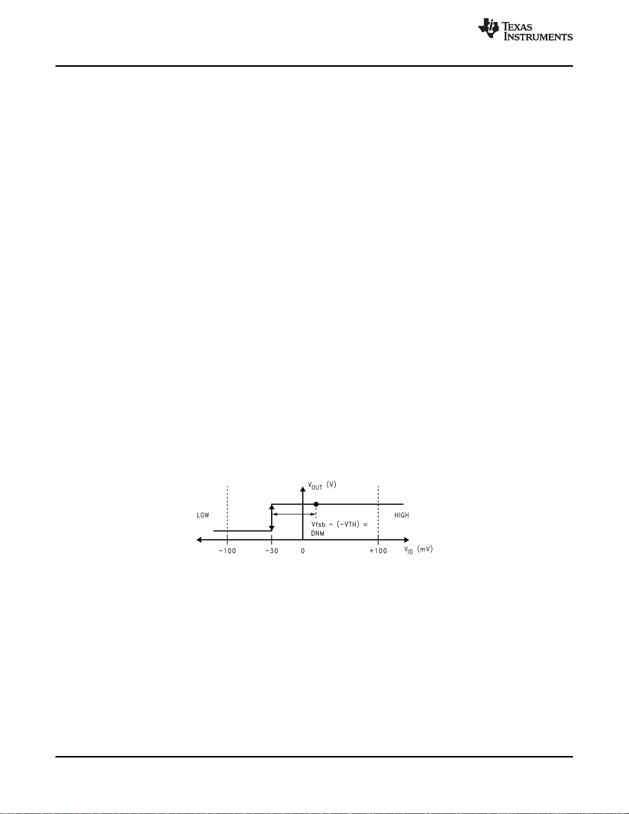
THRESHOLD
The LVDS Standard (ANSI/TIA/EIA-644-A) specifies a maximum threshold of ±100mV for the LVDS receiver.
The DS90LV012A and DS90LT012A support an enhanced threshold region of −100mV to 0V. This is useful for
fail-safe biasing. The threshold region is shown in the Voltage Transfer Curve (VTC) in Figure 9. The typical
DS90LV012A or DS90LT012A LVDS receiver switches at about −30mV. Note that with VID= 0V, the output will
be in a HIGH state. With an external fail-safe bias of +25mV applied, the typical differential noise margin is now
the difference from the switch point to the bias point. In the example below, this would be 55mV of Differential
Noise Margin (+25mV − (−30mV)). With the enhanced threshold region of −100mV to 0V, this small external failsafe biasing of +25mV (with respect to 0V) gives a DNM of a comfortable 55mV. With the standard threshold
region of ±100mV, the external fail-safe biasing would need to be +25mV with respect to +100mV or +125mV,
giving a DNM of 155mV which is stronger fail-safe biasing than is necessary for the DS90LV012A or
DS90LT012A. If more DNM is required, then a stronger fail-safe bias point can be set by changing resistor
values.
Figure 9. VTC of the DS90LV012A and DS90LT012A LVDS Receivers
8 Submit Documentation Feedback Copyright © 2002–2013, Texas Instruments Incorporated
Product Folder Links: DS90LT012A DS90LV012A

DS90LT012A, DS90LV012A
www.ti.com
SNLS141D –AUGUST 2002–REVISED APRIL 2013
FAIL-SAFE FEATURE
The LVDS receiver is a high gain, high speed device that amplifies a small differential signal (20mV) to CMOS
logic levels. Due to the high gain and tight threshold of the receiver, care should be taken to prevent noise from
appearing as a valid signal.
The receiver's internal fail-safe circuitry is designed to source/sink a small amount of current, providing fail-safe
protection (a stable known state of HIGH output voltage) for floating, terminated or shorted receiver inputs.
1. Open Input Pins. The DS90LV012A and DS90LT012A are single receiver devices. It is not required to tie
the receiver inputs to ground or any supply voltage. Internal failsafe circuitry will ensure a HIGH, stable
output state for open inputs.
2. Terminated Input. If the driver is disconnected (cable unplugged), or if the driver is in a power-off condition,
the receiver output will again be in a HIGH state, even with the end of cable 100Ω termination resistor across
the input pins. The unplugged cable can become a floating antenna which can pick up noise. If the cable
picks up more than 10mV of differential noise, the receiver may see the noise as a valid signal and switch.
To insure that any noise is seen as common-mode and not differential, a balanced interconnect should be
used. Twisted pair cable will offer better balance than flat ribbon cable.
3. Shorted Inputs. If a fault condition occurs that shorts the receiver inputs together, thus resulting in a 0V
differential input voltage, the receiver output will remain in a HIGH state. Shorted input fail-safe is not
supported across the common-mode range of the device (GND to 2.4V). It is only supported with inputs
shorted and no external common-mode voltage applied.
External lower value pull up and pull down resistors (for a stronger bias) may be used to boost fail-safe in the
presence of higher noise levels. The pull up and pull down resistors should be in the 5kΩ to 15kΩ range to
minimize loading and waveform distortion to the driver. The common-mode bias point should be set to
approximately 1.2V (less than 1.75V) to be compatible with the internal circuitry.
The DS90LV012A and DS90LT012A are compliant to the original ANSI EIA/TIA-644 specification and is also
compliant to the new ANSI EIA/TIA-644-A specification with the exception the newly added ΔIINspecification.
Due to the internal fail-safe circuitry, ΔIINcannot meet the 6µA maximum specified. This exception will not be
relevant unless more than 10 receivers are used.
Additional information on fail-safe biasing of LVDS devices may be found in AN-1194 (SNLA051).
PROBING LVDS TRANSMISSION LINES
Always use high impedance (> 100kΩ), low capacitance (< 2 pF) scope probes with a wide bandwidth (1 GHz)
scope. Improper probing will give deceiving results.
CABLES AND CONNECTORS, GENERAL COMMENTS
When choosing cable and connectors for LVDS it is important to remember:
Use controlled impedance media. The cables and connectors you use should have a matched differential
impedance of about 100Ω. They should not introduce major impedance discontinuities.
Balanced cables (e.g. twisted pair) are usually better than unbalanced cables (ribbon cable, simple coax) for
noise reduction and signal quality. Balanced cables tend to generate less EMI due to field canceling effects and
also tend to pick up electromagnetic radiation a common-mode (not differential mode) noise which is rejected by
the receiver.
For cable distances < 0.5M, most cables can be made to work effectively. For distances 0.5M ≤ d ≤ 10M, CAT 3
(category 3) twisted pair cable works well, is readily available and relatively inexpensive.
Copyright © 2002–2013, Texas Instruments Incorporated Submit Documentation Feedback 9
Product Folder Links: DS90LT012A DS90LV012A
DS90LT012A, DS90LV012A
SNLS141D –AUGUST 2002–REVISED APRIL 2013
Pin Functions
Package Pin Number
SOT-23 WSON
4 1 IN− Inverting receiver input pin
3 3 IN+ Non-inverting receiver input pin
5 8 TTL OUT Receiver output pin
1 6 V
2 2, 7 GND Ground pin
4, 5 NC No connect
Pin Descriptions
Pin Name Description
DD
Power supply pin, +3.3V ± 0.3V
www.ti.com
10 Submit Documentation Feedback Copyright © 2002–2013, Texas Instruments Incorporated
Product Folder Links: DS90LT012A DS90LV012A

DS90LT012A, DS90LV012A
www.ti.com
SNLS141D –AUGUST 2002–REVISED APRIL 2013
REVISION HISTORY
Changes from Revision C (April 2013) to Revision D Page
• Changed layout of National Data Sheet to TI format .......................................................................................................... 10
Copyright © 2002–2013, Texas Instruments Incorporated Submit Documentation Feedback 11
Product Folder Links: DS90LT012A DS90LV012A
PACKAGE OPTION ADDENDUM
www.ti.com
27-Apr-2021
PACKAGING INFORMATION
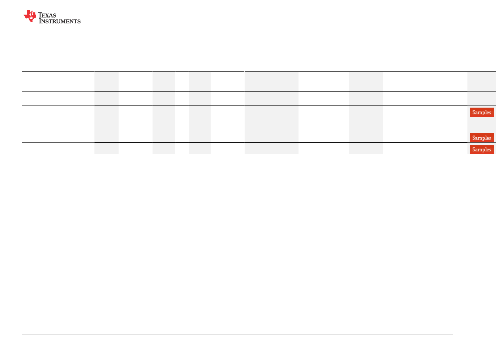
Orderable Device Status
DS90LT012ATMF NRND SOT-23 DBV 5 1000 Non-RoHS
DS90LT012ATMF/NOPB ACTIVE SOT-23 DBV 5 1000 RoHS & Green SN Level-1-260C-UNLIM -40 to 85 N03
DS90LV012ATMF NRND SOT-23 DBV 5 1000 Non-RoHS
DS90LV012ATMF/NOPB ACTIVE SOT-23 DBV 5 1000 RoHS & Green SN Level-1-260C-UNLIM -40 to 85 N02
DS90LV012ATMFX/NOPB ACTIVE SOT-23 DBV 5 3000 RoHS & Green SN Level-1-260C-UNLIM -40 to 85 N02
(1)
The marketing status values are defined as follows:
ACTIVE: Product device recommended for new designs.
LIFEBUY: TI has announced that the device will be discontinued, and a lifetime-buy period is in effect.
NRND: Not recommended for new designs. Device is in production to support existing customers, but TI does not recommend using this part in a new design.
PREVIEW: Device has been announced but is not in production. Samples may or may not be available.
OBSOLETE: TI has discontinued the production of the device.
Package Type Package
(1)
Drawing
Pins Package
Qty
Eco Plan
(2)
& Green
& Green
Lead finish/
Ball material
(6)
Call TI Call TI -40 to 85 N03
Call TI Call TI -40 to 85 N02
MSL Peak Temp
(3)
Op Temp (°C) Device Marking
(4/5)
(2)
RoHS: TI defines "RoHS" to mean semiconductor products that are compliant with the current EU RoHS requirements for all 10 RoHS substances, including the requirement that RoHS substance
do not exceed 0.1% by weight in homogeneous materials. Where designed to be soldered at high temperatures, "RoHS" products are suitable for use in specified lead-free processes. TI may
reference these types of products as "Pb-Free".
RoHS Exempt: TI defines "RoHS Exempt" to mean products that contain lead but are compliant with EU RoHS pursuant to a specific EU RoHS exemption.
Green: TI defines "Green" to mean the content of Chlorine (Cl) and Bromine (Br) based flame retardants meet JS709B low halogen requirements of <=1000ppm threshold. Antimony trioxide based
flame retardants must also meet the <=1000ppm threshold requirement.
(3)
MSL, Peak Temp. - The Moisture Sensitivity Level rating according to the JEDEC industry standard classifications, and peak solder temperature.
(4)
There may be additional marking, which relates to the logo, the lot trace code information, or the environmental category on the device.
(5)
Multiple Device Markings will be inside parentheses. Only one Device Marking contained in parentheses and separated by a "~" will appear on a device. If a line is indented then it is a continuation
of the previous line and the two combined represent the entire Device Marking for that device.
(6)
Lead finish/Ball material - Orderable Devices may have multiple material finish options. Finish options are separated by a vertical ruled line. Lead finish/Ball material values may wrap to two
lines if the finish value exceeds the maximum column width.
Samples
Addendum-Page 1

PACKAGE OPTION ADDENDUM
www.ti.com
Important Information and Disclaimer:The information provided on this page represents TI's knowledge and belief as of the date that it is provided. TI bases its knowledge and belief on information
provided by third parties, and makes no representation or warranty as to the accuracy of such information. Efforts are underway to better integrate information from third parties. TI has taken and
continues to take reasonable steps to provide representative and accurate information but may not have conducted destructive testing or chemical analysis on incoming materials and chemicals.
TI and TI suppliers consider certain information to be proprietary, and thus CAS numbers and other limited information may not be available for release.
27-Apr-2021
In no event shall TI's liability arising out of such information exceed the total purchase price of the TI part(s) at issue in this document sold by TI to Customer on an annual basis.
Addendum-Page 2

PACKAGE MATERIALS INFORMATION
www.ti.com 29-Sep-2019
TAPE AND REEL INFORMATION
*All dimensions are nominal
Device Package
DS90LT012ATMF SOT-23 DBV 5 1000 178.0 8.4 3.2 3.2 1.4 4.0 8.0 Q3
DS90LT012ATMF/NOPB SOT-23 DBV 5 1000 178.0 8.4 3.2 3.2 1.4 4.0 8.0 Q3
DS90LV012ATMF SOT-23 DBV 5 1000 178.0 8.4 3.2 3.2 1.4 4.0 8.0 Q3
DS90LV012ATMF/NOPB SOT-23 DBV 5 1000 178.0 8.4 3.2 3.2 1.4 4.0 8.0 Q3
DS90LV012ATMFX/NOPB SOT-23 DBV 5 3000 178.0 8.4 3.2 3.2 1.4 4.0 8.0 Q3
Type
Package
Drawing
Pins SPQ Reel
Diameter
(mm)
Reel
Width
W1 (mm)
A0
(mm)B0(mm)K0(mm)P1(mm)W(mm)
Pin1
Quadrant
Pack Materials-Page 1

PACKAGE MATERIALS INFORMATION
www.ti.com 29-Sep-2019
*All dimensions are nominal
Device Package Type Package Drawing Pins SPQ Length (mm) Width (mm) Height (mm)
DS90LT012ATMF SOT-23 DBV 5 1000 210.0 185.0 35.0
DS90LT012ATMF/NOPB SOT-23 DBV 5 1000 210.0 185.0 35.0
DS90LV012ATMF SOT-23 DBV 5 1000 210.0 185.0 35.0
DS90LV012ATMF/NOPB SOT-23 DBV 5 1000 210.0 185.0 35.0
DS90LV012ATMFX/NOPB SOT-23 DBV 5 3000 210.0 185.0 35.0
Pack Materials-Page 2

PACKAGE OUTLINE
PIN 1
INDEX AREA
2X 0.95
1.9
0.5
5X
0.3
0.2 C A B
A
3.05
2.75
SOT-23 - 1.45 mm max heightDBV0005A
SMALL OUTLINE TRANSISTOR
C
0.1 C
1.45
0.90
(1.1)
0.15
0.00
TYP
SCALE 4.000
3.0
2.6
1.75
1.45
1
2
3
B
5
1.9
4
0.25
GAGE PLANE
8
TYP
0
0.6
0.3
TYP
SEATING PLANE
0.22
0.08
TYP
4214839/E 09/2019
NOTES:
1. All linear dimensions are in millimeters. Any dimensions in parenthesis are for reference only. Dimensioning and tolerancing
per ASME Y14.5M.
2. This drawing is subject to change without notice.
3. Refernce JEDEC MO-178.
4. Body dimensions do not include mold flash, protrusions, or gate burrs. Mold flash, protrusions, or gate burrs shall not
exceed 0.15 mm per side.
www.ti.com

EXAMPLE BOARD LAYOUT
SOT-23 - 1.45 mm max heightDBV0005A
SMALL OUTLINE TRANSISTOR
2X (0.95)
(R0.05) TYP
SOLDER MASK
OPENING
5X (0.6)
5X (1.1)
PKG
1
2
3
(2.6)
LAND PATTERN EXAMPLE
EXPOSED METAL SHOWN
SCALE:15X
METAL
METAL UNDER
SOLDER MASK
5
SYMM
(1.9)
4
SOLDER MASK
OPENING
EXPOSED METAL
0.07 MAX
ARROUND
NON SOLDER MASK
DEFINED
(PREFERRED)
EXPOSED METAL
0.07 MIN
ARROUND
SOLDER MASK
DEFINED
SOLDER MASK DETAILS
NOTES: (continued)
5. Publication IPC-7351 may have alternate designs.
6. Solder mask tolerances between and around signal pads can vary based on board fabrication site.
4214839/E 09/2019
www.ti.com

5X (0.6)
2X(0.95)
1
2
EXAMPLE STENCIL DESIGN
SOT-23 - 1.45 mm max heightDBV0005A
SMALL OUTLINE TRANSISTOR
PKG
5X (1.1)
5
SYMM
(1.9)
(R0.05) TYP
3
(2.6)
SOLDER PASTE EXAMPLE
BASED ON 0.125 mm THICK STENCIL
SCALE:15X
4
4214839/E 09/2019
NOTES: (continued)
7. Laser cutting apertures with trapezoidal walls and rounded corners may offer better paste release. IPC-7525 may have alternate
design recommendations.
8. Board assembly site may have different recommendations for stencil design.
www.ti.com

IMPORTANT NOTICE AND DISCLAIMER
TI PROVIDES TECHNICAL AND RELIABILITY DATA (INCLUDING DATASHEETS), DESIGN RESOURCES (INCLUDING REFERENCE
DESIGNS), APPLICATION OR OTHER DESIGN ADVICE, WEB TOOLS, SAFETY INFORMATION, AND OTHER RESOURCES “AS IS”
AND WITH ALL FAULTS, AND DISCLAIMS ALL WARRANTIES, EXPRESS AND IMPLIED, INCLUDING WITHOUT LIMITATION ANY
IMPLIED WARRANTIES OF MERCHANTABILITY, FITNESS FOR A PARTICULAR PURPOSE OR NON-INFRINGEMENT OF THIRD
PARTY INTELLECTUAL PROPERTY RIGHTS.
These resources are intended for skilled developers designing with TI products. You are solely responsible for (1) selecting the appropriate
TI products for your application, (2) designing, validating and testing your application, and (3) ensuring your application meets applicable
standards, and any other safety, security, or other requirements. These resources are subject to change without notice. TI grants you
permission to use these resources only for development of an application that uses the TI products described in the resource. Other
reproduction and display of these resources is prohibited. No license is granted to any other TI intellectual property right or to any third party
intellectual property right. TI disclaims responsibility for, and you will fully indemnify TI and its representatives against, any claims, damages,
costs, losses, and liabilities arising out of your use of these resources.
TI’s products are provided subject to TI’s Terms of Sale (https:www.ti.com/legal/termsofsale.html) or other applicable terms available either
on ti.com or provided in conjunction with such TI products. TI’s provision of these resources does not expand or otherwise alter TI’s
applicable warranties or warranty disclaimers for TI products.IMPORTANT NOTICE
Mailing Address: Texas Instruments, Post Office Box 655303, Dallas, Texas 75265
Copyright © 2021, Texas Instruments Incorporated
 Loading...