

Page 1

DS125DF1610EVM
User's Guide
Literature Number: SNLU159B
April 2014–Revised September 2018
Page 2

DS125DF1610EVM
The following user guide details the functionality of DS125DF1610 Evaluation Board Module (EVM) as
well as the Graphic User Interface (GUI) based tool SigCon Architect. The DS125DF1610 device profile
can be used to read and write register settings via the SMBus. For a functional description of the
DS125DF1610, refer to the DS125DF1610 data sheet.
Topic ........................................................................................................................... Page
1 Hardware Overview .............................................................................................. 3
2 Required Software ............................................................................................... 4
3 Setup Instructions................................................................................................ 4
4 Selection Sidebar................................................................................................. 5
5 Configuration Tab ................................................................................................ 5
6 Low Level Tab ..................................................................................................... 6
7 EEPROM Tab....................................................................................................... 6
8 Eye Monitor Tab .................................................................................................. 7
9 Device Status Tab ................................................................................................ 8
10 Transmitter Tab ................................................................................................... 8
11 Receiver Tab ....................................................................................................... 9
12 CDR Tab............................................................................................................ 11
13 PRBS Generator/Checker Tab.............................................................................. 12
14 Cross Point Switch Tab....................................................................................... 12
15 Scripting Tab ..................................................................................................... 13
User's Guide
SNLU159B–April 2014–Revised September 2018
2
DS125DF1610EVM
SNLU159B–April 2014–Revised September 2018
Copyright © 2014–2018, Texas Instruments Incorporated
Submit Documentation Feedback
Page 3
www.ti.com
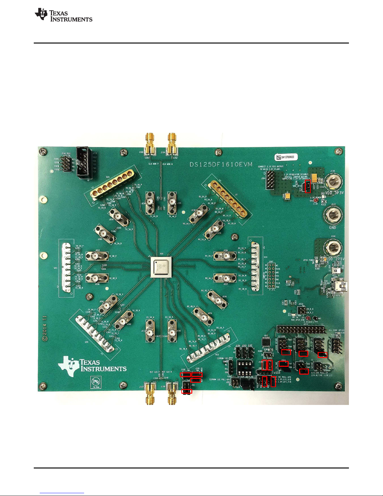
1 Hardware Overview
The DS125DF1610 evaluation board can be powered from a 3.3 V or 2.5 V power supply via banana
cables. There are 4 quads each with 4 channels for a total of 16 channels. Channels 8 – 11 are connected
via SMA connectors. All other channels require MXP connectors that are sold separately and not included
when purchasing the evaluation module. An external reference clock can be applied to speed up the lock
process, but is not required. A 25 MHz, 125 MHz, or 312.5 MHz reference clock can be applied with the 2
former frequencies allowing a single-ended input (312.5 MHz must be differential). Refer to the datasheet
for additional details. The DS125DF1610EVM as shown in Figure 1 is configured with default jumper
settings. For a description of each jumpers function, refer to Table 1 below. Note that the jumper settings
are not in numerical order, but instead are based on their location as you move clockwise around the edge
of the board starting from the banana plugs.
Hardware Overview
SNLU159B–April 2014–Revised September 2018
Submit Documentation Feedback
Figure 1. DS125DF1610Evaluation Board
Copyright © 2014–2018, Texas Instruments Incorporated
DS125DF1610EVM
3
Page 4

Required Software
Table 1. Default Jumper Settings
Jumper Default Setting Description
J207 All pins open MSP430 Microcontroller Connections
J223 All pins open MSP430 Microcontroller Connections
J216 All pins open MSP430 Microcontroller Connections
J183 All pins open All Done GPIO3
J182 Tie Pin 7 – 8 Read EN GPIO2
J191 All pins open Interrupt I/O
J181 Tie Pin 7 – 8 Address Bit1, GPIO1
J192 Tie Pin 1 – 3 Reset I/O
J180 Tie Pin 7 – 8 Address Bit0, GPIO0
J203 Tie Pin 2 – 4 EN SMBus
J222 All pins open TXB0107 Voltage Level Translator Output Enable
J193
J88 All pins open SMBus Access
J215
J162 All pins open EEPROM Address Bit
J163 All pins open EEPROM Address Bit
J164 All pins open EEPROM Address Bit
J82 All pins open EEPROM Write Protect Bit
J175 All pins open EEPROM SMBus
J202 All pins open EEPROM SMBus
J206 All pins open EEPROM SMBus Pull-Ups
J108
J109 Tie Pin 1 – 3 Oscillator Output Enable
J99 Tie Pin 2 – 4 Oscillator Frequency Select
J179 All pins open DS125DF1610 Retimer Connections
JP13 All pins open DS125DF1610 Retimer Connections
J204 All pins open 2.5 V and LDO Power Plane Connection
J198 Tie Pin 1 – 2 LDO Enable Pull-Up
Tie pin 1 -2
Tie pin 3 -4
Tie Pin 3 – 4
Tie Pin 7 – 8
Tie Pin 1 – 3
Tie Pin 2 – 4
MSP430 Microcontroller Connections
Pull-Ups for SMBus
Oscillator Power
www.ti.com
2 Required Software
• SigCon Architect
• DS125DF1610 Profile for SigCon Architect
3 Setup Instructions
• Navigate to the DS125DF1610EVM product page on TI.com.
• Follow the guide at SNLU178 to install the SigCon Architect software, and for ease of use, add the
shortcut to the desktop. With the software still closed, run the device profile updater for the
DS125DF1610 as indicated in the previous guide.
• Hook up the power supply to the DS125DF1610EVM with the output disabled.
• Using the USB2ANY, the USB cable can be connected directly to the USB port on the EVM board and
the computer.
• Click the shortcut to open the SigCon Architect software. If prompted to run as administrator, select
yes.
4
DS125DF1610EVM
SNLU159B–April 2014–Revised September 2018
Copyright © 2014–2018, Texas Instruments Incorporated
Submit Documentation Feedback
Page 5
www.ti.com
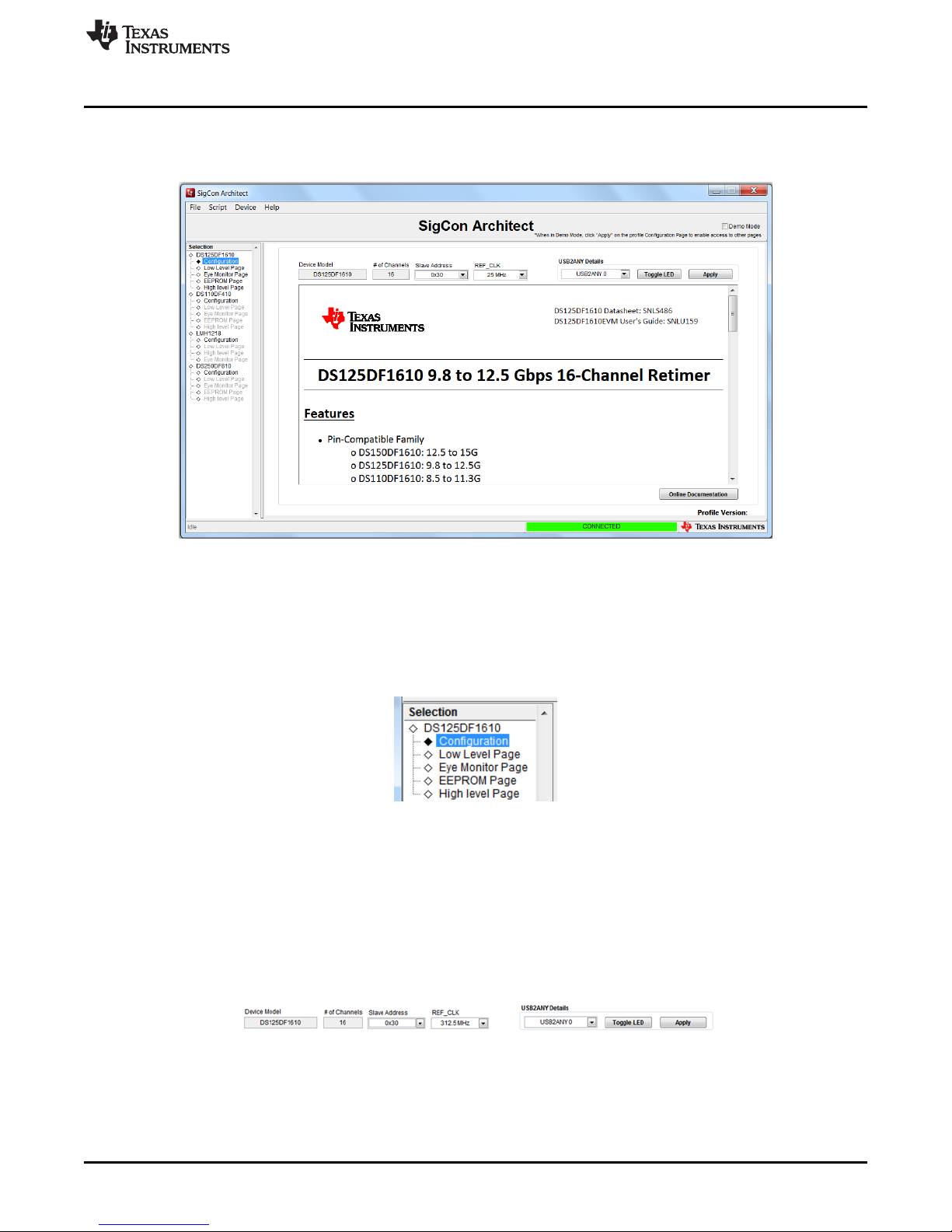
When starting SigCon architect, the graphic user interface should appear as in Figure 2 with the
DS150DF1610 Retimer profile already loaded. In order to initiate reading and writing of the registers, the
‘Demo Mode’ box in the upper right hand corner must be deselected.
Selection Sidebar
4 Selection Sidebar
The ‘selection’ sidebar shows the current active device profiles. When the device is active and
configurable, this will show the sub-pages that are used to control the device: Configuration, Low Level
Page, Eye Monitor Page, EEPROM Page, and High Level Page.
The content on each of these sub-pages will be detailed in each of the following sections.
5 Configuration Tab
The configuration tab’s main purpose is to specify the slave address for successful communication with
the DS125DF1610EVM. The default address is hex 0x30 as shown in Figure 4. If the ADDR0 (GPIO0) or
ADDR1 (GPIO1) jumper settings are altered, the SMBus address will need to be changed. Refer to the
datasheet for additional information.
Figure 2. DS125DF1610 Profile GUI
Figure 3. Selection Sidebar
After selecting the proper slave address, the board can be connected by clicking the apply button. If the
USB2ANY details drop down box does not show any values, then the board is not correctly connected to
your computer.
SNLU159B–April 2014–Revised September 2018
Submit Documentation Feedback
Figure 4. Configuration Tab
Copyright © 2014–2018, Texas Instruments Incorporated
DS125DF1610EVM
5
Page 6
Low Level Tab
Make sure to set the REF_CLK value to the 312.5 MHz value, as this is the default for this board.
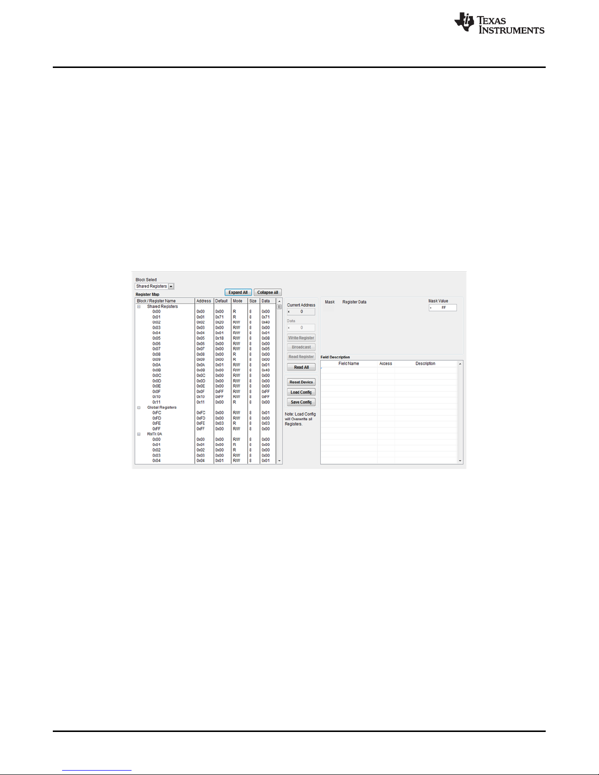
6 Low Level Tab
In this tab, the user can find all of the register values that are on the DS125DF1610 board, including both
shared values and values unique to each of the input and output channels.
The Expand / Collapse all buttons can be used to show and hide all of the registers on the list. In order to
read the most recent settings from the board, use the Read All button to update the state of each of the
registers. In order to update only one of the registers, use the Read Register.
In order to adjust all of the registers in bulk, 4 additional buttons are available. The load config and save
config buttons will load and save the contents of all registers on the board. These .cfg files store all
registers in order with data in hexadecimal. The file can be edited in your favorite text editor. A simple way
to restore custom settings is to load your saved config files. The reset device button will reset the registers
and the board to their original configuration.
The fourth button is the broadcast button, which the user can utilize when it is necessary to change a
channel register on each of the 16 channels simultaneously.
www.ti.com
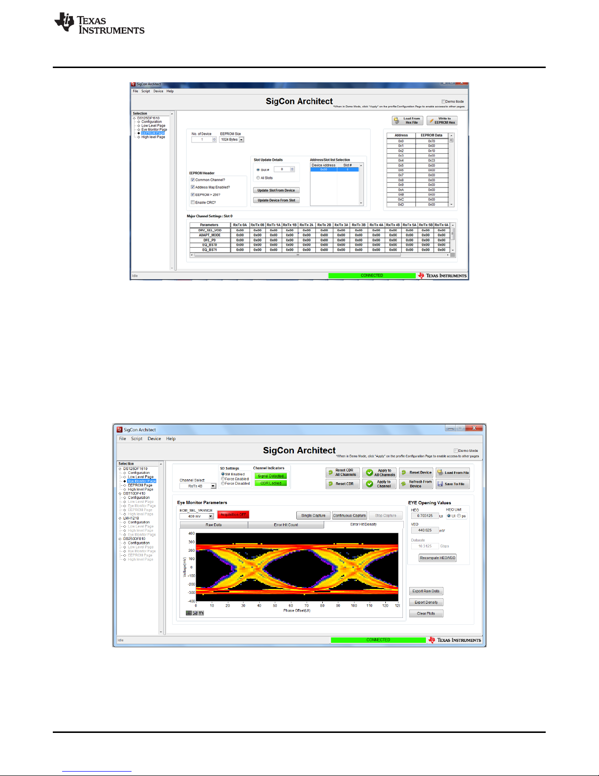
7 EEPROM Tab
If the desired shared register settings are stored in EEPROM the ‘Device from Slot’ push button should be
selected in order to write to the retimer registers. To write the current shared register settings in the GUI to
EEPROM, the ‘Slot from Device’ push button should be selected.
Saving and loading the EEPROM configuration hex file can be performed with the Load from Hex File, and
Write to EEPROM Hex buttons.
6
DS125DF1610EVM
Figure 5. Low Level Tab
SNLU159B–April 2014–Revised September 2018
Copyright © 2014–2018, Texas Instruments Incorporated
Submit Documentation Feedback
Page 7
www.ti.com
8 Eye Monitor Tab
The internal eye monitor functionality can be controlled by the Eye Monitor Tab as shown in Figure 7.
Under the Channel Indicators (in Red) the CDR must be locked and a signal detected before the eye
monitor can be turned on. Prior to turning on the Eye Monitor, the Eye Monitor Voltage must be selected,
as well as the Channel Selected (Blue). The eye monitor plot must then be turned on with either the single
capture or continuous capture modes. A device reset is also included in this tab. After acquiring the data
from the eye monitor, the horizontal and vertical eye openings, HEO and VEO, can be viewed under EYE
opening values.
Eye Monitor Tab
Figure 6. EEPROM Tab
SNLU159B–April 2014–Revised September 2018
Submit Documentation Feedback
Figure 7. Internal Eye Monitor Tab
Copyright © 2014–2018, Texas Instruments Incorporated
DS125DF1610EVM
7
Page 8

Device Status Tab
On the bottom right hand side of the monitor are the three buttons used to manipulate the data within the
monitor. The export raw data button allows the user to export this collected data as an excel spreadsheet
with values to interpret the darkness of the eye monitor. The export density button allows the user to
export the collected density values from the eye monitor plot, again as an excel spreadsheet with the
values of density as the cell values. The clear plots button allows the user to clear the eye monitor before
capturing the next set of data.
9 Device Status Tab
This tab gives a brief summary of the status on all of the channels in the device. This includes whether
there is a signal or a lock on each channel, as well as a summary of the CTLE, DFE, EOM, and transmit
settings for the channel.
www.ti.com
10 Transmitter Tab
The transmitter tab controls the various level settings for VOD, the 3 taps of the FIR filter, and in addition
has indicators for when a signal is detected as well as when the CDR locks for all 16 transmitter channels
as shown in Figure 9.
The ‘Channel Select’ pull down menu is used to select which of the 16 channels is being modified. For the
Channel Indicators box, when a signal is detected the ‘Signal Detect’ indicator will switch from being red
and reading No Signal to green and should read Signal Detected. If the CDR locks to the applied data
rate, the indicator should switch to green and read CDR Locked. The ‘Reset’ push button is used to reset
the default transmitter settings. By default the ‘SM Enabled’ icon should be selected to enable the state
machine. In order to force the channel in question to be active as opposed to relying on signal detect,
‘Force Enabled’ can be selected. Conversely, in order to disable a channel regardless of whether a signal
is detected ‘Force Disabled’ can be selected.
Figure 8. Device Status Tab
8
DS125DF1610EVM
SNLU159B–April 2014–Revised September 2018
Copyright © 2014–2018, Texas Instruments Incorporated
Submit Documentation Feedback
Page 9

www.ti.com
The DS125DF1610 output driver has 22 VOD level settings ranging from 150 mV to 1200 mV in 50 mV
increments. When the retimer is reset, the VOD level will return to the default value of 1000 mV. The
‘Edge Rate Select’ option allows the user to adjust the rise and fall time for the output signal, with the
default setting being the fastest rise/fall time.
The ‘Transmit FIR Control’ section consists of 3 FIR taps; pre-cursor, main-cursor, and post-cursor. The
pre-cursor and post-cursor taps emphasize the output voltage level to account for high frequency losses.
The main cursor primarily is used to balance the other two taps in order to sum to the appropriate
normalized sum value which based on the selected VOD setting. The pre-cursor, main cursor, and postcursor taps of the FIR filter are each adjusted on a scale of 0 – 63 but should be normalized based on the
selected VOD setting. Normalizing the taps can be performed either by selecting the Normalize before
applying checkbox, or by clicking the normalize taps button.
However, each of the 3 taps can be set to any of the 64 levels without being normalized. This is not
recommended as a starting point, but is a feature that can be utilized. To write the tap settings to the
register without normalizing them, ‘Normalize Before Applying’ must be deselected.
The ‘Normalize Taps’ push button will adjust the main cursor in order to sum the 3 taps to the value
predefined by the VOD setting the user selects. However, if the ‘Normalize Before Applying’ checkbox is
selected the 3 taps will be normalized when writing them to the register. The ‘Read Taps’ push button will
populate the current register settings for the pre, post, and main cursor taps into the corresponding fields.
‘Set Taps’ will write the pre, main, and post cursor settings into the register.
Receiver Tab
Figure 9. Transmitter Tab
11 Receiver Tab
The Receiver tab controls all the relevant functionality associated with the 16 receiver channels of the
DS125DF1610EVM. The ‘Signal Detect’ and ‘CDR Lock’ indicators are identical to the Transmitter Tab,
reflecting when a signal is detected or when the CDR locks. ‘Channel Select,’ ‘Update Time,’ and ‘Reset’
are all similar to the Transmitter Tab.
SNLU159B–April 2014–Revised September 2018
Submit Documentation Feedback
Copyright © 2014–2018, Texas Instruments Incorporated
DS125DF1610EVM
9
Page 10

Receiver Tab
The ‘Adapt Mode Selection’ section is for the setting the adapt mode of the DS125DF1610. Refer to
Table 2 for explanations of each adapt mode.
www.ti.com
Figure 10. Receiver Tab
Table 2. Adapt Mode Descriptions
Adapt Mode Description
0 Manual Setting of CTLE and DFE, no adaptation
1 Adapt CTLE only
2 Adapt CTLE until optimal, then DFE, then CTLE again
3 Adapt CTLE until lock, then DFE, then CTLE until optimal
The EQ boost settings are divided into 4 stages, each with 2-bit boost control for a total of 256 different
stage-boost combinations. In order to select the EQ boost settings, the device must be in Adapt Mode 0.
In the other Adapt modes the CTLE will adapt through 32 of these stage-boost combinations. The CTLE
adaptation can be set to limiting mode by selecting the ‘Boost 3: Limiting Bit’ check box. The ‘Load CTLE
Table’ push button is used to specify the 32 EQ settings that the CTLE should cycle through.
The ‘DFE Control’ area of the Receiver Tab is used for setting the 5 taps of the DFE. Tap 1 has 32
settings from 0 to 224 mV in 7 mV increments. See Table 3 for details. These values should be entered in
hex from 0x00 to 0x1F. Taps 2 through 5 have 16 settings each from 0 to 112 mV in 7 mV increments and
should be entered in hex from 0x00 to 0x0F. The polarity of each tap can also be adjusted, with a
negative polarity representing boost and positive representing an attenuation of the data. In order to set
the DFE Taps manually (only Adapt Mode 0), ‘Enable Manual Tap Control’ must be selected and ‘DFE
Enable’ must also be turned on. ‘Clear Taps’ will reset all of the tap values to 0mV (0x00). When in an
adapt mode where the DFE will adapt automatically, it can be configured to adapt only during lock
acquisition or to adapt continuously with the “Continuous DFE Adaptation” checkbox.
Table 3. DFE Tap Parameters
DFE Parameter Value (mV)
Tap 1 Weight Range 0 - 224
Tap 2-5 Weight Range 0 - 112
Tap Weight Step Size 7
10
DS125DF1610EVM
SNLU159B–April 2014–Revised September 2018
Copyright © 2014–2018, Texas Instruments Incorporated
Submit Documentation Feedback
Page 11

www.ti.com
12 CDR Tab
Within the ‘Mode Selection’ section there are two options for setting the data rate that the DS125DF1610
expects to receive – ‘Standard Rate’ and ‘Manual Mode.’ ‘Standard rate’ gives the user the option to select
the data rate they are running at for a defined set of protocols, without having to manually program the
expected data rate. See Table 4 for additional details.
CDR Tab
Table 4. Standard Mode Data Rates
Channel Register
0x2F[7:4] Setting
0x6 Custom 11.5 1 1
0x7 Interlaken 12.5, 6.25, 3.125 1, 2, 4 1, 2, 4
0x8 CPRI 1 9.8304, 4.9152, 2.4576 1, 2, 4 1, 2, 4
0x9 CPRI 2 6.144, 3.072 2, 4 2, 4
0xA Infiniband 10, 5, 2.5 1, 2, 4 1, 2, 4
0xB Ethernet 10.3125, 1.25 8 1
Standard Data Rates (Gbps) First Group Divider Settings
Second Group Divider
Settings
The alternative to ‘Standard Rate’ mode is to program the expected data rate in ‘Manual Mode.’ In manual
mode the desired data rate and corresponding VCO frequency must be entered into Group One or Group
Two. Refer to the datasheet Register Map for setting the 0x2F [7:4] register bits. The bits should be set
based on the expected date rate, taking into account which divider will be required. For example if a data
rate of 1.25 Gbps is entered into the desired VCO frequency for Group One, 0x0C should be selected due
to it having an 8 divider since 1.25 Gbps is a division of 10.3125 Gbps by 8. When a date rate is manually
entered into the ‘Desired VCO Frequency’ field the ‘Write Rate Reg’ push button must be selected to write
it to the register. The desired ppm tolerance is used to adjust the lock range of the CDR for the receiver
channel in question. The VCO count and PPM delta count fields are automatically populated based on the
specified data rate.
SNLU159B–April 2014–Revised September 2018
Submit Documentation Feedback
Figure 11. CDR Tab
Copyright © 2014–2018, Texas Instruments Incorporated
DS125DF1610EVM
11
Page 12

PRBS Generator/Checker Tab
13 PRBS Generator/Checker Tab
The DS125DF1610 is equipped with an on-board PRBS generator as well as a PRBS checker. The PRBS
generator and PRBS checker should be operated from different channels. The PRBS generator can
generate a pseudo-random bit sequence on the transmit side of a channel. It can then be run through a
cable or backplane, and checked by the receiver channel that is configured for the PRBS checker. The
PRBS Checker must be enabled in the ‘PRBS Checker Enable/Disable Selection’ section. In order to reset
the PRBS sequence, the ‘Reset PRBS’ push button can be selected. In the ‘PRBS Pattern Status’ section
the checker will read the PRBS pattern whether that be PRBS31, PRBS15, PRBS9, or PRBS7. It will
populate the inverted or non-inverted field, as well as provide the error count, bit count, and the error rate.
The ‘PRBS Generator’ section is where the PRBS sequence length can be set. However instead of
generating a PRBS sequence, an 8-bit user pattern can be created and also inverted if desired.
www.ti.com
14 Cross Point Switch Tab
In this tab the cross point functionality of the DS125DF1610EVM can be configured. It is divided up into 4
quads or switch matrices, each with 4 channels. By default, the DS125DF1610EVM has no cross-point
enabled and the receiver channel will route to the same transmit channel. The cross point functionality can
be used to create point to point links, or operate in broadcast mode. In point to point switching, one input
channel will be routed to only one output channel. When using broadcast mode, one input can be routed
to two, three, or four output channels. Refer to the DS125DF1610 datasheet for additional information.
The ‘TX CH x Select’ section controls the associations between receive channel and transmit channel.
When setting up point to point switching, the ‘Broadcast Channel section is not used. The ‘Signal Detected
and CDR locked’ will indicate when a receiver channel is detecting a signal, as well as indicate when the
CDR locks for a selected transmit channel. When operating the broadcast function, a master must be
selected in order to dictate which output channel will send back its adapt data to the CTLE. Refer to the
datasheet for additional information. Only one master transmit (output) channel should be selected, as
there cannot be more than one master channel in a broadcast network.
Figure 12. PRBS Generator/Checker Tab
12
DS125DF1610EVM
SNLU159B–April 2014–Revised September 2018
Copyright © 2014–2018, Texas Instruments Incorporated
Submit Documentation Feedback
Page 13

www.ti.com
Scripting Tab
Figure 13. Cross Point Switch Control Tab
15 Scripting Tab
The scripting tab is a Python-based script for coding channel and shared register settings. To access the
scripting function click the Script button on the upper menu bar. Click launch window and start recording to
save a process of configuration into a Python script. After finished, select stop recording from the same
menu.
SNLU159B–April 2014–Revised September 2018
Submit Documentation Feedback
Figure 14. Scripting Tab
Copyright © 2014–2018, Texas Instruments Incorporated
DS125DF1610EVM
13
Page 14

Revision History
www.ti.com
Revision History
NOTE: Page numbers for previous revisions may differ from page numbers in the current version.
Changes from A Revision (January 2017) to B Revision ............................................................................................... Page
• Changed J193 all pins open to tie 1-2 and 3-4........................................................................................ 4
Changes from Original (April 2014) to A Revision .......................................................................................................... Page
• Changed picture in Figure 1 ............................................................................................................. 3
• Changed sections 2-15 from supporting Analog Launch Pad to Sigcon Architect ............................................... 4
14
Revision History
SNLU159B–April 2014–Revised September 2018
Copyright © 2014–2018, Texas Instruments Incorporated
Submit Documentation Feedback
Page 15

IMPORTANT NOTICE AND DISCLAIMER
TI PROVIDES TECHNICAL AND RELIABILITY DATA (INCLUDING DATASHEETS), DESIGN RESOURCES (INCLUDING REFERENCE
DESIGNS), APPLICATION OR OTHER DESIGN ADVICE, WEB TOOLS, SAFETY INFORMATION, AND OTHER RESOURCES “AS IS”
AND WITH ALL FAULTS, AND DISCLAIMS ALL WARRANTIES, EXPRESS AND IMPLIED, INCLUDING WITHOUT LIMITATION ANY
IMPLIED WARRANTIES OF MERCHANTABILITY, FITNESS FOR A PARTICULAR PURPOSE OR NON-INFRINGEMENT OF THIRD
PARTY INTELLECTUAL PROPERTY RIGHTS.
These resources are intended for skilled developers designing with TI products. You are solely responsible for (1) selecting the appropriate
TI products for your application, (2) designing, validating and testing your application, and (3) ensuring your application meets applicable
standards, and any other safety, security, or other requirements. These resources are subject to change without notice. TI grants you
permission to use these resources only for development of an application that uses the TI products described in the resource. Other
reproduction and display of these resources is prohibited. No license is granted to any other TI intellectual property right or to any third
party intellectual property right. TI disclaims responsibility for, and you will fully indemnify TI and its representatives against, any claims,
damages, costs, losses, and liabilities arising out of your use of these resources.
TI’s products are provided subject to TI’s Terms of Sale (www.ti.com/legal/termsofsale.html) or other applicable terms available either on
ti.com or provided in conjunction with such TI products. TI’s provision of these resources does not expand or otherwise alter TI’s applicable
warranties or warranty disclaimers for TI products.
Mailing Address: Texas Instruments, Post Office Box 655303, Dallas, Texas 75265
Copyright © 2018, Texas Instruments Incorporated
 Loading...