

Page 1

DS125BR800EVM User’s Guide
User's Guide
Literature Number: SNLU122
November 2012
Page 2

User's Guide
SNLU122–November 2012
DS125BR800EVM Evaluation Kit
The DS125BR800EVM – SMA evaluation kit provides a complete high band-width platform to evaluate the
signal integrity and signal conditioning features of the Texas Instruments signal conditioning products –
with Equalization and De-emphasis. SMA edge launch connectors are used as the input and the output
connections for this evaluation board. Commercially available adaptor boards can be purchased to
facilitate connection to cables or backplane interconnects.
Topic ........................................................................................................................... Page
1 Features ............................................................................................................. 3
2 4-Level IO Control ............................................................................................... 5
3 Switch Connection Overview ................................................................................ 6
4 Quick Start Guide ................................................................................................ 7
5 SMBus Slave Mode of the EQ, VOD, and De-Emphasis level: .................................. 10
6 Bill of Materials for DS125BR800EVM: ................................................................. 11
7 Schematic for DS125BR800EVM: ......................................................................... 12
8 EVM Layout ...................................................................................................... 13
2
DS125BR800EVM Evaluation Kit SNLU122–November 2012
Copyright © 2012, Texas Instruments Incorporated
Submit Documentation Feedback
Page 3
www.ti.com
1 Features
• 8 Channel Repeater up to 12.5 Gbps
• Low 65 mW/channel power consumption, with option to power down unused channels
• Transparent management of link training protocol for PCIe, SAS, and 10G-KR
• Receive Equalization up to 30 dB at 12.5 Gbps
• Settable transmit de-emphasis driver to -12 dB
• Transmit output voltage control: 700 – 1300 mV
• Programmable via pin selection, EEPROM, or SMBus interface
• Single supply operation: VIN = 3.3V±10% or VDD = 2.5V ±5%
• -40°C to +85°C Operation
• 5 kV HBM ESD rating
• High speed signal flow–thru pin-out package: 54-pin QFN (10 mm x 5.5 mm, 0.5 mm pitch)
Applications
FR-4 Backplane Traces and High Speed Cable
Ordering Information
EVM ID DEVICE ID DEVICE PACKAGE
DS125BR800EVM DS125BR800SQE/NOPB QFN-54
Features
SNLU122–November 2012 DS125BR800EVM Evaluation Kit
Submit Documentation Feedback
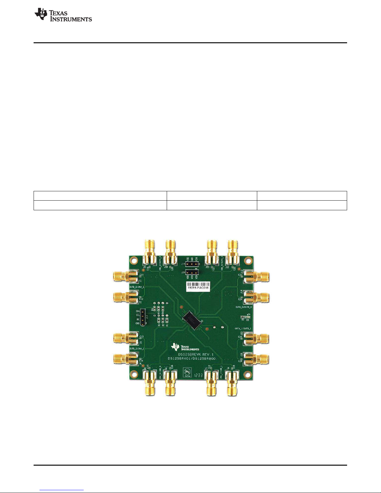
Figure 1. DS125BREVK REV. 1
DS125BR401/DS125BR800 Top Assembly
3
Copyright © 2012, Texas Instruments Incorporated
Page 4

Features
www.ti.com
Figure 2. DS125BREVK REV. 1
DS125BR401/DS125BR800 Bottom Assembly
4
DS125BR800EVM Evaluation Kit SNLU122–November 2012
Copyright © 2012, Texas Instruments Incorporated
Submit Documentation Feedback
Page 5
www.ti.com
2 4-Level IO Control
Many of the control pins on the DS125BR800 have more than two valid levels. Table 1 below shows how
to access each of these levels with the switch banks on the back side of the EVM.
4-Level Input Settings Setting for 3 pin switches (3-2-1)
0 - Tie 1kΩ to GND ON - OFF - OFF
R - Tie 20kΩ to GND OFF - ON - OFF
F - FLOAT (open) OFF - OFF - OFF
1 - Tie 1kΩ to VIH OFF - OFF - ON
The following switches are used to set the input condition for the 4-level inputs:
• SW1, SW2, SW3, SW5, SW6, SW8, SW9
There are 3 switches connected to an input signal pin. Each switch when set to the ON position sets the
pin to one of the 4-level setting. The 6 pin switches are assigned similar to the 3 pin switches. The only
difference is 2 signal pins are connected and thus 6-5-4 is for the one signal pin and 3-2-1 is for another
signal pin.
NOTE: Only 1 switch at the ON position is allowed. Activating more than one switch concurrently
results in an indeterminate voltage level.
4-Level IO Control
Table 1. Switches to set the 4-Level input control pins
SNLU122–November 2012 DS125BR800EVM Evaluation Kit
Submit Documentation Feedback
5
Copyright © 2012, Texas Instruments Incorporated
Page 6

Switch Connection Overview
3 Switch Connection Overview
Table 2. Connection and Control Description
Component Name Function
IN_B2+, IN_B2-,
J1 to J8 High-speed differential inputs
J9 to J16 High-speed differential outputs
J19 VIN or VDD DC Power - VIN or VDD to DS125BR800SQ
J20 VIN or VDD Jumper – VIN or VDD to VIH power
J17 SDA, SCL
J18 EEPROM Optional socket for EEPROM
SW1
SW2 ENSMB
SW3 DEMA[1:0] PIN MODE – DE control for channel A outputs
SW4 SDA/SCL “ON” position connects SDA and SCL lines to the device pin.
SW5
SW6 SD_TH and LPBK - RES
SW7
SW8 EQA[1:0] PIN MODE – EQ control for channel A inputs
SW9 Float = Auto Mode Select (for PCIe and SAS-3)
SW10 READ_EN
IN_B3+, IN_B3-,
IN_A0+, IN_A0-,
IN_A1+, IN_A1-,
OUT_B2+, OUT_B2-,
OUT_B3+, OUT_B3-,
OUT_A0+, OUT_A0-,
OUT_A1+, OUT_A1-,
EQB[1:0] or PIN MODE – EQ control for channel B inputs
AD[3:2] SMBUS MODE – AD[3:2] device address bits
DEMB[1:0] or PIN MODE – DE control for channel B outputs
AD[1:0] SMBUS MODE – AD[1:0] device address bits
VDD_SEL and VDD_SEL – Enable or disable the internal 3.3V to 2.5V regulator.
RESET RESET – Enable or disable the device (LOW – enable)
INPUT_EN and
MODE
www.ti.com
Optional SMBUS access pins.
See the datasheet for additional information on SMBUS.
ENSMB = LOW – PIN MODE
ENSMB = HIGH – SMBUS (slave mode)
ENSMB = FLOAT – SMBUS (master mode – load configuration from
EEPROM)
SD_TH – Signal detect threshold level (FLOAT = Default level)
LPBK function for BR401 only (FLOAT = Normal operation)
INPUT_EN – Enable or disable the internal 50 ohm to VDD terminations
MODE – Tie 1kΩ to GND = GEN 1,2 and SAS 1,2
Tie 20kΩ to GND = SAS-3 and GEN-3 without De-emphasis
Tie 1kΩ to VDD = SAS-3 and GEN-3 with De-emphasis
ENSMB = FLOAT – SMBUS (master mode – load configuration from
EEPROM)
SW6: SD_TH becomes the READ_EN pin.
To start the loading at power up, set SW6 pin 3 to “ON” position (pull to
GND).
To manually control the start, set SW6 pin 1 to “ON” position (pull to VDD)
and push the SW10 button for the high to low transition to start the loading.
When the loading is complete the LED – D1 light should turn OFF.
6
DS125BR800EVM Evaluation Kit SNLU122–November 2012
Copyright © 2012, Texas Instruments Incorporated
Submit Documentation Feedback
Page 7

www.ti.com
4 Quick Start Guide
1. Connect J19: VIN = 3.3V or VDD = 2.5V and GND.
• For VIN = 3.3V:
Set SW7 pin1 (VDD_SEL) to the ON position (enable internal LDO regulator) and float VDD at J19.
• For VIN = 2.5V:
Set SW7 pin1 (VDD_SEL) to the OFF positions (disable internal LDO regulator) and float VIN at
J19.
2. Set jumper – J20 for VIH connection to VIN or VDD.
3. Connect 50 Ohm SMA cables to the board.
• The input signals J1 to J8 can be connected from a pattern generator.Set SW7 pin1 (VDD_SEL) to
the ON position (enable internal LDO regulator) and float VDD at J19.
• The output signals J9 to J16 can be connected to a scope.
A/B Channels Input Channel Output Channel
B-Channels
A-Channels
4. Set the control pins for normal operation
• SW7 – RESET = 0 (enables the device): set switch pin2 to the ON position.
• SW9 – INPUT_EN = 1 (50 ohm input termination): set switches (3-2-1) = (OFF-OFF-ON).
• SW9 – MODE = VDD (enables SAS-3 / PCIe GEN3 mode): set switches (6-5-4) = (OFF-OFF-ON).
• SW6 – SD_TH = F (default signal detect threshold level): set switches (3-2-1) = (OFF-OFF-OFF).
• SW6 – LPBK - RES = F (normal operation): set switches (6-5-4) = (OFF-OFF-OFF).
Quick Start Guide
Table 3. SMA Channel Connections
J1 – IN_B2+, J2 – IN_B2- J9 – OUT_B2+, J10 – OUT_B2J3 – IN_B3+, J4 – IN_B3- J11 – OUT_B3+, J12 – OUT_B3J5 – IN_A0+, J6 – IN_A0- J13 – OUT_A0+, J14 – OUT_A0J7 – IN_A1+, J8 – IN_A1- J15 – OUT_A1+, J16 – OUT_A1-
SNLU122–November 2012 DS125BR800EVM Evaluation Kit
Submit Documentation Feedback
7
Copyright © 2012, Texas Instruments Incorporated
Page 8

Quick Start Guide
5. Set the input equalization level.
• For external pin mode control of the equalization level:
• Set ENSMB = 0 (1kΩ to GND) by using the SW2 (3-2-1) = (ON-OFF-OFF).
• SW4 pin1,2 must be set to the OFF positions, so the SMBUS signals are disconnected.
• Refer to Table 1 for information on the 3 switch settings for the 4 level input.
Example:
• Set EQB[1:0] with SW1 for the B bank of inputs (top 4 inputs of DS125BR800).
• SW1 (6-5-4), (3-2-1) = (OFF-ON-OFF), (OFF-ON-OFF) = EQB[1:0] = R,R (Level 6).
• Set EQA[1:0] with SW8 for the A bank of inputs (bottom 4 inputs of DS125BR800).
• SW8 (6-5-4), (3-2-1) = (OFF-ON-OFF), (OFF-ON-OFF) = EQA[1:0] = R,R (Level 6).
Level EQA/B[1:0] SW1 - EQB[1:0] or SW8 - EQA[1:0] EQ (dB) @ 6 GHz
1 0, 0 ON OFF OFF ON OFF OFF 3.1
2 0, R ON OFF OFF OFF ON OFF 6.7
3 0, F ON OFF OFF OFF OFF OFF 8.4
4 0, 1 ON OFF OFF OFF OFF ON 9.1
5 R, 0 OFF ON OFF ON OFF OFF 13.7
6 R, R OFF ON OFF OFF ON OFF 16.2
7 R, F OFF ON OFF OFF OFF OFF 15.9
8 R, 1 OFF ON OFF OFF OFF ON 17.0
9 F, 0 OFF OFF OFF ON OFF OFF 20.7
10 F, R OFF OFF OFF OFF ON OFF 21.8
11 F, F OFF OFF OFF OFF OFF OFF 23.6
12 F, 1 OFF OFF OFF OFF OFF ON 24.7
13 1, 0 OFF OFF ON ON OFF OFF 28.0
14 1, R OFF OFF ON OFF ON OFF 29.2
15 1, F OFF OFF ON OFF OFF OFF 30.9
16 1, 1 OFF OFF ON OFF OFF ON 31.9
www.ti.com
Table 4. EQ Settings available with PIN MODE
6 5 4 3 2 1
8
DS125BR800EVM Evaluation Kit SNLU122–November 2012
Copyright © 2012, Texas Instruments Incorporated
Submit Documentation Feedback
Page 9

www.ti.com
6. Set the output VOD and De-emphasis level.
Quick Start Guide
• For external pin mode control for the VOD and De-emphasis level:
• Set ENSMB = 0 (1kΩ to GND) by using the SW2 (3-2-1) = (ON-OFF-OFF).
• SW4 pin1,2 must be set to the OFF positions, so the SMBUS signals are disconnected.
• Refer to Table 1 for information on the 3 switch settings for the 4 level input.
Example:
• Set DEMB[1:0] with SW5 for the B bank of outputs (top 4 outputs of DS125BR800).
• SW5 (6-5-4), (3-2-1) = (ON-OFF-OFF), (OFF-OFF-ON) = DEMB[1:0] = 0,1 (VOD=1.0V, DE=0 dB).
• Set DEMA[1:0] with SW3 for the A bank of outputs (bottom 4 outputs of DS125BR800).
• SW3 (6-5-4), (3-2-1) = (ON-OFF-OFF), (OFF-OFF-ON) = DEMA1:0] = 0,1 (VOD=1.0V, DE=0 dB).
Table 5. DE and VOD Settings available in PIN MODE
Level EQA/B[1:0] SW1 - EQB[1:0] or SW8 - EQA[1:0] GEN1 and GEN2
6 5 4 3 2 1 DE (dB)
1 0, 0 ON OFF OFF ON OFF OFF 0.8 0
2 0, R ON OFF OFF OFF ON OFF 0.9 0
3 0, F ON OFF OFF OFF OFF OFF 0.6 -3.5
4 0, 1 ON OFF OFF OFF OFF ON 1.0 0
5 R, 0 OFF ON OFF ON OFF OFF 0.7 -3.5
6 R, R OFF ON OFF OFF ON OFF 0.5 -6
7 R, F OFF ON OFF OFF OFF OFF 1.1 0
8 R, 1 OFF ON OFF OFF OFF ON 0.7 -3.5
9 F, 0 OFF OFF OFF ON OFF OFF 0.6 -6
10 F, R OFF OFF OFF OFF ON OFF 1.2 0
11 F, F OFF OFF OFF OFF OFF OFF 0.8 -3.5
12 F, 1 OFF OFF OFF OFF OFF ON 0.6 -6
13 1, 0 OFF OFF ON ON OFF OFF 1.3 0
14 1, R OFF OFF ON OFF ON OFF 0.9 -3.5
15 1, F OFF OFF ON OFF OFF OFF 0.7 -6
16 1, 1 OFF OFF ON OFF OFF ON 0.5 -9
Inner Amplitude
(VPP)
NOTE: The De-Emphasis levels are also available in SAS-3 / GEN-3 mode when MODE = 1
SNLU122–November 2012 DS125BR800EVM Evaluation Kit
Submit Documentation Feedback
9
Copyright © 2012, Texas Instruments Incorporated
Page 10

SMBus Slave Mode of the EQ, VOD, and De-Emphasis level:
5 SMBus Slave Mode of the EQ, VOD, and De-Emphasis level:
• Set ENSMB = 1 (1kΩ to VIH) by using the SW2 (3-2-1) = (OFF-OFF-ON).
• Set SW4 pin1,2 to the ON position so the SMBUS signals are connected.
• Set SW3 pin1 thru pin6 switches to the OFF position so they do not connect to the SDA and SCL line.
• Set the SW1 and SW5 for the AD[3:0] pins. AD[3:0]=0000 sets device slave address = B0’hex.
• Connect SDA, SCL and GND to J17. Please refer to datasheet for register map for EQ, VOD and
DEM.
www.ti.com
10
DS125BR800EVM Evaluation Kit SNLU122–November 2012
Copyright © 2012, Texas Instruments Incorporated
Submit Documentation Feedback
Page 11

www.ti.com
6 Bill of Materials for DS125BR800EVM:
Table 6. DS125BR800EVM BOM
Item Qty Reference Digikey PN Manufacture PN Descriptions
1 1 C1 445-3448-1-ND C1608Y5V0J106Z CAP CER 10UF 6.3V Y5V 0603
2 1 C2 445-1322-1-ND C1608X5R0J105K CAP CER 1.0UF 6.3V X5R 0603
3 5 445-4711-1-ND C0603X5R0J104M CAP CER .10UF 6.3V X5R 0201
4 16 587-2483-1-ND LMK063BJ224MP-F CAP CER .22UF 10V X5R 0201
5 1 D1 511-1592-1-ND SML-P12PTT86 LED GRN 0.2MM 13MCD 0402 SMD
6 16 J10, J11, J12, J801-ND 142-0761-881 CONN JACK SMA 50 OHMS PC MOUNT
7 1 J17 WM6504-ND 22-28-4043 CONN HEADER 4POS .100 VERT GOLD
8 2 J19, J20 WM6503-ND 22-28-4033 CONN HEADER 3POS .100 VERT GOLD
9 1 J18 3M5473-ND 4808-3004-CP SOCKET IC 8-POS .3"
10 31 P1.00KLCT-ND ERJ-2RKF1001X RES 1.00K 1/10W 1% 0402
11 1 R7 P220LCT-ND ERJ-2RKF2200X RES 220 1/10W 1% 0402
12 13 R30, R33, R36, P20.0KLCT-ND ERJ-2RKF2002X RES 20.0K 1/10W 1% 0402
13 2 R5, R6 P4.70KLCT-ND ERJ-2RKF4701X RES 4.70K OHM 1/10W 1% 0402 SMD
14 6 CT2196MST-ND 219-6MST SWITCH TAPE SEAL 6 POS SMD
15 1 SW2 CT2193MST-ND 219-3MST SWITCH TAPE SEAL 3 POS SMD
16 2 SW4, SW7 CT2192MST-ND 219-2MST SWITCH TAPE SEAL 2 POS SMD
17 1 SW10 P12225SCT-ND EVQ-21505R SWITCH LT 6MM 160GF 5MM HEIGHT
18 1 U1 NA DS125BR800SQ/NOPB BUFFER - REPEATER
C3, C4, C5, C6,
C7
C11, C12, C13,
C14, C15, C16,
C17, C18, C19,
C20, C21, C22,
C23, C24, C25,
C26
J1, J2, J3, J4, J5,
J6, J7, J8, J9,
J13, J14, J15,
J16
R1, R2, R3, R4,
R8, R11, R13,
R14, R16, R17,
R19, R20, R22,
R23, R25, R26,
R28, R29, R31,
R32, R34, R35,
R37, R38, R40,
R41, R43, R44,
R46, R47, R49
R12, R15, R18,
R21, R24, R27,
R39, R42, R45,
R48
SW1, SW3, SW5,
SW6, SW8, SW9
Bill of Materials for DS125BR800EVM:
SNLU122–November 2012 DS125BR800EVM Evaluation Kit
Submit Documentation Feedback
11
Copyright © 2012, Texas Instruments Incorporated
Page 12

Schematic for DS125BR800EVM:
www.ti.com
7 Schematic for DS125BR800EVM:
Figure 3. DS125BR800EVM Schematic
12
DS125BR800EVM Evaluation Kit SNLU122– November 2012
Submit Documentation Feedback
Copyright © 2012, Texas Instruments Incorporated
Page 13

www.ti.com
8 EVM Layout
The following Figures show the DS125BR800EVM board layout. The EVM controls signal integrity
functions via a combination of switches and jumpers.
The DS125BR800 is very compact and low power. The QFN package offers an exposed thermal pad to
enhance electrical and thermal performance. This must be soldered to the copper landing on the PWB.
EVM Layout
Figure 4. Top Assembly Layer
Figure 5. Bottom Assembly Layer
SNLU122–November 2012 DS125BR800EVM Evaluation Kit
Submit Documentation Feedback
13
Copyright © 2012, Texas Instruments Incorporated
Page 14

IMPORTANT NOTICE
Texas Instruments Incorporated and its subsidiaries (TI) reserve the right to make corrections, enhancements, improvements and other
changes to its semiconductor products and services per JESD46, latest issue, and to discontinue any product or service per JESD48, latest
issue. Buyers should obtain the latest relevant information before placing orders and should verify that such information is current and
complete. All semiconductor products (also referred to herein as “components”) are sold subject to TI’s terms and conditions of sale
supplied at the time of order acknowledgment.
TI warrants performance of its components to the specifications applicable at the time of sale, in accordance with the warranty in TI’s terms
and conditions of sale of semiconductor products. Testing and other quality control techniques are used to the extent TI deems necessary
to support this warranty. Except where mandated by applicable law, testing of all parameters of each component is not necessarily
performed.
TI assumes no liability for applications assistance or the design of Buyers’ products. Buyers are responsible for their products and
applications using TI components. To minimize the risks associated with Buyers’ products and applications, Buyers should provide
adequate design and operating safeguards.
TI does not warrant or represent that any license, either express or implied, is granted under any patent right, copyright, mask work right, or
other intellectual property right relating to any combination, machine, or process in which TI components or services are used. Information
published by TI regarding third-party products or services does not constitute a license to use such products or services or a warranty or
endorsement thereof. Use of such information may require a license from a third party under the patents or other intellectual property of the
third party, or a license from TI under the patents or other intellectual property of TI.
Reproduction of significant portions of TI information in TI data books or data sheets is permissible only if reproduction is without alteration
and is accompanied by all associated warranties, conditions, limitations, and notices. TI is not responsible or liable for such altered
documentation. Information of third parties may be subject to additional restrictions.
Resale of TI components or services with statements different from or beyond the parameters stated by TI for that component or service
voids all express and any implied warranties for the associated TI component or service and is an unfair and deceptive business practice.
TI is not responsible or liable for any such statements.
Buyer acknowledges and agrees that it is solely responsible for compliance with all legal, regulatory and safety-related requirements
concerning its products, and any use of TI components in its applications, notwithstanding any applications-related information or support
that may be provided by TI. Buyer represents and agrees that it has all the necessary expertise to create and implement safeguards which
anticipate dangerous consequences of failures, monitor failures and their consequences, lessen the likelihood of failures that might cause
harm and take appropriate remedial actions. Buyer will fully indemnify TI and its representatives against any damages arising out of the use
of any TI components in safety-critical applications.
In some cases, TI components may be promoted specifically to facilitate safety-related applications. With such components, TI’s goal is to
help enable customers to design and create their own end-product solutions that meet applicable functional safety standards and
requirements. Nonetheless, such components are subject to these terms.
No TI components are authorized for use in FDA Class III (or similar life-critical medical equipment) unless authorized officers of the parties
have executed a special agreement specifically governing such use.
Only those TI components which TI has specifically designated as military grade or “enhanced plastic” are designed and intended for use in
military/aerospace applications or environments. Buyer acknowledges and agrees that any military or aerospace use of TI components
which have not been so designated is solely at the Buyer's risk, and that Buyer is solely responsible for compliance with all legal and
regulatory requirements in connection with such use.
TI has specifically designated certain components as meeting ISO/TS16949 requirements, mainly for automotive use. In any case of use of
non-designated products, TI will not be responsible for any failure to meet ISO/TS16949.
Products Applications
Audio www.ti.com/audio Automotive and Transportation www.ti.com/automotive
Amplifiers amplifier.ti.com Communications and Telecom www.ti.com/communications
Data Converters dataconverter.ti.com Computers and Peripherals www.ti.com/computers
DLP® Products www.dlp.com Consumer Electronics www.ti.com/consumer-apps
DSP dsp.ti.com Energy and Lighting www.ti.com/energy
Clocks and Timers www.ti.com/clocks Industrial www.ti.com/industrial
Interface interface.ti.com Medical www.ti.com/medical
Logic logic.ti.com Security www.ti.com/security
Power Mgmt power.ti.com Space, Avionics and Defense www.ti.com/space-avionics-defense
Microcontrollers microcontroller.ti.com Video and Imaging www.ti.com/video
RFID www.ti-rfid.com
OMAP Applications Processors www.ti.com/omap TI E2E Community e2e.ti.com
Wireless Connectivity www.ti.com/wirelessconnectivity
Mailing Address: Texas Instruments, Post Office Box 655303, Dallas, Texas 75265
Copyright © 2012, Texas Instruments Incorporated
 Loading...