

Page 1
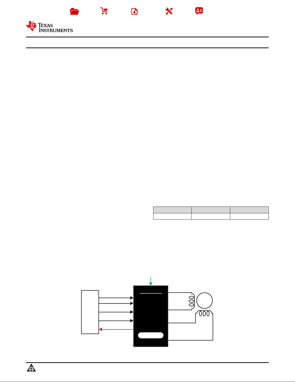
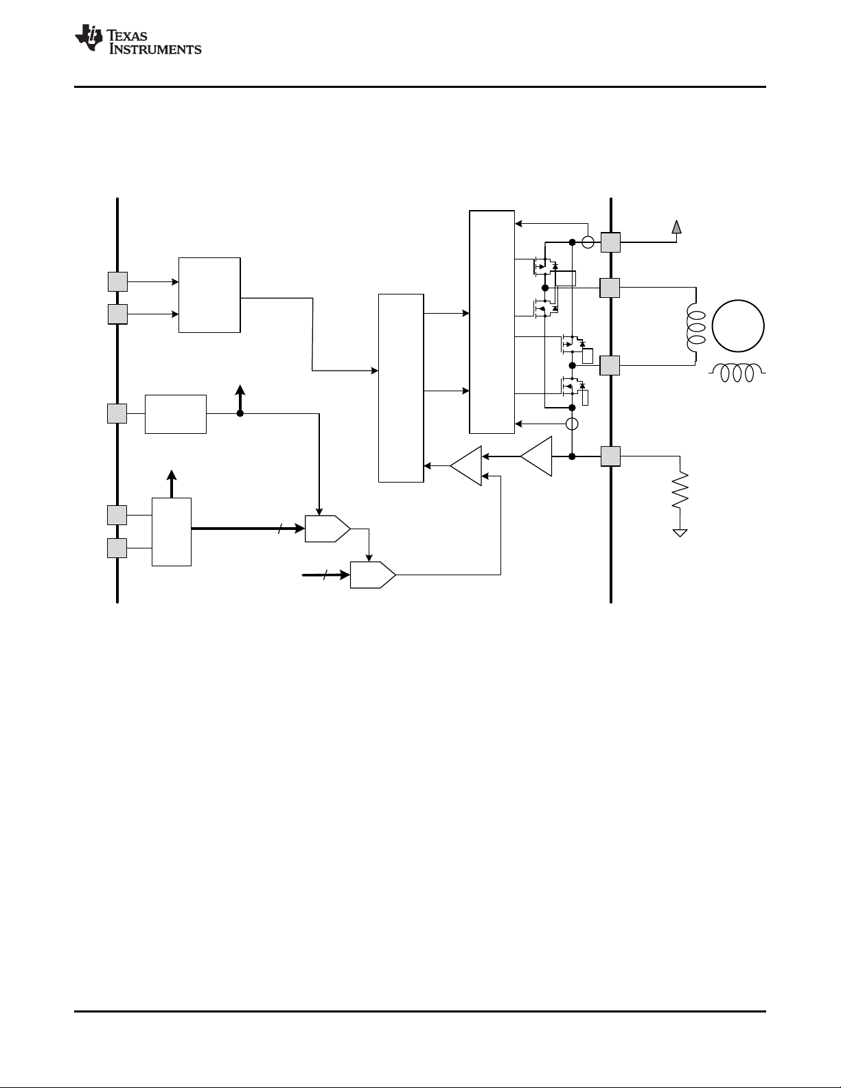
STEP/DIR
Step size
nFAULT
4 to 18 V
Controller
M
+ t
+ -
DRV8846
Stepper
Motor Driver
1 A
1 A
Decay Mode
1/32 µstep
Product
Folder
Sample &
Buy
Technical
Documents
Tools &
Software
Support &
Community
DRV8846 Dual H-Bridge Stepper Motor Driver
1 Features 3 Description
1
• PWM Microstepping Motor Driver
– Built-In Microstepping Indexer
– Up to 1/32 Microstepping
– Step/Direction Control
• Multiple Decay Modes
– Adaptive Decay
– Mixed Decay
– Slow Decay
– Fast Decay
• Configurable Off-Time PWM Chopping
– 10-, 20-, or 30-μs Off-Time
• Adaptive Blanking Time for Smooth Stepping
• 4- to 18-V Operating Supply Voltage Range
• 1-A Continuous/RMS Output Current per H-Bridge
(at 25°C)
• Low-Current Sleep Mode
• 3-Bit Torque DAC to Scale Motor Current
• Thermally Enhanced Surface Mount Package
• Protection Features
– VM Undervoltage Lockout (UVLO)
– Overcurrent Protection (OCP)
– Thermal Shutdown (TSD)
– Fault Condition Indication Pin (nFAULT)
2 Applications
• Printers
• Scanners
• Video Security Cameras
• Projectors
The DRV8846 provides a highly-integrated stepper
motor driver for cameras, printers, projectors, and
other automated equipment applications. The device
has two H-bridges and a microstepping indexer and
is intended to drive a bipolar stepper motor. The
output block of each H-bridge driver consists of Nchannel and P-channel power MOSFETs configured
as full H-bridges to drive the motor windings. The
DRV8846 is capable of driving up to 1-A full scale
output current (with proper heatsinking and TA=
25°C).
A simple STEP/DIR interface allows easy interfacing
to controller circuits. Pins allow configuration of the
motor in full-step up to 1/32-step modes. Decay mode
is configurable so that adaptive decay, slow decay,
fast decay, and mixed decay can be used. The PWM
current chopping off-time can also be selected. A lowpower sleep mode is provided which shuts down
internal circuitry to achieve very-low quiescent current
draw. This sleep mode can be set using a dedicated
nSLEEP pin.
Internal protection functions are provided for UVLO,
overcurrent protection, short circuit protection, and
overtemperature. Fault conditions are indicated via a
nFAULT pin.
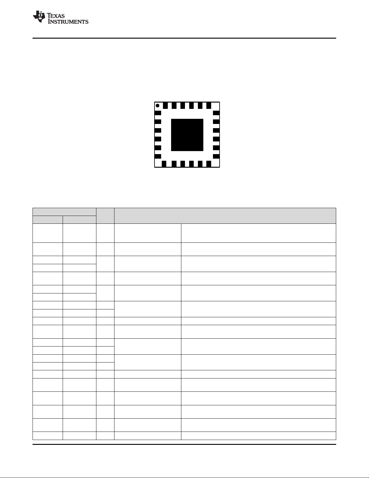
Device Information
PART NUMBER PACKAGE BODY SIZE (NOM)
DRV8846 QFN (24) 4.00 × 4.00 mm
(1) For all available packages, see the orderable addendum at
the end of the data sheet.
DRV8846
SLLSEK2 –JUNE 2014
(1)
4 Simplified Schematic
1
An IMPORTANT NOTICE at the end of this data sheet addresses availability, warranty, changes, use in safety-critical applications,
intellectual property matters and other important disclaimers. PRODUCTION DATA.
Page 2

DRV8846
SLLSEK2 –JUNE 2014
www.ti.com
Table of Contents
1 Features.................................................................. 1
2 Applications ........................................................... 1
3 Description ............................................................. 1
4 Simplified Schematic............................................. 1
5 Revision History..................................................... 2
6 Pin Configuration and Functions......................... 3
7 Specifications......................................................... 5
7.1 Absolute Maximum Ratings ...................................... 5
7.2 Handling Ratings....................................................... 5
7.3 Recommended Operating Conditions....................... 5
7.4 Thermal Information.................................................. 5
7.5 Electrical Characteristics........................................... 6
7.6 Timing Requirements................................................ 7
7.7 Typical Characteristics.............................................. 8
8 Detailed Description .............................................. 9
8.1 Overview ................................................................... 9
5 Revision History
DATE REVISION NOTES
June 2014 * Initial release.
8.2 Functional Block Diagram....................................... 10
8.3 Feature Description................................................. 11
8.4 Device Functional Modes........................................ 22
9 Application and Implementation........................ 23
9.1 Application Information............................................ 23
9.2 Typical Application ................................................. 23
10 Power Supply Recommendations ..................... 26
11 Layout................................................................... 26
11.1 Layout Guidelines ................................................. 26
11.2 Layout Example .................................................... 26
12 Device and Documentation Support................. 27
12.1 Trademarks ........................................................... 27
12.2 Electrostatic Discharge Caution............................ 27
12.3 Glossary ................................................................ 27
13 Mechanical, Packaging, and Orderable
Information........................................................... 27
2 Submit Documentation Feedback Copyright © 2014, Texas Instruments Incorporated
Product Folder Links: DRV8846
Page 3
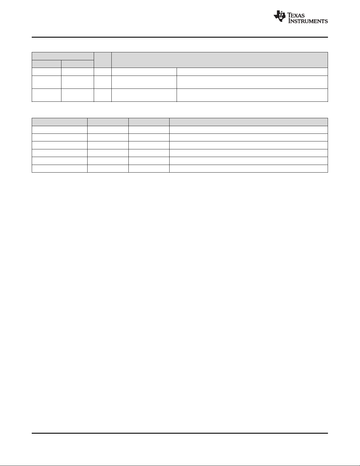
1
2
3
4
5
6
18
17
16
15
14
13
24
23
22
21
20
19
7
8
9
10
11
12
AOUT1
AISEN
AOUT2
BOUT2
BISEN
BOUT1
GND
VINT
NC
VM
VREF
DIR
nFAULT
M0
M1
nENBL
STEP
ADEC
I0
I1
DEC0
nSLEEP
DEC1
GND
(PPAD)
www.ti.com
6 Pin Configuration and Functions
DRV8846
SLLSEK2 –JUNE 2014
RGE (VQFN) Package
24 Pins
(Top View)
Pin Functions
PIN
NAME NO.
ADEC 19 I Adaptive decay enable adaptive decay operation is enabled; must be set prior to coming out
AISEN 2 O Winding A sense
AOUT1 1
AOUT2 3
BISEN 5 O Winding B sense
BOUT1 6
BOUT2 4
DEC0 22 I
DEC1 24 I
DIR 13 I Direction input Logic level sets the direction of stepping; internal pulldown
GND 18, PPAD PWR Device ground
I0 20 I
I1 21 I
MO 8 I
M1 9 I
NC 16 — No connect Unused pin not connected internally
nENBL 11 I Enable driver output
nFAULT 7 OD Fault indication pin
nSLEEP 23 I Sleep mode input
STEP 12 I Step input
TOFF_SEL 10 I Decay mode off time set Sets the off-time during current chopping; tri-level pin
Copyright © 2014, Texas Instruments Incorporated Submit Documentation Feedback 3
I/O DESCRIPTION
Logic low sets decay modes by DEC0 and DEC1 pins; logic high –
of sleep; internal pulldown
Connect to current sense resistor for bridge A, or GND if current
regulation is not required
O Winding A output
Connect to current sense resistor for bridge B, or GND if current
regulation is not required
O Winding B output
Decay mode setting pins Sets the decay mode; see description section; tri-level pin
Both the GND pin and device PowerPAD™ must be connected to
ground
Torque DAC current scalar Scales the current from 100% to 12.5% in 12.5% steps; tri-level pin
Microstepping mode setting Controls step mode (full, half, up to 1/32-step) and single- or dualpins edge clocking; tri-level pin
Logic low to enable device outputs and internal indexer; logic high to
disable; internal pulldown
Pulled logic low with fault condition; open-drain output requires
external pullup
Logic high to enable device; logic low to enter low-power sleep mode;
internal pulldown
A rising edge (or rising and falling depending on step mode) advances
the indexer one step; internal pulldown
Product Folder Links: DRV8846
Page 4
DRV8846
SLLSEK2 –JUNE 2014
www.ti.com
Pin Functions (continued)
PIN
NAME NO.
VINT 17 — Internal regulator Internal supply voltage; bypass to GND with 2.2-μF, 6.3-V capacitor
VM 15 PWR Power supply
VREF 14 I
I/O DESCRIPTION
Connect to motor power supply; bypass to GND with a 0.1- and 10-μF
(minimum) ceramic capacitor rated for VM
Full-scale current reference Voltage on this pin sets the full scale chopping current; short to VINT
input if not supplying an external reference voltage
Table 1. External Components
Component Pin 1 Pin 2 Recommended
C
VM
C
VM
C
VINT
R
nFAULT
R
AISEN
R
BISEN
(1) VCC is not a pin on the DRV8846, but a VCC supply voltage pullup is required for open-drain output nFAULT; nFAULT may be pulled
up to VINT through a resistor R
VM GND 10-µF (minimum) ceramic capacitor rated for VM
VM GND 0.1-µF ceramic capacitor rated for VM
VINT GND 6.3-V, 2.2-µF ceramic capacitor
(1)
VCC
nFAULT >5 kΩ
AISEN GND Sense resistor, see applications section for sizing
BISEN GND Sense resistor, see applications section for sizing
nFAULT
4 Submit Documentation Feedback Copyright © 2014, Texas Instruments Incorporated
Product Folder Links: DRV8846
Page 5
DRV8846
www.ti.com
SLLSEK2 –JUNE 2014
7 Specifications
7.1 Absolute Maximum Ratings
over operating free-air temperature referenced with respect to GND (unless otherwise noted)
Power supply voltage (VM) –0.3 20 V
Power supply voltage ramp rate (VM) 0 2 V/µs
Internal regulator voltage (VINT) –0.3 3.6 V
Analog input pin voltage (VREF) –0.3 3.6 V
Control pin voltage (nENABLE, STEP, DIR, I0, I1, M0, M1, DEC0, DEC1, TOFF_SEL, nSLEEP,
nFAULT, ADEC)
Continuous phase node pin voltage (AOUT1, AOUT2, BOUT1, BOUT2) –0.3 VM + 0.6 V
Continuous shunt amplifier input pin voltage (AISEN, BISEN)
(2)
Peak drive current (AOUT1, AOUT2, BOUT1, BOUT2, AISEN, BISEN) Internally limited A
T
Operating junction temperature –40 150 °C
J
(1) Stresses beyond those listed under Absolute Maximum Ratings may cause permanent damage to the device. These are stress ratings
only, which do not imply functional operation of the device at these or any other conditions beyond those indicated under Recommended
Operating Conditions. Exposure to absolute-maximum-rated conditions for extended periods may affect device reliability.
(2) Transients of ±1 V for less than 25 ns are acceptable.
7.2 Handling Ratings
T
V
(1) JEDEC document JEP155 states that 500-V HBM allows safe manufacturing with a standard ESD control process.
(2) JEDEC document JEP157 states that 250-V CDM allows safe manufacturing with a standard ESD control process.
Storage temperature range –65 150 °C
stg
(ESD)
Electrostatic
discharge
Human body model (HBM), per ANSI/ESDA/JEDEC JS-001, all pins
Charged device model (CDM), per JEDEC specification JESD22-C101, all pins
(1)
(1)
MIN MAX UNIT
–0.3 7.0 V
–0.6 0.6 V
MIN MAX UNIT
–4 4
(2)
–1.5 1.5
kV
7.3 Recommended Operating Conditions
over operating free-air temperature range (unless otherwise noted)
MIN MAX UNIT
VM Power supply voltage range
VREF Reference rms voltage range
ƒ
PWM
I
VINT
I
rms
T
A
(1) Note that R
(2) Operational at VREF between 0 to 1 V, but accuracy is degraded
Applied STEP signal 0 250 kHz
VINT external load current 1 mA
Motor rms current per H-bridge
Operating ambient temperature –40 85 °C
increases and maximum output current is reduced at VM supply voltages below 5 V
DS(ON)
(3) Power dissipation and thermal limits must be observed
(1)
(2)
(3)
4 18 V
1 3.3 V
0 1 A
7.4 Thermal Information
DRV8846
THERMAL METRIC
R
θJA
R
θJC(top)
R
θJB
ψ
JT
ψ
JB
R
θJC(bot)
Junction-to-ambient thermal resistance 34
Junction-to-case (top) thermal resistance 36.9
Junction-to-board thermal resistance 12.5
Junction-to-top characterization parameter 0.4
Junction-to-board characterization parameter 12.5
Junction-to-case (bottom) thermal resistance 2.5
(1) For more information about traditional and new thermal metrics, see the IC Package Thermal Metrics application report, SPRA953.
Copyright © 2014, Texas Instruments Incorporated Submit Documentation Feedback 5
(1)
Product Folder Links: DRV8846
QFN UNIT
24 PINS
°C/W
Page 6
DRV8846
SLLSEK2 –JUNE 2014
www.ti.com
7.5 Electrical Characteristics
TA= 25°C, over recommended operating conditions unless otherwise noted
PARAMETER TEST CONDITIONS MIN TYP MAX UNIT
POWER SUPPLIES (VM, VINT)
VM VM operating voltage 4 18 V
I
VM
I
VMQ
t
SLEEP
t
WAKE
t
ON
VM operating supply current 3.5 4.5 5.5 mA
VM sleep mode supply current VM = 12 V, nSLEEP = 0, nENBL = 0 or 1 0.5 1.2 3 μA
Sleep time nSLEEP = 0 to sleep mode 1 ms
Wake time nSLEEP = 1 to output transition 1 ms
Power-on time VM > V
VINT VINT voltage VM > 4 V, I
LOGIC-LEVEL INPUTS (STEP, DIR, nENBL, nSLEEP, ADEC)
V
IL
V
IH
V
HYS
I
IL
I
IH
R
PD
t
DEG
t
PROP
Input logic low voltage 0 0.7 V
Input logic high voltage 1.6 5.5 V
Input logic hysteresis 100 mV
Input logic low current VIN = 0 V –1 1 μA
Input logic high current VIN = 5 V 1 30 μA
Pulldown resistance kΩ
Input deglitch time 200 ns
Propagation delay STEP edge to current change 600 ns
TRI-LEVEL INPUTS (I0, I1, M0, M1, DEC0, DEC1, TOFF_SEL)
V
IL
V
IZ
V
IH
V
HYS
I
IL
I
IH
R
PD
R
PU
Tri-level input logic low voltage 0 0.7 V
Tri-level input Hi-Z voltage 1.1 V
Tri-level input logic high voltage 1.6 5.5 V
Tri-level input hysteresis 100 mV
Tri-level input logic low current VIN= 0 V –30 –1 μA
Tri-level input logic high current VIN= 5 V 1 30 μA
Tri-level pulldown resistance To GND 170 kΩ
Tri-level pullup resistance To VINT 340 kΩ
CONTROL OUTPUTS (nFAULT)
V
OL
I
OH
Output logic low voltage IO= 5 mA 0.5 V
Output logic high leakage VO= 3.3 V –1 1 μA
MOTOR DRIVER OUTPUTS (AOUT1, AOUT2, BOUT1, BOUT2)
R
DS(ON)
R
DS(ON)
I
OFF
t
RISE
t
FALL
t
DEAD
High-side FET on resistance Ω
Low-side FET on resistance Ω
Off-state leakage current VM = 5 V, TJ= 25°C –1 1 μA
Output rise time 60 ns
Output fall time 60 ns
Output dead time Internal dead time 200 ns
PWM CURRENT CONTROL (VREF, AISEN, BISEN)
I
REF
V
TRIP
A
ISENSE
Externally applied VREF input current VREF = 1 to 3.3 V 1 μA
xISEN trip voltage For 100% current step with VREF = 3.3 V 500 mV
Current sense amplifer gain Reference only 6.6 V/V
VM = 12 V, excluding winding current,
nSLEEP = 1, nENBL = 0 or 1
rising to output transition 1 ms
UVLO
= 0 A to 1 mA 3.13 3.3 3.47 V
OUT
nENBL, STEP, DIR, ADEC 200
nSLEEP 500
VM = 12 V, I = 0.5 A, TJ= 25°C 550
VM = 12 V, I = 0.5 A, TJ= 85°C
(1)
660
VM = 12 V, I = 0.5 A, TJ= 25°C 350
VM = 12 V, I = 0.5 A, TJ= 85°C
(1)
420
(1) Not tested in production; limits are based on characterization data
6 Submit Documentation Feedback Copyright © 2014, Texas Instruments Incorporated
Product Folder Links: DRV8846
Page 7
STEP
2
3
1
4
5
www.ti.com
SLLSEK2 –JUNE 2014
Electrical Characteristics (continued)
TA= 25°C, over recommended operating conditions unless otherwise noted
PARAMETER TEST CONDITIONS MIN TYP MAX UNIT
TOFF_SEL = GND 20
t
OFF
PROTECTION CIRCUITS
V
UVLO
I
OCP
t
OCP
t
RETRY
T
TSD
T
HYS
Current control constant off time TOFF_SEL = Hi-Z 10 μs
TOFF_SEL = VINT 30
VM undervoltage lockout V
VM falling; UVLO report 2.9
VM rising; UVLO recovery 3
Overcurrent protection trip level 2 A
Overcurrent deglitch time 2.8 μs
Overcurrent protection period 1.6 ms
Thermal shutdown temperature Die temperature T
Thermal shutdown hysteresis Die temperature T
J
J
150 160 180 °C
50 °C
7.6 Timing Requirements
TA= 25°C, over recommended operating conditions unless otherwise noted
NO. PARAMETER MIN MAX UNIT
1 ƒ
2 t
3 t
4 t
5 t
STEP
WH(STEP)
WL(STEP)
SU(STEP)
H(STEP)
Step frequency 250 kHz
Pulse duration, STEP high 1.9 μs
Pulse duration, STEP low 1.9 μs
Setup time, DIR or Mx to STEP rising 200 ns
Hold time, DIR or Mx to STEP rising 200 ns
DRV8846
Figure 1. Timing Diagram
Copyright © 2014, Texas Instruments Incorporated Submit Documentation Feedback 7
Product Folder Links: DRV8846
Page 8
VM (V)
R
DSON
HS + LS (:)
0 5 10 15 20
0
0.2
0.4
0.6
0.8
1
1.2
1.4
1.6
1.8
D001
-40qC
25qC
85qC
125qC
TA (qC)
R
DSON
HS + LS (:)
-50 0 50 100 150
0.6
0.8
1
1.2
1.4
1.6
1.8
D004
4 V
12 V
18 V
VM (V)
I
VM
(mA)
0 5 10 15 20
2
2.5
3
3.5
4
4.5
5
5.5
D001
-40qC
25qC
85qC
125qC
VM (V)
I
VMQ
(PA)
0 5 10 15 20
0
0.5
1
1.5
2
2.5
3
3.5
D001
-40qC
25qC
85qC
125qC
DRV8846
SLLSEK2 –JUNE 2014
7.7 Typical Characteristics
www.ti.com
Figure 2. IVMvs VM Figure 3. I
Figure 4. R
vs VM Figure 5. R
DSON
VMQ
vs Temperature
DSON
vs VM
8 Submit Documentation Feedback Copyright © 2014, Texas Instruments Incorporated
Product Folder Links: DRV8846
Page 9

DRV8846
www.ti.com
SLLSEK2 –JUNE 2014
8 Detailed Description
8.1 Overview
The DRV8846 is an integrated motor driver solution for bipolar stepper motors. The device integrates 2 H-bridges
that use NMOS low-side drivers and PMOS high-side drivers, current sense regulation circuitry, and a
microstepping indexer. The DRV8846 can be powered with a supply range between 4 to 18 V and is capable of
providing an output current to 1.4-A full scale or 1-A rms.
A simple STEP/DIR interface allows easy interfacing to the controller circuit. The internal indexer is able to
execute high-accuracy microstepping without requiring the processor to control the current level.
The PWM off-time, t
The DRV8846 has an adaptive decay feature that automatically adjusts the decay setting to minimize current
ripple while still reacting quickly to step changes. This feature allows the DRV8846 to quickly be integrated into a
system.
A torque DAC feature allows the controller to scale the output current without needing to scale the analog
reference voltage input VREF. The torque DAC is accessed using digital input pins. This allows the controller to
save power by decreasing the current consumption when not required.
A low-power sleep mode is included, which allows the system to save power when not driving the motor.
can be adjusted to 10, 20, or 30 μs.
OFF
Copyright © 2014, Texas Instruments Incorporated Submit Documentation Feedback 9
Product Folder Links: DRV8846
Page 10
OverTemp
AOUT1
GND
STEP
VM
Logic
AOUT2
VM
Gate
Drive
and
OCP
BOUT1
VM
BOUT2
VM
Gate
Drive
and
OCP
BISEN
AISEN
Step
Motor
ISEN
ISEN
DIR
M1
VM
VM
Internal Ref and
Regs
nFAULT
nSLEEP
nENBL
M0
10 µF
+
VM
I0
I1
PPAD
VINT
2.2 µF
VREF
DEC0
VREF
VREF
VINT
TOFF_SEL
DEC1
VINT
VINT
VINT
VINT
VINT
VINT
VINT
ADEC
DRV8846
SLLSEK2 –JUNE 2014
8.2 Functional Block Diagram
www.ti.com
10 Submit Documentation Feedback Copyright © 2014, Texas Instruments Incorporated
Product Folder Links: DRV8846
Page 11
xOUT1
xOUT2
VM
xISEN
Pre-
drive
VM
PWM
OCP
OCP
Optional
Step
Motor
SIN
DAC
5
+
±
DAC
3
I1
VREF
I0
A = 6.6
3level
Input
buffer
To other
channel
From Indexer
Internal
reference
To other
channel
DIR
STEP
Indexer
DRV8846
www.ti.com
SLLSEK2 –JUNE 2014
8.3 Feature Description
8.3.1 PWM Motor Drivers
DRV8846 contains two identical H-bridge motor drivers with current-control PWM circuitry. Figure 6 shows a
block diagram of the circuitry.
Figure 6. PWM Motor Driver Circuitry
8.3.2 Micro-Stepping Indexer
To allow a simple step and direction interface to control stepper motors, the DRV8846 contains a microstepping
indexer. The indexer controls the state of the H-bridges automatically. When the correct transition is applied at
the STEP input, the indexer moves to the next step, according to the direction set by the DIR pin. In 1/8, 1/16,
and 1/32 step modes, both the rising and falling edges of the STEP input may be used to advance the indexer,
depending on the M0 / M1 setting.
The nENBL pin disables the output stage in indexer mode. When nENBL = 0, the indexer inputs are still active
and respond to the STEP and DIR input pins; only the output stage is disabled.
The indexer logic in the DRV8846 allows a number of different stepping configurations. The M0 and M1 pins
configure the stepping format (see Table 2).
Copyright © 2014, Texas Instruments Incorporated Submit Documentation Feedback 11
Product Folder Links: DRV8846
Page 12

DRV8846
SLLSEK2 –JUNE 2014
www.ti.com
Table 2. Step Mode Settings
M1 M0 STEP MODE
0 0 Full step (2-phase excitation), rising-edge only
0 Z 1/2 step (1-2 phase excitation), rising-edge only
0 1 1/4 step (W1-2 phase excitation), rising-edge only
Z 0 8 microsteps/step, rising-edge only
Z Z 8 microsteps/step, rising and falling edges
Z 1 16 microsteps/step, rising-edge only
1 0 16 microsteps/step, rising and falling edges
1 Z 32 microsteps/step, rising-edge only
1 1 32 microsteps/step, rising and falling edges
Note that the M0 and M1 pins are tri-level inputs. These pins can be driven logic low, logic high, or highimpedance (Z), like the I0 and I1 pins described previously.
For 1/8, 1/16, and 1/32-step modes, selections are available to advance the indexer only on the rising edge of
the STEP input, or on both the rising and falling edges.
The step mode may be changed on-the-fly while the motor is moving. The indexer advances to the next valid
state for the new M0 / M1 setting at the next rising edge of STEP.
The home state is 45°. The indexer enters the home state after power-up, after exiting UVLO, or after exiting
sleep mode (see the yellow-shaded cells in Table 3 also indicated with a table note).
Table 3 shows the relative current and step directions for different step mode settings. At each rising edge of the
STEP input, the indexer travels to the next state in the table. The direction is shown with the DIR pin high; if the
DIR pin is low, the sequence is reversed. Positive current is defined as xOUT1 = positive with respect to xOUT2.
Table 3. Relative Current and Step Directions
1/32 STEP 1/16 STEP 1/8 STEP 1/4 STEP 1/2 STEP
1 1 1 1 1 100% 0% 0
2 100% 5% 3
3 2 100% 10% 6
4 99% 15% 8
5 3 2 98% 20% 11
6 97% 24% 14
7 4 96% 29% 17
8 94% 34% 20
9 5 3 2 92% 38% 23
10 90% 43% 25
11 6 88% 47% 28
12 86% 51% 31
13 7 4 83% 56% 34
14 80% 60% 37
15 8 77% 63% 39
16 74% 67% 42
(1)
17
18 67% 74% 48
19 10 63% 77% 51
20 60% 80% 53
21 11 6 56% 83% 56
22 51% 86% 59
(1)
9
(1)
5
(1)
3
(1)
2
FULL STEP WINDING WINDING ELECTRICAL
70% CURRENT A CURRENT B ANGLE
(1)
1
71% 71% 45
(1) The indexer enters the home state after power-up, after exiting UVLO, or after exiting sleep mode.
12 Submit Documentation Feedback Copyright © 2014, Texas Instruments Incorporated
Product Folder Links: DRV8846
Page 13

www.ti.com
Table 3. Relative Current and Step Directions (continued)
1/32 STEP 1/16 STEP 1/8 STEP 1/4 STEP 1/2 STEP
23 12 47% 88% 62
24 43% 90% 65
25 13 7 4 38% 92% 68
26 34% 94% 70
27 14 29% 96% 73
28 24% 97% 76
29 15 8 20% 98% 79
30 15% 99% 82
31 16 10% 100% 84
32 5% 100% 87
33 17 9 5 3 0% 100% 90
34 –5% 100% 93
35 18 –10% 100% 96
36 –15% 99% 98
37 19 10 –20% 98% 101
38 –24% 97% 104
39 20 –29% 96% 107
40 –34% 94% 110
41 21 11 6 –38% 92% 113
42 –43% 90% 115
43 22 –47% 88% 118
44 –51% 86% 121
45 23 12 –56% 83% 124
46 –60% 80% 127
47 24 –63% 77% 129
48 –67% 74% 132
49 25 13 7 4 2 –71% 71% 135
50 –74% 67% 138
51 26 –77% 63% 141
52 –80% 60% 143
53 27 14 –83% 56% 146
54 –86% 51% 149
55 28 –88% 47% 152
56 –90% 43% 155
57 29 15 8 –92% 38% 158
58 –94% 34% 160
59 30 –96% 29% 163
60 –97% 24% 166
61 31 16 –98% 20% 169
62 –99% 15% 172
63 32 –100% 10% 174
64 –100% 5% 177
65 33 17 9 5 –100% 0% 180
66 –100% –5% 183
67 34 –100% –10% 186
68 –99% –15% 188
69 35 18 –98% –20% 191
FULL STEP WINDING WINDING ELECTRICAL
70% CURRENT A CURRENT B ANGLE
DRV8846
SLLSEK2 –JUNE 2014
Copyright © 2014, Texas Instruments Incorporated Submit Documentation Feedback 13
Product Folder Links: DRV8846
Page 14

DRV8846
SLLSEK2 –JUNE 2014
Table 3. Relative Current and Step Directions (continued)
1/32 STEP 1/16 STEP 1/8 STEP 1/4 STEP 1/2 STEP
70 –97% –24% 194
71 36 –96% –29% 197
72 –94% –34% 200
73 37 19 10 –92% –38% 203
74 –90% –43% 205
75 38 –88% –47% 208
76 –86% –51% 211
77 39 20 –83% –56% 214
78 –80% –60% 217
79 40 –77% –63% 219
80 –74% –67% 222
81 41 21 11 6 3 –71% –71% 225
82 –67% –74% 228
83 42 –63% –77% 231
84 –60% –80% 233
85 43 22 –56% –83% 236
86 –51% –86% 239
87 44 –47% –88% 242
88 –43% –90% 245
89 45 23 12 –38% –92% 248
90 –34% –94% 250
91 46 –29% –96% 253
92 –24% –97% 256
93 47 24 –20% –98% 259
94 –15% –99% 262
95 48 –10% –100% 264
96 –5% –100% 267
97 49 25 13 7 0% –100% 270
98 5% –100% 273
99 50 10% –100% 276
100 15% –99% 278
101 51 26 20% –98% 281
102 24% –97% 284
103 52 29% –96% 287
104 34% –94% 290
105 53 27 14 38% –92% 293
106 43% –90% 295
107 54 47% –88% 298
108 51% –86% 301
109 55 28 56% –83% 304
110 60% –80% 307
111 56 63% –77% 309
112 67% –74% 312
113 57 29 15 8 4 71% –71% 315
114 74% –67% 318
115 58 77% –63% 321
116 80% –60% 323
FULL STEP WINDING WINDING ELECTRICAL
70% CURRENT A CURRENT B ANGLE
www.ti.com
14 Submit Documentation Feedback Copyright © 2014, Texas Instruments Incorporated
Product Folder Links: DRV8846
Page 15

FS
ISENSE
VREF
6.6 R
u
u
DRV8846
www.ti.com
SLLSEK2 –JUNE 2014
Table 3. Relative Current and Step Directions (continued)
1/32 STEP 1/16 STEP 1/8 STEP 1/4 STEP 1/2 STEP
117 59 30 83% –56% 326
118 86% –51% 329
119 60 88% –47% 332
120 90% –43% 335
121 61 31 16 92% –38% 338
122 94% –34% 340
123 62 96% –29% 343
124 97% –24% 346
125 63 32 98% –20% 349
126 99% –15% 352
127 64 100% –10% 354
128 100% –5% 357
FULL STEP WINDING WINDING ELECTRICAL
70% CURRENT A CURRENT B ANGLE
8.3.3 Current Regulation
The current through the motor windings is regulated by an adjustable fixed-off-time PWM current regulation
circuit. When an H-bridge is enabled, current rises through the winding at a rate dependent on the DC voltage,
inductance of the winding, and the magnitude of the back EMF present. After the current reaches the current
chopping threshold, the bridge enters a decay mode for a fixed period of time to decrease the current, which is
configurable between 10 to 30 µs through the tri-level input TOFF_SEL. After the time expires, the bridge is reenabled, starting another PWM cycle.
Table 4. Fixed Off-Time Selection
TOFF_SEL TOFF Duration
0 20 μs
Z 10 μs
1 30 μs
The PWM chopping current is set by a comparator which compares the voltage across a current sense resistor
connected to the xISEN pin, with a reference voltage. The reference voltage can be supplied by an internal
reference of 3.3 V (which requires VINT to be connected to VREF), or externally supplied to the VREF pin. The
reference voltage is then scaled first by the 3-bit torque DAC, then by the output of a sine lookup table that is
applied to a sine-weighted DAC (sine DAC). The voltage is attenuated by a factor of 6.6.
The full-scale (100%) chopping current is calculated as follows:
where
• IFSis the full scale regulated current
• VREF is the voltage on the VREF pin
• R
is the resistance of the sense resistor
ISENSE
• TORQUE is the scaling percentage from the torque DAC. (1)
Example: Using VREF is 3.3 V, torque DAC = 100%, and a 500-mΩ sense resistor, the full-scale chopping
current is 3.3 V / (6.6 × 500 mΩ) × 100% = 1 A.
The current for both motor windings is scaled depending on the I0 and I1 pins, which drive a 3-bit linear DAC, as
in Table 5.
Copyright © 2014, Texas Instruments Incorporated Submit Documentation Feedback 15
Product Folder Links: DRV8846
Page 16

DRV8846
SLLSEK2 –JUNE 2014
Table 5. Torque DAC Settings
I1 I0 CURRENT SCALING (TORQUE)
0 0 100%
0 Z 87.5%
0 1 75%
Z 0 62.5%
Z Z 50%
Z 1 37.5%
1 0 25%
1 Z 12.5%
1 1 0% (outputs disabled)
Table 6 gives the xISEN trip voltage at a given DAC code and I[1:0] setting.
Table 6. Torque DAC xISENS Trip Levels (VREF = 3.3 V)
Sine DAC
Code
31 500 mV 438 mV 375 mV 313 mV 250 mV 188 mV 125 mV 63 mV
30 500 mV 438 mV 375 mV 313 mV 250 mV 188 mV 125 mV 63 mV
29 495 mV 433 mV 371 mV 309 mV 248 mV 186 mV 124 mV 62 mV
28 490 mV 429 mV 368 mV 306 mV 245 mV 184 mV 123 mV 61 mV
27 485 mV 424 mV 364 mV 303 mV 243 mV 182 mV 121 mV 61 mV
26 480 mV 420 mV 360 mV 300 mV 240 mV 180 mV 120 mV 60 mV
25 470 mV 411 mV 353 mV 294 mV 235 mV 176 mV 118 mV 59 mV
24 460 mV 403 mV 345 mV 288 mV 230 mV 173 mV 115 mV 58 mV
23 450 mV 394 mV 338 mV 281 mV 225 mV 169 mV 113 mV 56 mV
22 440 mV 385 mV 330 mV 275 mV 220 mV 165 mV 110 mV 55 mV
21 430 mV 376 mV 323 mV 269 mV 215 mV 161 mV 108 mV 54 mV
20 415 mV 363 mV 311 mV 259 mV 208 mV 156 mV 104 mV 52 mV
19 400 mV 350 mV 300 mV 250 mV 200 mV 150 mV 100 mV 50 mV
18 385 mV 337 mV 289 mV 241 mV 193 mV 144 mV 96 mV 48 mV
17 370 mV 324 mV 278 mV 231 mV 185 mV 139 mV 93 mV 46 mV
16 355 mV 311 mV 266 mV 222 mV 178 mV 133 mV 89 mV 44 mV
15 335 mV 293 mV 251 mV 209 mV 168 mV 126 mV 84 mV 42 mV
14 315 mV 276 mV 236 mV 197 mV 158 mV 118 mV 79 mV 39 mV
13 300 mV 263 mV 225 mV 188 mV 150 mV 113 mV 75 mV 38 mV
12 280 mV 245 mV 210 mV 175 mV 140 mV 105 mV 70 mV 35 mV
11 255 mV 223 mV 191 mV 159 mV 128 mV 96 mV 64 mV 32 mV
10 235 mV 206 mV 176 mV 147 mV 118 mV 88 mV 59 mV 29 mV
9 215 mV 188 mV 161 mV 134 mV 108 mV 81 mV 54 mV 27 mV
8 190 mV 166 mV 143 mV 119 mV 95 mV 71 mV 48 mV 24 mV
7 170 mV 149 mV 128 mV 106 mV 85 mV 64 mV 43 mV 21 mV
6 145 mV 127 mV 109 mV 91 mV 73 mV 54 mV 36 mV 18 mV
5 120 mV 105 mV 90 mV 75 mV 60 mV 45 mV 30 mV 15 mV
4 100 mV 88 mV 75 mV 63 mV 50 mV 38 mV 25 mV 13 mV
3 75 mV 66 mV 56 mV 47 mV 38 mV 28 mV 19 mV 9 mV
2 50 mV 44 mV 38 mV 31 mV 25 mV 19 mV 13 mV 6 mV
1 25 mV 22 mV 19 mV 16 mV 13 mV 9 mV 6 mV 3 mV
0 0 mV 0 mV 0 mV 0 mV 0 mV 0 mV 0 mV 0 mV
00 - 100% 0Z - 87.5% 01 - 75% Z0 - 62.5% ZZ - 50% Z1 - 37.5% 10 - 25% 1Z - 12.5%
Torque DAC I[1:0] Setting
www.ti.com
16 Submit Documentation Feedback Copyright © 2014, Texas Instruments Incorporated
Product Folder Links: DRV8846
Page 17

xOUT1
xOUT2
1
2
3
Drive Current
Slow decay
Fast decay
xVM
1
2
3
DRV8846
www.ti.com
SLLSEK2 –JUNE 2014
8.3.4 Decay Mode
After the chopping current threshold is reached, the drive current is interrupted, but due to the inductive nature of
the motor, current must continue to flow for some period of time (called recirculation current). To handle this
recirculation current, the H-bridge can operate in two different states, fast decay or slow decay (or a mixture of
fast and slow decay).
In fast-decay mode, after the PWM chopping current level is reached, the H-bridge reverses state to allow
winding current to flow through the opposing FETs. As the winding current approaches 0, the bridge is disabled
to prevent any reverse current flow. For fast-decay mode, see number 2 in Figure 7.
In slow-decay mode, winding current is recirculated by enabling both of the low-side FETs in the bridge. For
slow-decay mode, see number 3 in Figure 7.
Figure 7. Decay Modes
The DRV8846 supports fast, slow, mixed, and adaptive decay modes. With stepper motors, the decay mode is
chosen for a given stepper motor and operating conditions to minimize mechanical noise and vibration.
In mixed decay mode, the current recirculation begins as fast decay, but at a fixed period of time (determined by
the state of the DEC1 and DEC0 pins shown in Table 7) the current recirculation switches to slow decay mode
for the remainder of the fixed PWM period. Note that the DEC1 and DEC0 pins are tri-level inputs; these pins
can be driven logic low, logic high, or high-impedance (Z).
Figure 8 shows the current waveforms in slow, fast, and 25% and 1 t
Copyright © 2014, Texas Instruments Incorporated Submit Documentation Feedback 17
Product Folder Links: DRV8846
mixed decay modes.
BLANK
Page 18

Slow Decay
Fast Decay
25%
1 t
BLANK
PWM
ON
PWM OFF (t
OFF
)
PWM CYCLE
25% of cycle
1 t
BLANK
Itrip
DRV8846
SLLSEK2 –JUNE 2014
www.ti.com
Figure 8. Decay Behavior
Table 7. Decay Pins Configuration
DEC1 DEC0 Decay Mode (Increasing Current) Decay Mode (Decreasing Current)
0 0 Slow decay Slow decay
0 Z Slow decay Mixed decay: 25% fast
0 1 Slow decay Mixed decay: 1 t
Z 0 Mixed decay: 1 t
Z Z Mixed decay: 50% fast Mixed decay: 50% fast
Z 1 Mixed decay: 25% fast Mixed decay: 25% fast
1 0 Slow decay Mixed decay: 50% fast
1 Z Slow decay Mixed decay: 12.5% fast
1 1 Slow decay Fast decay
BLANK
BLANK
Mixed decay: 1 t
BLANK
18 Submit Documentation Feedback Copyright © 2014, Texas Instruments Incorporated
Product Folder Links: DRV8846
Page 19

t
BLANK
t
ON
t
OFF
(fixed)
t
BLANK
t
ON
t
OFF
(fixed)
t
BLANK
t
ON
t
OFF
(fixed)
FET Drive On (FWD or REV)
Slow Decay
AOUT Current
STEP Input
Increasing
Decreasing
Increasing
Decreasing
BOUT Current
STEP Input
Decreasing
Increasing
Decreasing
Increasing
DRV8846
www.ti.com
SLLSEK2 –JUNE 2014
Figure 9 shows increasing and decreasing current. When current is decreasing, the decay mode used is fast,
slow, or mixed as commanded by the DEC1 and DEC0 pins. Three DEC pin selections allow for mixed decay
during increasing current.
Adaptive decay mode simplifies the decay mode selection by dynamically changing to adjust for current level,
step change, supply variation, BEMF, and load. To enable adaptive decay mode, pull the ADEC pin to logic high
and pull DEC0 and DEC1 pins to logic high. The state of the ADEC pin is only evaluated when exiting sleep
mode.
Adaptive decay adjusts the time spent in fast decay to minimize current ripple and quickly adjust to current-step
changes. If the drive time is longer than the minimum (t
mode applied is slow decay (see Figure 10).
Copyright © 2014, Texas Instruments Incorporated Submit Documentation Feedback 19
Figure 9. Increasing and Decreasing Current
), in order to reach the current trip point, the decay
BLANK
Figure 10. Adaptive Decay – Slow Decay Operation
Product Folder Links: DRV8846
Page 20

t
BLANK
t
BLANK
t
OFF
(fixed)
t
BLANK
t
BLANK
t
OFF
(fixed) t
BLANK
t
BLANK
t
OFF
(fixed)
t
BLANK
t
OFF
(fixed)
t
BLANK
t
BLANK
t
BLANK
t
off
25%
t
BLANK
STEP
Slow Decay
Fast Decay
FET Drive On (FWD or REV)
t
BLANK
t
off
25%
t
BLANK
t
off
25%
t
BLANK
t
BLANK
t
OFF
(fixed)
t
BLANK
t
BLANK
t
BLANK
t
OFF
(fixed) t
BLANK
t
off
25%
t
OFF
(fixed)
t
OFF
(fixed)
t
BLANK
Slow Decay
Fast Decay
FET Drive On (FWD or REV)
DRV8846
SLLSEK2 –JUNE 2014
www.ti.com
When the minimum drive time (t
applied. If the second drive period also provides more current than the regulation point, fast decay of 2 t
) provides more current than the regulation point, fast decay of 1- t
BLANK
BLANK
BLANK
applied. If a third (or more) consecutive period provides more current than the regulation point, fast decay using
25% of t
time is applied. When the minimum drive time is insufficient to reach the current regulation level,
OFF
slow decay is applied until the current exceeds the current reference level (see Figure 11).
Figure 11. Adaptive Decay – Mixed Decay Operation
Figure 12 shows a case for adaptive decay where a step occurs. The system starts with 1 t
and works up to 25% of t
time for fast decay until the current is regulated again.
OFF
BLANK
of fast decay
is
is
8.3.5 Blanking Time
After the current is enabled in an H-bridge, the voltage on the xISEN pin is ignored for a period of time before
enabling the current sense circuitry. Note that the blanking time also sets the minimum drive time of the PWM.
The time, t
t
BLANK
20 Submit Documentation Feedback Copyright © 2014, Texas Instruments Incorporated
BLANK
is given in Table 8.
Figure 12. Adaptive Decay – Step Operation
, is determined by the sine DAC code and the torque DAC setting. The timing information for
Product Folder Links: DRV8846
Page 21

www.ti.com
DRV8846
SLLSEK2 –JUNE 2014
Table 8. t
Sine DAC
Code
31 1.80 µs 1.80 µs 1.50 µs 1.50 µs 1.50 µs 1.20 µs 1.20 µs 0.90 µs
30 1.80 µs 1.80 µs 1.50 µs 1.50 µs 1.50 µs 1.20 µs 1.20 µs 0.90 µs
29 1.80 µs 1.80 µs 1.50 µs 1.50 µs 1.50 µs 1.20 µs 1.20 µs 0.90 µs
28 1.80 µs 1.80 µs 1.50 µs 1.50 µs 1.50 µs 1.20 µs 1.20 µs 0.90 µs
27 1.80 µs 1.80 µs 1.50 µs 1.50 µs 1.50 µs 1.20 µs 1.20 µs 0.90 µs
26 1.80 µs 1.80 µs 1.50 µs 1.50 µs 1.50 µs 1.20 µs 1.20 µs 0.90 µs
25 1.80 µs 1.80 µs 1.50 µs 1.50 µs 1.50 µs 1.20 µs 1.20 µs 0.90 µs
24 1.80 µs 1.80 µs 1.50 µs 1.50 µs 1.50 µs 1.20 µs 1.20 µs 0.90 µs
23 1.80 µs 1.80 µs 1.50 µs 1.50 µs 1.50 µs 1.20 µs 1.20 µs 0.90 µs
22 1.80 µs 1.80 µs 1.50 µs 1.50 µs 1.50 µs 1.20 µs 1.20 µs 0.90 µs
21 1.80 µs 1.80 µs 1.50 µs 1.50 µs 1.50 µs 1.20 µs 1.20 µs 0.90 µs
20 1.80 µs 1.80 µs 1.50 µs 1.50 µs 1.50 µs 1.20 µs 1.20 µs 0.90 µs
19 1.80 µs 1.80 µs 1.50 µs 1.50 µs 1.50 µs 1.20 µs 1.20 µs 0.90 µs
18 1.80 µs 1.80 µs 1.50 µs 1.50 µs 1.50 µs 1.20 µs 1.20 µs 0.90 µs
17 1.80 µs 1.80 µs 1.50 µs 1.50 µs 1.50 µs 1.20 µs 1.20 µs 0.90 µs
16 1.80 µs 1.80 µs 1.50 µs 1.50 µs 1.50 µs 1.20 µs 1.20 µs 0.90 µs
15 1.50 µs 1.50 µs 1.50 µs 1.20 µs 1.20 µs 1.20 µs 0.90 µs 0.90 µs
14 1.50 µs 1.50 µs 1.50 µs 1.20 µs 1.20 µs 1.20 µs 0.90 µs 0.90 µs
13 1.50 µs 1.50 µs 1.50 µs 1.20 µs 1.20 µs 1.20 µs 0.90 µs 0.90 µs
12 1.50 µs 1.50 µs 1.50 µs 1.20 µs 1.20 µs 1.20 µs 0.90 µs 0.90 µs
11 1.50 µs 1.50 µs 1.50 µs 1.20 µs 1.20 µs 1.20 µs 0.90 µs 0.90 µs
10 1.50 µs 1.50 µs 1.50 µs 1.20 µs 1.20 µs 1.20 µs 0.90 µs 0.90 µs
9 1.50 µs 1.50 µs 1.50 µs 1.20 µs 1.20 µs 1.20 µs 0.90 µs 0.90 µs
8 1.50 µs 1.50 µs 1.50 µs 1.20 µs 1.20 µs 1.20 µs 0.90 µs 0.90 µs
7 1.20 µs 1.20 µs 1.20 µs 0.90 µs 0.90 µs 0.90 µs 0.90 µs 0.90 µs
6 1.20 µs 1.20 µs 1.20 µs 0.90 µs 0.90 µs 0.90 µs 0.90 µs 0.90 µs
5 1.20 µs 1.20 µs 1.20 µs 0.90 µs 0.90 µs 0.90 µs 0.90 µs 0.90 µs
4 1.20 µs 1.20 µs 1.20 µs 0.90 µs 0.90 µs 0.90 µs 0.90 µs 0.90 µs
3 0.90 µs 0.90 µs 0.90 µs 0.90 µs 0.90 µs 0.90 µs 0.90 µs 0.90 µs
2 0.90 µs 0.90 µs 0.90 µs 0.90 µs 0.90 µs 0.90 µs 0.90 µs 0.90 µs
1 0.90 µs 0.90 µs 0.90 µs 0.90 µs 0.90 µs 0.90 µs 0.90 µs 0.90 µs
0 0.90 µs 0.90 µs 0.90 µs 0.90 µs 0.90 µs 0.90 µs 0.90 µs 0.90 µs
00 - 100% 0Z - 87.5% 01 - 75% Z0 - 62.5% ZZ - 50% Z1 - 37.5% 10 - 25% 1Z - 12.5%
Torque DAC I[1:0] Setting
BLANK
Settings
8.3.6 Protection Circuits
The DRV8846 is fully protected against undervoltage, overcurrent, and overtemperature events.
8.3.6.1 Overcurrent Protection (OCP)
An analog current limit circuit on each FET limits the current through the FET by limiting the gate drive. If this
analog current limit persists for longer than the OCP deglitch time t
the nFAULT pin is driven low. The device remains disabled until the retry time, t
, all FETs in the H-bridge are disabled and
OCP
, occurs. The OCP is
RETRY
independent for each H-bridge.
Overcurrent conditions are detected independently on both high-side and low-side devices; that is, a short to
ground, supply, or across the motor winding all result in an OCP event. Note that OCP does not use the current
sense circuitry used for PWM current control, so OCP functions without the presence of the xISEN resistors.
Copyright © 2014, Texas Instruments Incorporated Submit Documentation Feedback 21
Product Folder Links: DRV8846
Page 22

DRV8846
SLLSEK2 –JUNE 2014
www.ti.com
8.3.6.2 Thermal Shutdown (TSD)
If the die temperature exceeds safe limits, all FETs in the H-bridge are disabled and the nFAULT pin is driven
low. After the die temperature falls to a safe level, operation automatically resumes. The nFAULT pin is released
after operation has resumed.
8.3.6.3 Undervoltage Lockout (UVLO)
If at any time the voltage on the VM pin falls below the UVLO falling threshold voltage, V
, all circuitry in the
UVLO
device is disabled, and all internal logic is reset. Operation resumes when VM rises above the UVLO rising
threshold. The nFAULT pin is driven low during an undervoltage condition and is released after operation has
resumed.
Table 9. Fault Behavior
Fault Error Report H-Bridge Internal Circuits Recovery
VM UVLO nFAULT unlatched Disabled Shut down System and fault clears on recovery
OCP nFAULT unlatched Disabled Operating
TSD nFAULT unlatched Disabled Operating System and fault clears on recovery
System and fault clears on recovery and motor is driven
after time, t
RETRY
8.4 Device Functional Modes
The DRV8846 device is active unless the nSLEEP pin is driven low. In sleep mode, the VINT regulator is
disabled and the H-bridge FETs are disabled (Hi-Z). The time t
nSLEEP pin before the device enters sleep mode. The DRV8846 is brought out of sleep mode by bringing the
nSLEEP pin high. The time t
must elapse, after nSLEEP is brought high, before the outputs change state.
WAKE
If the nENBL pin is brought high, the H-bridge outputs are disabled, but the internal logic is still active. An
appropriate edge on STEP (depending on the step mode) advances the indexer, but the outputs do not change
state until nENBL is driven low.
When VM falls below the VM UVLO threshold, V
, the output driver, internal logic, and VINT regulator are
UVLO
reset.
must elapse after a falling edge on the
SLEEP
Table 10. Operating Modes
Mode Condition H-Bridge VINT Indexer
Operating nSLEEP pin = 1 Operating Operating Operating
Disabled nSLEEP pin = 1 Disabled Operating Operating
Sleep Disabled Disabled Disabled
Fault Any fault condition met Disabled Depends on fault Depends on fault
4 V < VM < 18 V
nENBL = 0
4 V < VM < 18 V
nENBL = 1
4 V < VM < 18 V
nSLEEP pin = 0
22 Submit Documentation Feedback Copyright © 2014, Texas Instruments Incorporated
Product Folder Links: DRV8846
Page 23

AOUT1
AISEN
AOUT2
BOUT2
BISEN
BOUT1
nFAULT
M0
M1
TOFF_SEL
nENBL
STEP
GND
VINT
NC
VM
VREF
DIR
DEC1
nSLEEP
DEC0
I1
I0
ADEC
Step
Motor
DRV8846
VM
18
17
16
15
14
13
VCC
logic supply
500 P
500 P
10 N
GND
(PPAD)
2.2 µF
10 µF
0.1 µF
DRV8846
www.ti.com
SLLSEK2 –JUNE 2014
9 Application and Implementation
9.1 Application Information
The DRV8846 is used in stepper motor control. The following design procedure can be used to configure the
DRV8846.
9.2 Typical Application
9.2.1 Design Requirements
Table 11 gives design input parameters for system design.
Nominal supply voltage 12 V
Supply voltage range 4 to 18 V
Motor winding resistance R
Motor winding inductance L
Motor full step angle θ
Design Parameter Reference Example Value
Table 11. System Design Input Parameters
VM
step
L
L
3.0 Ω/phase
330 µH/phase
1.8°/step
Target stepping level nm 1/8 step
Target motor speed v 400 rpm
Target chopping current I
Chopping current reference voltage VREF 3.3 V
CHOP
500 mA
Current scaling TORQUE 100%
Copyright © 2014, Texas Instruments Incorporated Submit Documentation Feedback 23
Product Folder Links: DRV8846
Page 24

CHOP
L DS(ON) SENSE
VM (V)
R ( ) 2 R ( ) R ( )
: u : :
CHOP
ISENSE
VREF
6.6 R
u
u
m
step
step
v(rpm) n (steps) 6
¦ VWHSV V
( / step)
u u
T q
DRV8846
SLLSEK2 –JUNE 2014
www.ti.com
9.2.2 Detailed Design Procedure
9.2.2.1 Stepper Motor Speed
The first step in configuring the DRV8846 requires the desired motor speed and stepping level. The DRV8846
can support from full step to 1/32 step mode.
If the target motor speed is too high, the motor will not spin. Make sure that the motor can support the target
speed.
For a desired motor speed (v), microstepping level (nm), and motor full step angle (θ
θ
can be found in the stepper motor data sheet or often written on the motor itself.
step
step
),
(2)
For DRV8846, the microstepping levels are set by the M0/M1 pins and can be any of the settings in Table 2.
Higher microstepping means a smoother motor motion and less audible noise, but increases the switching losses
and requires a higher ƒ
to achieve the same motor speed.
step
9.2.2.2 Current Regulation
The chopping current (I
the sense resistor value (R
) is the maximum current driven through either winding. This quantity will depend on
CHOP
XISEN
).
(3)
I
is set by a comparator which compares the voltage across R
CHOP
to a reference voltage. Note that I
XISEN
CHOP
must follow Equation 4 to avoid saturating the motor.
where
• VM is the motor supply voltage.
• RLis the motor winding resistance. (4)
9.2.2.3 Decay Modes
The DRV8846 supports four different decay modes: slow decay, fast decay, mixed decay, and adaptive decay.
The first selection to try is the adaptive decay mode, which adjusts the decay mode automatically to improve
current regulation. The current through the motor windings is regulated using a fixed-off-time PWM scheme. This
means that after any drive phase, when a motor has reached the current chopping threshold (I
CHOP
), the
DRV8846 places the motor in one of the four decay modes until the PWM cycle has expired. Afterward, a new
drive phase starts.
The blanking time, t
, defines the minimum drive time for the current chopping. I
BLANK
is ignored during t
CHOP
BLANK
so the winding current may overshoot the trip level during this blanking period.
,
24 Submit Documentation Feedback Copyright © 2014, Texas Instruments Incorporated
Product Folder Links: DRV8846
Page 25

www.ti.com
9.2.3 Application Curves
DRV8846
SLLSEK2 –JUNE 2014
Figure 13. Microstepping Waveform, Phase A, Adaptive
Decay
Figure 14. Microstepping Waveform, Adaptive Decay, Step
Current Regulation
Copyright © 2014, Texas Instruments Incorporated Submit Documentation Feedback 25
Product Folder Links: DRV8846
Page 26

2.2 µF
AOUT1
AISEN
AOUT2
BOUT2
BISEN
BOUT1
nFAULT
VINT
VM
NC
VREF
DIR
R
AISEN
R
BISEN
GND
10 µF
M1
M0
nENBL
TOFF_SEL
STEP
ADEC
I1
I0
nSLEEP
DEC0
DEC1
0.1 µF
DRV8846
SLLSEK2 –JUNE 2014
www.ti.com
10 Power Supply Recommendations
The DRV8846 is designed to operate from an input voltage supply (VM) range between 4 and 18 V. A 0.1-μF
ceramic capacitor rated for VM must be placed as close to the DRV8846 as possible. In addition, a bulk 10-μF
capacitor must be included on VM.
11 Layout
11.1 Layout Guidelines
The VM terminal should be bypassed to GND using a low-ESR ceramic bypass capacitor with a recommended
value of 10 μF rated for VM. This capacitor should be placed as close to the VM pin as possible with a thick trace
or ground plane connection to the device GND pin.
Bypass VINT to ground with a ceramic capacitor rated 6.3 V. Place this bypassing capacitor as close to the pin
as possible.
11.2 Layout Example
26 Submit Documentation Feedback Copyright © 2014, Texas Instruments Incorporated
Product Folder Links: DRV8846
Page 27

DRV8846
www.ti.com
SLLSEK2 –JUNE 2014
12 Device and Documentation Support
12.1 Trademarks
PowerPAD is a trademark of Texas Instruments.
12.2 Electrostatic Discharge Caution
These devices have limited built-in ESD protection. The leads should be shorted together or the device placed in conductive foam
during storage or handling to prevent electrostatic damage to the MOS gates.
12.3 Glossary
SLYZ022 — TI Glossary.
This glossary lists and explains terms, acronyms, and definitions.
13 Mechanical, Packaging, and Orderable Information
The following pages include mechanical, packaging, and orderable information. This information is the most
current data available for the designated devices. This data is subject to change without notice and revision of
this document. For browser-based versions of this data sheet, refer to the left-hand navigation.
Copyright © 2014, Texas Instruments Incorporated Submit Documentation Feedback 27
Product Folder Links: DRV8846
Page 28

PACKAGE OPTION ADDENDUM
www.ti.com
PACKAGING INFORMATION
Orderable Device Status
DRV8846RGER ACTIVE VQFN RGE 24 3000 Green (RoHS
DRV8846RGET ACTIVE VQFN RGE 24 250 Green (RoHS
(1)
The marketing status values are defined as follows:
ACTIVE: Product device recommended for new designs.
LIFEBUY: TI has announced that the device will be discontinued, and a lifetime-buy period is in effect.
NRND: Not recommended for new designs. Device is in production to support existing customers, but TI does not recommend using this part in a new design.
PREVIEW: Device has been announced but is not in production. Samples may or may not be available.
OBSOLETE: TI has discontinued the production of the device.
Package Type Package
(1)
Drawing
Pins Package
Qty
Eco Plan
(2)
& no Sb/Br)
& no Sb/Br)
Lead/Ball Finish
(6)
CU NIPDAU Level-3-260C-168 HR -40 to 85 DRV8846
CU NIPDAU Level-3-260C-168 HR -40 to 85 DRV8846
MSL Peak Temp
(3)
Op Temp (°C) Device Marking
(4/5)
(2)
Eco Plan - The planned eco-friendly classification: Pb-Free (RoHS), Pb-Free (RoHS Exempt), or Green (RoHS & no Sb/Br) - please check http://www.ti.com/productcontent for the latest availability
information and additional product content details.
TBD: The Pb-Free/Green conversion plan has not been defined.
Pb-Free (RoHS): TI's terms "Lead-Free" or "Pb-Free" mean semiconductor products that are compatible with the current RoHS requirements for all 6 substances, including the requirement that
lead not exceed 0.1% by weight in homogeneous materials. Where designed to be soldered at high temperatures, TI Pb-Free products are suitable for use in specified lead-free processes.
Pb-Free (RoHS Exempt): This component has a RoHS exemption for either 1) lead-based flip-chip solder bumps used between the die and package, or 2) lead-based die adhesive used between
the die and leadframe. The component is otherwise considered Pb-Free (RoHS compatible) as defined above.
Green (RoHS & no Sb/Br): TI defines "Green" to mean Pb-Free (RoHS compatible), and free of Bromine (Br) and Antimony (Sb) based flame retardants (Br or Sb do not exceed 0.1% by weight
in homogeneous material)
(3)
MSL, Peak Temp. - The Moisture Sensitivity Level rating according to the JEDEC industry standard classifications, and peak solder temperature.
(4)
There may be additional marking, which relates to the logo, the lot trace code information, or the environmental category on the device.
(5)
Multiple Device Markings will be inside parentheses. Only one Device Marking contained in parentheses and separated by a "~" will appear on a device. If a line is indented then it is a continuation
of the previous line and the two combined represent the entire Device Marking for that device.
(6)
Lead/Ball Finish - Orderable Devices may have multiple material finish options. Finish options are separated by a vertical ruled line. Lead/Ball Finish values may wrap to two lines if the finish
value exceeds the maximum column width.
Important Information and Disclaimer:The information provided on this page represents TI's knowledge and belief as of the date that it is provided. TI bases its knowledge and belief on information
provided by third parties, and makes no representation or warranty as to the accuracy of such information. Efforts are underway to better integrate information from third parties. TI has taken and
continues to take reasonable steps to provide representative and accurate information but may not have conducted destructive testing or chemical analysis on incoming materials and chemicals.
TI and TI suppliers consider certain information to be proprietary, and thus CAS numbers and other limited information may not be available for release.
1-Jul-2014
Samples
Addendum-Page 1
Page 29

PACKAGE OPTION ADDENDUM
www.ti.com
In no event shall TI's liability arising out of such information exceed the total purchase price of the TI part(s) at issue in this document sold by TI to Customer on an annual basis.
1-Jul-2014
Addendum-Page 2
Page 30

PACKAGE MATERIALS INFORMATION
www.ti.com 18-Aug-2014
TAPE AND REEL INFORMATION
*All dimensions are nominal
Device Package
DRV8846RGER VQFN RGE 24 3000 330.0 12.4 4.25 4.25 1.15 8.0 12.0 Q2
DRV8846RGET VQFN RGE 24 250 180.0 12.4 4.25 4.25 1.15 8.0 12.0 Q2
Type
Package
Drawing
Pins SPQ Reel
Diameter
(mm)
Reel
Width
W1 (mm)
A0
(mm)B0(mm)K0(mm)P1(mm)W(mm)
Pin1
Quadrant
Pack Materials-Page 1
Page 31

PACKAGE MATERIALS INFORMATION
www.ti.com 18-Aug-2014
*All dimensions are nominal
Device Package Type Package Drawing Pins SPQ Length (mm) Width (mm) Height (mm)
DRV8846RGER VQFN RGE 24 3000 367.0 367.0 35.0
DRV8846RGET VQFN RGE 24 250 210.0 185.0 35.0
Pack Materials-Page 2
Page 32

Page 33

Page 34

Page 35

IMPORTANT NOTICE
Texas Instruments Incorporated and its subsidiaries (TI) reserve the right to make corrections, enhancements, improvements and other
changes to its semiconductor products and services per JESD46, latest issue, and to discontinue any product or service per JESD48, latest
issue. Buyers should obtain the latest relevant information before placing orders and should verify that such information is current and
complete. All semiconductor products (also referred to herein as “components”) are sold subject to TI’s terms and conditions of sale
supplied at the time of order acknowledgment.
TI warrants performance of its components to the specifications applicable at the time of sale, in accordance with the warranty in TI’s terms
and conditions of sale of semiconductor products. Testing and other quality control techniques are used to the extent TI deems necessary
to support this warranty. Except where mandated by applicable law, testing of all parameters of each component is not necessarily
performed.
TI assumes no liability for applications assistance or the design of Buyers’ products. Buyers are responsible for their products and
applications using TI components. To minimize the risks associated with Buyers’ products and applications, Buyers should provide
adequate design and operating safeguards.
TI does not warrant or represent that any license, either express or implied, is granted under any patent right, copyright, mask work right, or
other intellectual property right relating to any combination, machine, or process in which TI components or services are used. Information
published by TI regarding third-party products or services does not constitute a license to use such products or services or a warranty or
endorsement thereof. Use of such information may require a license from a third party under the patents or other intellectual property of the
third party, or a license from TI under the patents or other intellectual property of TI.
Reproduction of significant portions of TI information in TI data books or data sheets is permissible only if reproduction is without alteration
and is accompanied by all associated warranties, conditions, limitations, and notices. TI is not responsible or liable for such altered
documentation. Information of third parties may be subject to additional restrictions.
Resale of TI components or services with statements different from or beyond the parameters stated by TI for that component or service
voids all express and any implied warranties for the associated TI component or service and is an unfair and deceptive business practice.
TI is not responsible or liable for any such statements.
Buyer acknowledges and agrees that it is solely responsible for compliance with all legal, regulatory and safety-related requirements
concerning its products, and any use of TI components in its applications, notwithstanding any applications-related information or support
that may be provided by TI. Buyer represents and agrees that it has all the necessary expertise to create and implement safeguards which
anticipate dangerous consequences of failures, monitor failures and their consequences, lessen the likelihood of failures that might cause
harm and take appropriate remedial actions. Buyer will fully indemnify TI and its representatives against any damages arising out of the use
of any TI components in safety-critical applications.
In some cases, TI components may be promoted specifically to facilitate safety-related applications. With such components, TI’s goal is to
help enable customers to design and create their own end-product solutions that meet applicable functional safety standards and
requirements. Nonetheless, such components are subject to these terms.
No TI components are authorized for use in FDA Class III (or similar life-critical medical equipment) unless authorized officers of the parties
have executed a special agreement specifically governing such use.
Only those TI components which TI has specifically designated as military grade or “enhanced plastic” are designed and intended for use in
military/aerospace applications or environments. Buyer acknowledges and agrees that any military or aerospace use of TI components
which have not been so designated is solely at the Buyer's risk, and that Buyer is solely responsible for compliance with all legal and
regulatory requirements in connection with such use.
TI has specifically designated certain components as meeting ISO/TS16949 requirements, mainly for automotive use. In any case of use of
non-designated products, TI will not be responsible for any failure to meet ISO/TS16949.
Products Applications
Audio www.ti.com/audio Automotive and Transportation www.ti.com/automotive
Amplifiers amplifier.ti.com Communications and Telecom www.ti.com/communications
Data Converters dataconverter.ti.com Computers and Peripherals www.ti.com/computers
DLP® Products www.dlp.com Consumer Electronics www.ti.com/consumer-apps
DSP dsp.ti.com Energy and Lighting www.ti.com/energy
Clocks and Timers www.ti.com/clocks Industrial www.ti.com/industrial
Interface interface.ti.com Medical www.ti.com/medical
Logic logic.ti.com Security www.ti.com/security
Power Mgmt power.ti.com Space, Avionics and Defense www.ti.com/space-avionics-defense
Microcontrollers microcontroller.ti.com Video and Imaging www.ti.com/video
RFID www.ti-rfid.com
OMAP Applications Processors www.ti.com/omap TI E2E Community e2e.ti.com
Wireless Connectivity www.ti.com/wirelessconnectivity
Mailing Address: Texas Instruments, Post Office Box 655303, Dallas, Texas 75265
Copyright © 2015, Texas Instruments Incorporated
Page 36

 Loading...