


GVDD
GVDD
PVDD
M
Controller
RESET_A
PWM_B
OC_ADJ
GND
GND_A
GND_B
OUT_B
PVDD_B
AGND
VREG
M3
M2
BST_B
NC
NC
GND
RESET_C
RESET_B
VDD
GVDD_C
OUT_C
PVDD_C
BST_C
GVDD_C
PWM_C
GND_C
M1 GND
GVDD_B
OTW
FAULT
PWM_A
GVDD_A
BST_A
PVDD_A
OUT_A
DRV8312
DRV8332
www.ti.com
Three Phase PWM Motor Driver
Check for Samples: DRV8312, DRV8332
1
FEATURES
• High-Efficiency Power Stage (up to 97%) with
Low R
• Operating Supply Voltage up to 50 V
(70 V Absolute Maximum)
• DRV8312 (power pad down): up to 3.5 A
Continuous Phase Current (6.5 A Peak)
• DRV8332 (power pad up): up to 8 A
Continuous Phase Current ( 13 A Peak)
• Independent Control of Three Phases
• PWM Operating Frequency up to 500 kHz
• Integrated Self-Protection Circuits Including
Undervoltage, Overtemperature, Overload, and
Short Circuit
• Programmable Cycle-by-Cycle Current Limit
Protection
• Independent Supply and Ground Pins for Each
Half Bridge
• Intelligent Gate Drive and Cross Conduction
Prevention
• No External Snubber or Schottky Diode is
Required
APPLICATIONS
• BLDC Motors
• Three Phase Permanent Magnet Synchronous
Motors
• Inverters
• Half Bridge Drivers
• Robotic Control Systems
MOSFETs (80 mΩ at TJ= 25°C)
DS(on)
SLES256 –MAY 2010
Because of the low R
of the power MOSFETs
DS(on)
and intelligent gate drive design, the efficiency of
these motor drivers can be up to 97%, which enables
the use of smaller power supplies and heatsinks, and
are good candidates for energy efficient applications.
The DRV8312/32 require two power supplies, one at
12 V for GVDD and VDD, and another up to 50 V for
PVDD. The DRV8312/32 can operate at up to
500-kHz switching frequency while still maintain
precise control and high efficiency. They also have an
innovative protection system safeguarding the device
against a wide range of fault conditions that could
damage the system. These safeguards are
short-circuit protection, overcurrent protection,
undervoltage protection, and two-stage thermal
protection. The DRV8312/32 have a current-limiting
circuit that prevents device shutdown during load
transients such as motor start-up. A programmable
overcurrent detector allows adjustable current limit
and protection level to meet different motor
requirements.
The DRV8312/32 have unique independent supply
and ground pins for each half bridge, which makes it
possible to provide current measurement through
external shunt resistor and support half bridge drivers
with different power supply voltage requirements.
Simplified Application Diagram
DESCRIPTION
The DRV8312/32 are high performance, integrated
three phase motor drivers with an advanced
protection system.
1
Please be aware that an important notice concerning availability, standard warranty, and use in critical applications of Texas
Instruments semiconductor products and disclaimers thereto appears at the end of this data sheet.
PRODUCTION DATA information is current as of publication date.
Products conform to specifications per the terms of the Texas
Instruments standard warranty. Production processing does not
necessarily include testing of all parameters.
Copyright © 2010, Texas Instruments Incorporated

DRV8312
DRV8332
SLES256 –MAY 2010
www.ti.com
This integrated circuit can be damaged by ESD. Texas Instruments recommends that all integrated circuits be handled with
appropriate precautions. Failure to observe proper handling and installation procedures can cause damage.
ESD damage can range from subtle performance degradation to complete device failure. Precision integrated circuits may be more
susceptible to damage because very small parametric changes could cause the device not to meet its published specifications.
ABSOLUTE MAXIMUM RATINGS
Over operating free-air temperature range unless otherwise noted
VDD to GND –0.3 V to 13.2 V
GVDD_X to GND –0.3 V to 13.2 V
PVDD_X to GND_X
OUT_X to GND_X
BST_X to GND_X
Transient peak output current (per pin), pulse width limited by internal over-current protection circuit. 16 A
Transient peak output current for latch shut down (per pin) 20 A
VREG to AGND –0.3 V to 4.2 V
GND_X to GND –0.3 V to 0.3 V
GND to AGND –0.3 V to 0.3 V
PWM_X, RESET_X to GND –0.3 V to 4.2 V
OC_ADJ, M1, M2, M3 to AGND –0.3 V to 4.2 V
FAULT, OTW to GND –0.3 V to 7 V
Maximum continuous sink current (FAULT, OTW) 9 mA
Maximum operating junction temperature range, T
Storage temperature, T
(1) Stresses beyond those listed under Absolute Maximum Ratings may cause permanent damage to the device. These are stress ratings
only, and functional operation of the device at these or any other conditions beyond those indicated under Recommended Operating
Conditions is not implied. Exposure to absolute-maximum-rated conditions for extended periods may affect device reliability.
(2) These voltages represent the dc voltage + peak ac waveform measured at the terminal of the device in all conditions.
(2)
(2)
(2)
J
STG
(1)
VALUE
–0.3 V to 70 V
–0.3 V to 70 V
–0.3 V to 80 V
-40°C to 150°C
–55°C to 150°C
RECOMMENDED OPERATING CONDITIONS
MIN NOM MAX UNIT
PVDD_X Half bridge X (A, B, or C) DC supply voltage 0 50 52.5 V
GVDD_X Supply for logic regulators and gate-drive circuitry 10.8 12 13.2 V
VDD Digital regulator supply voltage 10.8 12 13.2 V
I
O_PULSE
I
O
F
SW
R
OCP_CBC
R
OCP_OCL
C
BST
T
ON_MIN
T
A
(1) Depending on power dissipation and heat-sinking, the DRV8312/32 can support ambient temperature in excess of 85°C. Refer to the
package heat dissipation ratings table and package power deratings table.
Pulsed peak current per output pin (could be limited by thermal) 15 A
Continuous current per output pin (DRV8332) 8 A
PWM switching frequency 500 kHz
OC programming resistor range in cycle-by-cycle current limit modes 22 200 kΩ
OC programming resistor range in OC latching shutdown modes 19 200 kΩ
Bootstrap capacitor range 33 220 nF
Minimum PWM pulse duration, low side 50 nS
Operating ambient temperature -40 85
(1)
°C
2 Submit Documentation Feedback Copyright © 2010, Texas Instruments Incorporated
Product Folder Link(s): DRV8312 DRV8332

DRV8312
DRV8332
www.ti.com
SLES256 –MAY 2010
PACKAGE HEAT DISSIPATION RATINGS
PARAMETER DRV8312 DRV8332
R
, junction-to-case (power pad / heat slug)
qJC
thermal resistance
R
, junction-to-ambient thermal resistance 25 °C/W
qJA
Exposed power pad / heat slug area 34 mm
PACKAGE POWER DERATINGS (DRV8312)
PACKAGE POWER
TA= 25°C
RATING
44-PIN TSSOP (DDW) 5.0 W 40.0 mW/°C 3.2 W 2.6 W 1.0 W
(1) Based on EVM board layout
DERATING
FACTOR TA= 70°C POWER TA= 85°C POWER TA= 125°C POWER
ABOVE TA= RATING RATING RATING
25°C
1.1 °C/W 0.9 °C/W
This device is not intended to be used
without a heatsink. Therefore, R
specified. See the Thermal Information
section.
2
(1)
80 mm
2
MODE SELECTION PINS
MODE PINS
M3 M2 M1
1 0 0 1 3PH or 3 HB Three-phase or three half bridges with cycle-by-cycle current limit
1 0 1 1 3PH or 3 HB
0 x x Reserved
1 1 x Reserved
OUTPUT
CONFIGURATION
DESCRIPTION
Three-phase or three half bridges with OC latching shutdown (no
cycle-by-cycle current limit)
qJA
is not
Copyright © 2010, Texas Instruments Incorporated Submit Documentation Feedback 3
Product Folder Link(s): DRV8312 DRV8332

1
2
3
4
5
6
7
8
9
10
11
12
13
14
15
16
17
18
19
20
21
22
GVDD_C
VDD
NC
NC
PWM_C
RESET_C
RESET_B
OC_ADJ
GND
AGND
VREG
M3
M2
M1
PWM_B
RESET_A
PWM_A
NC
FAULT
NC
OTW
GVDD_B
DRV8312
DDW Package
(Top View)
GVDD_C
BST_C
NC
PVDD_C
PVDD_C
OUT_C
GND_C
GND
GND
NC
NC
BST_B
PVDD_B
OUT_B
GND_B
GND_A
OUT_A
PVDD_A
PVDD_A
NC
BST_A
GVDD_A
44
43
42
41
40
39
38
37
36
35
34
33
32
31
30
29
28
27
26
25
24
23
1
2
3
4
5
6
7
8
9
11
10
12
13
14
15
16
17
18
36
35
34
33
32
31
30
29
28
26
27
25
24
23
22
21
20
19
GVDD_B
FAULT
RESET_A
RESET_C
PWM_B
PWM_C
RESET_B
OTW
GND
PWM_A
AGND
OC_ADJ
VREG
VDD
GVDD_C
M3
M2
M1
GVDD_A
BST_A
PVDD_A
OUT_A
GND_A
GND_B
OUT_B
PVDD_B
BST_B
NC
NC
GND
GND
GND_C
OUT_C
PVDD_C
BST_C
GVDD_C
DRV8332
DKD Package
(Top View)
DRV8312
DRV8332
SLES256 –MAY 2010
www.ti.com
DEVICE INFORMATION
Pin Assignment
Here are the pinouts for the DRV8312/32:
• DRV8312: 44-pin TSSOP power pad down DDW package. This package contains a thermal pad that is
located on the bottom side of the device for dissipating heat through PCB.
• DRV8332: 36-pin PSOP3 DKD package. This package contains a thick heat slug that is located on the top
side of the device for dissipating heat through heatsink.
Pin Functions
PIN
NAME DRV8312 DRV8332
FUNCTION
AGND 12 9 P Analog ground
BST_A 24 35 P High side bootstrap supply (BST), external capacitor to OUT_A required
BST_B 33 28 P High side bootstrap supply (BST), external capacitor to OUT_B required
BST_C 43 20 P High side bootstrap supply (BST), external capacitor to OUT_C required
GND 13, 36, 37 8 P Ground
GND_A 29 32 P Power ground for half-bridge A requires close decoupling capacitor to ground
GND_B 30 31 P Power ground for half-bridge B requires close decoupling capacitor to ground
GND_C 38 23 P Power ground for half-bridge C requires close decoupling capacitor to ground
GVDD_A 23 36 P Gate-drive voltage supply
GVDD_B 22 1 P Gate-drive voltage supply
GVDD_C 1, 44 18, 19 P Gate-drive voltage supply
M1 8 13 I Mode selection pin
M2 9 12 I Mode selection pin
M3 10 11 I Reserved mode selection pin, AGND connection is recommended
NC 3,4,19,20,25,34,35 26,27 - No connection pin. Ground connection is recommended
OC_ADJ 14 7 O Analog overcurrent programming pin, requires resistor to AGND
(1) I = input, O = output, P = power, T = thermal
4 Submit Documentation Feedback Copyright © 2010, Texas Instruments Incorporated
,42
Product Folder Link(s): DRV8312 DRV8332
(1)
DESCRIPTION

DRV8312
DRV8332
www.ti.com
PIN
NAME DRV8312 DRV8332
OTW 21 2 O Overtemperature warning signal, open-drain, active-low. An internal pull-up resistor
OUT_A 28 33 O Output, half-bridge A
OUT_B 31 30 O Output, half-bridge B
OUT_C 39 22 O Output, half-bridge C
PVDD_A 26,27 34 P Power supply input for half-bridge A requires close decoupling capacitor to ground.
PVDD_B 32 29 P Power supply input for half-bridge B requires close decoupling capacitor to gound.
PVDD_C 40,41 21 P Power supply input for half-bridge C requires close decoupling capacitor to ground.
PWM_A 17 4 I Input signal for half-bridge A
PWM_B 15 6 I Input signal for half-bridge B
PWM_C 5 16 I Input signal for half-bridge C
RESET_A 16 5 I Reset signal for half-bridge A, active-low
RESET_B 7 15 I Reset signal for half-bridge B, active-low
RESET_C 6 15 I Reset signal for half-bridge C, active-low
FAULT 18 3 O Fault signal, open-drain, active-low. An internal pull-up resistor to VREG (3.3 V) is
VDD 2 17 P Power supply for digital voltage regulator requires capacitor to ground for
VREG 11 10 P Digital regulator supply filter pin requires 0.1-mF capacitor to AGND.
THERMAL PAD -- N/A T Solder the exposed thermal pad at the bottom of the DRV8312DDW package to the
HEAT SLUG N/A -- T Mount heatsink with thermal interface to the heat slug on the top of the
FUNCTION
(1)
to VREG (3.3 V) is provided on output. Level compliance for 5-V logic can be
obtained by adding external pull-up resistor to 5 V
provided on output. Level compliance for 5-V logic can be obtained by adding
external pull-up resistor to 5 V
decoupling.
landing pad on the PCB. Connect the landing pad through vias to large ground
plate for better thermal dissipation.
DRV8332DKD package to improve thermal dissipation.
DESCRIPTION
SLES256 –MAY 2010
Copyright © 2010, Texas Instruments Incorporated Submit Documentation Feedback 5
Product Folder Link(s): DRV8312 DRV8332

Temp.
Sense
M1
M2
RESET_A
FAULT
OTW
AGND
OC_ADJ
VREG VREG
VDD
M3
Power
On
Reset
Under-
voltage
Protection
GND
PWM_C OUT_C
GND_C
PVDD_C
BST_C
Timing
Gate
Drive
PWM
Rcv.
Overload
Protection
I
sens e
GVDD_C
RESET_B
4
Protection
and
I/OLogic
PWM_B OUT_B
GND_B
PVDD_B
BST_B
Timing
Gate
Drive
Ctrl.
PWM
Rcv.
GVDD_B
PWM_A OUT_A
GND_A
PVDD_A
BST_A
Timing
Gate
Drive
Ctrl.
PWM
Rcv.
GVDD_A
Ctrl.
InternalPullup
ResistorstoVREG
4
RESET_C
DRV8312
DRV8332
SLES256 –MAY 2010
SYSTEM BLOCK DIAGRAM
www.ti.com
6 Submit Documentation Feedback Copyright © 2010, Texas Instruments Incorporated
Product Folder Link(s): DRV8312 DRV8332

DRV8312
DRV8332
www.ti.com
SLES256 –MAY 2010
ELECTRICAL CHARACTERISTICS
TA= 25 °C, PVDD = 50 V, GVDD = VDD = 12 V, fSw= 400 kHz, unless otherwise noted. All performance is in accordance
with recommended operating conditions unless otherwise specified.
PARAMETER TEST CONDITIONS MIN TYP MAX UNIT
Internal Voltage Regulator and Current Consumption
V
REG
I
VDD
I
GVDD_X
I
PVDD_X
Output Stage
R
DS(on)
V
F
t
R
t
F
t
PD_ON
t
PD_OFF
t
DT
I/O Protection
V
uvp,G
(1)
V
uvp,hyst
(1)
OTW
OTW
hyst
(1)
OTSD
OTE- OTE-OTW overtemperature detect temperature
OTW
differential
OTSD
HYST
I
OC
I
OCT
Static Digital Specifications
V
IH
V
IH
V
IL
l
lkg
OTW / FAULT
R
INT_PU
V
OH
V
OL
(1) Specified by design
Voltage regulator, only used as a reference node VDD = 12 V 2.95 3.3 3.65 V
VDD supply current
Gate supply current per half-bridge
Idle, reset mode 9 12 mA
Operating, 50% duty cycle 10.5
Reset mode 1.7 2.5 mA
Operating, 50% duty cycle 8
Half-bridge X (A, B, or C) idle current Reset mode 0.7 1 mA
MOSFET drain-to-source resistance, low side (LS) TJ= 25°C, GVDD = 12 V 80 mΩ
MOSFET drain-to-source resistance, high side (HS) TJ= 25°C, GVDD = 12 V 80 mΩ
Diode forward voltage drop TJ= 25°C - 125°C, IO= 5 A 1 V
Output rise time Resistive load, IO= 5 A 14 nS
Output fall time Resistive load, IO= 5 A 14 nS
Propagation delay when FET is on Resistive load, IO= 5 A 38 nS
Propagation delay when FET is off Resistive load, IO= 5 A 38 nS
Dead time between HS and LS FETs Resistive load, IO= 5 A 5.5 nS
Gate supply voltage GVDD_X undervoltage
protection threshold
Hysteresis for gate supply undervoltage event 0.8 V
Overtemperature warning 115 125 135 °C
(1)
Hysteresis temperature to reset OTW event 25 °C
Overtemperature shut down 150 °C
(1)
difference
Hysteresis temperature for FAULT to be released
(1)
following an OTSD event
Overcurrent limit protection Resistor—programmable, nominal, R
Overcurrent response time 250 ns
Time from application of short condition to Hi-Z of
affected FET(s)
= 27 kΩ 9.7 A
OCP
High-level input voltage PWM_A, PWM_B, PWM_C, M1, M2, M3 2 3.6 V
High-level input voltage RESET_A, RESET_B, RESET_C 2 3.6 V
Low-level input voltage 0.8 V
PWM_A, PWM_B, PWM_C, M1, M2, M3,
RESET_A, RESET_B, RESET_C
Input leakage current -100 100 mA
Internal pullup resistance, OTW to VREG, FAULT to
VREG
High-level output voltage V
Internal pullup resistor only 2.95 3.3 3.65
External pullup of 4.7 kΩ to 5 V 4.5 5
20 26 35 kΩ
Low-level output voltage IO= 4 mA 0.2 0.4 V
8.5 V
25 °C
25 °C
Copyright © 2010, Texas Instruments Incorporated Submit Documentation Feedback 7
Product Folder Link(s): DRV8312 DRV8332

1.10
0.96
1.00
0.98
1.02
1.04
GVDD – Gate Drive – V
Normalized R / (R at 12 V)
DS(on) DS(on)
11.010.08.0 10.59.58.5 9.0 11.5
1.06
1.08
12
T = 25°C
J
0
100
40
50
60
70
80
90
Efficiency – %
f – Switching Frequency – kHz
0 100 150 200 250 300 350 400 450 50050
10
20
30
Load = 5 A
PVDD = 50 V
T = 75°C
Full Bridge
C
1.6
0.4
0.6
0.8
1.0
T – Junction Temperature – C
J
o
Normalized R / (R at 25 C)
DS(on) DS(on)
o
8040 120–40 6020–20 0 100
1.2
1.4
140
GVDD = 12 V
–1
5
0
1
2
3
V – Voltage – V
I – Current – A
1.20.80 10.60.2 0.4
4
6
T = 25°C
J
DRV8312
DRV8332
SLES256 –MAY 2010
TYPICAL CHARACTERISTICS
EFFICIENCY NORMALIZED R
vs vs
SWITCHING FREQUENCY (DRV8332) GATE DRIVE
www.ti.com
DS(on)
Figure 1. Figure 2.
NORMALIZED R
DS(on)
vs DRAIN TO SOURCE DIODE FORWARD
JUNCTION TEMPERATURE ON CHARACTERISTICS
Figure 3. Figure 4.
8 Submit Documentation Feedback Copyright © 2010, Texas Instruments Incorporated
Product Folder Link(s): DRV8312 DRV8332

0
100
10
20
30
40
50
60
70
80
90
Output Duty Cycle – %
Input Duty Cycle – %
9060 1000 70402010 30 50 80
f = 500 kHz
T = 25°C
S
C
DRV8312
DRV8332
www.ti.com
SLES256 –MAY 2010
TYPICAL CHARACTERISTICS (continued)
OUTPUT DUTY CYCLE
vs
INPUT DUTY CYCLE
Figure 5.
Copyright © 2010, Texas Instruments Incorporated Submit Documentation Feedback 9
Product Folder Link(s): DRV8312 DRV8332

DRV8312
DRV8332
SLES256 –MAY 2010
www.ti.com
THEORY OF OPERATION
POWER SUPPLIES
To facilitate system design, the DRV8312/32 need
only a 12-V supply in addition to H-Bridge power
supply (PVDD). An internal voltage regulator provides
suitable voltage levels for the digital and low-voltage
analog circuitry. Additionally, the high-side gate drive
requiring a floating voltage supply, which is
accommodated by built-in bootstrap circuitry requiring
external bootstrap capacitor.
To provide symmetrical electrical characteristics, the
PWM signal path, including gate drive and output
stage, is designed as identical, independent
half-bridges. For this reason, each half-bridge has a
separate gate drive supply (GVDD_X), a bootstrap
pin (BST_X), and a power-stage supply pin
(PVDD_X). Furthermore, an additional pin (VDD) is
provided as supply for all common circuits. Special
attention should be paid to place all decoupling
capacitors as close to their associated pins as
possible. In general, inductance between the power
supply pins and decoupling capacitors must be
avoided. Furthermore, decoupling capacitors need a
short ground path back to the device. SYSTEM POWER-UP/POWER-DOWN
For a properly functioning bootstrap circuit, a small ceramic capacitor (an X5R or better) must be connected from each bootstrap pin (BST_X) to the power-stage output pin (OUT_X). When the The DRV8312/32 do not require a power-up power-stage output is low, the bootstrap capacitor is sequence. The outputs of the H-bridges remain in a charged through an internal diode connected high impedance state until the gate-drive supply between the gate-drive power-supply pin (GVDD_X) voltage GVDD_X and VDD voltage are above the and the bootstrap pin. When the power-stage output undervoltage protection (UVP) voltage threshold (see is high, the bootstrap capacitor potential is shifted the Electrical Characteristics section of this data above the output potential and thus provides a sheet). Although not specifically required, holding suitable voltage supply for the high-side gate driver. RESET_A, RESET_B, and RESET_C in a low state In an application with PWM switching frequencies in while powering up the device is recommended. This the range from 10 kHz to 500 kHz, the use of 100-nF allows an internal circuit to charge the external ceramic capacitors (X5R or better), size 0603 or bootstrap capacitors by enabling a weak pulldown of 0805, is recommended for the bootstrap supply. the half-bridge output. These 100-nF capacitors ensure sufficient energy storage, even during minimal PWM duty cycles, to Powering Down keep the high-side power stage FET fully turned on during the remaining part of the PWM cycle. In an application running at a switching frequency lower than 10 kHz, the bootstrap capacitor might need to be increased in value.
Special attention should be paid to the power-stage
power supply; this includes component selection,
PCB placement, and routing. As indicated, each
half-bridge has independent power-stage supply pin
(PVDD_X). For optimal electrical performance, EMI
compliance, and system reliability, it is important that
each PVDD_X pin is decoupled with a ceramic
capacitor (X5R or better) placed as close as possible
to each supply pin. It is recommended to follow the
PCB layout of the DRV8312/32 EVM board.
The 12-V supply should be from a low-noise,
low-output-impedance voltage regulator. Likewise, the
50-V power-stage supply is assumed to have low
output impedance and low noise. The power-supply
sequence is not critical as facilitated by the internal
power-on-reset circuit. Moreover, the DRV8312/32
are fully protected against erroneous power-stage
turn-on due to parasitic gate charging. Thus,
voltage-supply ramp rates (dv/dt) are non-critical
within the specified voltage range (see the
Recommended Operating Conditions section of this
data sheet).
SEQUENCE
Powering Up
The DRV8312/32 do not require a power-down
sequence. The device remains fully operational as
long as the gate-drive supply (GVDD_X) voltage and
VDD voltage are above the UVP voltage threshold
(see the Electrical Characteristics section of this data
sheet). Although not specifically required, it is a good
practice to hold RESET_A, RESET_B and RESET_C
low during power down to prevent any unknown state
during this transition.
10 Submit Documentation Feedback Copyright © 2010, Texas Instruments Incorporated
Product Folder Link(s): DRV8312 DRV8332

DRV8312
DRV8332
www.ti.com
ERROR REPORTING
The FAULT and OTW pins are both active-low,
open-drain outputs. Their function is for
protection-mode signaling to a PWM controller or
other system-control device.
Any fault resulting in device shutdown, such as
overtemperatue shut down, overcurrent shut-down, or
undervoltage protection, is signaled by the FAULT pin
going low. Likewise, OTW goes low when the device
junction temperature exceeds 125°C (see Table 1).
Table 1. Protection Mode Signal Descriptions
FAULT OTW DESCRIPTION
0 0 Overtemperature warning and
(overtemperature shut down or overcurrent
shut down or undervoltage protection) occurred
0 1 Overcurrent shut-down or GVDD undervoltage
protection occurred
1 0 Overtemperature warning
1 1 Device under normal operation
TI recommends monitoring the OTW signal using the
system microcontroller and responding to an OTW
signal by reducing the load current to prevent further
heating of the device resulting in device
overtemperature shutdown (OTSD).
To reduce external component count, an internal
pullup resistor to internal VREG (3.3 V) is provided on
Bootstrap Capacitor Under Voltage Protection
When the device runs at a low switching frequency
(e.g. less than 10 kHz with a 100-nF bootstrap
capacitor), the bootstrap capacitor voltage might not
be able to maintain a proper voltage level for the
high-side gate driver. A bootstrap capacitor
undervoltage protection circuit (BST_UVP) will
prevent potential failure of the high-side MOSFET.
When the voltage on the bootstrap capacitors is less
than the required value for safe operation, the
DRV8312/32 will initiate bootstrap capacitor recharge
sequences (turn off high side FET for a short period)
until the bootstrap capacitors are properly charged for
safe operation. This function may also be activated
when PWM duty cycle is too high (e.g. less than 20
ns off time at 10 kHz). Note that bootstrap capacitor
might not be able to be charged if no load or
extremely light load is presented at output during
BST_UVP operation, so it is recommended to turn on
the low side FET for at least 50 ns for each PWM
cycle to avoid BST_UVP operation if possible.
For applications with lower than 10 kHz switching
frequency and not to trigger BST_UVP protection, a
larger bootstrap capacitor can be used (e.g., 1 uF cap
for 800 Hz operation). When using a bootstrap cap
larger than 220 nF, it is recommended to add 5 ohm
resistors between 12V GVDD power supply and
GVDD_X pins to limit the inrush current on the
internal bootstrap diodes.
SLES256 –MAY 2010
both FAULT and OTW outputs. Level compliance for
5-V logic can be obtained by adding external pull-up
resistors to 5 V (see the Electrical Characteristics
section of this data sheet for further specifications).
DEVICE PROTECTION SYSTEM
Overcurrent (OC) Protection
The DRV8312/32 have independent, fast-reacting
current detectors with programmable trip threshold
(OC threshold) on all high-side and low-side
power-stage FETs. There are two settings for OC
The DRV8312/32 contain advanced protection protection through mode selection pins:
circuitry carefully designed to facilitate system cycle-by-cycle (CBC) current limiting mode and OC
integration and ease of use, as well as to safeguard latching (OCL) shut down mode.
the device from permanent failure due to a wide
range of fault conditions such as short circuits,
overcurrent, overtemperature, and undervoltage. The
DRV8312/32 respond to a fault by immediately
setting the half bridge outputs in a high-impedance
(Hi-Z) state and asserting the FAULT pin low. In
situations other than overcurrent or overtemperature,
the device automatically recovers when the fault
condition has been removed or the gate supply
voltage has increased. For highest possible reliability,
reset the device externally no sooner than 1 second
after the shutdown when recovering from an
overcurrent shut down (OCSD) or OTSD fault.
In CBC current limiting mode, the detector outputs
are monitored by two protection systems. The first
protection system controls the power stage in order to
prevent the output current from further increasing,
i.e., it performs a CBC current-limiting function rather
than prematurely shutting down the device. This
feature could effectively limit the inrush current during
motor start-up or transient without damaging the
device. During short to power and short to ground
conditions, the current limit circuitry might not be able
to control the current to a proper level, a second
protection system triggers a latching shutdown,
resulting in the related half bridge being set in the
high-impedance (Hi-Z) state. Current limiting and
overcurrent protection are independent for
half-bridges A, B, and C, respectively.
Copyright © 2010, Texas Instruments Incorporated Submit Documentation Feedback 11
Product Folder Link(s): DRV8312 DRV8332
DRV8312
DRV8332
SLES256 –MAY 2010
www.ti.com
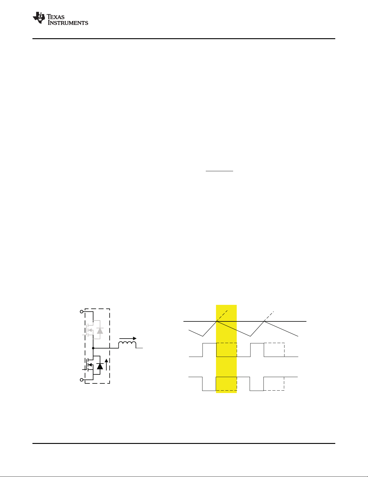
Figure 6 illustrates cycle-by-cycle operation with high It should be noted that a properly functioning
side OC event and Figure 7 shows cycle-by-cycle overcurrent detector assumes the presence of a operation with low side OC. Dashed lines are the proper inductor or power ferrite bead at the operation waveforms when no CBC event is triggered power-stage output. Short-circuit protection is not and solide lines show the waveforms when CBC guaranteed with direct short at the output pins of the event is triggered. In CBC current limiting mode, power stage. when low side FET OC is detected, devcie will turn off the affected low side FET and keep the high side Overtemperature Protection FET at the same half brdige off until next PWM cycle; when high side FET OC is detected, devcie will turn off the affected high side FET and turn on the low side FET at the half brdige until next PWM cycle.
The DRV8312/32 have a two-level
temperature-protection system that asserts an
active-low warning signal (OTW) when the device
junction temperature exceeds 125°C (nominal) and, if
In OC latching shut down mode, the CBC current limit the device junction temperature exceeds 150°C
and error recovery circuitries are disabled and an (nominal), the device is put into thermal shutdown,
overcurrent condition will cause the device to resulting in all half-bridge outputs being set in the
shutdown immediately. After shutdown, RESET_A, high-impedance (Hi-Z) state and FAULT being
RESET_B, and / or RESET_C must be asserted to asserted low. OTSD is latched in this case and
restore normal operation after the overcurrent RESET_A, RESET_B, and RESET_C must be
condition is removed. asserted low to clear the latch.
For added flexibility, the OC threshold is
programmable using a single external resistor
connected between the OC_ADJ pin and AGND pin.
See Table 2 for information on the correlation
between programming-resistor value and the OC
threshold.
Undervoltage Protection (UVP) and Power-On
Reset (POR)
The UVP and POR circuits of the DRV8312/32 fully
protect the device in any power-up / down and
brownout situation. While powering up, the POR
circuit resets the overcurrent circuit and ensures that
Table 2. Programming-Resistor Values and OC
all circuits are fully operational when the GVDD_X
Threshold and VDD supply voltages reach 9.8 V (typical).
OC-ADJUST RESISTOR MAXIMUM CURRENT BEFORE
VALUES (kΩ) OC OCCURS (A)
(1)
19
22 11.6
24 10.7
27 9.7
30 8.8
36 7.4
39 6.9
43 6.3
47 5.8
56 4.9
68 4.1
82 3.4
100 2.8
120 2.4
150 1.9
200 1.4
13.2
Although GVDD_X and VDD are independently
monitored, a supply voltage drop below the UVP
threshold on any VDD or GVDD_X pin results in all
half-bridge outputs immediately being set in the
high-impedance (Hi-Z) state and FAULT being
asserted low. The device automatically resumes
operation when all supply voltage on the bootstrap
capacitors have increased above the UVP threshold.
DEVICE RESET
Three reset pins are provided for independent control
of half-bridges A, B, and C. When RESET_X is
asserted low, two power-stage FETs in half-bridges X
are forced into a high-impedance (Hi-Z) state.
A rising-edge transition on reset input allows the
device to resume operation after a shut-down fault.
E.g., when half-bridge X has OC shutdown, a low to
high transition of RESET_X pin will clear the fault and
FAULT pin. When an OTSD occurs, all three
RESET_A, RESET_B, and RESET_C need to have a
low to high transition to clear the fault and reset
(1) Recommended to use in OC Latching Mode Only FAULT signal.
12 Submit Documentation Feedback Copyright © 2010, Texas Instruments Incorporated
Product Folder Link(s): DRV8312 DRV8332
PWM_HS
PWM_LS
Load
Current
CurrentLimit
T_HS
T_OC
PVDD
GND_X
PWM_HS
PWM_LS
Load
T_LS
CBCwithHighSideOC
DuringT_OCPeriod
DRV8312
DRV8332
www.ti.com
SLES256 –MAY 2010
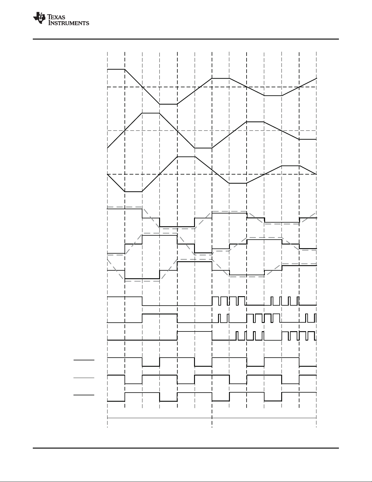
DIFFERENT OPERATIONAL MODES Figure 11 shows six steps trapezoidal scheme with
The DRV8312/32 support two different modes of
operation:
1. Three-phase (3PH) or three half bridges (HB)
with CBC current limit
2. Three-phase or three half bridges with OC
latching shutdown (no CBC current limit)
Because each half bridge has independent supply
and ground pins, a shunt sensing resistor can be
inserted between PVDD to PVDD_X or GND_X to
GND (ground plane). A high side shunt resistor
between PVDD and PVDD_X is recommended for
differential current sensing because a high bias
voltage on the low side sensing could affect device
operation. If low side sensing has to be used, a shunt
resistor value of 10 mΩ or less or sense voltage 100
mV or less is recommended.
Figure 8 and Figure 9 show the three-phase
application examples, and Figure 10 shows how to
connect to DRV8312/32 with some simple logic to
accommodate conventional 6 PWM inputs control.
We recommend using complementary control
scheme for switching phases to prevent circulated
energy flowing inside the phases and to make current
limiting feature active all the time. Complementary
control scheme also forces the current flowing
through sense resistors all the time to have a better
current sensing and control of the system.
hall sensor control and Figure 12 shows six steps
trapezoidal scheme with sensorless control. The hall
sensor sequence in real application might be different
than the one we showed in Figure 11 depending on
the motor used. Please check motor manufacture
datasheet for the right sequence in applications. In
six step trapezoidal complementary control scheme, a
half bridge with larger than 50% duty cycle will have a
positive current and a half bridge with less than 50%
duty cycle will have a negative current. For normal
operation, changing PWM duty cycle from 50% to
100% will adjust the current from 0 to maximum value
with six steps control. It is recommanded to apply a
minimum 50ns to 100 nS PWM pulse at each
switching cycle at lower side to properly charge the
bootstrap cap. The impact of minimum pulse at low
side FET is pretty small, e.g., the maximum duty
cycle is 99.9% with 100ns minimum pulse on low
side. RESET_Xpin can be used to get channel X into
high impedance mode. If you prefer PWM switching
one channel but hold low side FET of the other
channel on (and third channel in Hi-Z) for 2-quadrant
mode, OT latching shutdown mode is recommended
to prevent the channel with low side FET on stuck in
Hi-Z during OC event in CBC mode.
The DRV8312/32 can also be used for sinusoidal
waveform control and field oriented control. Please
check TI website MCU motor control library for
control algorithms.
Figure 6. Cycle-by-Cycle Operation with High Side OC (dashed line: normal operation; solid line: CBC
event)
Copyright © 2010, Texas Instruments Incorporated Submit Documentation Feedback 13
Product Folder Link(s): DRV8312 DRV8332

PWM_HS
PWM_LS
Load
Current
CurrentLimit
CBCwithLowSideOC
T_LS T_OC
PVDD
GND_X
DuringT_OCPeriod
PWM_HS
PWM_LS
Load
T_HS
GVDD
GVDD
PVDD
PVDD
1000 Fm
Loc
Loc
Loc
3.3
10nF
100nF
100nF
100nF
1 Fm
1 Fm
1 Fm
100nF
47 Fm
330 Fm
Roc_adj
Controller
(MSP430
C2000or
StellarisMCU)
RESET_A
PWM_B
OC_ADJ
GND
GND_A
GND_B
OUT_B
PVDD_B
AGND
VREG
M3
M2
BST_B
NC
NC
GND
RESET_C
PWM_C
VDD
GVDD_C
OUT_C
PVDD_C
BST_C
GVDD_C
RESET_B
GND_C
M1
GND
GVDD_B
OTW
FAULT
PWM_A
GVDD_A
BST_A
PVDD_A
OUT_A
100nF
100nF
100nF
M
Rsense_B
Rsense_C
Rsense_A
1
Rsense_x
or
Vsense<100mV
£ 10mW
DRV8332
1 Fm
DRV8312
DRV8332
SLES256 –MAY 2010
www.ti.com
Figure 7. Cycle-by-Cycle Operation with Low Side OC (dashed line: normal operation; solid line: CBC
event)
14 Submit Documentation Feedback Copyright © 2010, Texas Instruments Incorporated
Figure 8. DRV8332 Application Diagram for Three-Phase Operation
Product Folder Link(s): DRV8312 DRV8332

OTW
BST_A
GVDD
GVDD
PVDD
PVDD
1000 Fm
Loc
Loc
Loc
3.3
10nF
100nF
100nF
100nF
1 Fm
1 Fm
1 Fm
47 Fm
330 Fm
Controller
(MSP430
C2000or
StellarisMCU)
RESET_A
PWM_B
OC_ADJ
GND
GND_A
GND_B
OUT_B
PVDD_B
AGND
VREG
M3
M2
BST_B
NC
NC
GND
RESET_C
PWM_C
NC
NC
OUT_C
PVDD_C
PVDD_C
NC
RESET_B
GND_C
M1 GND
NC
NC
FAULT
PWM_A
NC
PVDD_A
PVDD_A
OUT_A
100nF
100nF
100nF
M
Rsense_B
Rsense_C
Rsense_A
Rsense_x
or
Vsense<100mV
£ 10mW
GVDD_B
GVDD_A
VDD
BST_C
GVDD_C
GVDD_C
DRV8312
100nF
Roc_adj
1
1 Fm
PVDD
OUT_A
PWM_A
PWM_B
OUT_C
RESET_A
GND_A
MOTOR
PWM_C
GND_B
GND_C
RESET_C
RESET_B
PWM_AH
PWM_CH
PWM_BH
PWM_AL
PWM_CL
PWM_BL
Controller
OUT_B
DRV8312
DRV8332
www.ti.com
SLES256 –MAY 2010
Figure 9. DRV8312 Application Diagram for Three-Phase Operation
Copyright © 2010, Texas Instruments Incorporated Submit Documentation Feedback 15
Figure 10. Control Signal Logic with Conventional 6 PWM Input Scheme
Product Folder Link(s): DRV8312 DRV8332

PWM_A
PWM_B
PWM_C
PhaseCurrent A
PhaseCurrentB
PhaseCurrentC
HallSensorH1
HallSensorH2
HallSensorH3
S1 S6S5S4S3S2 S1 S6S5S4S3S2
PWM=100% PWM=75%
360
o
360
o
RESET_A
RESET_B
RESET_C
DRV8312
DRV8332
SLES256 –MAY 2010
www.ti.com
Figure 11. Hall Sensor Control with 6 Steps Trapezoidal Scheme
16 Submit Documentation Feedback Copyright © 2010, Texas Instruments Incorporated
Product Folder Link(s): DRV8312 DRV8332
PWM_A
PWM_B
PWM_C
Phase A
CurrentandVoltage
PhaseB
CurrentandVoltage
PhaseC
CurrentandVoltage
BackEMF(Vab)
Ia
Ib
Ic
Va
Vb
Vc
PWM=100% PWM=75%
S1 S6S5S4S3S2 S1 S6S5S4S3S2
BackEMF(Vbc)
BackEMF(Vca)
360
o
360
o
0V
0V
0V
0A
0A
0A
0V
0V
0V
RESET_A
RESET_B
RESET_C
DRV8312
DRV8332
www.ti.com
SLES256 –MAY 2010
Copyright © 2010, Texas Instruments Incorporated Submit Documentation Feedback 17
Figure 12. Sensorless Control with 6 Steps Trapezoidal Scheme
Product Folder Link(s): DRV8312 DRV8332

DRV8312
DRV8332
SLES256 –MAY 2010
www.ti.com
APPLICATION INFORMATION
SYSTEM DESIGN RECOMMENDATIONS
Voltage of Decoupling Capacitor
The voltage of the decoupling capacitors should be selected in accordance with good design practices.
Temperature, ripple current, and voltage overshoot must be considered. The high frequency decoupling capacitor
should use ceramic capacitor with X5R or better rating. For a 50-V application, a minimum voltage rating of 63 V
is recommended.
Current Requirement of 12V Power Supply
The DRV8312/32 require a 12V power supply for GVDD and VDD pins. The total supply current is pretty low at
room temp (less than 50mA), but the current could increase significantly when the device temperature goes too
high (e.g. above 125°C), especially at heave load conditions due to substrate current collection by 12V guard
rings. So it is recommended to design the 12V power supply with current capability at least 5-10% of your load
current and no less than 100mA to assure the device performance across all temperature range.
VREG Pin
The VREG pin is used for internal logic and should not be used as a voltage source for external circuitries. The
capacitor on VREG pin should be connected to AGND.
VDD Pin
The transient current in VDD pin could be significantly higher than average current through VDD pin. A low
resistive path to GVDD should be used. A 22-µF to 47-µF capacitor should be placed on VDD pin beside the
100-nF to 1-µF decoupling capacitor to provide a constant voltage during transient.
OTW Pin
OTW reporting indicates the device approaching high junction temperature. This signal can be used with MCU to
decrease system power when OTW is low in order to prevent OT shut down at a higher temperature.
No external pull up resistor or 3.3V power supply is needed for 3.3V logic. The OTW pin has an internal pullup
resistor connecting to an internal 3.3V to reduce external component count. For 5V logic, an external pull up
resistor to 5V is needed.
FAULT Pin
The FAULT pin reports any fault condition resulting in device shut down. No external pull up resistor or 3.3V
power supply is needed for 3.3V logic. The FAULT pin has an internal pullup resistor connecting to an internal
3.3V to reduce external component count. For 5V logic, an external pull upresistor to 5V is needed.
OC_ADJ Pin
For accurate control of the oevercurrent protection, the OC_ADJ pin has to be connected to AGND through an
OC adjust resistor.
PWM_X and RESET_X Pins
It is recommanded to connect these pins to either AGND or GND when they are not used, and these pins only
support 3.3V logic.
Mode Select Pins
Mode select pins (M1, M2, and M3) should be connected to either VREG (for logic high) or AGND for logic low. It
is not recommended to connect mode pins to board ground if 1-Ω resistor is used between AGND and GND.
18 Submit Documentation Feedback Copyright © 2010, Texas Instruments Incorporated
Product Folder Link(s): DRV8312 DRV8332

_
_ min
PVDD Toc delay
Loc
Ipeak Iave
×
=
-
DRV8312
DRV8332
www.ti.com
SLES256 –MAY 2010
Output Inductor Selection
For normal operation, inductance in motor (assume larger than 10 µH) is sufficient to provide low di/dt output
(e.g. for EMI) and proper protection during overload condition (CBC current limiting feature). So no additional
output inductors are needed during normal operation.
However during a short condition, the motor (or other load) could be shorted, so the load inductance might not
present in the system anymore; the current in short condition can reach such a high level that may exceed the
abs max current rating due to extremely low impendence in the short circuit path and high di/dt before oc
detection circuit kicks in. So a ferrite bead or inductor is recommended to utilize the short circuit protection
feature in DRV8312/32. With an external inductor or ferrite bead, the current will rise at a much slower rate and
reach a lower current level before oc protection starts. The device will then either operate CBC current limit or
OC shut down automatically (when current is well above the current limit threshold) to protect the system.
For a system that has limited space, a power ferrite bead can be used instead of an inductor. The current rating
of ferrite bead has to be higher than the RMS current of the system at normal operation. A ferrite bead designed
for very high frequency is NOT recommended. A minimum impedance of 10 Ω or higher is recommended at 10
MHz or lower frequency to effectively limit the current rising rate during short circuit condition.
The TDK MPZ2012S300A and MPZ2012S101A (with size of 0805 inch type) have been tested in our system to
meet short circuit conditions in the DRV8312. But other ferrite beads that have similar frequency characteristics
can be used as well.
For higher power applications, such as in the DRV8332, there might be limited options to select suitable ferrite
bead with high current rating. If an adequate ferrite bead cannot be found, an inductor can be used.
The inductance can be calculated as:
(1)
Where Toc_delay = 250 nS, Ipeak = 15 A (below abs max rating).
Because an inductor usually saturates pretty quickly after reaching its current rating, it is recommended to use an
inductor with a doubled value or an inductor with a current rating well above the operating condition.
PCB LAYOUT RECOMMENDATION
PCB Material Recommendation
FR-4 Glass Epoxy material with 2 oz. copper on both top and bottom layer is recommended for improved thermal
performance (better heat sinking) and less noise susceptibility (lower PCB trace inductance).
Ground Plane
Because of the power level of these devices, it is recommended to use a big unbroken single ground plane for
the whole system / board. The ground plane can be easily made at bottom PCB layer. In order to minimize the
impedance and inductance of ground traces, the traces from ground pins should keep as short and wide as
possible before connected to bottom ground plane through vias. Multiple vias are suggested to reduce the
impedance of vias. Try to clear the space around the device as much as possible especially at bottom PCB side
to improve the heat spreading.
Decoupling Capacitor
High frequency decoupling capacitors (100 nF) should be placed close to PVDD_X pins and with a short ground
return path to minimize the inductance on the PCB trace.
AGND
AGND is a localized internal ground for logic signals. A 1-Ω resistor is recommended to be connected between
GND and AGND to isolate the noise from board ground to AGND. There are other two components are
connected to this local ground: 0.1-µF capacitor between VREG to AGND and Roc_adj resistor between
OC_ADJ and AGND. Capacitor for VREG should be placed close to VREG and AGND pins and connected
without vias.
Copyright © 2010, Texas Instruments Incorporated Submit Documentation Feedback 19
Product Folder Link(s): DRV8312 DRV8332

DRV8312
DRV8332
SLES256 –MAY 2010
www.ti.com
Current Shunt Resistor
If current shunt resistor is connected between GND_X to GND or PVDD_X to PVDD, make sure there is only one
single path to connect each GND_X or PVDD_X pin to shunt resistor, and the path is short and symmetrical on
each sense path to minimize the measurement error due to additional resistance on the trace.
PCB LAYOUT EXAMPLE
An example of the schematic and PCB layout of DRV8312 are shown in Figure 13, Figure 14, and Figure 15.
20 Submit Documentation Feedback Copyright © 2010, Texas Instruments Incorporated
Product Folder Link(s): DRV8312 DRV8332

GND
GND
GND
Orange
Orange
Orange
Orange
Orange
GND
GND
GVDD
GND
GVDD
GVDD
GND
GND
GND
GND
0.1ufd/100V
0805
C37
0.1ufd/100V
0805
C43
0.1ufd/100V
0805
C46
2
3
1
S1
1
3
2
RSTB
47K
0603
R37
0.1ufd/16V
0603
C33
1.0ufd/16V
0603
C35
1.0ufd/16V
0603
C34
1.0ufd/16V
0603
C30
30ohms/6A
0805
L2
30ohms/6A
0805
L3
30ohms/6A
0805
L4
47ufd/16V
M
C31
+
1.0ufd/16V
0603
C32
PVDD
499
0603
R39
1000pfd/100V
0603
C50
GND
GND
PVDD
PVDD
OUTC
OUTB
OUTA
10.0K
0603
R38
499
0603
R43
1000pfd/100V
0603
C56
GND
GND
10.0K
0603
R42
499
0603
R45
1000pfd/100V
0603
C55
10.0K
0603
R44
+3.3V
GND
0.1ufd/16V
0603
C23
33 1/8W
0805
R18
931
0603
R34
931
0603
R35
619
0603
R29
619
0603
R30
931
0603
R33
0.0
0603
R21
0.0
0603
R22
0.0
0603
R23
1.0 1/4W
0805
R36
0.1ufd/100V
0805
C36
0.1ufd/100V
0805
C42
0.1ufd/100V
0805
C45
619
0603
R31
Orange
OUT_C
Orange
OUT_B
Orange
OUT_A
0.01 1W
1206
R50
15.4K
0603
R49
15.4K
0603
R55
15.4K
0603
R54
220pfd/50V
0603
C20
220pfd/50V
0603
C21
220pfd/50V
0603
C22
220pfd/50V
0603
C27
220pfd/50V
0603
C26
220pfd/50V
0603
C28
10.2K
0603
R25
10.2K
0603
R26
10.2K
0603
R27
1000pfd/50V
0603
C60
GND
GND
1000pfd/50V
0603
C59
1000pfd/50V
0603
C58
HTSSOP44-DDW
1
2
3
4
5
6
7
8
9
10
11
12
13
14
15
16
17
18
19
20
21
22 23
24
25
26
27
28
29
30
31
32
33
34
35
36
37
38
39
40
41
42
43
44
DRV8312DDW
U1
HTSSOP44-DDW
U1
PowerPad
GND
619
0603
R28
931
0603
R32
15.4K
0603
R48
220pfd/50V
0603
C19
220pfd/50V
0603
C25
1000pfd/50V
0603
C57
1
2
3
M1
2
3
1
RSTC
0.01 1W
1206
R53
0.01 1W
1206
R52
GND
0.005 1W
1206
R51
10.2K
0603
R24
0.0
0603
R20
30.1K
0603
R41
GND
30.1K
0603
R40
GND
+2.5V
+2.5V
+2.5V
+2.5V
30.1K
0603
R16
GND
30.1K
0603
R62
GND
SOT23-DBV
2
1
5
4
3
OPA365AIDBV
OA1
+IN
-IN
V-
VOUT
V+
GND
OA2
OPA365AIDBV
3
4
5
1
2
SOT23-DBV
+IN
-IN
V-
VOUT
V+
+3.3V
GND
GND
V-
SOT23-DBV
2
1
5
4
3
OPA365AIDBV
OA3
+IN
-IN
VOUT
V+
+3.3V
GND
0.1ufd/16V
0603
C29
33 1/8W
0805
R63
GND
R19
0805
33 1/8W
C24
0603
0.1ufd/16V
OA4
OPA365AIDBV
3
4
5
1
2
SOT23-DBV
V-
+IN
-IN
VOUT
V+
+3.3V
GND
C39
0603
0.1ufd/16V
R64
0805
33 1/8W
GND
STUFF OPTION
STUFF OPTION
ROUTED GROUND
(SHIELDED FROM GND PLANE)
IS-IhbB
IS-IhbA
IS-IhbC
ADC-Vhb2
IS-TOTAL
IS-IhbA IS-IhbB
IS-IhbC
IS-TOTAL
DRV8312
DRV8332
www.ti.com
SLES256 –MAY 2010
Copyright © 2010, Texas Instruments Incorporated Submit Documentation Feedback 21
Figure 13. DRV8312 Schematic Example
Product Folder Link(s): DRV8312 DRV8332

C37
C33
T1
T2
T3
T4
C46
C43
B1
DRV8312
DRV8332
SLES256 –MAY 2010
T1: PVDD decoupling capacitors C37, C43, and C46 should be placed very close to PVDD_X pins and ground return
path.
T2: VREG decoupling capacitor C33 should be placed very close to VREG abd AGND pins.
T3: Clear the space above and below the device as much as possible to improve the thermal spreading.
T4: Add many vias to reduce the impedance of ground path through top to bottom side. Make traces as wide as
possible for ground path such as GND_X path.
www.ti.com
Figure 14. Printed Circuit Board – Top Layer
B1: Do not block the heat transfer path at bottom side. Clear as much space as possible for better heat spreading.
Figure 15. Printed Circuit Board – Bottom Layer
22 Submit Documentation Feedback Copyright © 2010, Texas Instruments Incorporated
Product Folder Link(s): DRV8312 DRV8332

DRV8312
DRV8332
www.ti.com
SLES256 –MAY 2010
THERMAL INFORMATION
The thermally enhanced package provided with the DRV8332 is designed to interface directly to heat sink using
a thermal interface compound in between, (e.g., Ceramique from Arctic Silver, TIMTronics 413, etc.). The heat
sink then absorbs heat from the ICs and couples it to the local air. It is also a good practice to connect the
heatsink to system ground on the PCB board to reduce the ground noise.
R
is a system thermal resistance from junction to ambient air. As such, it is a system parameter with the
qJA
following components:
• R
• Thermal grease thermal resistance
• Heat sink thermal resistance
The thermal grease thermal resistance can be calculated from the exposed power pad or heat slug area and the
thermal grease manufacturer's area thermal resistance (expressed in °C-in2/W or °C-mm2/W). The approximate
exposed heat slug size is as follows:
• DRV8332, 36-pin PSOP3 …… 0.124 in2(80 mm2)
The thermal resistance of a thermal pad is considered higher than a thin thermal grease layer and is not
recommended. Thermal tape has an even higher thermal resistance and should not be used at all. Heat sink
thermal resistance is predicted by the heat sink vendor, modeled using a continuous flow dynamics (CFD) model,
or measured.
Thus the system R
See the TI application report, IC Package Thermal Metrics (SPRA953A), for more thermal information.
(the thermal resistance from junction to case, or in this example the power pad or heat slug)
qJC
qJA
= R
+ thermal grease resistance + heat sink resistance.
qJC
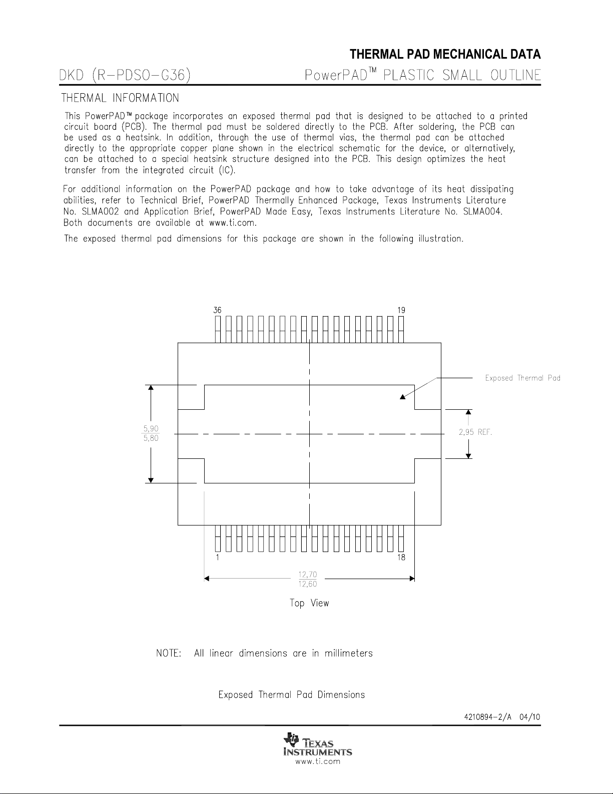
DRV8312 Thermal Via Design Recommendation
Thermal pad of the DRV8312 is attached at bottom of device to improve the thermal capability of the device. The
thermal pad has to be soldered with a very good coverage on PCB in order to deliver the power specified in the
datasheet. The figure below shows the recommended thermal via and land pattern design for the DRV8312. For
additional information, see TI application report, PowerPad Made Easy (SLMA004B) and PowerPad Layout
Guidelines (SOLA120).
Figure 16. DRV8312 Thermal Via Footprint
Copyright © 2010, Texas Instruments Incorporated Submit Documentation Feedback 23
Product Folder Link(s): DRV8312 DRV8332

PACKAGE OPTION ADDENDUM
www.ti.com
3-Jul-2010
PACKAGING INFORMATION
Orderable Device
DRV8312DDW ACTIVE HTSSOP DDW 44 35 Green (RoHS
DRV8312DDWR ACTIVE HTSSOP DDW 44 2000 Green (RoHS
DRV8332DKD ACTIVE HSSOP DKD 36 29 Green (RoHS
DRV8332DKDR ACTIVE HSSOP DKD 36 500 Green (RoHS
(1)
The marketing status values are defined as follows:
ACTIVE: Product device recommended for new designs.
LIFEBUY: TI has announced that the device will be discontinued, and a lifetime-buy period is in effect.
NRND: Not recommended for new designs. Device is in production to support existing customers, but TI does not recommend using this part in a new design.
PREVIEW: Device has been announced but is not in production. Samples may or may not be available.
OBSOLETE: TI has discontinued the production of the device.
Status
(1)
Package Type Package
Drawing
Pins Package Qty
Eco Plan
& no Sb/Br)
& no Sb/Br)
& no Sb/Br)
& no Sb/Br)
(2)
Lead/
Ball Finish
CU NIPDAU Level-3-260C-168 HR Purchase Samples
CU NIPDAU Level-3-260C-168 HR Purchase Samples
NIPDAU Level-4-260C-72 HR Request Free Samples
NIPDAU Level-4-260C-72 HR Purchase Samples
MSL Peak Temp
(3)
Samples
(Requires Login)
(2)
Eco Plan - The planned eco-friendly classification: Pb-Free (RoHS), Pb-Free (RoHS Exempt), or Green (RoHS & no Sb/Br) - please check http://www.ti.com/productcontent for the latest availability
information and additional product content details.
TBD: The Pb-Free/Green conversion plan has not been defined.
Pb-Free (RoHS): TI's terms "Lead-Free" or "Pb-Free" mean semiconductor products that are compatible with the current RoHS requirements for all 6 substances, including the requirement that
lead not exceed 0.1% by weight in homogeneous materials. Where designed to be soldered at high temperatures, TI Pb-Free products are suitable for use in specified lead-free processes.
Pb-Free (RoHS Exempt): This component has a RoHS exemption for either 1) lead-based flip-chip solder bumps used between the die and package, or 2) lead-based die adhesive used between
the die and leadframe. The component is otherwise considered Pb-Free (RoHS compatible) as defined above.
Green (RoHS & no Sb/Br): TI defines "Green" to mean Pb-Free (RoHS compatible), and free of Bromine (Br) and Antimony (Sb) based flame retardants (Br or Sb do not exceed 0.1% by weight
in homogeneous material)
(3)
MSL, Peak Temp. -- The Moisture Sensitivity Level rating according to the JEDEC industry standard classifications, and peak solder temperature.
Important Information and Disclaimer:The information provided on this page represents TI's knowledge and belief as of the date that it is provided. TI bases its knowledge and belief on information
provided by third parties, and makes no representation or warranty as to the accuracy of such information. Efforts are underway to better integrate information from third parties. TI has taken and
continues to take reasonable steps to provide representative and accurate information but may not have conducted destructive testing or chemical analysis on incoming materials and chemicals.
TI and TI suppliers consider certain information to be proprietary, and thus CAS numbers and other limited information may not be available for release.
In no event shall TI's liability arising out of such information exceed the total purchase price of the TI part(s) at issue in this document sold by TI to Customer on an annual basis.
Addendum-Page 1

PACKAGE MATERIALS INFORMATION
www.ti.com 20-Jul-2010
TAPE AND REEL INFORMATION
*All dimensions are nominal
Device Package
DRV8312DDWR HTSSOP DDW 44 2000 330.0 24.4 8.6 15.6 1.8 12.0 24.0 Q1
DRV8332DKDR HSSOP DKD 36 500 330.0 24.4 14.7 16.4 4.0 20.0 24.0 Q1
Type
Package
Drawing
Pins SPQ Reel
Diameter
(mm)
Reel
Width
W1 (mm)
A0
(mm)B0(mm)K0(mm)P1(mm)W(mm)
Pin1
Quadrant
Pack Materials-Page 1

PACKAGE MATERIALS INFORMATION
www.ti.com 20-Jul-2010
*All dimensions are nominal
Device Package Type Package Drawing Pins SPQ Length (mm) Width (mm) Height (mm)
DRV8312DDWR HTSSOP DDW 44 2000 346.0 346.0 41.0
DRV8332DKDR HSSOP DKD 36 500 346.0 346.0 41.0
Pack Materials-Page 2


IMPORTANT NOTICE
Texas Instruments Incorporated and its subsidiaries (TI) reserve the right to make corrections, modifications, enhancements, improvements,
and other changes to its products and services at any time and to discontinue any product or service without notice. Customers should
obtain the latest relevant information before placing orders and should verify that such information is current and complete. All products are
sold subject to TI’s terms and conditions of sale supplied at the time of order acknowledgment.
TI warrants performance of its hardware products to the specifications applicable at the time of sale in accordance with TI’s standard
warranty. Testing and other quality control techniques are used to the extent TI deems necessary to support this warranty. Except where
mandated by government requirements, testing of all parameters of each product is not necessarily performed.
TI assumes no liability for applications assistance or customer product design. Customers are responsible for their products and
applications using TI components. To minimize the risks associated with customer products and applications, customers should provide
adequate design and operating safeguards.
TI does not warrant or represent that any license, either express or implied, is granted under any TI patent right, copyright, mask work right,
or other TI intellectual property right relating to any combination, machine, or process in which TI products or services are used. Information
published by TI regarding third-party products or services does not constitute a license from TI to use such products or services or a
warranty or endorsement thereof. Use of such information may require a license from a third party under the patents or other intellectual
property of the third party, or a license from TI under the patents or other intellectual property of TI.
Reproduction of TI information in TI data books or data sheets is permissible only if reproduction is without alteration and is accompanied
by all associated warranties, conditions, limitations, and notices. Reproduction of this information with alteration is an unfair and deceptive
business practice. TI is not responsible or liable for such altered documentation. Information of third parties may be subject to additional
restrictions.
Resale of TI products or services with statements different from or beyond the parameters stated by TI for that product or service voids all
express and any implied warranties for the associated TI product or service and is an unfair and deceptive business practice. TI is not
responsible or liable for any such statements.
TI products are not authorized for use in safety-critical applications (such as life support) where a failure of the TI product would reasonably
be expected to cause severe personal injury or death, unless officers of the parties have executed an agreement specifically governing
such use. Buyers represent that they have all necessary expertise in the safety and regulatory ramifications of their applications, and
acknowledge and agree that they are solely responsible for all legal, regulatory and safety-related requirements concerning their products
and any use of TI products in such safety-critical applications, notwithstanding any applications-related information or support that may be
provided by TI. Further, Buyers must fully indemnify TI and its representatives against any damages arising out of the use of TI products in
such safety-critical applications.
TI products are neither designed nor intended for use in military/aerospace applications or environments unless the TI products are
specifically designated by TI as military-grade or "enhanced plastic." Only products designated by TI as military-grade meet military
specifications. Buyers acknowledge and agree that any such use of TI products which TI has not designated as military-grade is solely at
the Buyer's risk, and that they are solely responsible for compliance with all legal and regulatory requirements in connection with such use.
TI products are neither designed nor intended for use in automotive applications or environments unless the specific TI products are
designated by TI as compliant with ISO/TS 16949 requirements. Buyers acknowledge and agree that, if they use any non-designated
products in automotive applications, TI will not be responsible for any failure to meet such requirements.
Following are URLs where you can obtain information on other Texas Instruments products and application solutions:
Products Applications
Amplifiers amplifier.ti.com Audio www.ti.com/audio
Data Converters dataconverter.ti.com Automotive www.ti.com/automotive
DLP® Products www.dlp.com Communications and www.ti.com/communications
DSP dsp.ti.com Computers and www.ti.com/computers
Clocks and Timers www.ti.com/clocks Consumer Electronics www.ti.com/consumer-apps
Interface interface.ti.com Energy www.ti.com/energy
Logic logic.ti.com Industrial www.ti.com/industrial
Power Mgmt power.ti.com Medical www.ti.com/medical
Microcontrollers microcontroller.ti.com Security www.ti.com/security
RFID www.ti-rfid.com Space, Avionics & www.ti.com/space-avionics-defense
RF/IF and ZigBee® Solutions www.ti.com/lprf Video and Imaging www.ti.com/video
Mailing Address: Texas Instruments, Post Office Box 655303, Dallas, Texas 75265
Copyright © 2010, Texas Instruments Incorporated
Telecom
Peripherals
Defense
Wireless www.ti.com/wireless-apps
 Loading...