


 Loading...
KE-32TS2U/32TS2E
PANEL MODULE SERVICE MANUAL
UC Model
AEP Model
PDP Module Name
FPF32C106128UA-7X
UK Model
Koria Model
FLAT PANEL COLOR TV
|
Contents |
|
1. Outline |
|
|
1.1 |
Out view ------------------------------------------------------------------------------ |
1 |
1.2 |
Feature -------------------------------------------------------------------------------- |
2 |
1.3 |
Specification |
|
1.3.1 Functional specification ------------------------------------------------------ |
2 |
|
1.3.2 Display quality specification ------------------------------------------------- |
3 |
|
1.3.3 I/O Interface specification ---------------------------------------------------- |
4 |
|
2. Notes on safe handling of the plasma display |
|
|
2.1 |
Notes to follow during servicing ------------------------------------------------- |
10 |
3. Name and Function |
|
|
3.1 |
Configuration ----------------------------------------------------------------------- |
11 |
3.2 |
Block Diagrams |
|
3.2.1 Signal Diagrams -------------------------------------------------------------- |
12 |
|
3.2.2 Power Diagrams -------------------------------------------------------------- |
13 |
|
3.3 |
Function ----------------------------------------------------------------------------- |
14 |
3.3.1 Function of LOGIC CIRCUIT BOARD ---------------------------------- |
14 |
|
3.3.2 Function of X-SUS CIRCUIT BOARD ---------------------------------- |
22 |
|
3.3.3 Function of Y-SUS CIRCUIT BOARD ---------------------------------- |
22 |
|
3.3.4 Function of PSU CIRCUIT BOARD ------------------------------------- |
22 |
|
3.4 |
Protection function ---------------------------------------------------------------- |
23 |
4. Problem analysis |
|
|
4.1 |
Outline of Repair Flow ---------------------------------------------------------- |
24 |
4.2 |
Outline of PDP Module Repair Flow ------------------------------------------ |
25 |
4.3 |
Checking the Product Requested for Repair ---------------------------------- |
28 |
4.4 |
Operation Test Procedure -------------------------------------------------------- |
29 |
4.5 |
Fault Symptom -------------------------------------------------------------------- |
30 |
4.6 |
Failure analysis procedure |
|
4.6.1 Procedure of no screen (Power supply) ----------------------------------- |
33 |
|
4.6.2 Vertical line/Vertical bar analysis procedure ----------------------------- |
40 |
|
4.6.3 Horizontal line/Horizontal bar --------------------------------------------- |
44 |
|
4.7 Failure Analysis using a personal computer |
|
|
4.7.1 Connection a Computer ----------------------------------------------------- |
45 |
|
4.7.2 Preparing a Computer ------------------------------------------------------- |
45 |
|
4.7.3 Problem Analysis procedure ----------------------------------------------- |
46 |
5. DISASSEMBLE AND REASSEMBLING |
|
5.1 Disassembling overview --------------------------------------------------------- |
50 |
5.2 X-SUS CIRCUIT BOARD REMOVING MANUAL ----------------------- |
51 |
5.3 Y-SUS CIRCUIT BOARD REMOVING MANUAL ----------------------- |
53 |
5.4 ADDRESS-BUS Left CIRCUIT BOARD REMOVING MANUAL ----- |
55 |
5.5 ADDRESS-BUS Right CIRCUIT BOARD REMOVING MANUAL ---- |
57 |
5.6 LOGIC CIRCUIT BOARD REMOVING MANUAL ----------------------- |
59 |
5.7 PSU CIRCUIT BOARD REMOVING MANUAL --------------------------- |
61 |
5.8 Panel chassis Replacement procedure ------------------------------------------ |
64 |
6. Checking and adjustment |
|
6.1 Check and Adjustment list ------------------------------------------------------- |
65 |
6.2 Check and Adjustment ------------------------------------------------------------ |
66 |
6.2.1 Check and Adjustment Procedure ----------------------------------------- |
66 |
6.2.2 Glass panel driving voltage adjustment ----------------------------------- |
67 |
6.2.3 Operation performance check ---------------------------------------------- |
69 |
6.2.4 Heat-running test ------------------------------------------------------------- |
71 |
6.2.5 Logic board parameter forwarding ----------------------------------------- |
72 |
6.2.6 Accumulation time reset ----------------------------------------------------- |
73 |
6.2.7 Setup before shipment ------------------------------------------------------- |
74 |
7. The parts Information --------------------------------------------------------- |
75 |
1.Out line
The module is a plasma display module which can be designed in there is no fan in addition to a general feature of the plasma display such as a flat type, lightness, and high-viewing-angle and terrestrial magnetism.
1.1Out view
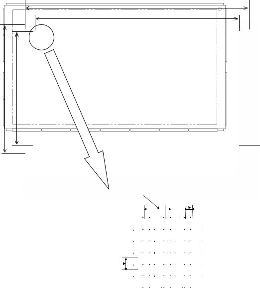
784
715.68
448 |
399.36 |
Pixel pitch(horizontal) |
|
|
|
|
|
|
|
|
|
Subpixel pitch(horizontal) |
||||||||
|
0.84mm |
|
|
|
|
|
|
|
|
|
|
0.28mm |
||||||
|
|
|
|
|
|
|
|
|
|
|
|
|
|
|
|
|
|
|
|
|
R |
|
G |
|
B |
R |
|
G |
|
B |
R |
|
G |
|
B |
|
|
|
|
|
|
|
|
|
|
|
|
|
|
|
|
|
|
|
|
|
|
|
R |
|
G |
|
B |
R |
|
G |
|
B |
R |
|
G |
|
B |
|
|
|
|
|
|
|
|
|
|
|
|
|
|
|
|
|
|
|
|
|
Pixelpitch(Vertical) |
|
R |
|
G |
|
B |
R |
|
G |
|
B |
R |
|
G |
|
B |
|
|
|
|
|
|
|
|
|
|
|
|
|
|
|
|
|
|
|
|
|
mm0.39 |
R |
|
G |
|
B |
R |
|
G |
|
B |
R |
|
G |
|
B |
|
|
|
|
|
|
|
|
|
|
|
|
|
|||||||||
|
|
|
|
|
|
|
|
|
|
|
|
|
|
|
|
|
|
|
|
|
R |
|
G |
|
B |
R |
|
G |
|
B |
R |
|
G |
|
B |
|
|
|
|
|
|
|
|
|
|
|
|
|
|
|
|
|
|
|
|
|
|
|
R |
|
G |
|
B |
R |
|
G |
|
B |
R |
|
G |
|
B |
|
|
|
|
|
|
|
|
|
|
|
|
|
|
|
|
|
|
|
|
|
-1-
1.2Feature
1.For high definition television by ALIS method
2.For FAN Less design(Low consumption electric power)
3.Thin Depth and Lightness
4.Customizing of module equipped with communication function
1.3Specification
1.3.1 Functional specification
|
Item |
NO |
|
Specification |
|
|
|
UA-1x |
|
UA-6x |
7x |
||
|
|
|
|
|||
Externals |
Module size |
1 |
784 x 448 x 65.5 mm |
|
← |
← |
|
Weight |
2 |
13 kg |
|
← |
← |
Display panel |
Display size |
3 |
715.68 x 399.36 mm |
|
← |
← |
|
|
|
(32inch: 16:9) |
|
|
|
|
Aspect ratio |
4 |
16:9 |
|
← |
← |
|
Resolution |
5 |
852 x 1024 pixel |
|
← |
← |
|
Pixel pitch |
6 |
0.84(H) x 0.39(V) mm |
|
← |
← |
|
Sub pixel pitch |
7 |
0.28(H) x 0.39(V) mm |
|
← |
← |
|
|
|
|
|
|
|
Color |
Grayscale (standard) |
8 |
RGB each color |
|
← |
← |
|
|
|
256 Grayscale |
|
|
|
BrightNess |
White (display load |
9 |
650 cd/ (TYP.) |
|
← |
900cd/ |
|
Ratio 1%, standard) |
|
|
|
(typ.) |
|
Chromaticity |
(x,y), white 10% |
10 |
(0.300, 0.290) (TYP.) |
|
← |
(0.300,0.300) |
Coordinates |
|
|
|
|
(typ.) |
|
Contrast |
Contrast in Darkroom (60Hz) |
11 |
500:1 (TYP.) |
|
← |
900:1 |
|
|
|
|
|
(typ.) |
|
|
|
|
|
|
|
|
Data signal |
Video signal |
12 |
LVDS (8bit) |
|
← |
← |
|
(RGB each color) |
|
|
|
|
|
|
Dot clock (max) |
13 |
52 MHz |
|
← |
← |
|
|
|
|
|
|
|
|
|
|
|
|
|
|
Sync Signal |
Horizontal Sync Signal (max) |
14 |
50KHz (LVDS) |
|
← |
← |
|
|
|
|
|
|
|
|
|
|
|
|
|
|
|
Vertical Sync Signal |
15 |
50Hz ± 19/60 ± 1.7Hz |
|
← |
50Hz±1.9 60± |
|
|
|
(LVDS) |
|
1.7 |
|
|
|
|
|
|
|
/70Hz±1.5Hz |
|
|
|
|
|
|
(LVDS) |
Powersupply |
Input voltage/current |
16 |
100-120/200-240VAC |
|
+3.3/+5/+70-90/+ |
+3.3/+5/+70-90/ |
|
|
|
4.0-1.7A 50/60Hz |
|
30-70VDC |
+30-65VDC |
|
|
|
|
|
0.05/6/ 2.5 /2A |
0.05/6/ 2.5 /2A |
|
Standby electric power (max) |
17 |
1W |
|
← |
← |
Noise |
Shade noise at 18dB(A) or less |
18 |
25dB(A) orless |
|
← |
← |
Guarantee |
Temperature (operation) |
19 |
0 - 55°C |
|
← |
← |
environment |
Temperature (storage) |
20 |
0 - 55°C |
|
← |
← |
|
Humidity (operation) |
21 |
20 - 85%RH (no condensation) |
|
← |
← |
|
Humidity (storage) |
22 |
20 - 80%RH (no condensation) |
|
← |
← |
It is made to give priority when there is a delivery specification according to the customer.
-2-
1.3.2 Display quality specification
|
Item |
NO |
|
Specification |
|
|
|
|
|
UA-1x |
|
UA-6x |
UA-7x |
||
|
|
|
|
|
|||
|
|
|
|
|
|
|
|
Non-lighting |
Total number (subpixel) |
1 |
15 or less |
|
|
← |
← |
cell defect |
Density (subpixel/cm2) |
2 |
2 or less |
|
|
← |
← |
|
|
|
(However,1 continuousness or less) |
|
|
|
|
|
Size(HxV) (subpixel) |
3 |
1x2 or less, |
|
|
← |
← |
|
|
|
Or 2x1 or less |
|
|
|
|
Non-extinguish |
Total number (subpixel) |
4 |
6 or less |
|
|
← |
← |
ing cell defect |
|
|
(each color 2 or less) |
|
|
|
|
|
Density (subpixel/ cm2) |
5 |
Each color |
2 cells max |
|
← |
← |
|
|
|
(However,1 continuousness or less) |
|
|
|
|
Flickering cell |
Flickering lighting cell defect |
6 |
5 or less |
|
|
← |
← |
defect |
(sub pixel/ cm2) |
|
|
|
|
|
|
|
Flickering non-extinguishing cell |
7 |
Number on inside of |
|
← |
← |
|
|
defect |
|
Non-extinguishing cell defect |
|
|
|
|
High intensity |
Twice or more bright point |
8 |
0 |
|
|
← |
← |
cell defect |
|
|
|
|
|
|
|
Brightness |
White block of 10% load |
9 |
20 or less |
|
|
← |
← |
variation |
[9 point](%) |
|
|
|
|
|
|
|
In area adjacent 20mm |
10 |
10 or less |
|
|
← |
← |
|
[White](%) |
|
|
|
|
|
|
Color variation |
White block of 10% load |
11 |
X: Average ±0.015 |
|
← |
← |
|
|
[9 point] |
|
y: Average |
±0.015 |
|
|
|
Note: It is made to give priority when there is a delivery specification according to the customer.
-3-
1.3.3I/0 Interface Specification
(1)I/O signal
|
No. |
|
|
Item |
|
|
Signal Name |
|
Number |
|
|
|
Form |
|
|
Content of definition |
|
||
|
|
|
|
|
|
of |
|
I/O |
|
|
|
|
|||||||
|
|
|
|
|
|
|
|
|
|
signals |
|
|
|
|
|
|
|
|
|
|
|
|
|
|
|
|
|
|
|
|
|
|
|
|
|
|
|
||
|
|
|
|
|
|
|
|
RXIN0- |
1 |
|
|
|
|
|
|
|
Differential serial data signal. |
||
|
|
|
|
|
|
|
|
RXIN0+ |
1 |
|
|
|
|
|
|
|
Input video and timing signals |
||
|
|
|
|
|
|
|
Reflection |
RXIN1- |
1 |
|
|
|
LVDS |
|
after differential serial |
||||
|
|
|
|
|
|
|
signal |
RXIN1+ |
1 |
|
|
|
|
conversion using a dedicated |
|||||
|
|
|
|
|
|
|
|
Input |
|
Differe |
|
||||||||
|
|
|
|
|
|
|
Timing |
RXIN2- |
1 |
|
|
|
transceiver. |
||||||
|
|
|
|
|
|
|
|
|
|
ntial |
|
||||||||
|
|
|
|
|
|
|
Signal |
RXIN2+ |
1 |
|
|
|
|
The serial data signal is |
|||||
|
|
|
|
|
|
|
|
|
|
|
|
|
|
||||||
|
|
|
|
|
|
|
|
RXIN3- |
1 |
|
|
|
|
|
|
|
|||
|
|
|
|
|
|
|
|
|
|
|
|
|
|
|
transmitted seven times faster |
||||
|
|
|
|
|
|
|
|
RXIN3+ |
1 |
|
|
|
|
|
|
|
|||
|
|
|
|
|
|
|
|
|
|
|
|
|
|
|
than the base signal. |
||||
|
|
|
|
|
|
|
|
|
|
|
|
|
|
|
|
|
|
||
1 |
|
|
Display |
|
|
|
|
|
|
|
|
|
|
|
|
Differential clock signal. |
|||
|
|
|
|
|
|
|
|
|
|
|
|
|
|
Input the clock signal after |
|||||
|
|
Data |
|
|
|
|
|
|
|
|
LVDS |
|
|||||||
|
|
|
|
|
|
|
|
RXCLKIN- |
1 |
|
|
|
|
differential conversion using a |
|||||
|
|
|
|
|
|
|
Clock |
|
Input |
|
Differe |
|
dedicated transceiver. |
||||||
|
|
|
|
|
|
|
RXCLKIN+ |
1 |
|
|
|
||||||||
|
|
|
|
|
|
|
|
|
|
|
ntial |
|
The clock signal is transmitted |
||||||
|
|
|
|
|
|
|
|
|
|
|
|
|
|
|
|||||
|
|
|
|
|
|
|
|
|
|
|
|
|
|
|
|
|
|
||
|
|
|
|
|
|
|
|
|
|
|
|
|
|
|
|
|
|
at the same speed as the base |
|
|
|
|
|
|
|
|
|
|
|
|
|
|
|
|
|
|
|
signal. |
|
|
|
|
|
|
|
|
|
|
|
|
|
|
|
|
|
|
|
Low: LVDS receiver |
|
|
|
|
|
|
|
|
Power down |
PDWN |
1 |
Input |
|
LVTTL |
|
outputs are all L. |
|||||
|
|
|
|
|
|
|
Signal |
|
|
High: Input signals are |
|||||||||
|
|
|
|
|
|
|
|
|
|
|
|
|
|
|
|
|
|||
|
|
|
|
|
|
|
|
|
|
|
|
|
|
|
|
|
|
||
|
|
|
|
|
|
|
|
|
|
|
|
|
|
|
|
|
|
active. |
|
|
|
|
|
|
|
|
|
SDA |
1 |
|
I/O |
|
|
|
|
|
I2C bus serial data |
||
|
|
|
|
|
|
|
|
|
|
|
|
|
|
communication signal. |
|||||
|
|
|
|
|
|
|
Communication |
|
|
|
|
|
|
LVTTL |
|
||||
|
|
|
|
|
|
|
|
|
|
|
|
2 |
C) |
|
Communication with the |
||||
|
|
|
|
|
|
|
|
SCL |
1 |
|
I/O |
|
(I |
|
control MPU of this product is |
||||
|
|
|
|
|
|
|
|
|
|
|
|
|
|
||||||
|
|
|
|
|
|
|
|
|
|
|
|
|
|
|
|
|
|
enabled. |
|
|
|
|
|
MPU |
|
|
|
|
|
|
|
|
|
|
|
|
Low power consumption mode |
||
|
|
|
|
|
|
CPUGO |
1 |
Input |
|
LVTTL |
|
of the control MPU of this |
|||||||
2 |
|
|
Comm |
|
|
|
|
||||||||||||
|
|
|
|
|
|
|
|
|
|
|
|
|
|
product is released. |
|||||
|
|
unicati |
|
|
|
|
|
|
|
|
|
|
|
|
|||||
|
|
|
|
|
|
|
|
|
|
|
|
|
|
|
|
||||
|
|
|
|
|
|
|
|
|
|
|
|
|
|
|
|
“High”: |
|||
|
|
|
|
on/ |
|
|
|
|
|
|
|
|
|
|
|
|
|||
|
|
|
|
Control |
|
Control |
PDPGO |
1 |
Input |
LVTTL |
|
This product is started. |
|||||||
|
|
|
|
|
|
|
|
|
|
|
|
|
|
|
|
|
(CPUGO=“High” Effective) |
||
|
|
|
|
|
|
|
|
|
|
|
|
|
|
|
|
|
|
It changes into "Low" Î "High" |
|
|
|
|
|
|
|
|
|
|
|
|
|
|
|
|
|
|
|
when this product enters the |
|
|
|
|
|
|
|
|
|
IRQ |
1 |
|
Output |
|
LVTTL |
|
undermentioned state. |
||||
|
|
|
|
|
|
|
|
|
|
|
|
|
|
|
|
|
|
1.Vcc/Va/Vs output decrease |
|
|
|
|
|
|
|
|
|
|
|
|
|
|
|
|
|
|
|
2.Circuit abnormality detection |
|
-4-
(2) LVDS Signal Definition and Function
A video signal (display data signal and control signal) is converted from parallel data to serial data with the LVDS transmitter and further converted into four sets of differential signals before input to this product.
These signals are transmitted seven times faster than dot clock signals.
The dot clock signal is converted into one set of differential signals by the transmitter before input to this product. The LVDS signal definition and function are summarized below:
|
Signal name |
|
Symbol |
Number |
|
|
|
Signal definition and function |
|
|
|
|
|
of signals |
|
|
|
|
|
|
|
|
RXIN0- |
1 |
|
|
Display data signal |
||
|
|
|
|
|
|
|
|
||
|
|
|
RXIN0+ |
1 |
|
|
R0,R1,R2,R3,R4,R5,G0 |
||
|
|
|
|
|
|
|
|
||
|
|
|
RXIN1- |
1 |
|
|
Display data signal |
||
|
|
|
|
|
|
|
|
||
|
|
|
RXIN1+ |
1 |
|
|
G1,G2,G3,G4,G5,B0,B1 |
||
|
Video signal |
|
|
|
|
|
|
|
|
|
Timing signal |
|
RXIN2- |
1 |
|
|
Display data signal, Sync Signal, Control signal |
||
|
Transmission line |
|
|
|
|
|
|
||
|
|
RXIN2+ |
1 |
|
|
B2,B3,B4,B5 |
|
||
|
|
|
|
|
|
||||
|
|
|
|
|
|
_____ |
_____ |
_______ |
|
|
|
|
|
|
|
|
Hsync, |
Vsync, |
BLANK |
|
|
|
|
|
|
|
|
||
|
|
|
RXIN3- |
1 |
|
|
Display data signal, Control signal |
||
|
|
|
|
|
|
|
|
||
|
|
|
RXIN3+ |
1 |
|
|
R6,R7,G6,G7,B6,B7,PARITY |
||
|
|
|
|
|
|
|
|
|
|
|
Clock transmission line |
|
RXCLKIN- |
1 |
|
|
Clock signal |
|
|
|
|
|
_____ |
|
|
||||
|
|
|
RXCLKIN+ |
1 |
|
|
|
||
|
|
|
|
|
DCLK |
|
|
||
|
|
|
|
|
|
|
|
|
|
|
|
|
|
|
|
|
|
|
|
-5-

(3)Video Signal Definition and Function
The table below summarizes the definitions and functions of input video signals before
LVDS conversion.
|
|
|
|
|
|
|
Number |
|
|
Input/ |
|
|
|
|
|
Item |
|
|
Signal name |
|
|
of |
|
|
|
|
Signal definition and function |
|
|
|
|
|
|
|
|
|
output |
|
|
|
||||
|
|
|
|
|
|
|
signals |
|
|
|
|
|
|
|
|
|
|
|
|
|
|
|
|
|
|
|
|
|
Original Display signal (before LVDS transmitta nce)
Video signal |
DATA-R |
8 |
|
|
Display data signal |
|||||||||||||||
DATA-G |
8 |
Input |
|
R7/G7/B7 is the highest intensity bit. |
||||||||||||||||
(digital RGB) |
|
|||||||||||||||||||
|
DATA-B |
8 |
|
|
R0/G0/B0 is the lowest intensity bit. |
|||||||||||||||
|
|
|
|
|
|
|
|
|
Display data timing signal: Data are read |
|||||||||||
Data Clock |
|
|
|
|
|
1 |
Input |
|
when |
DCLK |
is low. |
DCLK |
is continuously |
|||||||
DCLK |
||||||||||||||||||||
|
|
|
|
input. |
||||||||||||||||
|
|
|
|
|
|
|
|
|
||||||||||||
|
|
|
|
|
|
|
|
|
|
|
|
|
|
|
|
|
|
|
|
|
Horizontal sync |
_____ |
|
|
|
|
|
Regulates one horizontal line of data: Begins |
|||||||||||||
|
|
|
|
|
|
|
|
|
|
|
|
|
|
|
|
|||||
|
|
1 |
Input |
|
control of the next screen when Hsync is |
|||||||||||||||
signal |
Hsync |
|
||||||||||||||||||
|
|
|
lowered. |
|||||||||||||||||
|
|
|
|
|
|
|
|
|
||||||||||||
|
|
|
|
|
|
|
|
|
Screen starts up control timing signal: Begins |
|||||||||||
Vertical sync |
_____ |
|
|
|
|
|
control of the next screen when |
Vsync |
is |
|||||||||||
|
|
1 |
Input |
|
lowered. |
|||||||||||||||
signal |
Vsync |
|
||||||||||||||||||
|
|
|
Input the same frequency in both |
|||||||||||||||||
|
|
|
|
|
|
|
|
|
||||||||||||
|
|
|
|
|
|
|
|
|
odd-numbered and even-numbered fields. |
|||||||||||
|
|
|
|
|
|
|
|
This signal specifies the display field. |
||||||||||||
|
|
|
|
|
|
|
|
|
H: Odd-numbered field |
|||||||||||
|
|
|
|
|
|
|
|
|
L: Even-numbered field |
|||||||||||
Parity signal |
PARITY |
1 |
Input |
|
Parity signal should be alternated in every |
|||||||||||||||
|
|
|
|
|
|
|
|
|
Vsync |
cycle. This signal is arbitrarily |
||||||||||
|
|
|
|
|
|
|
|
|
reversed internally when there is no reversing |
|||||||||||
|
|
|
|
|
|
|
|
|
signal. |
|||||||||||
|
|
|
|
|
|
|
|
|
Display period timing signal. |
|||||||||||
|
|
|
|
|
|
|
|
|
H indicates the display period and L indicates |
|||||||||||
|
|
|
|
|
|
|
|
|
the non display period. |
|||||||||||
|
|
|
|
|
|
|
|
|
Note: |
|||||||||||
|
|
|
|
|
|
|
|
|
Set this timing properly like followings, as is |
|||||||||||
|
|
|
|
|
|
|
|
|
used internally for signal processing. |
|||||||||||
|
|
|
|
|
|
|
|
|
Set the blanking period so that the number |
|||||||||||
|
|
|
|
|
|
|
|
|
of effective display data items in one |
|||||||||||
Blanking signal |
|
|
BLANK |
1 |
Input |
|
horizontal period is 852. |
|||||||||||||
|
|
|
Set the number of blanking signals in one |
|||||||||||||||||
|
|
|
|
|
|
|
|
|
vertical period to 512, which is one half the |
|||||||||||
|
|
|
|
|
|
|
|
|
number of effective scan lines. |
|||||||||||
|
|
|
|
|
|
|
|
|
If the |
BLANK |
changes when the Vsync |
|||||||||
|
|
|
|
|
|
|
|
|
frequency is switched, the screen display may |
|||||||||||
|
|
|
|
|
|
|
|
|
be disturbed or brightness may change. |
|||||||||||
|
|
|
|
|
|
|
|
|
The screen display is restored to the normal |
|||||||||||
|
|
|
|
|
|
|
|
|
|
|
|
|
|
|
|
|||||
|
|
|
|
|
|
|
|
|
state later when the BLANK length is |
|||||||||||
|
|
|
|
|
|
|
|
|
constant again. |
|||||||||||
-6-
(4) Connector Specifications
The connector specification is shown below.
Please do not connect anything with the terminal NC.
(I) Signal connector CN1: DF13-20DP-1.25 V (tin-plated) (Maker: HIROSE DENKI)
|
Pin No. |
|
|
Signal name |
Pin No. |
|
Signal name |
|
|
||||
|
|
|
|
|
|
|
|
|
|
|
|
|
|
|
1 |
|
|
RXIN0- |
2 |
|
GND |
|
|
||||
|
|
|
|
|
|
|
|
|
|
|
|
|
|
|
3 |
|
|
RXIN0+ |
4 |
|
SCL |
|
|
||||
|
5 |
|
|
RXIN1- |
6 |
|
GND |
|
|
||||
|
|
|
|
|
|
|
|
|
|
|
|
|
|
|
7 |
|
|
RXIN1+ |
8 |
|
SDA |
|
|
||||
|
9 |
|
|
RXIN2- |
10 |
|
GND |
|
|
||||
|
11 |
|
|
RXIN2+ |
12 |
|
CPUGO |
|
|
||||
|
13 |
|
|
RXCLKIN- |
14 |
|
PDPGO |
|
|
||||
|
15 |
|
|
RXCLKIN+ |
16 |
|
IRQ |
|
|
||||
|
|
|
|
|
|
|
|
|
|
|
|
|
|
|
17 |
|
|
RXIN3- |
18 |
|
PDWN |
|
|
||||
|
19 |
|
|
RXIN3+ |
20 |
|
GND |
|
|
||||
|
|
|
|
|
|
|
|
|
|
|
|
||
|
|
[Conforming connector] |
Housing: DF13-20DS-1.25C |
|
|
||||||||
|
|
|
|
|
|
Contact: DF-2630SCF |
|
|
|||||
(II) Power Source Connectors for power supply(jig) |
|
|
|||||||||||
|
(a) Power input connector |
|
(b) Power supply output connector for system |
||||||||||
|
|
CN61: B06P-VH |
|
|
CN62:B03P-VH |
|
|
||||||
|
|
|
(Maker: JST) |
|
|
|
|
(Maker: JST) |
|||||
|
|
Pin No. |
Symbol |
|
|
|
|
Pin No. |
|
Symbol |
|
||
|
|
|
|
|
|
|
|
|
|
||||
|
1 |
|
AC(L) |
|
|
1 |
|
VAUX |
|
||||
|
2 |
|
N.C |
|
|
2 |
|
N.C |
|
||||
|
3 |
|
AC(N) |
|
|
3 |
|
GND |
|
||||
|
4 |
|
N.C |
|
|
|
|
[Conforming connector] |
|||||
|
5 |
|
N.C |
|
|
|
|
Housing: VHR-03N (or M) |
|||||
|
6 |
|
F.G |
|
|
|
|
Contact: SVH-21T-P1.1 |
|||||
[Conforming connector] Housing: VHR-06N (or M) Contact: SVH-21T-P1.1
(c) Power supply output connector for system CN63: B5B-XH-A
(Maker: JST)
Pin No. |
|
Symbol |
1 |
|
Vpr1 |
2 |
|
N.C. |
3 |
|
Vpr2 |
4 |
|
N.C. |
5 |
|
GND |
[Conforming connector] Housing: XHP-5 Contact: SXH-001T-P0.6
-7-
(III) Power Source Connectors |
|
|
|
|
|
|
|
|
|
|
|
|
|
|
|
|
|
|
|||||||
(a)Power supply output |
(b)Power supply output |
|
(c)Power supply output |
|
|
|
|||||||||||||||||||
|
|
|
|
connector for system |
|
|
connector for system |
connector for system |
|||||||||||||||||
|
|
|
CN6: B6B-PH-SM3-TB(JST) |
|
CN23: B10PS-VH(JST) |
|
|
|
CN33: B9PS-VH(JST) |
||||||||||||||||
|
|
|
|
|
|
|
|
|
|
|
|
|
|
|
|
|
|
|
|
|
|
|
|
|
|
|
|
|
|
Pin No. |
Symbol |
|
|
|
Pin No. |
|
|
Symbol |
|
|
|
|
Pin No. |
|
|
Symbol |
|
||||
|
|
|
1 |
|
Vpr2 |
|
|
1 |
|
|
|
Va |
|
|
|
1 |
|
|
Vcc |
|
|||||
|
|
|
2 |
|
N.C. |
|
|
2 |
|
|
|
N.C. |
|
|
|
2 |
|
|
GND |
|
|||||
|
|
|
|
|
|
|
|
|
|
|
|
|
|
|
|
|
|
|
|
|
|
|
|||
|
|
|
3 |
|
GND |
|
|
3 |
|
|
|
Vcc |
|
|
|
3 |
|
|
GND |
|
|||||
|
|
|
4 |
|
GND |
|
|
4 |
|
|
|
GND |
|
|
|
4 |
|
|
GND |
|
|||||
|
|
|
5 |
|
N.C. |
|
|
5 |
|
|
|
GND |
|
|
|
5 |
|
|
GND |
|
|||||
|
|
|
6 |
|
Vcc |
|
|
6 |
|
|
|
GND |
|
|
|
6 |
|
|
N.C. |
|
|||||
|
|
[Conforming connector] |
|
|
7 |
|
|
|
N.C. |
|
|
|
7 |
|
|
Vs |
|
||||||||
|
|
|
|
8 |
|
|
|
Vs |
|
|
|
8 |
|
|
Vs |
|
|||||||||
|
|
|
|
Housing: PHR-6 |
|
|
|
|
|
|
|
|
|
|
|
|
|
|
|
|
|
|
|||
|
|
|
|
|
|
9 |
|
|
|
Vs |
|
|
|
9 |
|
|
Vs |
|
|||||||
|
|
|
|
Contact: SPH-002T-P0.5L |
|
|
|
|
|
|
|
|
|
||||||||||||
|
|
|
|
10 |
|
|
|
Vs |
|
|
|
[Conforming connector] |
|||||||||||||
|
|
|
|
|
|
|
|
|
|
|
|
|
|
|
|
||||||||||
|
|
|
|
|
|
|
|
|
|
[Conforming connector] |
|
|
|
Housing: VHR-9N |
|||||||||||
|
|
|
|
|
|
|
|
|
|
|
|
|
Contact: SVH-21T-P1.1 |
||||||||||||
|
|
|
|
|
|
|
|
|
|
|
Housing: VHR-10N |
|
|
|
|||||||||||
|
|
|
|
|
|
|
|
|
|
|
|
|
|
|
|
|
|
|
|||||||
|
|
|
|
|
|
|
|
|
|
|
Contact: SVH-21T-P1.1 |
|
|
|
|
|
|
|
|
||||||
(d)Power supply output |
|
(e)Power supply output |
|
|
|
|
|
|
|
|
|||||||||||||||
|
|
|
|
connector for system |
|
|
|
|
connector for system |
|
|
|
|
|
|
|
|
||||||||
|
|
|
CN42: B7B-PH-SM3-TB(JST) |
|
|
CN52: B7B-PH-SM3-TB(JST) |
|
|
|
||||||||||||||||
|
|
|
Pin No. |
|
Symbol |
|
|
|
|
|
Pin No. |
|
Symbol |
|
|
|
|
|
|
|
|
||||
|
1 |
|
Va |
|
|
|
|
1 |
|
|
Va |
|
|
|
|
|
|
|
|
||||||
|
2 |
|
N.C. |
|
|
|
|
2 |
|
|
N.C. |
|
|
|
|
|
|
|
|
||||||
|
3 |
|
N.C. |
|
|
|
|
3 |
|
|
N.C. |
|
|
|
|
|
|
|
|
||||||
|
|
|
|
|
|
|
|
|
|
|
|
|
|
|
|
|
|
|
|
||||||
|
4 |
|
GND |
|
|
|
|
4 |
|
|
GND |
|
|
|
|
|
|
|
|
||||||
|
|
|
|
|
|
|
|
|
|
|
|
|
|
|
|
|
|
|
|
||||||
|
5 |
|
GND |
|
|
|
|
5 |
|
|
GND |
|
|
|
|
|
|
|
|
||||||
|
6 |
|
N.C. |
|
|
|
|
6 |
|
|
N.C. |
|
|
|
|
|
|
|
|
||||||
|
7 |
|
Vcc |
|
|
|
|
7 |
|
|
Vcc |
|
|
|
|
|
|
|
|
||||||
|
|
|
|
|
|
|
|
|
|
|
|
|
|
|
|
|
|
||||||||
[Conforming connector] |
|
|
|
[Conforming connector] |
|
|
|
|
|
|
|
|
|||||||||||||
|
Housing: PHR-7 |
|
|
|
|
Housing: PHR-7 |
|
|
|
|
|
|
|
|
|||||||||||
|
Contact: SPH-002T-P0.5L |
|
|
|
|
Contact: SPH-002T-P0.5L |
|
|
|
|
|
|
|
|
|||||||||||
-8-
(f)Power supply output connector for system
CN7: 00 6200 520 330 000 [ZIF Right Angle Connector](kyousera elco)
Pin No. |
Symbol |
Pin No. |
|
|
Symbol |
1 |
N.C. |
11 |
|
|
GND |
2 |
N.C. |
12 |
|
|
Vra |
3 |
N.C. |
13 |
|
|
GND |
4 |
N.C. |
14 |
|
|
Vrs |
5 |
GND |
15 |
|
|
GND |
6 |
VSAGO |
16 |
|
|
Iak |
7 |
GND |
17 |
|
|
GND |
8 |
VCEGO |
18 |
|
|
Vak |
9 |
GND |
19 |
|
|
GND |
10 |
PFCGO |
20 |
|
|
Vsk |
-9-

2.Notes on safe handling of the plasma display
2.1 Notes to follow during servicing
The work procedures shown with the Note indication are important for ensuring the safety of the product and the servicing work. Be sure to follow these instructions.
Before starting the work, secure a sufficient working space.
At all times other than when adjusting and checking the product, be sure to turn OFF the main POWER switch and disconnect the power cable from the power source of the display (jig or the display itself) during servicing.
To prevent electric shock and breakage of PC board, start the servicing work at least 30 seconds after the main power has been turned off. Especially when installing and removing the power supply PC board and the SUS PC board in which high voltages are applied, start servicing at least 2 minutes after the main power has been turned off.
While the main power is on, do not touch any parts or circuits other than the ones specified.
The high voltage power supply block within the PDP module has a floating ground. If any connection other than the one specified is made between the measuring equipment and the high voltage power supply block, it can result in electric shock or activation of the leakage-detection circuit breaker.
When installing the PDP module in, and removing it from the packing carton, be sure to have at least two persons perform the work while being careful to ensure that the flexible printed-circuit cable of the PDP module does not get caught by the packing carton.
When the surface of the panel comes into contact with the cushioning materials, be sure to confirm that there is no foreign matter on top of the cushioning materials before the surface of the panel comes into contact with the cushioning materials. Failure to observe this precaution may result in the surface of the panel being scratched by foreign matter.
When handling the circuit PC board, be sure to remove static electricity from your body before handling the circuit PC board.
Be sure to handle the circuit PC board by holding the such large parts as the heat sink or transformer. Failure to observe this precaution may result in the occurrence of an abnormality in the soldered areas.
Do not stack the circuit PC boards.
Failure to observe this precaution may result in problems resulting from scratches on the parts, the deformation of parts, and short-circuits due to residual electric charge.
Routing of the wires and fixing them in position must be done in accordance with the original routing and fixing configuration when servicing is completed.
All the wires are routed far away from the areas that become hot (such as the heat sink). These wires are fixed in position with the wire clamps so that the wires do not move, thereby ensuring that they are not damaged and their materials do not deteriorate over long periods of time.
Therefore, route the cables and fix the cables to the original position and states using the wire clamps.
Perform a safety check when servicing is completed.
Verify that the peripherals of the serviced points have not undergone any deterioration during servicing. Also verify that the screws, parts and cables removed for servicing purposes have all been returned to their proper locations in accordance with the original setup.
-10-
3.Name and Function
3.1 Configuration
Y-SUS board |
PSU board *1 |
Panel chassis |
|
Serial Id label |
|
Product label
X-SUS board
Scan module
Signal cable
Ps cable
ADM1 |
ADM2 |
ADM3 |
ADM4 |
ADM5 |
ADM6 |
ADM7 |
XBB |
PSU |
|
|
|
|
|
|
|
|
|
|
|
|
|
|
|
Signal cable |
|
|
|
|
|
Address module(ADM) |
|
|
|
|
|
|
|
||
ABUSL board |
|
|
|
|
ABUSR board |
|
|
LOGIC board
The figure shows the article number in the parts information table of clause 7. *1:Power supply(jig)
-11-
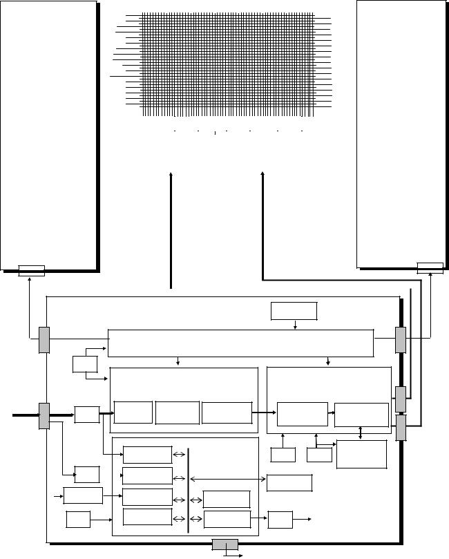
3.2Block Diagrams
3.2.1Signal Diagrams
|
|
|
|
|
|
|
|
|
|
|
|
|
|
|
|
|
|
|
|
|
|
|
|
|
|
|
|
|
|
X-SUS B. |
|
|
|
Y-SUS B. |
|
|
|
|
S |
|
|
|
|
|
|
|
|
|
|
|
|
|
|
|
|
|
|
X |
|
|
|
||||
|
|
|
|
|
|
|
|
|
|
|
|
|
|
|
|
|
|
|
|
|
|
|
|
|
|
|
|
|
X-SUS |
|
||
|
|
|
|
|
|
|
D |
|
|
|
|
|
|
|
|
|
|
|
|
|
|
|
|
|
|
B |
|
|
|
|
|
|
|
Y-SUS |
|
|
|
|
|
|
|
|
|
|
|
|
|
|
|
|
|
|
|
|
|
|
|
|
|
|
|
||||
|
|
|
|
|
M |
|
|
|
|
|
|
|
|
|
|
|
|
|
|
|
|
|
|
B |
|
|
|
|
EVEN SW |
|
||
|
EVEN SW |
|
|
|
|
|
|
|
|
|
|
|
|
|
|
|
|
|
|
|
|
|
|
|
|
|
|
|
||||
|
|
|
|
|
|
|
|
|
|
|
|
|
|
|
|
|
|
|
|
|
|
|
|
|
|
|
|
|
|
|
||
|
|
|
|
|
|
|
|
|
|
|
|
|
|
|
|
|
|
|
|
|
|
|
|
|
|
|
|
|
|
|
X-SCAN |
|
|
|
|
|
|
|
|
|
|
|
|
|
|
|
|
|
|
|
|
|
|
|
|
|
|
|
|
|
|
|
|
|
|
|
Y-SCAN |
|
|
|
|
|
|
|
|
|
|
|
|
|
|
|
|
|
|
|
|
|
|
|
|
|
|
|||||
|
|
|
|
|
|
|
|
|
|
|
|
|
|
|
|
|
|
|
|
|
|
|
|
|
|
|
|
|
EVEN SW |
|
||
|
EVEN SW |
|
|
|
|
S |
|
|
|
|
|
|
|
|
|
|
|
|
|
|
|
|
|
|
X |
|
|
|
|
|
||
|
|
|
|
|
|
|
|
|
|
|
|
|
|
|
|
|
|
|
|
|
|
|
|
|
|
|
|
|||||
|
|
|
|
|
|
|
|
|
|
|
|
|
|
|
|
|
|
|
|
|
|
|
|
|
|
|
|
|
||||
|
|
|
|
|
|
|
|
|
|
|
|
|
|
|
|
|
|
|
|
|
|
|
|
|
|
|
|
|
X-SUS |
|
||
|
|
|
|
|
|
|
|
|
|
|
|
|
|
|
|
|
|
|
|
|
||||||||||||
|
|
|
|
|
|
|
D |
|
|
|
|
|
|
|
|
|
|
|
|
|
|
|
|
|
|
B |
|
|
|
|
|
|
|
Y-SUS |
|
|
|
|
|
|
|
|
|
|
|
|
|
|
|
|
|
|
|
|
|
|
|
|
|
|
|
||||
|
|
|
|
|
|
|
|
|
|
|
|
|
|
|
|
|
|
|
|
|
|
|
|
|
|
|
ODD SW |
|
||||
|
ODD SW |
|
|
|
|
M |
|
|
|
|
|
|
|
|
|
|
|
|
|
|
|
|
|
|
B |
|
|
|
|
|
||
|
|
|
|
|
|
|
|
|
|
|
|
|
|
|
|
|
|
|
|
|
|
|
|
|
|
|
||||||
|
|
|
|
|
|
|
|
|
|
|
|
|
|
|
|
|
|
|
|
|
|
|
|
|
|
|
|
|
||||
|
|
|
|
|
|
|
|
|
|
|
|
|
|
|
|
|
|
|
|
|
|
|
|
|
|
|
|
|
|
|
X-SCAN |
|
|
|
|
|
|
|
|
|
|
|
|
|
|
|
|
|
|
|
|
|
|
|
|
|
|
|
|
|
|
|
|
|
|
|
Y-SCAN |
|
|
|
|
|
|
|
|
|
|
|
|
|
|
|
|
|
|
|
|
|
|
|
|
|
|
|
|
|
||
|
ODD SW |
|
|
|
|
|
|
ADM1 |
ADM2 |
|
ADM3 |
ADM4 |
ADM5 |
ADM6 |
ADM7 |
|
|
|
|
|
|
|
ODD SW |
|
||||||||
|
|
|
|
|
|
|
|
|
|
|
|
|
|
|||||||||||||||||||
|
|
|
|
|
|
|
|
|
|
|
|
|
|
|
|
|
|
|
|
|
|
|
|
|
|
|
|
|
|
|
|
|
|
POS /NEG |
|
|
|
|
|
|
|
|
ABUSL B |
|
|
ABUSR B. |
|
|
|
|
|
|
|
|
POS |
|
|||||||||
|
|
|
|
|
|
|
|
|
|
|
|
|
|
|
|
|
|
|
|
|
|
|
|
|
|
|
|
|
|
RESET SW |
|
|
RESET SW |
|
|
|
|
|
|
|
|
|
CN51 |
|
|
|
CN41 |
|
|
|
|
|
|
|
|
|
|||||||||
|
|
|
|
|
|
|
|
|
|
|
|
|
|
|
|
|
|
|
|
|
|
|||||||||||
|
|
|
|
|
|
|
|
|
|
|
|
|
|
|
|
|
|
|
|
|
|
|
|
|
|
|
|
|
|
|
|
|
|
|
|
|
|
|
|
|
|
|
|
|
|
|
|
|
|
|
|
|
|
|
|
|
|
|
|
|
|
|
|
|
|
|
|
|
|
|
|
|
|
|
|
|
|
|
|
|
|
|
|
|
|
|
|
|
|
|
|
|
|
|
|
|
|
|
CN31 |
CN21 |
|||
|
|
|
|
|
|
|
|
|
|
LOGIC B.
TIMMING ROM
CN3 |
CN2 |
SCAN CONTROLLER
|
OSC |
|
|
|
|
|
|
|
|
|
24MHz |
DATA PROCESSOR |
|
DATA CONVERTER |
|
||||
SIGNAL |
CN1 |
|
|
|
|
|
|
|
|
INPUT |
γ comp. |
RGB |
DITHER |
|
|
|
|
CN5 |
|
LVDS |
|
SUB FIELD |
MEMORY |
||||||
|
|
||||||||
|
|
GAIN |
/ERR DIF. |
|
PRC. |
CONTROLLER |
|
||
|
|
|
|
|
|
|
|
|
|
|
|
|
|
MPU |
|
|
|
CN4 |
|
|
|
V-SYNC cont. |
OSC |
OSC |
FRAME |
|
|||
|
|
|
|
MEMORY |
|
||||
|
|
|
|
|
|
|
|
|
|
|
I2C |
SCI. |
|
|
|
50MHz |
80MHz |
|
|
|
|
|
|
EEPROM |
|
|
|
||
|
|
|
|
|
|
|
|
|
|
|
Analog SW |
ailure DET. |
APC cont. |
|
|
Vrs |
|
|
|
|
|
|
|
|
|
|
|
|
|
|
OSC |
FLASH |
|
I/O |
|
D/A |
Vra |
|
|
|
|
|
Vrw |
|
|
||||
|
8MHz |
|
|
|
|
|
Vrx |
|
|
|
|
|
|
|
|
|
|
|
|
|
|
|
|
CN7 |
PFCgo |
|
|
|
|
|
|
|
|
|
Vsago |
|
|
|
|
|
|
|
|
|
Vcego |
|
|
|
|
|
|
|
|
-12- |
|
|
|
|
|

3.2.2 Power Diagrams |
|
|
|
|
Y-SUS B. |
|
|
X-SUS B. |
|
Y-SUS |
S |
X |
X-SUS |
|
D |
B |
EVEN SW |
||
EVEN SW |
||||
M |
B |
X-SCAN |
||
|
||||
Y-SCAN |
|
|
||
|
|
EVEN SW |
||
EVEN SW |
|
|
||
|
|
|
|
|
Y-SUS |
S |
|
|
|
|
X |
X-SUS |
|
|
|||
|
|
|
|
|
|
ODD SW |
|
|
||||||
|
|
ODD SW |
D |
|
|
|
|
B |
|
|
||||
|
|
Y-SCAN |
M |
|
|
|
|
B |
X-SCAN |
|
|
|||
|
|
|
|
|
|
|
|
|
|
|||||
|
|
|
|
|
|
|
|
ODD SW |
|
|
||||
|
|
ODD SW |
|
|
|
|
|
|
|
|
||||
|
|
POS/NEG |
ADM1 |
ADM2 ADM3 ADM4 ADM5 |
ADM6 |
ADM7 |
POS |
|
|
|||||
|
|
|
ABUSL B |
ABUSR B. |
|
|
||||||||
|
|
RESET SW |
|
RESET SW |
|
|
||||||||
|
|
|
|
|
Vcc 5V |
Va 55V |
Vcc 5V |
Va 55V |
|
|
|
|
|
|
|
|
|
|
|
|
|
|
|
|
Va |
Vb |
|
Vx |
|
|
|
|
|
|
CN32 |
|
CN52 |
|
CN42 |
CN22 |
-5V |
|
45V |
|
|
|
Vw |
|
160V |
|
|
|
|
|
|
||||
|
|
Vb |
|
-5V |
|
|
|
|
|
|
|
|
|
|
|
|
|
|
|
|
|
|
|
|
Vxwgo |
DC/DC |
|
||
|
|
|
|
|
|
|
|
|
|
|
CONVERTER |
|||
YFVCC1 |
YFVCC2 |
FVE5H |
|
|
|
Vra |
|
|
|
Vs 80V |
|
|||
5V |
5V |
|
|
17V |
|
|
|
|
|
|
|
|||
YFVE1 |
YFVE2 |
VE |
|
|
D/A |
Vrs |
|
|
|
|
|
|
||
|
|
Vrw |
|
|
XFVCC1 XFVCC2 |
VEW |
||||||||
17V |
|
17V |
|
17V |
CPUgo |
|
|
|
|
|||||
|
|
|
|
|
|
|
Vrx |
|
|
5V |
5V |
17V |
|
|
|
DC/DC |
|
|
PDPgo |
|
MPU |
|
|
|
XFVE1 |
XFVE2 |
VE |
||
|
|
|
|
|
|
|
|
17V |
17V |
|
17V |
|||
CONVERTER |
|
|
|
|
|
|
DC/DC |
|
||||||
|
|
|
|
|
|
|
Vcc 5V |
|
RST |
|
||||
|
|
|
|
|
|
|
|
Vrst |
|
|
||||
Vcc 5V |
|
Vs 80V |
|
|
|
Vpr2 3.3V |
|
|
CONVERTER |
|||||
|
|
|
|
|
|
|
|
|
|
|
|
|
|
|
|
|
|
|
|
|
|
|
LOGIC B. |
|
|
Vcc 5V |
|
|
|
CN33 |
|
|
|
|
|
|
CN6 |
|
|
|
Vs 80V |
|
||
|
|
|
|
|
|
|
|
|
|
|
||||
|
|
|
|
|
|
|
|
|
|
|
|
CN23 |
|
|
AC100 - |
|
|
10A |
|
|
|
|
|
|
|
|
|
|
|
240V |
|
|
|
|
380V |
|
55V |
|
|
|
|
|
||
|
|
|
|
PFC |
|
Va |
|
|
|
|
|
|||
|
|
|
|
|
|
|
|
CN65 |
|
|
|
|
||
|
|
|
|
|
|
|
|
|
|
|
|
|
||
|
|
CN61 |
|
|
|
Vsago |
5V |
|
|
|
|
|
||
|
|
|
|
|
|
|
|
|
|
|
|
|
||
|
|
|
|
|
|
|
|
|
|
|
|
|
|
|
|
|
|
|
|
|
|
|
Vcc |
|
CN68 |
|
|
|
|
|
|
|
|
|
Servce |
|
|
Vcego |
|
|
|
|
|
|
|
|
|
|
|
SW |
|
|
80V |
|
|
|
|
|
|
|
|
|
|
|
|
|
|
Vs |
CN67 |
|
|
|
|
|
|
|
|
|
|
PFCgo |
|
|
|
|
|
|
|
|
|
|
|
|
|
|
|
|
|
|
|
|
|
|
|
|
|
|
|
|
5/3.3V |
Vpr2 |
3.3V |
|
|
CN66 |
|
|
|
|
|
|
|
|
|
Vpr1 |
5V |
|
|
|
|
|
|
|
||
|
|
|
|
|
|
|
|
|
|
|
|
|||
|
|
|
|
Control |
Vsago |
|
|
|
|
CN64 |
|
|
|
|
PFCgo |
|
|
|
|
|
|
|
|
|
|
|
|||
|
|
|
PSU B. *1 |
Vra |
Vrs |
|
|
|
|
|
||||
Vsago |
|
|
|
*1:Power supply (jig) |
|
|
|
|||||||
|
|
|
|
|
|
|
|
|
|
|
||||
Vcego |
|
|
|
|
|
|
|
|
|
|
|
|
|
|
|
|
|
|
|
|
|
|
-13- |
|
|
|
|
|
|
3.3Function
3.3.1Logic board Function
(1) Data Processor
z γadjustment (1/2.2/2.4/2.6/2.8)
z NTSC/EBU format Color matrix Switch
z RGB gain Control White balance adjustment Amplitude limitation z Error Diffusion Technology (Grayscale adjustment)
z Dithering (Grayscale adjustment) z Burn-in Pattern generation
(2)Scan Controller
z Address driver control signal generator (ADM) z Scan driver control signal generator (SDM)
z X/Y sustain control signal generator
(3)Waveform ROM
z Waveform Pattern for drive / Timing memory
(4)MPU
z Synchronous detection z System control
z Driving voltage (Va,Vs,Vr,Vw) adjustment and tuning
z Abnormal watching (breakdown detection) / abnormal processing z Is (sustain) current control (sustain pulse control)
z Ia (address) current control (sub-field control) z External communication control
z Waveform ROM pattern writing
(5)EEPROM
z Control parameter memory
z The accumulation energizing time (Every hour). z Abnormal status memory (16 careers)
-14-

Sub |
Data |
|
Symbol |
|
Item |
|
|
Function |
Setting [hex] |
|
|
||||
Address |
bit |
|
|
|
|
RANGE |
INITIAL value |
|
|||||||
|
|
|
|
|
|
|
|
|
|
|
|||||
|
|
|
|
|
|
|
|
|
|
|
|
|
|||
|
|
|
|
|
|
|
|
|
|
|
|
|
|
|
|
00 |
7-0 |
|
MAPVER |
|
address MAP |
|
Indicates the version number of the address |
00 ~ FF |
01 UA1x/6x |
||||||
|
|
Version |
|
map. |
02 UA7x |
|
|||||||||
|
|
|
|
|
|
|
|
||||||||
|
|
|
|
|
|
|
|
|
|
|
|
|
|
|
|
|
7 |
|
ERRF |
|
update of Error |
|
Indicates that an error has occurred. |
|
|
|
|
||||
|
|
|
|
|
|
Flag |
|
It can be cleared with the ErrRST setting. |
0: Not updated |
|
|
|
|||
|
|
|
|
|
|
|
|
|
0 |
|
|
||||
|
|
|
|
|
|
|
|
|
If this flag is set, |
|
|
||||
|
|
|
|
|
|
|
|
|
1: Updated |
|
|
||||
|
|
|
|
|
|
|
|
|
• Error code is written. |
|
|
|
|||
|
|
|
|
|
|
|
|
|
|
|
|
|
|||
|
|
|
|
|
|
|
|
|
• |
Cannot enter the PDP-ON mode. |
|
|
|
|
|
01 |
6 |
|
OHRF |
|
update of |
|
Indicates that the drive hours are counted. |
0: Not updated |
0 |
|
|
||||
|
|
Operation Hours |
|
1: Updated |
|
|
|||||||||
|
|
|
|
|
|
Flag |
|
|
|
|
|
|
|
||
|
|
|
|
|
|
Power Shut |
|
Indicates that shutdown of the AC power is |
0: Not detected |
|
|
|
|||
|
5 |
|
PSDF |
|
|
detected and the PDP has executed the |
0 |
|
|
||||||
|
|
|
Down Flag |
|
OFF-sequence. It can be cleared with the |
1: Detected |
|
|
|||||||
|
|
|
|
|
|
|
|
|
|
||||||
|
|
|
|
|
|
|
|
|
PSDRST setting. |
|
|
|
|
||
|
4-0 |
|
CNDC |
|
Condition Code |
|
Indicates status of the module. |
- |
- |
|
|
||||
|
|
|
|
|
|
|
|
|
|
|
|
|
|
|
|
|
|
|
|
|
|
|
|
|
Indicates error code. |
|
|
|
|
||
02 |
7-0 |
|
ERRC |
|
Error Code |
|
The error codes of as many as 16 errors in |
00~FF |
00 |
|
|
||||
|
|
|
the past can be retrieved with the ERRS |
|
|
||||||||||
|
|
|
|
|
|
|
|
|
setting. . Same error code is not stored |
|
|
|
|
||
|
|
|
|
|
|
|
|
|
continuously. |
|
|
|
|
||
03 |
7-0 |
|
OHRH |
|
Operation Hours |
|
Indicates the higher 8 bits of the module |
00~FF |
00 |
|
|
||||
|
|
Higher bits |
|
driving hours. *1) |
|
|
|||||||||
|
|
|
|
|
|
|
|
|
|
|
|||||
04 |
7-0 |
|
OHRL |
|
Operation Hours |
|
Indicates the lower 8 bits of the module |
00~FF |
00 |
|
|
||||
|
|
Lower bits |
|
driving hours. *1) |
|
|
|||||||||
|
|
|
|
|
|
|
|
|
|
|
|||||
|
|
|
|
|
|
|
|
|
It selects the built-in test pattern signals of |
0: The single |
|
|
|
||
|
|
|
|
|
|
|
|
|
this display. This setting is valid when the |
color display |
|
|
|
||
|
|
|
|
|
|
|
|
|
PATON setting is 1. |
is switched |
|
|
|
||
|
|
|
|
|
|
|
|
|
|
|
|
every 2 |
|
|
|
|
|
|
|
|
|
|
|
|
|
|
|
seconds. A |
|
|
|
|
7 |
|
PATSEL |
|
Selecting |
|
|
|
|
total of 8 |
0 |
|
|
||
|
|
|
patterns |
|
|
|
|
colors are |
|
|
|||||
|
|
|
|
|
|
|
|
|
|
|
|
displayed. |
|
|
|
|
|
|
|
|
|
|
|
|
|
|
|
1: All white |
|
|
|
|
|
|
|
|
|
|
|
|
|
|
|
(Different |
|
|
|
|
|
|
|
|
|
|
|
|
|
|
|
from actual |
|
|
|
|
|
|
|
|
|
|
|
|
|
|
|
white.) |
|
|
|
|
|
|
|
|
|
|
|
|
Display of the built-in pattern signal in this |
0: Displaying |
|
|
|
||
|
|
|
|
|
|
Built-in pattern |
|
product is turned ON/OFF. |
the input |
|
|
|
|||
|
6 |
|
PATON |
|
|
|
|
|
signal |
0 |
|
|
|||
20 |
|
|
display is set to |
|
|
|
|
1: Displaying |
|
|
|||||
|
|
|
|
|
ON. |
|
|
|
|
|
|
|
|||
|
|
|
|
|
|
|
|
|
|
|
|
the built-in |
|
|
|
|
|
|
|
|
|
|
|
|
|
|
|
pattern |
|
|
|
|
|
|
|
|
|
Address |
|
The black screen is displayed. |
0: Blank |
|
|
|
|||
|
5 |
|
ADEN |
|
|
0 is set when the input video signal has |
1: Displaying |
1 |
|
|
|||||
|
|
|
data |
|
|
|
|||||||||
|
|
|
|
|
|
enable |
|
disturbance. |
the input |
|
|
|
|||
|
|
|
|
|
|
|
|
|
|
|
|
signal |
|
|
|
|
4 |
|
- |
|
|
- |
|
|
Be sure to use the display with the setting |
|
0~1 |
0 |
|
|
|
|
|
|
|
|
|
fixed to 0. |
|
|
|
||||||
|
|
|
|
|
|
|
|
|
|
|
|
|
|
||
|
3 |
|
- |
|
|
- |
|
|
Be sure to use the display with the setting |
0~1 |
1 UA1x/6x |
|
|||
|
|
|
|
|
|
fixed to 1. |
|||||||||
|
|
|
|
|
|
|
|
|
|
|
|
|
|||
|
|
|
|
|
|
|
|
|
Input reflection polarity setting |
0:Emits light by |
1 UA7x |
|
|||
|
3 |
|
DSPPRT |
|
DiSPlay |
|
|
|
|
LOW |
|
|
|
||
|
|
|
PaRiTy |
|
|
|
|
1:Emits light by |
|
|
|
||||
|
|
|
|
|
|
|
|
|
|
|
|
|
|||
|
|
|
|
|
|
|
|
|
|
|
|
High |
|
|
|
|
|
|
|
|
|
|
|
|
|
|
|
|
|
|
|
-15-
|
Sub |
Data |
|
|
Symbol |
|
Item |
|
Function |
|
|
Setting [hex] |
||||||||
|
|
|
|
|
|
|
|
|
|
|
|
|||||||||
Address |
|
bit |
|
|
|
|
|
|
RANGE |
INITIAL value |
||||||||||
|
|
|
|
|
|
|
|
|
|
|
|
|||||||||
|
|
|
|
|
|
|
|
|
|
|
|
|
|
|
|
|||||
|
|
|
|
|
|
|
|
|
|
|
|
|
|
|
|
|
|
|
|
|
20 |
|
|
|
|
|
|
|
|
|
Switches the interface power ON/OFF. |
|
|
|
|
|
|
||||
|
|
|
2 |
|
IFON |
|
Interface power |
Use this item when you want turn ON the |
0: Power OFF |
0 |
|
|||||||||
|
|
|
|
|
supply ON |
main power of the interface side only when |
1: Power ON |
|
||||||||||||
|
|
|
|
|
|
|
|
|
|
|
|
|||||||||
|
|
|
|
|
|
|
|
|
|
|
the PDPON is set to 0. This setting is |
|
|
|
|
|
|
|||
|
|
|
|
|
|
|
|
|
|
|
invalid when PDPON is set to 1. |
|
|
|
|
|
|
|||
|
|
|
|
|
|
|
|
|
High voltage |
Switches ON/OFF the high voltage power |
0: Power OFF |
|
|
|
||||||
|
|
|
1 |
PDPON |
|
power supply |
supply of PDP. |
0 |
|
|||||||||||
|
|
|
|
1: Power ON |
|
|||||||||||||||
|
|
|
|
|
|
|
|
|
ON |
|
|
|
|
|
|
|
||||
|
|
|
|
|
|
|
|
|
|
|
|
|
|
|
|
|
|
|
||
|
|
|
0 |
|
|
|
|
|
|
Be sure to use the display with the setting |
|
0~1 |
|
|
1 |
|
||||
|
|
|
|
|
|
|
|
|
fixed to 1. |
|
|
|
|
|||||||
|
|
|
|
|
|
|
|
|
|
|
|
|
|
|
|
|
||||
|
*1) It is not the one to guarantee brightness. |
|
|
|
|
|
|
|||||||||||||
|
Sub |
Data |
|
|
Symbol |
|
Item |
|
Function |
|
|
Setting[hex] |
||||||||
Address |
|
bit |
|
|
|
|
|
|
RANGE |
INITIAL value |
||||||||||
|
|
|
|
|
|
|
|
|
|
|
|
|||||||||
|
|
|
|
|
|
|
|
|
|
|
|
|
|
|
|
|||||
|
|
|
|
|
|
|
|
|
|
|
|
|
|
|
|
|
|
|
|
|
|
|
|
7-5 |
|
- |
|
|
- |
|
|
Be sure to use the display with the setting |
|
|
0~7 |
|
0 UA1x/6x |
||||
|
|
|
|
|
|
|
|
fixed to 0. |
|
|
|
|||||||||
|
|
|
|
|
|
|
|
|
|
|
|
|
|
|
|
|
|
|
||
|
|
|
7-6 |
|
- |
|
|
- |
|
|
Be sure to use the display with the setting |
|
|
0~7 |
|
0 UA7x |
||||
|
|
|
|
|
|
|
|
fixed to 0. |
|
|
|
|||||||||
|
|
|
|
|
|
|
|
|
|
|
|
|
|
|
|
|
|
|
||
|
|
|
|
|
|
|
|
|
|
|
|
Selecting the color correction modes. |
|
0: |
Luminance |
|
|
|
||
|
|
|
4 |
|
CCFMD |
|
Color correction |
|
Valid when the CCFON setting is 1 |
|
|
has priority. |
0 |
|
||||||
|
|
|
|
|
mode |
|
|
|
|
1: Gradation |
|
|||||||||
|
|
|
|
|
|
|
|
|
|
|
|
|
|
|
|
|||||
|
|
|
|
|
|
|
|
|
|
|
|
|
|
|
|
has priority |
|
|
|
|
|
|
|
3 |
|
DCBON |
|
Dynamic Color |
|
Tracking correction of white balance |
|
0: OFF |
|
|
|
||||||
|
|
|
|
|
|
between the high luminance and the low |
|
0 |
|
|||||||||||
|
|
|
|
|
Balance |
|
|
1: ON |
|
|||||||||||
|
|
|
|
|
|
|
|
|
|
luminance. |
|
|
|
|
||||||
|
|
|
|
|
|
|
|
|
|
|
|
|
|
|
|
|
|
|
||
|
|
|
|
|
|
|
|
|
|
|
|
|
|
|
|
|
|
|
|
|
|
|
|
|
|
|
|
|
|
|
|
|
When a picture with high luminance/small |
|
|
|
|
|
|
|
|
|
|
|
|
|
|
|
|
|
|
|
|
area is displayed for about 3 minutes or |
|
|
|
|
|
|
|
|
|
|
|
2 |
|
HAON |
|
Heat APC |
|
longer, the number of pulses is reduced to |
|
0: OFF |
|
|
|
||||||
|
|
|
|
|
|
about 20% at a maximum. This item can be |
|
0 |
|
|||||||||||
|
|
|
|
|
function |
|
|
1: |
ON |
|
||||||||||
21 |
|
|
|
|
|
|
|
|
used to reduce panel temperature/extend |
|
|
|
|
|||||||
|
|
|
|
|
|
|
|
|
|
useful life when the display is used to |
|
|
|
|
|
|
|
|||
|
|
|
|
|
|
|
|
|
|
|
|
|
|
|
|
|
|
|
||
|
|
|
|
|
|
|
|
|
|
|
|
show a still image. |
|
|
|
|
|
|
|
|
|
|
|
1 |
|
- |
|
|
- |
|
|
Be sure to use the display with the setting |
|
|
0~1 |
|
0 |
|
|||
|
|
|
|
|
|
|
|
fixed to 0. |
|
|
|
|
||||||||
|
|
|
|
|
|
|
|
|
|
|
|
|
|
|
|
|
|
|
||
|
|
|
|
|
|
|
|
|
|
|
|
Whether the register value is reflected to |
|
|
|
|
|
|
|
|
|
|
|
|
|
|
|
|
|
|
|
|
the operating status of this product, |
|
|
|
|
|
|
|
|
|
|
|
|
|
|
|
|
|
|
|
|
selected by this item. |
|
|
|
|
|
|
|
|
|
|
|
|
|
|
|
|
|
|
|
|
The following switch is executed. |
|
|
|
|
|
|
|
|
|
|
|
0 |
|
DSETEN |
|
Data |
|
0: The received register value is reflected |
|
0: |
Invalid |
1 |
|
||||||
|
|
|
|
|
set |
|
from the next field. |
|
1: |
Valid |
|
|||||||||
|
|
|
|
|
|
|
|
|
enable |
|
1: The received register value is stored so |
|
|
|
|
|||||
|
|
|
|
|
|
|
|
|
|
|
|
|
|
|
|
|
||||
|
|
|
|
|
|
|
|
|
|
|
|
that the DSET setting is reflected from |
|
|
|
|
|
|
|
|
|
|
|
|
|
|
|
|
|
|
|
|
the next field. |
|
|
|
|
|
|
|
|
|
|
|
|
|
|
|
|
|
|
|
|
(DSET setting: Setting bit 0 of address |
|
|
|
|
|
|
|
|
|
|
|
|
|
|
|
|
|
|
|
|
FF) |
|
|
|
|
|
|
|
|
22 |
|
7 |
|
CCFON |
|
Color correction |
|
Color collection process is turned |
|
0: |
OFF |
0 |
|
|||||||
|
|
|
|
|
|
ON/OFF. |
|
1: ON |
|
|||||||||||
|
|
|
|
|
|
|
|
|
|
|
|
|
|
|
|
|||||
|
|
|
|
|
|
|
|
|
|
|
|
|
|
|
|
|
|
|
|
|
|
|
|
|
|
|
|
|
|
Color correction |
|
Color collection process is switched. |
|
0: NTSC |
|
|
|
||||
|
|
|
6 |
|
CCFORM |
|
|
This item is valid when CCFON setting is |
|
0 |
|
|||||||||
|
|
|
|
|
format |
|
|
1: EBU |
|
|||||||||||
|
|
|
|
|
|
|
|
|
1. |
|
|
|
|
|
||||||
|
|
|
|
|
|
|
|
|
|
|
|
|
|
|
|
|
|
|
||
|
|
|
5-3 |
|
- |
|
|
- |
|
|
Be sure to use the display with the setting |
|
|
0~7 |
|
0 |
|
|||
|
|
|
|
|
|
|
|
fixed to 0. |
|
|
|
|
||||||||
|
|
|
|
|
|
|
|
|
|
|
|
|
|
|
|
|
|
|
||
|
Sub |
|
|
Data |
|
|
Symbol |
|
Item |
|
|
Function |
|
|
|
Setting [hex] |
|
|||
|
|
|
|
|
|
|
|
|
|
|
|
|
|
|
|
|
|
|
|
|
-16-
|
Addre |
|
bit |
|
|
|
|
|
|
|
|
|
|
RANGE |
|
|
INITIAL |
|
|
|
ss |
|
|
|
|
|
|
|
|
|
|
|
|
|
|
value |
|
||
|
|
|
|
|
|
|
|
|
|
|
|
|
|
|
|
|
|
||
|
|
|
|
|
|
|
|
|
|
|
|
Reverse γ correction level is set. |
0: |
OFF |
|
|
|
||
|
|
|
|
|
|
|
|
|
|
|
|
The setup 7 is the test mode. Do not select |
1: |
1.0 th power |
|
|
|
||
|
|
|
|
|
|
|
|
|
|
|
|
2: |
2.2 nd |
|
|
|
|||
|
|
|
|
|
|
|
|
|
|
|
|
the setup 7. |
|
|
|
||||
|
|
|
|
|
|
|
|
|
Selecting the |
|
When the setup 6 is selected, setting of the |
|
|
power |
|
|
|
||
|
|
|
|
|
|
|
|
|
|
3: |
2.4 th power |
|
|
|
|||||
22 |
|
2-0 |
|
GAMSEL |
|
reverse γ |
|
addressed in the range of 31~51 become |
2 |
|
|||||||||
|
|
|
|
|
|
|
|
|
correction |
|
valid. |
4: |
2.6 th power |
|
|
|
|||
|
|
|
|
|
|
|
|
|
|
|
|
|
5: |
2.8 th power |
|
|
|
||
|
|
|
|
|
|
|
|
|
|
|
|
|
|
6: USER |
|
|
|
||
|
|
|
|
|
|
|
|
|
|
|
|
|
|
7: TEST |
|
|
|
||
|
|
|
|
|
|
CONTRAS |
|
|
|
|
Peak luminance is adjusted. |
|
|
|
|
|
|
|
|
23 |
|
7-0 |
|
|
|
Peak luminance |
|
When the display picture load is heavy, the |
|
|
00~FF |
|
FF |
||||||
|
|
|
T |
|
|
|
|
|
|||||||||||
|
|
|
|
|
|
|
|
|
|
peak luminance is automatically limited. |
|
|
|
|
|
|
|
||
|
|
|
|
|
|
|
|
|
|
|
|
|
|
|
|
|
|
|
|
|
|
|
|
|
|
|
|
|
|
|
|
|
|
|
|
|
|
|
|
24 |
|
7-0 |
|
R-RATIO |
|
R ratio |
|
White balance is adjusted. |
|
|
00~FF |
|
FF |
||||||
|
|
|
|
Use the display with at least one item being |
|
|
|
||||||||||||
|
|
|
|
|
|
|
|
|
|
|
|
|
|
|
|
|
|
|
|
25 |
|
7-0 |
|
G-RATIO |
|
G ratio |
|
set to FF (hex). |
|
|
00~FF |
|
FF |
||||||
|
|
|
|
|
|
|
|
||||||||||||
|
|
|
|
|
|
|
|
|
|
|
|
|
|
|
|
|
|||
26 |
|
7-0 |
|
B-RATIO |
B ratio |
|
|
|
|
00~FF |
|
FF |
|||||||
|
|
|
|
|
|
|
|
|
|
|
|
|
|
|
|
|
|
|
|
|
|
|
|
|
|
|
|
|
|
|
|
This item implements control to return the |
|
0: Normal |
|
|
|
||
|
|
|
|
|
|
|
|
|
Clearing the IRQ |
|
IRQ signal from "HIGH" to "Low" level |
|
|
|
|
||||
|
|
|
7 |
|
IRQRST |
|
|
when an error occurs. When this item is set |
|
1: IRQ signal |
0 |
|
|||||||
|
|
|
|
|
output signal |
|
|
|
|||||||||||
|
|
|
|
|
|
|
|
|
|
|
|
to 1, the IRQ signal is returned to "Low" |
|
|
clear |
|
|
|
|
|
|
|
|
|
|
|
|
|
|
|
|
level. |
|
|
|
|
|
|
|
|
|
|
|
|
|
|
|
|
|
|
|
This item implements control to return the |
|
0: Normal |
|
|
|
||
|
|
|
6 |
|
ERRRST |
|
Clearing the |
|
ERRF flag to 0 when an error occurs. |
|
0 |
|
|||||||
|
|
|
|
|
|
When this item is set to 1, this setting |
|
1: ERRF |
|
||||||||||
|
|
|
|
|
ERRF flag |
|
|
|
|||||||||||
|
|
|
|
|
|
|
|
|
|
|
|
automatically returns to 0 after returning |
|
|
flag clear |
|
|
|
|
|
|
|
|
|
|
|
|
|
|
|
|
the ERRF flag to 0. |
|
|
|
|
|
|
|
|
|
|
5 |
|
|
- |
|
|
- |
|
|
Be sure to use the display with the setting |
|
|
|
|
|
|
|
|
|
|
|
|
|
|
|
|
|
|
|
fixed to 0. |
0~1 |
|
|
0 UA1x/6x |
|||
|
|
|
|
|
|
|
|
|
|
|
|
|
|
|
|
|
|
|
|
|
|
|
5 |
|
|
OHRRST |
|
Clearing the |
|
The control by which the OHRF flag is |
|
0: Normal |
|
|
|
||||
|
|
|
|
|
|
|
|
|
OHRF flag |
|
returned to 0 is done. This setting |
|
|
0 UA7x |
|||||
|
27 |
|
|
|
|
|
|
|
|
|
|
automatically returns to the state of 0 after |
|
1: OHRF |
|
||||
|
|
|
|
|
|
|
|
|
|
|
|
returning 0 the ERRF flag when this |
|
|
flag clear |
|
|
|
|
|
|
|
|
|
|
|
|
|
|
|
|
setting is set to one. |
|
|
|
|
|
|
|
|
|
|
4 |
|
|
PSDRST |
|
Clearing the |
|
This item exercise control to return the |
|
0: Normal |
|
|
|
||||
|
|
|
|
|
|
|
|
|
PSDF flag |
|
PSDF flag to 0 when this machine |
|
|
|
|
||||
|
|
|
|
|
|
|
|
|
|
|
|
performs the OFF sequence at AC power |
|
1: PSDF |
0 |
|
|||
|
|
|
|
|
|
|
|
|
|
|
|
shutdown. When this item is set to 1, this |
|
|
flag |
|
|
|
|
|
|
|
|
|
|
|
|
|
|
|
|
setting automatically returns to 0 after |
|
|
clear |
|
|
|
|
|
|
|
|
|
|
|
|
|
|
|
|
returning the PSDF flag to 0. |
|
|
|
|
|
|
|
|
|
|
3-0 |
|
ERRS |
|
Error code |
|
When this setting is changed and the |
|
0: Latest error |
|
|
|
|||||
|
|
|
|
|
|
|
|
|
selection |
|
ERRC setting is read out, the error |
|
1: Previous |
|
|
|
|||
|
|
|
|
|
|
|
|
|
|
|
|
contents (as many as 16 errors) of the |
|
|
|
|
|||
|
|
|
|
|
|
|
|
|
|
|
|
|
|
error |
|
|
|
||
|
|
|
|
|
|
|
|
|
|
|
|
module that have occurred in the past can |
|
|
|
|
|
||
|
|
|
|
|
|
|
|
|
|
|
|
2: |
|
|
|
|
|
||
|
|
|
|
|
|
|
|
|
|
|
|
be checked. |
|
|
0 |
|
|||
|
|
|
|
|
|
|
|
|
|
|
|
If more than 16 errors have occurred, the |
| |
|
|
|
|
|
|
|
|
|
|
|
|
|
|
|
|
|
|
error code is updated starting from the |
|
E: |
|
|
|
|
|
|
|
|
|
|
|
|
|
|
|
|
|
oldest error. |
|
|
|
|
|
|
|
|
|
|
|
|
|
|
|
|
|
|
|
|
F:Oldest error |
|
|
|
|||
|
|
|
|
|
|
|
|
|
|
|
|
|
|
|
|
|
|||
28 |
|
7-6 |
|
|
- |
|
|
- |
|
|
Be sure to use the display with the setting |
0~3 |
|
|
0 UA1x/6x |
||||
|
|
|
|
|
|
|
|
|
fixed to 0. |
|
|
||||||||
|
|
|
|
|
|
|
|
|
|
|
|
|
|
|
|
|
|
|
|
|
|
|
7 |
|
|
PWMP |
|
Power Maximam |
|
The PWMAX setting is switched to |
|
When password |
|
0 UA7x |
|||||
|
|
|
|
|
|
|
constant brightness (peak electric power) |
|
|
is set |
|
||||||||
|
|
|
|
|
|
|
|
|
peek control |
|
control. The password setting is necessary |
|
0:OFF 1:ON |
|
|
|
|||
|
|
|
|
|
|
|
|
|
|
|
|
to turn on this setting. |
|
|
|
|
|||
|
Sub |
|
Data |
|
|
Symbol |
|
|
Item |
|
|
Function |
|
|
Setting [hex] |
|
|||
|
|
|
|
|
|
|
|
|
|
|
|
|
|
|
|
|
|
|
|
-17-
Addre |
bit |
RANGE |
INITIAL |
ss |
|
value |
|
|
|
|
|
|
6 |
|
- |
|
- |
|
|
|
Be sure to use the display with the setting |
0-3 |
|
0 UA7x |
||||||||
|
|
|
|
|
|
|
|
fixed to 0. |
|
|
||||||||||||
|
|
|
|
|
|
|
|
|
|
|
|
|
|
|
|
|
|
|
|
|||
|
|
|
|
|
|
|
|
|
|
|
|
|
|
Sets the maximum power consumption. |
|
|
|
|
|
|||
|
|
|
|
|
|
|
|
|
|
|
|
|
|
Set this item in accordance with the status |
|
|
|
|
|
|||
|
|
|
|
|
|
|
|
|
|
|
|
|
|
of the machine. |
|
|
0: −20W |
|
|
|||
28 |
|
|
|
|
|
|
|
|
|
|
|
|
Make sure that the respective parts' |
|
1: −10W |
|
|
|||||
|
5-4 |
|
PWMAX |
|
|
Maximum power |
|
|
temperature/panel temperature stays within |
|
2: ±0W |
2 UA1x/6x |
||||||||||
|
|
|
|
|
|
consumption |
|
|
the specifications. If the setting is set to 3, |
|
||||||||||||
|
|
|
|
|
|
|
|
|
|
|
|
|
3: +10W |
|
|
|||||||
|
|
|
|
|
|
|
|
|
|
|
|
|
|
power consumption increases to a level |
|
|
|
|||||
|
|
|
|
|
|
|
|
|
|
|
|
|
|
exceeding the standard consumption. Be |
|
|
|
|
|
|||
|
|
|
|
|
|
|
|
|
|
|
|
|
|
sure to execute the heat dissipation design |
|
|
|
|
|
|||
|
|
|
|
|
|
|
|
|
|
|
|
|
|
so that respective parts' temperature/panel |
|
|
|
|
|
|||
|
|
|
|
|
|
|
|
|
|
|
|
|
|
temperature stays within the specifications. |
|
|
|
|
|
|||
|
|
|
|
|
|
|
|
|
|
|
|
|
|
PWMP |
|
Setting of the maximum electric |
|
0: 0W |
|
|
||
|
|
|
|
|
|
|
|
|
|
|
|
=0 |
|
power. |
|
|
1: +10W |
|
|
|||
|
|
|
|
|
|
|
|
|
|
|
|
|
|
|
|
|
|
|
|
|
||
|
|
|
|
|
|
|
|
|
|
|
|
|
|
|
|
|
|
|
2: +20W |
|
|
|
|
|
|
5-4 |
|
PWMAX |
|
|
Maximum power |
|
|
|
|
|
|
|
3: +30W |
2 UA7x |
|||||
|
|
|
|
|
|
|
|
|
|
|
|
|
|
|
||||||||
|
|
|
|
|
|
consumption |
|
|
PWMP |
|
Setting of peak electric power. |
|
0: −20W |
|||||||||
|
|
|
|
|
|
|
|
|
|
|
|
|
|
|
|
|||||||
|
|
|
|
|
|
|
|
|
|
|
|
=1 |
|
Electric power by which electric |
|
1: −10W |
|
|
||||
|
|
|
|
|
|
|
|
|
|
|
|
|
|
|
|
power is permitted in addition to |
|
|
|
|||
|
|
|
|
|
|
|
|
|
|
|
|
|
|
|
|
improve practical brightness to |
|
2: ±0W |
|
|
||
|
|
|
|
|
|
|
|
|
|
|
|
|
|
|
|
the maximum electric power set |
|
3: +10W |
|
|
||
|
|
|
|
|
|
|
|
|
|
|
|
|
|
|
|
3:+10W |
|
|
|
|
||
|
|
|
|
|
|
|
|
|
|
|
|
|
|
|
|
|
|
|
|
|
|
|
|
|
|
3-0 |
|
|
- |
|
|
|
- |
|
|
|
Be sure to use the display with the setting |
|
0-F |
0 |
|
||||
|
|
|
|
|
|
|
|
|
|
|
fixed to 0. |
|
|
|
||||||||
|
|
|
|
|
|
|
|
|
|
|
|
|
|
|
|
|
|
|
|
|
|
|
29 |
|
|
|
|
|
|
|
|
|
|
|
|
Password of peak electric power |
|
51: Permission |
|
|
|||||
|
|
|
|
PWM |
|
|
Password of peak |
|
|
setting.The password is described to the |
|
of PWMP |
|
|
||||||||
|
|
|
7-0 |
|
|
|
|
|
|
delivery specifications. When the password |
|
ON |
FF UA7x |
|||||||||
|
|
|
|
|
PASS |
|
|
electric power |
|
|
setting is normally done, the reading value |
|
Another: |
|||||||||
|
|
|
|
|
|
|
|
setting |
|
|
|
|
|
|||||||||
|
|
|
|
|
|
|
|
|
|
|
|
|
|
of the real thing ground becomes 51. |
|
Prohibition |
|
|
||||
|
|
|
|
|
|
|
|
|
|
|
|
|
|
|
|
|
|
|
|
|
||
|
|
|
|
|
|
|
|
|
|
|
|
|
|
|
|
|
|
|
|
|
||
|
|
|
|
|
|
|
|
|
|
|
|
|
|
The maximum |
When the amount of |
|
|
|
|
|
||
|
|
|
|
|
|
|
|
|
|
|
|
|
|
electric power |
an over electric |
|
|
|
|
|
||
|
2C |
7-0 |
|
|
PsTPW |
|
|
Ps-Tank PoWer |
|
|
setting: |
|
|
power becomes |
|
00-FF |
1E UA7x |
|||||
|
|
|
|
|
|
|
The maximum |
PsTPW×PsTTM or |
|
|||||||||||||
|
|
|
|
|
|
|
|
|
|
|
|
|
|
less at PWMP=1, the |
|
|
|
|
|
|||
|
|
|
|
|
|
|
|
|
|
|
|
|
|
over electric power |
|
|
|
|
|
|||
|
|
|
|
|
|
|
|
|
|
|
|
|
|
control by which |
|
|
|
|
|
|||
|
|
|
|
|
|
|
|
|
|
|
|
|
|
from +10W |
|
|
|
|
|
|||
|
|
|
|
|
|
|
|
|
|
|
|
|
|
brightness is lowered |
|
|
|
|
|
|||
|
|
|
|
|
|
|
|
|
|
|
|
|
|
Time which can |
is done. |
|
|
|
|
|
||
|
2D |
7-0 |
|
|
PsTTM |
|
|
Ps-Tank TiMe |
|
|
operate by the |
|
|
00-FF |
3C UA7x |
|||||||
|
|
|
|
|
|
|
maximum over |
|
|
|||||||||||||
|
|
|
|
|
|
|
|
|
|
|
|
|
|
electric power |
|
|
|
|
|
|
||
|
|
|
|
|
|
|
|
|
|
|
|
|
|
(*10sec) |
|
|
|
|
|
|
||
31 |
|
7-0 |
|
|
GAM00 |
|
|
Reverse γ |
|
|
Sets the input level that implements the |
|
00~FF |
|
1F |
|||||||
|
|
|
|
|
correction DC |
|
|
forced 0 [LSB] output. |
|
|
||||||||||||
|
|
|
|
|
|
|
|
|
|
|
|
|
|
|
|
|
||||||
32 |
|
7-2 |
|
- |
|
|
|
<no use> |
- |
|
|
|
|
00~FF |
|
00 |
|
|||||
|
1-0 |
|
|
GAM01 |
|
|
|
|
|
|
|
|
|
|
|
|
|
|||||
|
|
|
|
[9: 8] |
|
|
|
Reverse γ |
|
|
Reverse γ coefficient value is set. |
|
|
|
|
|
||||||
|
|
|
|
|
|
|
|
|
|
|
|
|
|
|
||||||||
33 |
|
7-0 |
|
|
GAM01 |
|
|
coefficient 01 |
|
|
Input |
Output value of 8 [LSB] |
|
00~FF |
|
04 |
|
|||||
|
|
[7: 0] |
|
|
|
|
|
|
|
|
|
|
|
|
|
|
||||||
|
|
|
|
|
|
|
|
|
|
|
|
|
|
|
|
|
|
|
|
|
||
|
|
|
7-3 |
|
- |
|
|
|
<no use> |
- |
|
|
|
|
00~FF |
|
00 |
|
||||
34 |
|
2-0 |
|
|
GAM02 |
|
|
|
|
|
|
|
|
|
|
|
|
|
||||
|
|
|
|
|
|
|
|
|
|
|
|
|
|
|
|
|
|
|||||
|
|
|
|
[10: 8] |
|
|
|
Reverse γ |
|
|
Reverse γ coefficient value is set. |
|
|
|
|
|
||||||
|
|
|
|
|
|
|
|
|
|
|
|
|
|
|
||||||||
|
|
|
|
|
|
|
|
|
|
correction 02 |
|
|
Input Output value of 16 [LSB] |
|
00~FF |
|
24 |
|
||||
35 |
|
7-0 |
|
|
GAM02 |
|
|
|
|
|
||||||||||||
|
|
|
|
|
|
|
|
|
|
|
|
|
|
|
|
|
|
|||||
|
|
[7: 0] |
|
|
|
|
|
|
|
|
|
|
|
|
|
|
|
|
||||
|
|
|
|
|
|
|
|
|
|
|
|
|
|
|
|
|
|
|
|
|
||
|
|
|
|
|
|
|
|
|
|
|
|
|
|
|
|
|
|
|||||
|
|
|
|
|
|
|
|
|
|
|
|
|
|
|
|
|
||||||
|
Sub |
|
Data |
|
|
Symbol |
|
|
|
Item |
|
|
|
Function |
|
|
Setting [hex] |
|
||||
|
|
|
|
|
|
|
|
|
|
|
|
|
|
|
|
|
|
|
|
|
|
|
-18-

Addre |
bit |
RANGE |
INITIAL |
ss |
|
value |
|
|
|
|
|
|
7-4 |
|
- |
|
|
<no use> |
- |
|
|
|
|
|
|
|
36 |
|
3-0 |
|
GAM03 |
|
Reverse γ |
|
Reverse γ coefficient value is set. |
|
00-FF |
|
00 |
|
|||
|
|
|
|
[11:8] |
|
|
correction 03 |
|
Input Output value of 24 [LSB] |
|
|
|
|
|
||
|
|
|
|
|
|
|
|
|
|
|
|
|
||||
|
|
|
|
|
|
|
|
|
|
|
|
|
|
|
|
|
37 |
|
7-0 |
|
GAM03 |
|
|
|
|
|
|
00~FF |
|
58 |
|
||
|
|
[7: 0] |
|
|
|
|
|
|
|
|
|
|||||
|
|
|
|
|
|
|
|
|
|
|
|
|
|
|
|
|
|
|
|
|
|
|
|
|
|
|
|
|
|
|
|
|
|
|
|
|
7-4 |
|
- |
|
|
<no use> |
- |
|
|
|
|
|
|
|
38 |
|
3-0 |
|
GAM04 |
|
Reverse γ |
|
Reverse γ coefficient value is set. |
|
00~FF |
|
00 |
|
|||
|
|
|
|
[11: 8] |
|
|
correction 04 |
|
Input Output value of 32 [LSB] |
|
|
|
|
|
||
|
|
|
|
|
|
|
|
|
|
|
|
|
||||
|
|
|
|
|
|
|
|
|
|
|
|
|
|
|
|
|
39 |
|
7-0 |
|
GAM04 |
|
|
|
|
|
|
00~FF |
|
A7 |
|||
|
|
[7: 0] |
|
|
|
|
|
|
|
|
||||||
|
|
|
|
|
|
|
|
|
|
|
|
|
|
|
|
|
|
|
|
7-5 |
|
- |
|
|
<no use> |
- |
|
|
|
|
|
|
|
|
3A |
4-0 |
|
GAM05 |
|
|
|
|
|
|
00~FF |
|
01 |
|
||
|
|
|
|
[12: 8] |
|
|
Reverse γ |
|
Reverse γ coefficient value is set. |
|
|
|
|
|
||
|
|
|
|
|
|
|
|
|
|
|
|
|
||||
|
|
|
7-1 |
|
GAM05 |
|
correction 05 |
|
Input |
Output value of 40 [LSB] |
|
|
|
|
|
|
|
3B |
|
[7: 1] |
|
|
|
|
|
|
|
00~FF |
|
12 |
|
||
|
|
|
|
|
|
|
|
|
|
|
|
|||||
|
|
|
0 |
|
- |
|
|
<no use> |
- |
|
|
|
|
|
|
|
|
|
|
7-5 |
|
- |
|
|
<no use> |
- |
|
|
|
|
|
|
|
|
3C |
4-0 |
|
GAM06 |
|
|
|
|
|
|
00~FF |
|
01 |
|
||
|
|
|
|
[12: 8] |
|
|
Reverse γ |
|
Reverse γ coefficient value is set. |
|
|
|
|
|
||
|
|
|
|
|
|
|
|
|
|
|
|
|
||||
|
|
|
7-1 |
|
GAM06 |
|
correction 06 |
|
Input |
Output value of 48 [LSB] |
|
|
|
|
|
|
|
3D |
|
[7: 1] |
|
|
|
|
|
|
|
00~FF |
|
9A |
|||
|
|
|
|
|
|
|
|
|
|
|
||||||
|
|
|
|
|
|
|
|
|
|
|
|
|
|
|
|
|
|
|
|
0 |
|
- |
|
|
<no use> |
- |
|
|
|
|
|
|
|
|
|
|
7-5 |
|
- |
|
|
<no use> |
- |
|
|
|
|
|
|
|
|
3E |
4-0 |
|
GAM07 |
|
|
|
|
|
|
00~FF |
|
02 |
|
||
|
|
|
|
[12: 8] |
|
|
Reverse γ |
|
Reverse γ coefficient value is set. |
|
|
|
|
|
||
|
|
|
|
|
|
|
|
|
|
|
|
|
||||
|
|
|
7-2 |
|
GAM07 |
|
correction 07 |
|
Input |
Output value of 56 [LSB] |
|
|
|
|
|
|
|
3F |
|
[7: 2] |
|
|
|
|
|
|
|
00~FF |
|
40 |
|
||
|
|
|
|
|
|
|
|
|
|
|
|
|||||
|
|
|
|
|
|
|
|
|
|
|
|
|
|
|
|
|
|
|
|
1-0 |
|
- |
|
|
<no use> |
- |
|
|
|
|
|
|
|
|
|
|
7-5 |
|
- |
|
|
<no use> |
- |
|
|
|
|
|
|
|
40 |
|
4-0 |
|
GAM08 |
|
|
|
|
|
|
00~FF |
|
03 |
|
||
|
|
|
|
[12: 8] |
|
|
Reverse γ |
|
Reverse γ coefficient value is set. |
|
|
|
|
|
||
|
|
|
|
|
|
|
|
|
|
|
|
|
||||
|
|
|
7-2 |
|
GAM08 |
|
correction 08 |
|
Input |
Output value of 64 [LSB] |
|
|
|
|
|
|
41 |
|
|
[7: 2] |
|
|
|
|
|
|
|
00~FF |
|
04 |
|
||
|
|
|
|
|
|
|
|
|
|
|
|
|||||
|
|
|
|
|
|
|
|
|
|
|
|
|
|
|
|
|
|
|
|
1-0 |
|
- |
|
|
<no use> |
- |
|
|
|
|
|
|
|
|
|
|
7-6 |
|
- |
|
|
<no use> |
- |
|
|
|
|
|
|
|
42 |
|
5-0 |
|
GAM09 |
|
|
|
|
|
|
00~FF |
|
04 |
|
||
|
|
|
|
[13: 8] |
|
|
Reverse γ |
|
Reverse γ coefficient value is set. |
|
|
|
|
|
||
|
|
|
|
|
|
|
|
|
|
|
|
|
||||
|
|
|
7-4 |
|
GAM09 |
|
correction 09 |
|
Input |
Output value of 80 [LSB] |
|
|
|
|
|
|
43 |
|
|
[7: 4] |
|
|
|
|
|
|
|
00~FF |
|
F0 |
|||
|
|
|
|
|
|
|
|
|
|
|
||||||
|
|
|
|
|
|
|
|
|
|
|
|
|
|
|
|
|
|
|
|
3-0 |
|
- |
|
|
<no use> |
- |
|
|
|
|
|
|
|
|
|
|
|
|
|
|
|
|
|
|
|
|
|
|
|
|
|
Sub |
|
Data |
|
Symbol |
|
|
Item |
|
Function |
|
|
Setting [hex] |
|
|
|
|
|
|
|
|
|
|
|
|
|
|
|
|
|
|
|
|
-19-

Addre |
bit |
RANGE |
INITIAL |
ss |
|
value |
|
|
|
|
|
|
7-6 |
|
- |
|
|
<no use> |
- |
|
|
|
|
|
|
||
44 |
|
5-0 |
|
|
GAM10 |
|
Reverse γ |
|
Reverse γ coefficient value is set. |
|
00~FF |
|
07 |
|
|||
|
|
|
|
[13: 8] |
|
|
correction 10 |
|
Input |
Output value of 96 [LSB] |
|
|
|
|
|
||
|
|
|
|
|
|
|
|
|
|
|
|
|
|||||
|
|
|
|
|
|
|
|
|
|
|
|
|
|
|
|
|
|
|
|
|
7-4 |
|
|
GAM10 |
|
Reverse γ |
|
Reverse γ coefficient value is set. |
|
|
|
|
|
||
45 |
|
|
[7: 4] |
|
|
correction 10 |
|
Input |
Output value of 96 [LSB] |
|
00~FF |
|
60 |
|
|||
|
|
|
|
|
|
|
|
|
|||||||||
|
|
|
|
|
|
|
|
|
|
|
|
|
|
|
|
|
|
|
|
|
3-0 |
|
- |
|
|
<no use> |
- |
|
|
|
|
|
|
||
|
|
|
7-6 |
|
- |
|
|
<no use> |
- |
|
|
|
|
|
|
||
46 |
|
5-0 |
|
|
GAM11 |
|
|
|
|
|
|
00~FF |
|
0A |
|||
|
|
|
|
[13: 8] |
|
|
Reverse γ |
|
Reverse γ coefficient value is set. |
|
|
|
|
|
|||
|
|
|
|
|
|
|
|
|
|
|
|
|
|||||
|
|
|
7-4 |
|
|
GAM11 |
|
correction 11 |
|
Input |
Output value of 112 [LSB] |
|
|
|
|
|
|
47 |
|
|
[7: 4] |
|
|
|
|
|
|
|
00~FF |
|
50 |
|
|||
|
|
|
|
|
|
|
|
|
|
|
|
||||||
|
|
|
|
|
|
|
|
|
|
|
|
|
|
|
|
|
|
|
|
|
3-0 |
|
- |
|
|
<no use> |
- |
|
|
|
|
|
|
||
|
|
|
7-6 |
|
- |
|
|
<no use> |
- |
|
|
|
|
|
|
||
48 |
|
5-0 |
|
|
GAM12 |
|
|
|
|
|
|
00~FF |
|
0D |
|||
|
|
|
|
[13: 8] |
|
|
Reverse γ |
|
Reverse γ coefficient value is set. |
|
|
|
|
|
|||
|
|
|
|
|
|
|
|
|
|
|
|
|
|||||
|
|
|
7-4 |
|
|
GAM12 |
|
correction 12 |
|
Input |
Output value of 128 [LSB] |
|
|
|
|
|
|
|
|
|
|
[7: 4] |
|
|
|
|
|
|
|
|
|
|
|
||
49 |
|
|
|
|
|
|
|
|
|
|
00~FF |
|
D0 |
||||
|
|
|
|
|
|
|
|
|
|
|
|
|
|||||
|
|
|
3-0 |
|
- |
|
|
<no use> |
- |
|
|
|
|
|
|
||
|
|
|
|
|
|
|
|
|
|
|
|
|
|
|
|
|
|
|
|
|
7-6 |
|
- |
|
|
<no use> |
- |
|
|
|
|
|
|
||
|
4A |
5-0 |
|
|
GAM13[1 |
|
|
|
|
|
|
00~FF |
|
16 |
|
||
|
|
|
|
3: 8] |
|
|
Reverse γ |
|
Reverse γ coefficient value is set. |
|
|
|
|
|
|||
|
|
|
|
|
|
|
|
|
|
|
|
|
|||||
|
|
|
7-4 |
|
|
GAM13[7: |
|
correction 13 |
|
Input |
Output value of 160 [LSB] |
|
|
|
|
|
|
|
4B |
|
4] |
|
|
|
|
|
|
|
00~FF |
|
A0 |
||||
|
|
|
|
|
|
|
|
|
|
|
|||||||
|
|
|
3-0 |
|
- |
|
|
<no use> |
- |
|
|
|
|
|
|
||
|
|
|
|
|
|
|
|
|
|
|
|
|
|
|
|
|
|
|
|
|
7-6 |
|
- |
|
|
<no use> |
- |
|
|
|
|
|
|
||
|
4C |
5-0 |
|
|
GAM14[1 |
|
|
|
|
|
|
00~FF |
|
21 |
|
||
|
|
|
|
3: 8] |
|
|
Reverse γ |
|
Reverse γ coefficient value is set. |
|
|
|
|
|
|||
|
|
|
|
|
|
|
|
|
|
|
|
|
|||||
|
|
|
7-4 |
|
|
GAM14[7: |
|
correction 14 |
|
Input |
Output value of 192 [LSB] |
|
|
|
|
|
|
|
4D |
|
4] |
|
|
|
|
|
|
|
00~FF |
|
E0 |
||||
|
|
|
|
|
|
|
|
|
|
|
|||||||
|
|
|
3-0 |
|
- |
|
|
<no use> |
- |
|
|
|
|
|
|
||
|
|
|
7-6 |
|
- |
|
|
<no use> |
- |
|
|
|
|
|
|
||
|
4E |
5-0 |
|
|
GAM15[1 |
|
|
|
|
|
|
00~FF |
|
2F |
|||
|
|
|
|
3: 8] |
|
|
Reverse γ |
|
Reverse γ coefficient value is set. |
|
|
|
|
|
|||
|
|
|
|
|
|
|
|
|
|
|
|
|
|||||
|
|
|
7-4 |
|
|
GAM15[7: |
|
correction 15 |
|
Input |
Output value of 224 [LSB] |
|
|
|
|
|
|
|
4F |
|
4] |
|
|
|
|
|
|
|
00~FF |
|
90 |
|
|||
|
|
|
|
|
|
|
|
|
|
|
|
||||||
|
|
|
3-0 |
|
- |
|
|
<no use> |
- |
|
|
|
|
|
|
||
|
|
|
7 |
|
- |
|
|
<no use> |
- |
|
|
|
|
|
|
||
50 |
|
6-0 |
|
|
GAM16[1 |
|
|
|
|
|
|
00~FF |
|
40 |
|
||
|
|
|
|
4: 8] |
|
|
Reverse γ |
|
Reverse γ coefficient |
|
|
|
|
|
|||
|
|
|
|
|
|
|
|
|
|
|
|
|
|||||
|
|
|
|
|
|
|
|
|
correction 16 |
|
Input |
Output value of 256 [LSB] |
|
|
|
|
|
|
|
|
7-5 |
|
|
GAM16[7: |
|
|
|
|
|
||||||
51 |
|
|
5] |
|
|
|
|
|
|
|
00~FF |
|
00 |
|
|||
|
|
|
|
|
|
|
|
|
|
|
|
||||||
|
|
|
4-0 |
|
- |
|
|
<no use> |
|
|
- |
|
|
|
|
|
|
|
|
|
|
|
|
|
|
|
|
|
|
|
|
|
|
|
|
|
Sub |
|
Data |
|
|
Symbol |
|
|
Item |
|
Function |
|
|
Setting [hex] |
|
|
|
|
|
|
|
|
|
|
|
|
|
|
|
|
|
|
|
|
|
-20-

Addre |
bit |
RANGE |
INITIAL |
ss |
|
value |
|
|
|
E5 |
7-0 |
UVrs |
USER Vrs |
Setting Vrs voltage |
|
00~AA |
Adjusted in |
|||||
Standard equation: Vrs=2.99*UVrs/255 |
factory |
|||||||||||
|
|
|
|
|
|
|
|
|
||||
E6 |
7-0 |
UVra |
USER Vra |
Setting Vra voltage |
|
00~AA |
Adjusted in |
|||||
|
Standard equation: Vra=2.99*UVra/255 |
factory |
||||||||||
|
|
|
|
|
|
|
|
|
||||
|
7-3 |
|
|
|
<no use> |
Be sure to use the display with the setting |
0 |
0 |
||||
|
|
|
fixed to 0. |
|
||||||||
|
|
|
|
|
|
|
|
|
|
|
||
|
|
|
|
|
|
|
|
Resetting the UVrs, UVra in both of |
|
|
||
|
|
|
RCLVr |
|
UVrs/UVra |
register and EEPROM to the initial value |
0:Normal |
|
||||
|
|
|
|
by setting RCLVr to 1. |
|
1:UVrs,UVra |
0 |
|||||
|
|
|
RECALL |
|
||||||||
|
|
|
|
|
|
This setting automatically returns to 0 after |
initialized |
|
||||
FE |
|
|
|
|
|
|
|
|
||||
|
|
|
|
|
|
|
resetting the UVrs,Uvra. |
|
|
|
||
|
|
|
|
|
|
|
|
|
|
|
|
|
|
|
|
|
|
|
|
|
Storing the UVrs,UVra |
in register to |
0:Normal |
|
|
|
|
|
EWRVr |
|
UVrs/UVra |
EEPROM by setting EWRVr to 1. |
1:UVrs,UVra |
0 |
||||
|
|
|
Write |
This setting automatically returns to 0 after |
stored |
|||||||
|
|
|
|
|
|
|
||||||
|
|
|
|
|
|
|
|
resetting the UVrs,Uvra. |
|
in EEPROM |
|
|
|
|
- |
|
- |
|
Be sure to use the display with the setting |
0 |
0 |
||||
|
|
|
fixed to 0. |
|
||||||||
|
|
|
|
|
|
|
|
|
|
|
||
|
7-1 |
|
- |
|
|
- |
|
Be sure to use the display with the setting |
0 |
0 |
||
|
|
|
|
|
fixed to 0. |
|
||||||
|
|
|
|
|
|
|
|
|
|
|
||
|
|
|
|
|
|
|
|
When the DSETEN setting is 1, setting |
|
|
||
FF |
|
|
|
|
|
|
|
this bit causes all the register setups that |
|
|
||
0 |
DSET |
|
Data setup |
have been set up to now, to be reflected to |
0: Normal |
0 |
||||||
|
|
|||||||||||
|
|
the operation status of this product. They |
1: Execute |
|||||||||
|
|
|
|
|
|
|
|
|
||||
|
|
|
|
|
|
|
|
are reflected from the next field after this |
|
|
||
|
|
|
|
|
|
|
|
bit is accepted. |
|
|
|
|
-21-
Loading...