

Sony HCD-SLK1i - Dvd Receiver, HCD-SLK2i Service Manual
SERVICE MANUAL
Sony Corporation
Audio&Video Business Group
Published by Sony Techno Create Corporation
USB section
(USB) port: Type A
Maximum current: 500 mA
Memory card section
Multi memory card slot:
Compatible with “Memory Stick”
media (page 110), SD memory cards
(page 111)
Disc player section
System:
Compact disc and digital audio and
video system
Laser Diode Properties
Emission duration: Continuous
Laser Output*: Less than 44.6 µW
* is output is the value measurement
at a distance of 200mm from the
objective lens surface on the Optical
Pick-up Block with 7mm aperture.
Frequency response
DVD (PCM 48 kHz): 2 Hz
22 kHz
(±1 dB)
CD: 2 Hz
20 kHz (±0.5 dB)
Video color system format
North American and Latin American
models: NTSC
Other models: NTSC and PAL
Tuner section
FM stereo, FM/AM superheterodyne tuner
FM tuner section
Tuning range
North American and Brazilian
models:
87.5 MHz
108.0 MHz (100 kHz
step)
Other models:
87.5 MHz
108.0 MHz (50 kHz step)
Main unit
AUDIO POWER SPECIFICATIONS
POWER OUTPUT AND TOTAL
HARMONIC DISTORTION:
(HCD-SLK1i e United States model
only)
With 8 ohm loads, both channels driven,
from 120
10,000 Hz; rated 35 watts per
channel minimum RMS power, with no
more than 1% total harmonic distortion
from 800 milliwatts to rated output.
Amplier section
e following measured at AC 120 V, 60 Hz
(North American model)
e following measured at AC 127 V, 60 Hz
(Mexican model)
e following measured at AC 127 V
240 V, 60 Hz (Brazilian model)
e following measured at AC 220 V
240 V, 50/60 Hz (European, Korean,
Argentine and ai models)
e following measured at AC 120 V
240 V, 50/60 Hz (Other models)
HCD-SLK2i
Brazilian model:
Power output (rated):
85 W + 85 W (at 6 , 1 kHz,
1% THD)
RMS output power (reference):
100 W + 100 W (per channel at 6 ,
1 kHz, 10% THD)
Other models:
Power output (rated):
85 W + 85 W (at 6 , 1 kHz,
1% THD)
RMS output power (reference):
120 W + 120 W (per channel at 6 ,
1 kHz)
HCD-SLK1i
e United States model:
RMS output power (reference):
65 W + 65 W (per channel at 8 ,
1 kHz)
Other models:
Power output (rated):
40 W + 40 W (at 8 , 1 kHz,
1% THD)
RMS output power (reference):
65 W + 65 W (per channel at 8 ,
1 kHz)
General
Power requirements
North American model:
AC 120 V, 60 Hz
Mexican model:
AC 127 V, 60 Hz
Brazilian model:
AC 127 V
240 V, 60 Hz
European, Korean, Argentine and
ai models:
AC 220 V
240 V, 50/60 Hz
Other models:
AC 120 V
240 V, 50/60 Hz
Power consumption
HCD-SLK2i:
80 W
HCD-SLK1i:
60 W
Dimensions (W/H/D) (excl. speakers)
HCD-SLK2i:
Approx. 330 mm × 203 mm ×
141 mm
HCD-SLK1i:
Approx. 330 mm × 203 mm ×
138 mm
Mass (excl. speakers)
HCD-SLK2i:
Approx. 3.7 kg
HCD-SLK1i:
Approx. 3.6 kg
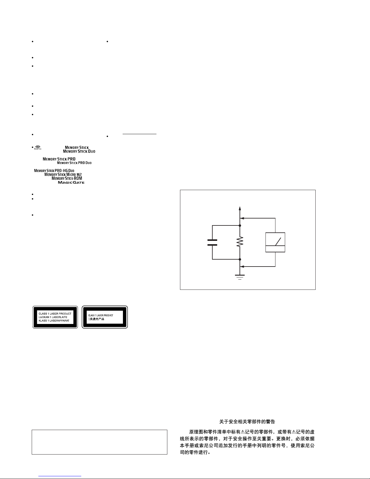
iPod models
You can use the following iPod models on this system. Update your iPod with the latest
soware before using it.
iPod nano
5th generation
(video camera)
iPod touch
2nd generation
iPod classic
120 GB
160 GB (2009)
iPod nano
4th generation
(video)
iPod classic
160 GB (2007)
iPod touch
1st generation
iPod nano
3rd generation
(video)
iPod classic
80 GB
iPod nano
2nd generation
(aluminum)
Design and specications are subject to
change without notice.
Outputs
DVD VIDEO OUT:
max. output level 1 Vp-p, unbalanced,
Sync negative, load impedance 75
PHONES:
accepts headphones of 8 or more
SPEAKERS:
Use only the supplied speakers
SS-SLK2i (WHG-SLK2i) or SS-SLK1i
(WHG-SLK1i).
AM tuner section
Tuning range
European and Saudi Arabian models:
531 kHz
1,602 kHz (9 kHz step)
North American and Latin American
models:
530 kHz
1,710 kHz (10 kHz step)
531 kHz
1,710 kHz (9 kHz step)
Other models:
531 kHz
1,602 kHz (9 kHz step)
530 kHz
1,610 kHz (10 kHz step)
Antenna:
AM loop antenna
Antenna terminals:
External antenna terminal
Intermediate frequency:
450 kHz
Inputs
VIDEO/SAT VIDEO IN:
1 Vp-p, 75
VIDEO/SAT AUDIO IN:
voltage 250/450 mV, impedance
47 k
Antenna:
FM lead antenna
Antenna terminals:
75 Ω unbalanced
Intermediate frequency:
10.7 MHz
HCD-SLK1i/SLK2i
SPECIFICATIONS
DVD RECEIVER
9-889-894-01
2010F05-1
©
2010.06
US Model
Canadian Model
AEP Model
Chinese Model
Saudi Arabia Model
Singapore Model
Korean Model
Thai Model
HCD-SLK1i
Mexican Model
Brazilian model
Argentina model
HCD-SLK2i
E Model
HCD-SLK1i/SLK2i
Ver. 1.0 2010.06
Model Name Using Similar Mechanism NEW
Mechanism Type CDM86B-DVBU101
Optical Pick-up Name KHM-313CAB
• HCD-SLK1i is the amplifi er, USB, memory card, disc player and tuner section in WHG-SLK1i.
• HCD-SLK2i is the amplifi er, USB, memory card, disc player and tuner section in WHG-SLK2i.
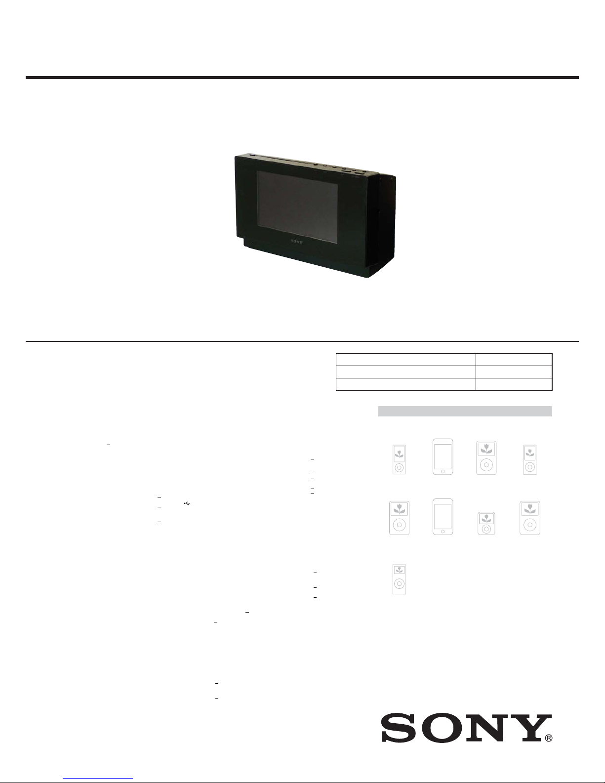
Photo: HCD-SLK1i
HCD-SLK1i/SLK2i
2
NOTES ON CHIP COMPONENT REPLACEMENT
• Never reuse a disconnected chip component.
• Notice that the minus side of a tantalum capacitor may be damaged by heat.
FLEXIBLE CIRCUIT BOARD REPAIRING
• Keep the temperature of soldering iron around 270 °C during
repairing.
• Do not touch the soldering iron on the same conductor of the
circuit board (within 3 times).
• Be careful not to apply force on the conductor when soldering
or unsoldering.
SAFETY CHECK-OUT
After correcting the original service problem, perform the following safety check before releasing the set to the customer:
Check the antenna terminals, metal trim, “metallized” knobs,
screws, and all other exposed metal parts for AC leakage.
Check leakage as described below.
LEAKAGE TEST
The AC leakage from any exposed metal part to earth ground and
from all exposed metal parts to any exposed metal part having a
return to chassis, must not exceed 0.5 mA (500 microamperes.).
Leakage current can be measured by any one of three methods.
1. A commercial leakage tester, such as the Simpson 229 or RCA
WT-540A. Follow the manufacturers’ instructions to use these
instruments.
2. A battery-operated AC milliammeter. The Data Precision 245
digital multimeter is suitable for this job.
3. Measuring the voltage drop across a resistor by means of a
VOM or battery-operated AC voltmeter. The “limit” indication
is 0.75 V, so analog meters must have an accurate low-voltage
scale. The Simpson 250 and Sanwa SH-63Trd are examples
of a passive VOM that is suitable. Nearly all battery operated
digital multimeters that have a 2 V AC range are suitable. (See
Fig. A)
1.5 kΩ0.15 μF
AC
voltmeter
(0.75 V)
To Exposed Metal
Parts on Set
Earth Ground
Fig. A. Using an AC voltmeter to check AC leakage.
SAFETY-RELATED COMPONENT WARNING!
COMPONENTS IDENTIFIED BY MARK 0 OR DOTTED LINE
WITH MARK 0 ON THE SCHEMATIC DIAGRAMS AND IN
THE PARTS LIST ARE CRITICAL TO SAFE OPERATION.
REPLACE THESE COMPONENTS WITH SONY PARTS
WHOSE PART NUMBERS APPEAR AS SHOWN IN THIS
MANUAL OR IN SUPPLEMENTS PUBLISHED BY SONY.
ATTENTION AU COMPOSANT AYANT RAPPORT
À LA SÉCURITÉ!
LES COMPOSANTS IDENTIFIÉS PAR UNE MARQUE 0 SUR
LES DIAGRAMMES SCHÉMATIQUES ET LA LISTE DES
PIÈCES SONT CRITIQUES POUR LA SÉCURITÉ DE FONCTIONNEMENT. NE REMPLACER CES COMPOSANTS QUE
PAR DES PIÈCES SONY DONT LES NUMÉROS SONT DONNÉS DANS CE MANUEL OU DANS LES SUPPLÉMENTS
PUBLIÉS PAR SONY.
CAUTION
Use of controls or adjustments or performance of procedures
other than those specifi ed herein may result in hazardous radia-
tion exposure.
THIS PRODUCT IS LICENSED UNDER
THE MPEG-4 VISUAL PATENT
PORTFOLIO LICENSE FOR THE
PERSONAL AND NON-COMMERCIAL
USE OF A CONSUMER FOR
(i) ENCODING VIDEO IN COMPLIANCE
WITH THE MPEG-4 VISUAL STANDARD
(“MPEG-4 VIDEO”)
AND/OR
(ii) DECODING MPEG-4 VIDEO THAT
WAS ENCODED BY A CONSUMER
ENGAGED IN A PERSONAL AND NONCOMMERCIAL ACTIVITY AND/OR WAS
OBTAINED FROM A VIDEO PROVIDER
LICENSED BY MPEG LA TO PROVIDE
MPEG-4 VIDEO.
NO LICENSE IS GRANTED OR SHALL
BE IMPLIED FOR ANY OTHER
USE. ADDITIONAL INFORMATION
INCLUDING THAT RELATING TO
PROMOTIONAL, INTERNAL AND
COMMERCIAL USES AND LICENSING
MAY BE OBTAINED FROM MPEG LA,
LLC. SEE http://www.mpegla.com/
All other trademarks and registered
trademarks are of their respective holders.
In this manual,
TM
and ® marks are not
specied.
Manufactured under license from Dolby
Laboratories. “Dolby” and the doubleD symbol are trademarks of Dolby
Laboratories.
“DVD+RW,” “DVD-RW,” “DVD+R,” “DVD
VIDEO,” and the “CD” logos are trademarks.
DivX® is a video le compression
technology, developed by DivX, Inc. DivX,
DivX Certied, and associated logos are
trademarks of DivX, Inc. and are used under
license.
is product is an ocial DivX
®
certied
product.
MPEG Layer-3 audio coding technology and
patents licensed from Fraunhofer IIS and
omson.
iPod is a trademark of Apple Inc., registered
in the U.S. and other countries.
“Made for iPod” means that an electronic
accessory has been designed to connect
specically to iPod and has been certied by
the developer to meet Apple performance
standards.
Apple is not responsible for the operation of
this device or its compliance with safety and
regulatory standards.
, “Memory Stick,” ,
“Memory Stick Duo,”
,
“MagicGate Memory Stick,” “Memory Stick
PRO,”
, “Memory
Stick PRO Duo,”
,
“Memory Stick PRO-HG Duo,”
, “Memory Stick
Micro,”
, , “Memory
Stick-ROM,”
,
“MagicGate,” and
are
trademarks or registered trademarks of Sony
Corporation.
SDHC Logo is a trademark of SD-3C, LLC.
Windows Media is either a registered
trademark or trademark of Microso
Corporation in the United States and/or
other countries.
is product is protected by certain
intellectual property rights of Microso
Corporation. Use or distribution of such
technology outside of this product is
prohibited without a license from Microso
or an authorized Microso subsidiary.
is appliance is classied as a CLASS 1
LASER product. is marking is located
on the rear exterior.

HCD-SLK1i/SLK2i
3
1. SERVICING NOTES ............................................. 4
2. DISASSEMBLY
2-1. Disassembly Flow ........................................................... 9
2-2. Top Panel Block .............................................................. 10
2-3. Rear Case Block .............................................................. 10
2-4. Main Chassis Block ........................................................ 11
2-5. MAIN Board ................................................................... 12
2-6. Switching Regulator Block ............................................. 12
2-7. Cover (CDM) Block ....................................................... 13
2-8. DVD Mechanism Deck Block ........................................ 13
2-9. DISPLAY Board ............................................................. 14
2-10. Optical Pick-up Block (KHM-313CAB) ........................ 15
2-11. Belt (MOT) ..................................................................... 15
2-12. LCD Board ...................................................................... 16
2-13. LCD Module ................................................................... 16
3. TEST MODE ............................................................ 17
4. DIAGRAMS
4-1. Block Diagram - SERVO Section - ................................ 21
4-2. Block Diagram - AUDIO INPUT Section - .................... 22
4-3. Block Diagram - AUDIO OUTPUT Section - ................ 23
4-4. Block Diagram - VIDEO Section - ................................. 24
4-5. Block Diagram
- PANEL, POWER SUPPLY Section - ........................... 25
4-6. Schematic Diagram - DISPLAY Section (1/7) - ............. 27
4-7. Schematic Diagram - DISPLAY Section (2/7) - ............. 28
4-8. Schematic Diagram - DISPLAY Section (3/7) - ............. 29
4-9. Schematic Diagram - DISPLAY Section (4/7) - ............. 30
4-10. Schematic Diagram - DISPLAY Section (5/7) - ............. 31
4-11. Schematic Diagram - DISPLAY Section (6/7) - ............. 32
4-12. Schematic Diagram - DISPLAY Section (7/7) - ............. 33
4-13. Printed Wiring Board - DISPLAY Section (1/2) - .......... 34
4-14. Printed Wiring Boards - DISPLAY Section (2/2) - ......... 35
TABLE OF CONTENTS
4-15. Printed Wiring Board - LCD Board - .............................. 36
4-16. Schematic Diagram - LCD Board - ................................ 37
4-17. Printed Wiring Boards - AUDIO IN/OUT Section - ....... 38
4-18. Schematic Diagram - AUDIO IN/OUT Section - ........... 39
4-19. Printed Wiring Boards - KEY Section - .......................... 40
4-20. Schematic Diagram - KEY Section - .............................. 41
4-21. Printed Wiring Board
- MAIN Board (Component Side) (SUFFIX-11) - ......... 42
4-22. Printed Wiring Board
- MAIN Board (Conductor Side) (SUFFIX-11) - ........... 43
4-23. Printed Wiring Board
- MAIN Board (Component Side) (SUFFIX-12) - ......... 44
4-24. Printed Wiring Board
- MAIN Board (Conductor Side) (SUFFIX-12) - ........... 45
4-25. Schematic Diagram - MAIN Board (1/4) - ..................... 46
4-26. Schematic Diagram - MAIN Board (2/4) - ..................... 47
4-27. Schematic Diagram - MAIN Board (3/4) - ..................... 48
4-28. Schematic Diagram - MAIN Board (4/4) - ..................... 49
5. EXPLODED VIEWS
5-1. Top Panel, Rear Case Section ......................................... 64
5-2. Switching Regulator Section .......................................... 65
5-3. MAIN Board Section ...................................................... 66
5-4. DISPLAY Board Section ................................................ 67
5-5. Front Panel Section ......................................................... 68
5-6. DVD Mechanism Deck Section
(CDM86B-DVBU101) ................................................... 69
6. ELECTRICAL PARTS LIST .............................. 70
Accessories are given in the last of the electrical parts list.
Note: Refer to the servicing notes “MAIN BOARD
DISCRIMINATION” (page 4) for how to
distinguish SUFFIX-11 and SUFFIX-12.
HCD-SLK1i/SLK2i
4
SECTION 1
SERVICING NOTES
NOTES ON HANDLING THE OPTICAL PICK-UP
BLOCK OR BASE UNIT
The laser diode in the optical pick-up block may suffer electrostatic break-down because of the potential difference generated by
the charged electrostatic load, etc. on clothing and the human body.
During repair, pay attention to electrostatic break-down and also
use the procedure in the printed matter which is included in the
repair parts.
The fl exible board is easily damaged and should be handled with
care.
NOTES ON LASER DIODE EMISSION CHECK
The laser beam on this model is concentrated so as to be focused
on the disc refl ective surface by the objective lens in the optical
pickup block. Therefore, when checking the laser diode emission,
observe from more than 30 cm away from the objective lens.
UNLEADED SOLDER
Boards requiring use of unleaded solder are printed with the leadfree mark (LF) indicating the solder contains no lead.
(Caution: Some printed circuit boards may not come printed with
the lead free mark due to their particular size)
: LEAD FREE MARK
Unleaded solder has the following characteristics.
• Unleaded solder melts at a temperature about 40 °C higher
than ordinary solder.
Ordinary soldering irons can be used but the iron tip has to be
applied to the solder joint for a slightly longer time.
Soldering irons using a temperature regulator should be set to
about 350 °C.
Caution: The printed pattern (copper foil) may peel away if
the heated tip is applied for too long, so be careful!
• Strong viscosity
Unleaded solder is more viscous (sticky, less prone to fl ow)
than ordinary solder so use caution not to let solder bridges
occur such as on IC pins, etc.
• Usable with ordinary solder
It is best to use only unleaded solder but unleaded solder may
also be added to ordinary solder.
RELEASING THE DISC SLOT LOCK
The disc slot lock function for the antitheft of an demonstration
disc in the store is equipped.
Releasing Procedure:
1. Press the [
?/1
] button to turn on the system.
2. Touch the [HOME] sensor.
3. Touch the [M], [m], [<] and [,] sensors to select the “CD/
DVD”, and touch the [ENTER] sensor.
4. Press two buttons of [x] and [Z] simultaneously, and hold for
more than fi ve seconds.
5. The message “UNLOCKED” is displayed on the liquid crystal
display module and the disc slot is unlocked.
Note: When “LOCKED” is displayed, the disc slot lock is not released by
turning power on/off with the [
?/1
] button.
NOTE FOR REPLACEMENT OF THE MS-214 BOARD
When the MS-214 board is defective, exchange the entire MD
(AU) ASSY.
NOTE FOR REPLACEMENT OF THE TOUCH PANEL
BOARD
When the TOUCH PANEL board is defective, exchange the entire
mounted board.
MODEL IDENTIFICATION
– Bottom view –
Model
Number
Label
Model Part No.
SLK1i: US model
Model number label is
marked on the panel.
SLK1i: 240V AC area in E model
4-189-097-0[]
SLK2i: 240V AC area in E model
4-189-097-1[]
SLK1i: Singapore model
4-189-098-0[]
SLK1i: Canadian model
4-189-100-0[]
SLK1i: AEP model
4-189-102-0[]
SLK1i: Saudi Arabia model
4-189-103-0[]
SLK1i: Korean model
4-189-104-0[]
SLK2i: 120V AC area in E, Chilean
and Peruvian models
4-189-105-0[]
SLK2i: Brazilian model
4-189-106-0[]
SLK2i: Argentina model
4-189-107-0[]
SLK2i: Mexican model
4-189-108-0[]
SLK1i: Thai model
4-189-309-0[]
SLK1i: Chinese model
4-191-613-0[]
MAIN BOARD DISCRIMINATION
In this set, the MAIN board has been changed in the midway of
production.
Repair after distinguishing each type set to doing the repair referring to the following.
– MAIN Board (Component Side) –
SUFFIX-11 : 1-881-738-11
SUFFIX-12 : 1-881-738-12
HCD-SLK1i/SLK2i
5
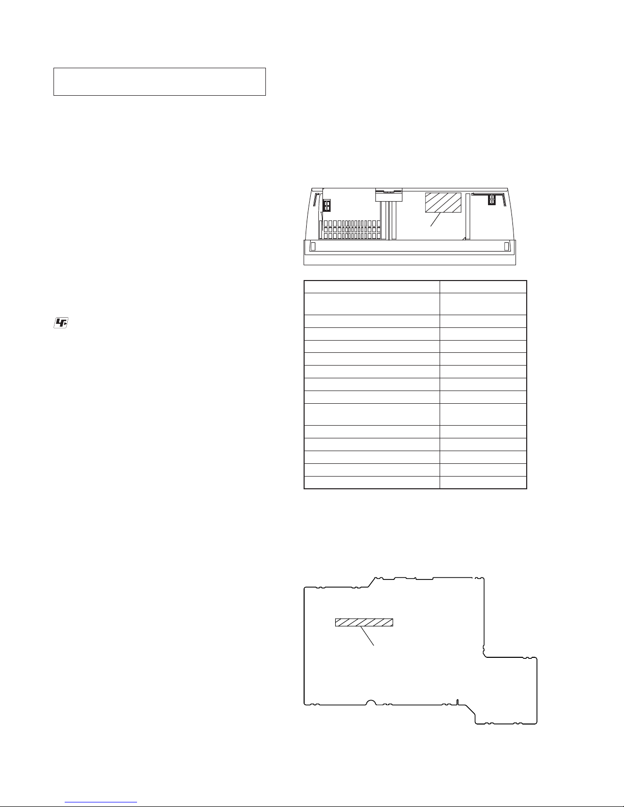
CAPACITOR ELECTRICAL DISCHARGE PROCESSING
When checking the board, the electrical discharge is necessary for
the electric shock prevention.
Connect the resistors referring to the fi gure below.
• Switching regulator (C201, C202) (for HCD-SLK1i)
Both ends of respective capacitors.
– Switching Regulator (Conductor Side) –
T101
C202
C201
800 :/2 W
800 :/2 W
• Switching regulator (C201) (for HCD-SLK2i)
Both ends of respective capacitor.
– Switching Regulator (Conductor Side) –
T101
C201
800 :/2 W

HCD-SLK1i/SLK2i
6
HOW TO EJECT THE DISC WHEN POWER SWITCH TURNS OFF
Note: Please take out the DVD mechanism block from a set referring to “SECTION 2 DISASSEMBLY”.
IP BOARD SERVICE POSITION
Please rotate the pully in the direction of the arrow after removing mechanism deck,
and eject the disc.
disc
– DVD mechanism block bottom view –
DISPLAY board
IP board
wire from switching regulator fan cable
fan motor
Note: Neither the wire from switching regulator
nor the fan cable must loosen.
HCD-SLK1i/SLK2i
7
MAIN BOARD SERVICE POSITION
• Please connect following extension jig.
Jig No. Part No. Pitch (mm) Cores Length (mm)
1
J-2501-102-A 1 13 300
DISPLAY board
MAIN board
TERMINAL board
Connect extension jig 1
to the MAIN board (CN101) and DISPLAY board (CN408)
Connect extension jig 1
to the MAIN board (CN301) and DISPLAY board (CN302)
CN101
CN302
CN408
CN301
Note:
Please do not make a mistake when you install the extention jig
because CN101 and CN301 on MAIN board and CN302 and
CN408 on DISPLAY board are all thirteen pins.
SWITCHING REGULATOR SERVICE POSITION
• Please connect following extension jig.
Jig No. Part No. Pitch (mm) Cores Length (mm)
1
J-2501-102-A 1 13 300
DISPLAY board
SWITCHING REGULATOR
MAIN board
TERMINAL board
Connect extension jig 1
to the MAIN board (CN101) and DISPLAY board (CN408)
Connect extension jig 1
to the MAIN board (CN301) and DISPLAY board (CN302)
CN101
CN302
CN408
CN301
Note:
Please do not make a mistake when you install the extention jig
because CN101 and CN301 on MAIN board and CN302 and
CN408 on DISPLAY board are all thirteen pins.
HCD-SLK1i/SLK2i
8
DISPLAY BOARD SERVICE POSITION
• Please connect following extension jig.
Jig No. Part No. Pitch (mm) Cores Length (mm)
1
J-2501-102-A 1 13 300
2
J-2501-245-A 1 23 300
3
J-2501-248-A 1 27 300
DVD MECHANISM DECK, LCD AND JACK BOARDS SERVICE POSITION
• Please connect following extension jig.
Jig No. Part No. Pitch (mm) Cores Length (mm)
1
J-2501-102-A 1 13 300
2
J-2501-245-A 1 23 300
3
J-2501-248-A 1 27 300
4
J-2501-241-A 1 7 300
TERMINAL board
DISPLAY board
LCD board
MAIN board
Connect extension jig 1
to the MAIN board (CN101)
and DISPLAY board (CN408)
Connect extension jig 1
to the MAIN board (CN301)
and DISPLAY board (CN302)
Connect extension jig 2
to the DISPLAY board (CN407)
and LCD board (CN904)
Connect extension jig 3
to the DISPLAY board (CN406)
and LCD board (CN903)
CN101
CN302
CN408
CN301
CN407
CN904
CN903
CN406
Note:
Please do not make a mistake when you
install the extention jig because CN101
and CN301 on MAIN board and CN302
and CN408 on DISPLAY board are all
thirteen pins.
SWITCHING REGULATOR block
DISPLAY board
DVD mechanism deck
LCD board
MAIN board
Connect extension jig 1
to the MAIN board (CN101)
and DISPLAY board (CN408)
Connect extension jig 4
to the JACKboard (CN705)
and DISPLAY board (CN604)
Connect extension jig 1
to the MAIN board (CN301)
and DISPLAY board (CN302)
Connect extension jig 2
to the DISPLAY board (CN407)
and LCD board (CN904)
Connect extension jig 3
to the DISPLAY board (CN406)
and LCD board (CN903)
CN101
CN302
CN705
CN408
CN604
CN301
CN407
CN904
CN903
CN406
Note:
Please do not make a mistake when you
install the extention jig because CN101
and CN301 on MAIN board and CN302
and CN408 on DISPLAY board are all
thirteen pins.
SWITCHING REGULATOR block
TERMINAL board
JACK board
HCD-SLK1i/SLK2i
9
SECTION 2
DISASSEMBLY
• This set can be disassembled in the order shown below.
2-1. DISASSEMBLY FLOW
SET
2-2. TOP PANEL BLOCK
(Page 10)
2-3. REAR CASE BLOCK
(Page 10)
2-4. MAIN CHASSIS BLOCK
(Page 11)
2-6. SWITCHING REGULATOR BLOCK
(Page 12)
2-7. COVER (CDM) BLOCK
(Page 13)
2-8. DVD MECHANISM DECK BLOCK
(Page 13)
2-10. OPTICAL PICK-UP BLOCK
(KHM-313CAB)
(Page 15)
2-9. DISPLAY BOARD
(Page 14)
2-11. BELT (MOT)
(Page 15)
2-12. LCD BOARD
(Page 16)
2-5. MAIN BOARD
(Page 12)
2-13. LCD MODULE
(Page 16)
HCD-SLK1i/SLK2i
10
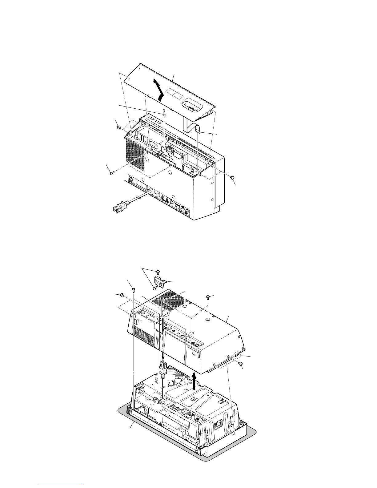
2-3. REAR CASE BLOCK
sheet
Note: Please spread a sheet under a set
not to injure front panel.
– Rear bottom view –
1
two flat head screws
(TP)
2
support (bushing)
7
8
4
four screws
(SLK1i: BTT4 u 8/SLK2i: hook)
5
four screws
(BVTP2.6)
3
two flat head screws
(TP)
3
two flat head screws
(TP)
6
claw
9
rear case block
6
claw
Note: Follow the disassembly procedure in the numerical order given.
2-2. TOP PANEL BLOCK
4
wire (flat type) (11 core)
(CN404)
5
connector
(CN405)
6
top panel block
1
two flat head screws
(TP)
2
two flat head screws
(TP)
3
2
two flat head screws
(TP)
– Rear view –
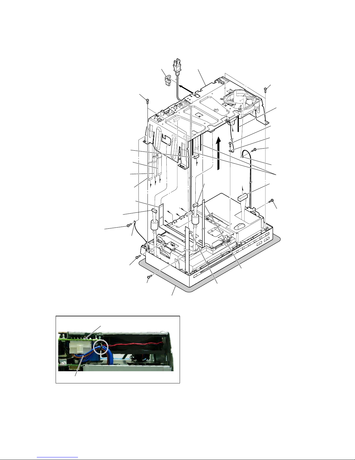
HCD-SLK1i/SLK2i
11
2-4. MAIN CHASSIS BLOCK
A
A
B
C
D
E
B
C
D
E
sheet
– Rear top view –
qd
screw
(BVTP3 u 8)
qd
screw
(BVTP3 u 8)
qd
screw
(BVTP3 u 8)
qd
screw
(BVTP3 u 8)
qh
two screws
(BVTP2.6)
qh
two screws
(BVTP2.6)
qh
screw (BVTP2.6)
qd
screw
(BVTP3 u 8)
qf
wire (GND)
qg
wire
qj
wire
qk
2
cord bushing
1
qs
wire (flat type) (13 core)
(CN302)
ql
wire (flat type) (15 core)
(CN102)
qa
wire (flat type) (7 core)
(CN604)
4
connector
(CN900)
9
connector
(CN602)
w;
connector
(CN304)
wa
main chassis block
6
connector
(CN901)
3
Lift up the lead pin.
5
Lift up two lead pins.
0
wire (flat type) (13 core)
(CN408)
7
wire (flat type) (11 core)
(CN104)
8
wire (flat type) (13 core)
(CN103)
Note 1:
Please spread a sheet under a set
not to injure front panel.
Note 2:
Please do not make a mistake when you
install the wire (flat type) (13 core)
because CN302 and CN408 are both
thirteen pins.
wire from switching regulator
:ire VettiQJ
MAIN board
HCD-SLK1i/SLK2i
12
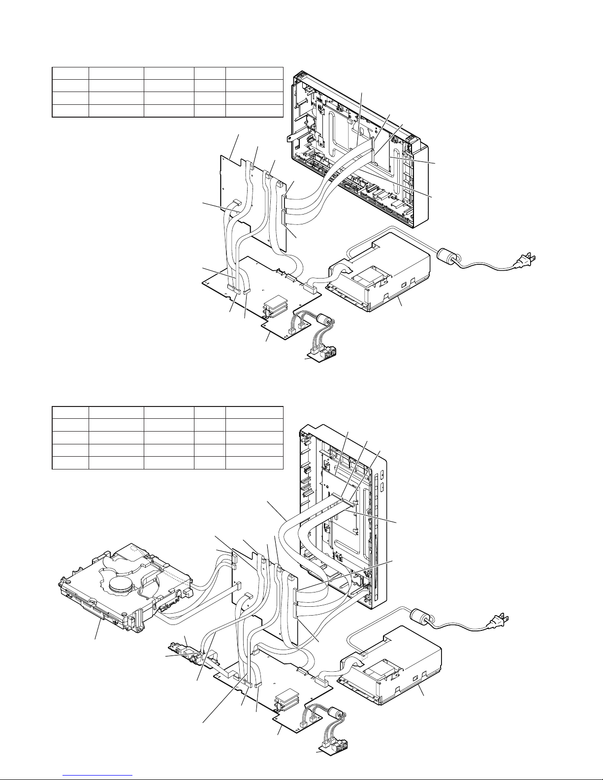
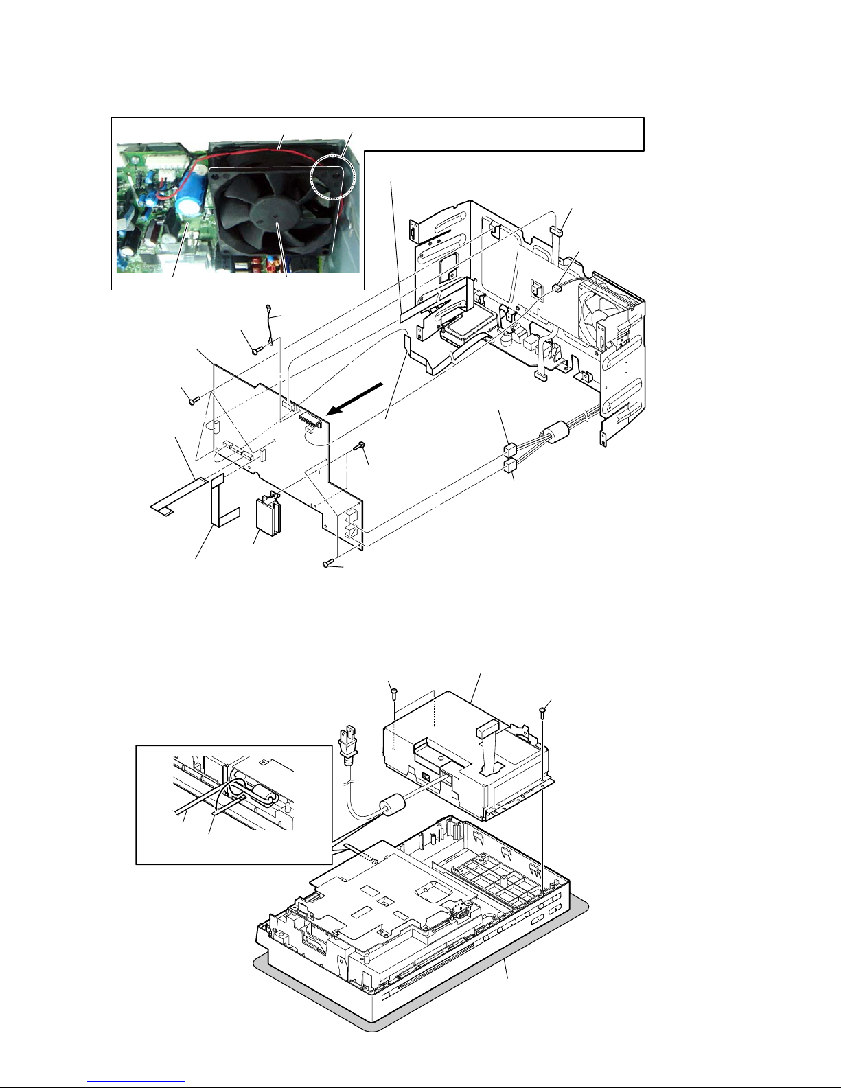
2-5. MAIN BOARD
2-6. SWITCHING REGULATOR BLOCK
5
wire (flat type) (11 core) (CN302) (AEP)/
wire (flat type) (9 core) (CN303) (except AEP)
qa
wire (flat type) (13 core)
(CN301)
0
wire (flat type) (13 core)
(CN101)
4
wire (flat type) (9 core)
(CN105)
1
DC fan connector
(CN600)
2
connector
(CN601)
6
connector
(CN902)
3
connector
(CN602)
7
three screws
(BVTP3 u 8)
qs
three screws
(BVTP3 u 8)
qd
heat sink (AMP)
qf
MAIN board
9
7
three screws
(BVTP3 u 8)
7
screw
(BVTP3 u 8)
8
wire
:LUHVHWWLQJ
MAIN board
fan cable
fan motor
Note 2:
Please do not make a mistake when you install the
wire (flat type) (13 core) because CN101 and CN301
are both thirteen pins.
Note 1:
Please let me crawl the side of the fan motor about the cable
because the cable is drawn in to the fan motor.
sheet
– Rear top view –
2
two screws
(BVTP2.6)
1
Release the power cord
flom the coating clip.
power cord
2
two screws
(BVTP2.6)
3
switching regulator block
Note: Please spread a sheet under a set
not to injure front panel.
HCD-SLK1i/SLK2i
13
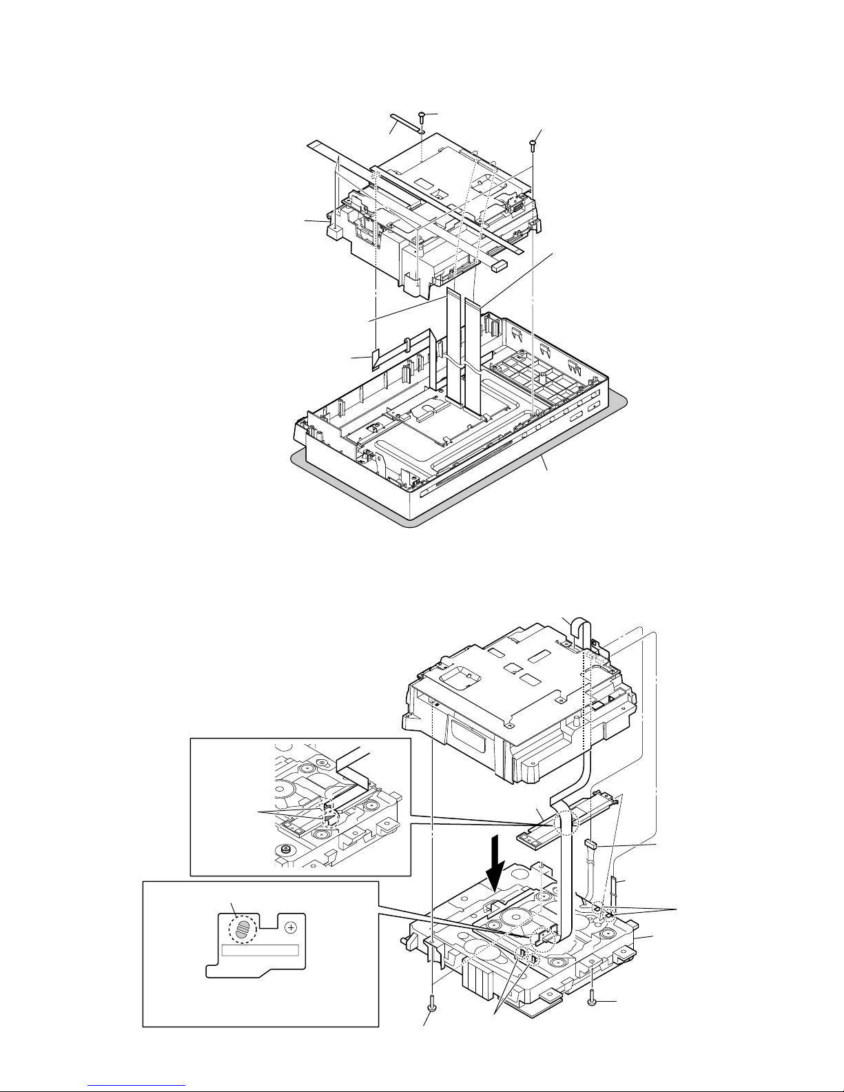
2-7. COVER (CDM) BLOCK
2-8. DVD MECHANISM DECK BLOCK
Note 1: When disconnecting the wire (fl at type) (24 core) of optical pick-up block, solder the short-land.
4 four screws
(BVTP2.6)
4 screw
(BVTP2.6)
5 coating clip
6 cover (CDM) block
1
wire (flat type) (11 core)
(CN412)
2
wire (flat type) (27 core)
(CN406)
3
wire (flat type) (23 core)
(CN407)
sheet
– Rear top view –
Note: Please spread a sheet under a set
not to injure front panel.
8
Solder the short-land.
Note 2: When assembling the optical pick-up block,
remove the solder of short-land after
connecting the wire (flat type) (24 core).
7 FFC holder
4
6 two claws
6 two claws
0 DVD mechanism
deck block
1 wire (flat type) (7 core)
(CN201)
9 wire (flat type) (24 core)
(CN001)
2 connector
(CN202)
3 two screws
(BVTP2.6)
3 screw
(BVTP2.6)
– DVD mechanism deck block bottom view –
5 two claws
HCD-SLK1i/SLK2i
14
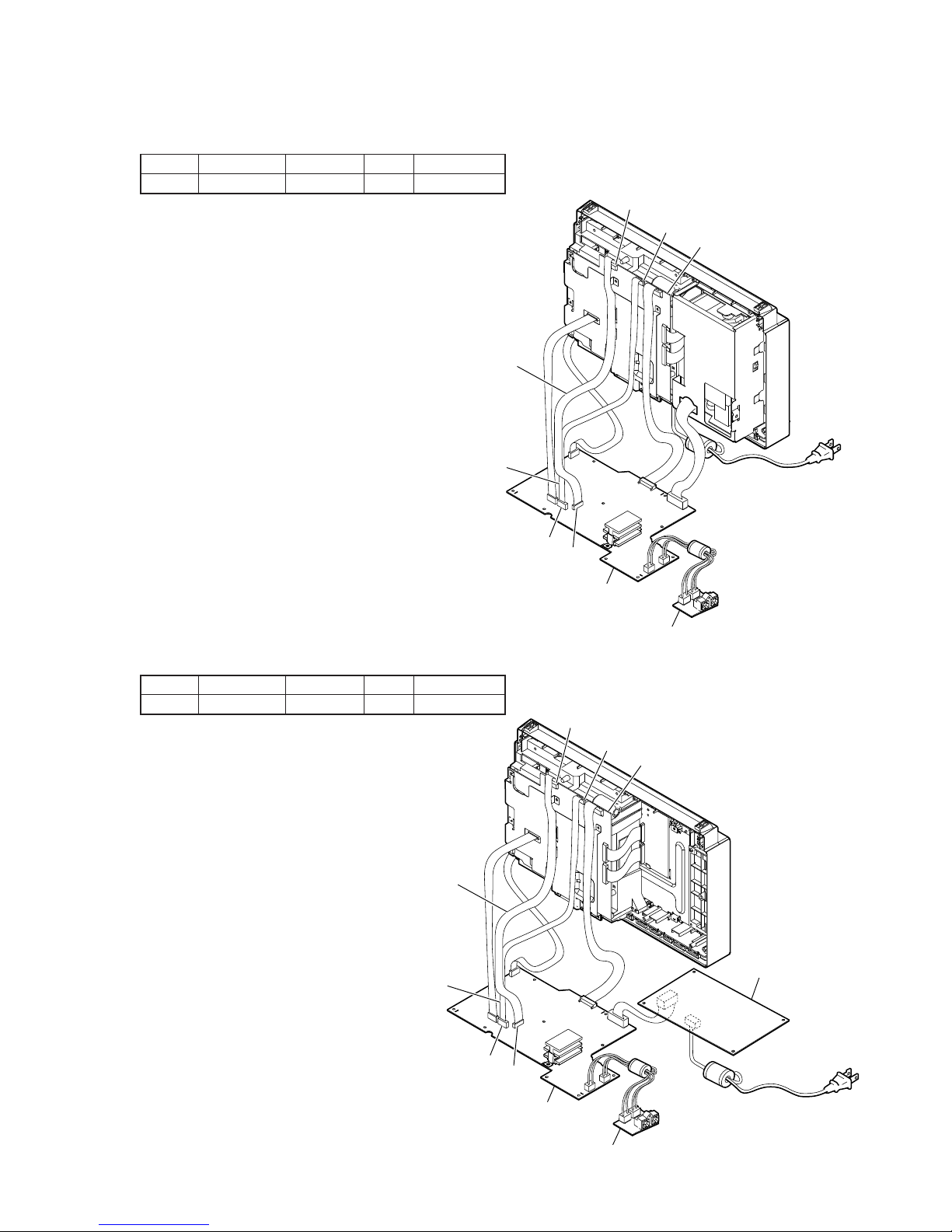
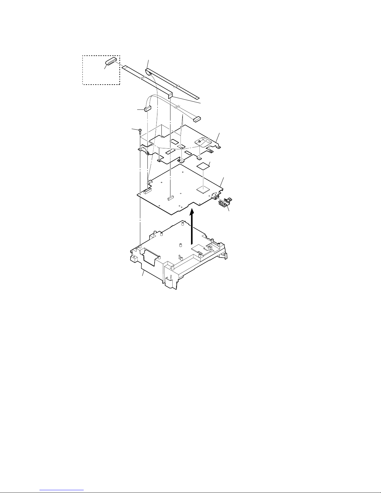
2-9. DISPLAY BOARD
(US, Canadian)
5 eight screws
(BVTP2.6)
3
wire (flat type) (15 core)
(CN002)
1
connector
(CN301)
2
ferrite core
6 shield (MS)
9 ground plate (USB)
8 cover (CDM)
0 radiation sheet
qa DISPLAY board
7
4
wire (flat type) (11 core)
(CN411)
HCD-SLK1i/SLK2i
15
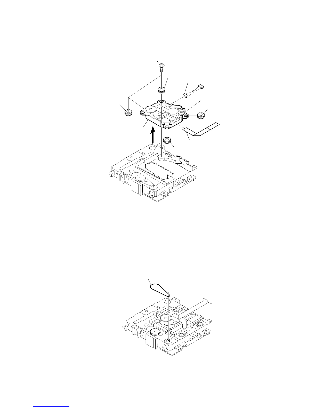
2-10. OPTICAL PICK-UP BLOCK (KHM-313CAB)
2-11. BELT (MOT)
– DVD mechanism deck block bottom view –
1
four insulator screws
2
5
insulator
3
connector
4
wire (flat type) (24 core)
6
optical pick-up block
(KHM-313CAB)
5
insulator
5
insulator
5
insulator
– DVD mechanism deck block bottom view –
1 belt (MOT)
HCD-SLK1i/SLK2i
16
2-12. LCD BOARD
2-13. LCD MODULE
sheet
Note: Please spread a sheet under a set
not to injure front panel.
4 two screws
(BVTP2.6)
5 two claw
s
1 LCD module connector
(CN905)
2 LCD module flexible flat cable
(CN901)
3 LCD module flexible flat cable
(CN902)
6
7
wire (flat type) (27 core)
(CN903)
8
wire (flat type) (23 core)
(CN904)
9
LCD board
– Rear bottom view –
sheet
Note: Please spread a sheet under a set
not to injure front panel.
– Rear bottom view –
2 three screws
(BVTP2.6)
6 four screws
(BVTP2.6)
7 ground plate (LCD)
8 wire (GND)
9 bracket (LCD)
6 two screws
(BVTP2.6)
5 ornament (CDM) assy
3
1
wire (flat type) (11 core)
(KEY-RIGHT board: CN263, KEY-LEFT board: CN262)
4 two bosses
qa LCD module
0
HCD-SLK1i/SLK2i
17
SECTION 3
TEST MODE
COLD RESET
Reset the system to its factory default settings.
Procedure:
1. Press the [
?/1
] button to turn on the system.
2. Touch the [M], [m], [<] and [,] sensors to select the “Settings”, and touch the [ENTER] sensor.
3. Touch the [M], [m], [<] and [,] sensors to select the “Reset
all settings”, and touch the [ENTER] sensor.
4. Touch the [<] and [,] sensors to select the “Yes”, and touch
the [ENTER] sensor.
5. All the settings are reset and returned to the default settings,
then become standby mode.
VERSION DISPLAY
Each version, destination and model name are displayed.
Procedure:
1. Press the [
?/1
] button to turn on the system.
2. Press two buttons of [x] and [VOL –] and touch the [OPTIONS] sensor simultaneously.
3. The system version, GUI version, DVD version, destination
and model name are displayed on the liquid crystal display
module.
• Screen display
Settings
System Information
System
GUI
DVD
Dest.
Model
:
:
:
:
:
1
2
3
4
5
Software version
1 System version
2 GUI version
3 DVD version
4 Destination:
00: Singapore or Thai model
02: 240V AC area in E model
04: Saudi Arabia model
09: Brazilian model
10: US or Canadian model
11: Korean model
12: 120V AC area in E, Chilean, Peruvian or Argentina model
13: Mexican model
14: Chinese model
16: AEP model
5 Model name:
00: HCD-SLK1i
16: HCD-SLK2i
Releasing method:
Press the [
?/1
] button to turn off the system.
COMMON TEST
The test of each category is executed.
Procedure:
1. Press the [
?/1
] button to turn on the system.
2. Press two buttons of [x] and [VOL –] and touch the [ENTER]
sensor simultaneously, then become common test mode.
3. When the [VOL +] button is pressed, the sound volume increases to its maximum and the message “Max.” appears on
the liquid crystal display module.
4. When the [VOL –] button is pressed, the sound volume decreases to its minimum and the message “Min.” appears on the
liquid crystal display module.
Releasing method:
Press the [
?/1
] button to turn off the system.
VACS DISPLAY
The test of each category is executed.
Procedure:
1. Press the [
?/1
] button to turn on the system.
2. Press two buttons of [x] and [VOL +] and touch the [ENTER]
sensor simultaneously.
3. The [AUTO STANDBY] indicator repeats on and off, then become VACS display mode.
4. Press two buttons of [x] and [>] buttons and touch the [ENTER] sensor simultaneously.
5. The [AUTO STANDBY] indicator blinks corresponding to the
VACS level at that time.
Blinking frequency: VACS level (0 to 5).
Releasing method:
Press two buttons of [x] and [VOL +] buttons and touch the [ENTER] sensor simultaneously.
DVD SHIP MODE AND COLD RESET
Cold reset is executed at the same time with DVD ship
mode.
Procedure:
1. Press the [
?/1
] button to turn on the system.
2. Touch the [HOME] sensor.
3. Touch the [M], [m], [<] and [,] sensors to select the “CD/
DVD”, and touch the [ENTER] sensor.
4. Conrm there is no disc in the disc slot.
5. Press three buttons [x], [.] and [
[/1
] simultaneously.
6. Become standby mode, then become DVD ship mode.
Releasing method:
Pull out the power code.
VIDEO/SAT CHANGE
This mode changes external video source.
Procedure:
1. Press the [
?/1
] button to turn on the system.
2. Touch the [M], [m], [<] and [,] sensors to select the “Settings”, and touch the [ENTER] sensor.
3. Touch the [M], [m], [<] and [,] sensors to select the “External Video Source”, and touch the [ENTER] sensor.
4. Touch the [M] and [m] sensors to select the “Video” or “Satellite”, and touch the [ENTER] sensor.
5. The external video source changed.
HCD-SLK1i/SLK2i
18
DISC ANTITHEFT LOCK
This mode is used to unable to take sample disc out of disc slot in
the shop.
Procedure:
1. Press the [
?/1
] button to turn on the system.
2. Touch the [HOME] sensor.
3. Touch the [M], [m], [<] and [,] sensors to select the “CD/
DVD”, and touch the [ENTER] sensor.
4. Press two buttons of [x] and [Z] simultaneously, and hold for
more than ve seconds.
5. The message “LOCKED” is displayed on the liquid crystal
display module and the disc slot is locked (Even if pressing the
[Z] button, the message “LOCKED” is displayed on the liquid
crystal display module and the disc slot is locked).
Releasing method:
1. Press two buttons of [x] and [Z] buttons simultaneously, and
hold for more than ve seconds.
2. The message “UNLOCKED” is displayed on the liquid crystal
display module and the disc slot is unlocked.
DVD COLOR SYSTEM CHANGE (SLK1i: 240V AC area
in E, Saudi Arabia, Singapore, Korean, Thai, Chinese/
SLK2i: 120V AC area in E and 240V AC area in E models
only)
This mode let you change the color system of the video output
from PAL to NTSC or vice-versa.
Procedure:
1. Press the [
?/1
] button to turn on the system.
2. Touch the [HOME] sensor.
3. Touch the [M], [m], [<] and [,] sensors to select the “CD/
DVD”, and touch the [ENTER] sensor.
4. Press the [
?/1
] button to turn off the system.
5. Press two buttons of [X] and [
?/1
] simultaneously.
6. The message “DVD COLOR NTSC” or “DVD COLOR PAL”
displayed on the liquid crystal display module and thus the
color system is changed.
MTK REBOOT PREVENT
This mode is setting that MTK is not rebooted.
Procedure:
1. Press the [
?/1
] button to turn on the system.
2. Touch the [HOME] sensor.
3. Touch the [M], [m], [<] and [,] sensors to select the “CD/
DVD”, and touch the [ENTER] sensor.
4. Press three buttons [x], [>] and [Z] simultaneously.
5. The rebooting prevention setting was completed (there is no
change in the display).
Releasing method:
Press the [
?/1
] button to turn off the system.
TUNER STEP CHANGE (SLK1i: US, Canadian, 240V AC
area in E, Singapore, Korean, Thai, Chinese/SLK2i only)
The step interval of AM channels can be toggled between 9 kHz
and 10 kHz.
Procedure:
1. Press the [
?/1
] button to turn on the system.
2. Touch the [M], [m], [<] and [,] sensors to select the “Settings”, and touch the [ENTER] sensor.
3. Touch the [M], [m], [<] and [,] sensors to select the “AM
Step Change”, and touch the [ENTER] sensor.
4. Touch the [M] and [m] sensors to select the “9kHz” or “10kHz”,
and touch the [ENTER] sensor.
5. The step interval of AM channels changed.
REMOTE DISABLE MODE
This mode disable the remote commander reception.
Procedure:
1. Press the [
?/1
] button to turn on the system.
2. Press two buttons [x] and [VOL +] and touch the [OPTIONS]
sensor simultaneously.
3. The remote commander reception is invalidated (there is no
change in the display).
Releasing method:
Press two buttons [x] and [VOL +] and touch the [OPTIONS]
sensor simultaneously.
DVD SECTION
GENERAL DESCRIPTION
The IOP measurement allows you to make diagnosis and adjustment simply by using the remote commander . The instructions,
diagnosis results, etc. are given on the on-screen display (OSD).
Be sure to execute the IOP measurement when a BU (Base Unit)
is replaced.
DVD SERVICE MODE
It changes to the DVD service mode. Remote commander is necessary for the operation.
1. HOW TO ENTER THE DVD SERVICE MODE
Procedure:
1. Press the [
?/1
] button to turn on the system.
2. Touch the [HOME] sensor.
3. Touch the [M], [m], [<] and [,] sensors to select the “CD/
DVD”, and touch the [ENTER] sensor.
4 Press three buttons of [x], [VOL +] and [Z] simultaneously.
5. The DVD service mode starts.
The menu shown below will be displayed on the liquid crystal
display module.
Re mo co n Dia gnosi s Men u
0. Exte rn al Ch ip Ch ec k
1. Serv o Par am eter Ch eck
2. Driv e Man ua l Ope ra tion
3. Emer ge ncy His tory
4. Vers io n Inf or mation
Mo de l N am e
EE PR OM NO CL EA R
IF -c on : Ve r. XX .X X (XX XX )
Sy sc on : Ver. X.XXX
: XXXXX XX X
6. The menu above is the Remocon Diagnosis Menu screen
which consists of ve main functions. At the bottom of the
menu screen, the model name, IF-con version and Syscon version.
Releasing method:
Press the [
?/1
] button to turn off the system.
HCD-SLK1i/SLK2i
19
1-1. EXECUTING IOP MEASUREMENT
In order to execute IOP measurement, the following standard procedures must be followed.
Procedure:
1. Enter the DVD service mode.
2. Select “2. Drive Manual Operation” by pressing the [2] button
on the remote commander. The screen will appear as shown.
Drive Manual Operation
1. Servo Control
2. Track/Layer Jump
3. Manual Adjustment
4. Tray Aging Mode
5. MIRR time Adjust
0. Return to Top Menu
3. Select “3. Manual Adjustment” by pressing the [3] button on
the remote commander. The screen will appear as shown.
Manual Adjust
1. Track Balance Adjust:
2. Track Gain Adjust:
3. Focus Balance Adjust:
4. Focus Gain Adjust:
5. Eq Boost Adjust:
6. Iop:
7. TRV. Level:
8. S curve(FE) Level:
9. RFL(PI) Level:
0. MIRR Time:
[ M ] [ m ] Change Value
[RETURN] Return to previous menu
4. Select “6. IOP” by pressing the [6] button on the remote commander.
5. Wait until a hexadecimal number appear.
Manual Adjust
1. Track Balance Adjust:
2. Track Gain Adjust:
3. Focus Balance Adjust:
4. Focus Gain Adjust:
5. Eq Boost Adjust:
6. Iop. 51:
7. TRV. Level:
8. S curve(FE) Level:
9. RFL(PI) Level:
0. MIRR Time:
[ M ] [ m ] Change Value
[RETURN] Return to previous menu
6. Convert each data from hexadecimal to decimal using conversion table.
7. Please fi nd the label on the rear of the BU (Base Unit).
The default IOP value is written in the label.
8. Subtract between these two values.
9. If the remainder is smaller than 93 (decimal), then it is OK.
However if the value is higher than 93, then the BU is defective and need to be change.
10. Press the [RETURN] button on the remote commander to return back to previous menu.
11. Press the [0] button on the remote commander to return to Top
Menu.
1-2. EMERGENCY HISTORY
To check the emergency history, please follow the following procedure.
Procedure:
1. From the Top Menu of Remocon Diagnosis Menu, select “3.
Emergency History Check” by pressing the [3] button on the
remote commander. The following screen appears on the onscreen display.
Emg. History Check
01. 01 05 04 04
Laser Hours CD 999h 59min
DVD 999h 59min
00 92 46 00
00 00 00 00 00 00 23 45
02. 02 02 01 01 00 A9 4B 00
00 00 00 00 00 00 23 45
[Next] Next Page [Prev] Prev Page
[O] Return to Top Menu
2. You can check the total time when the laser is turned on during
playback of DVD and CD from the above menu. The maximum time, which can be displayed are 999h 59min.
3. You can check the error code of latest 10 emergency history
from the above menu. To view the previous or next page of
emergency history, press [.] or [>] button on the remote
commander. The error code consists of the following three
blocks. The fi rst block indicates the error code. The second
block indicates the parameter and the third block indicates the
time of error code as shown below.
• Error Code
Emg. History Check
01. 01 05 04 04
Laser Hours CD 999h 59min
DVD 999h 59min
00 92 46 00
00 00 00 00 00 00 23 45
02. 02 02 01 01 00 A9 4B 00
00 00 00 00 00 00 23 45
[Next] Next Page [Prev] Prev Page
[O] Return to Top Menu
*1 *2
*3
*1 : Error Code
*2 : Parameter of error code
*3 : Time of error code
The meaning of error code is as below:
01: Communication error (No reply from syscon)
02: Syscon hung up
03: Power OFF request when syscon hung up
19: Thermal shutdown
24: MoveSledHome error
25: Mechanical move error (5 Changer)
26: Mechanical move stack error
30: DC motor adjustment error
31: DPD offset adjustment error
32: TE balance adjustment error
33: TE sensor adjustment error
34: TE loop gain adjustment error
35: FE loop gain adjustment error
36: Bad jitter after adjustment
40: Focus NG
42: Focus layer jump NG
HCD-SLK1i/SLK2i
20
52: Open kick spindle error
51: Spindle stop error
60: Focus on error
61: Seek fail error
62: Read Q data/ID error
70: Lead in data read fail
71: TOC read time out (CD)
80: Can’t buffering
81: Unknown media type
1-2-1. Clear the Laser Hour
Press [
DISPLAY] button and then press [CLEAR] button on the
remote commander. The data for both CD and DVD data are reset.
Emg. History Check
01. 01 05 04 04
Laser Hours CD 0h 0min
DVD 0h 0min
00 92 46 00
00 00 00 00 00 00 23 45
02. 02 02 01 01 00 A9 4B 00
00 00 00 00 00 00 23 45
[Next] Next Page [Prev] Prev Page
[O] Return to Top Menu
1-2-2. Clear the Emergency History
Press [DVD TOP MENU] button and then press [CLEAR] button
on the remote commander. The error code for all emergency history would be reset.
01. 00 00 00 00
Laser Hours CD 999h 59min
DVD 999h 59min
00 00 00 00
00 00 00 00 00 00 00 00
02. 00 00 00 00 00 00 00 00
00 00 00 00 00 00 00 00
[Next] Next Page [Prev] Prev Page
[O] Return to Top Menu
Emg. History Check
1-2-3. Clear the Initialize Setup Data
Press [DVD MENU] button and then press [CLEAR] button on the
remote commander.
Emg. History Check
initialize setup data...
Laser Hours CD 999h 59min
DVD 999h 59min
[Next] Next Page [Prev] Prev Page
[O] Return to Top Menu
1-2-4. Return to the Top Menu of Remocon Diagnosis
Menu
Press [0] button on the remote commander.
1-3. CHECK VERSION INFORMATION
To check the version information, please follow the following procedure.
1. From the Top Menu of Remocon Diagnosis Menu, select “4.
Version Information” by pressing the [4] button on the remote
commander. The following screen appears on the on-screen
display.
Version information
[0] Return to Top Menu
Firm (Main) : Ver. x.xxx
Firm (Sub) : xx.xx
RISC : xxxxxx
8032 : xxxxxx
Audio DSP : xx.xx.xx.xx
Servo DSP : xx.xx.xx.xx
To return to the Top Menu of Remocon Diagnosis Menu, press
[0] button on the remote commander.
HCD-SLK1i/SLK2i
HCD-SLK1i/SLK2i
2121
SECTION 4
DIAGRAMS
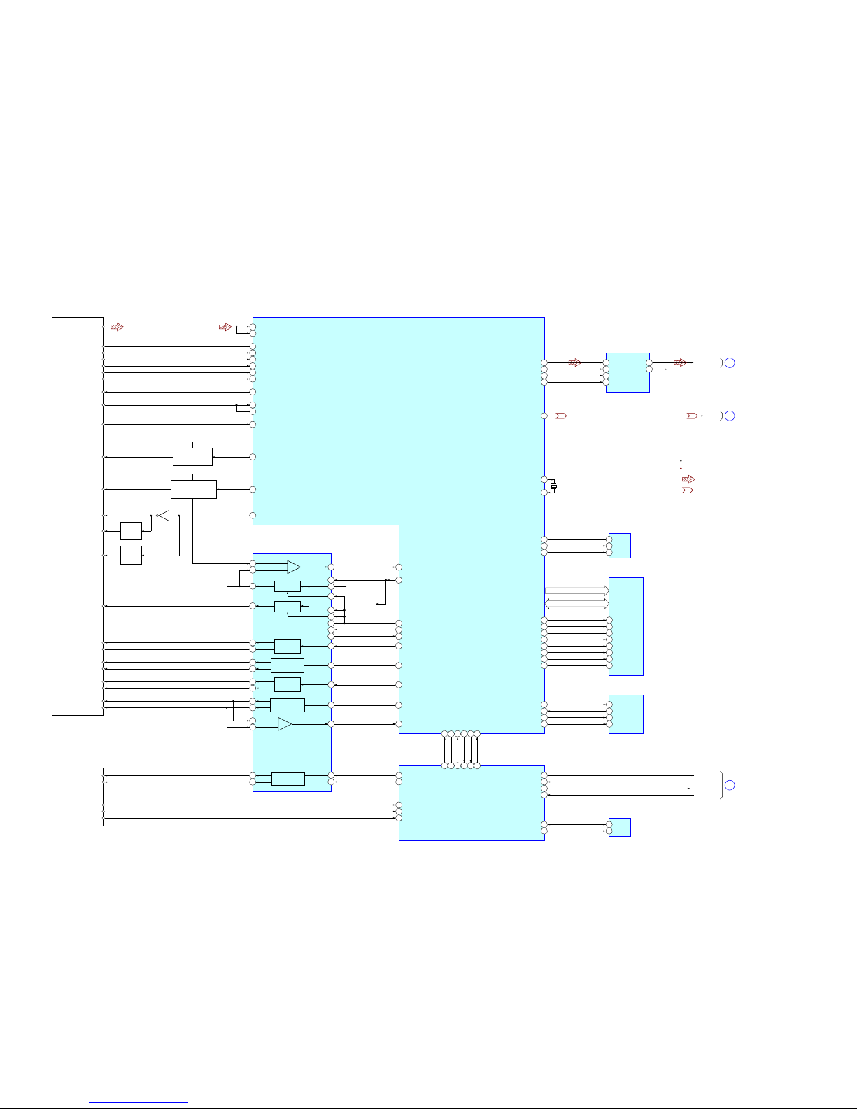
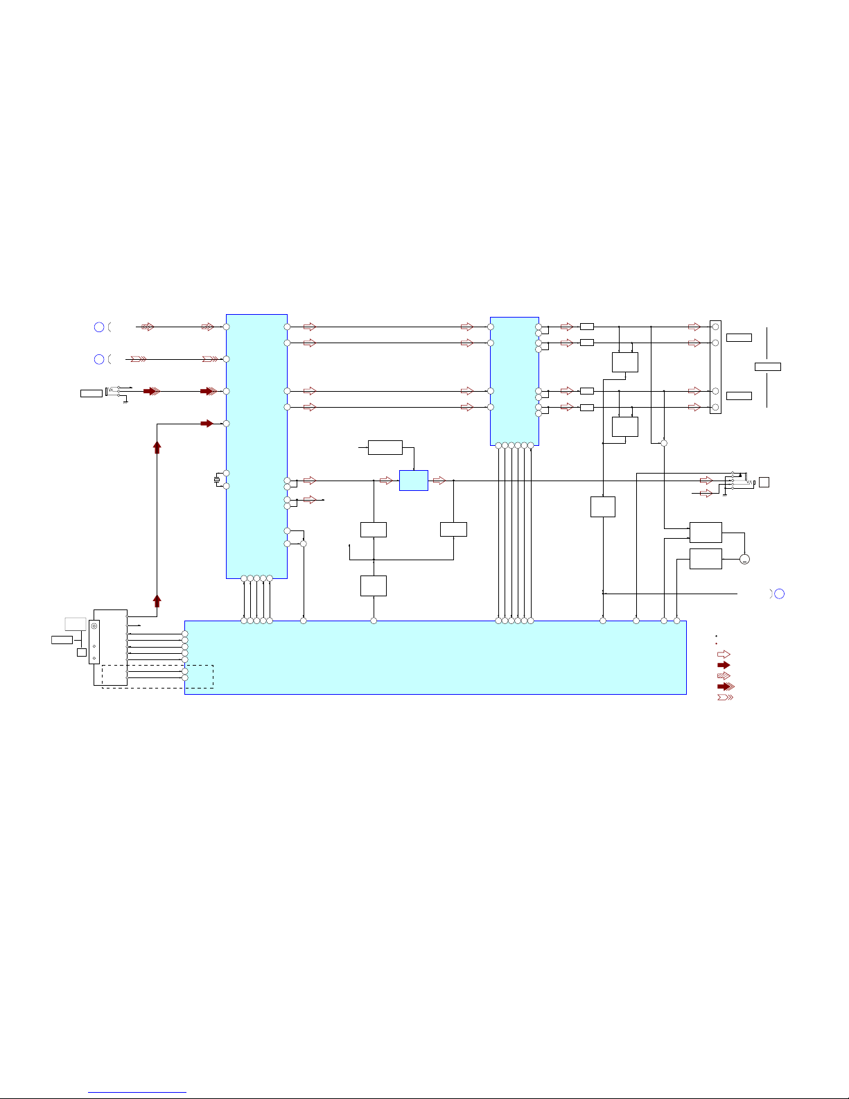
4-1. BLOCK DIAGRAM - SERVO Section -
RF
OPTICAL PICK-UP
BLOCK
(KHM-313CAB)
MS-214 BOARD
AUTO POWER
CONTROL (FOR CD)
Q003 (1/2)
RFIP
RFIN
RF_C
VOA/A
VOB/B
VOC/C
VOD/D
VOF/F+H
VOE/E+G
VC
LIMIT
PD
LD (780)
3
RF_B
2
RF_A
1
RF_D
4
RF_F
6
RF_E
5
V2O
LIMITSW
12
LDO1
17
MDI1
15
MDI2
16
AUTO POWER
CONTROL (FOR DVD)
Q003 (2/2)
FOCUS/TRACKING COIL DRIVE,
SPINDLE/SLED/LOADING MOTOR DRIVE
IC201
VREF
MUTE123
MUTE4
TSD_M
PS
RF AMP, SERVO DSP,
DVD/CD DECODER
IC005
SYSTEM CONTROLLER
IC100 (1/3)
VR (650)
VR (780)
MSW
Q002
VCC
LD (650)
LDO2
MSW
18
VM9V
OCSW1
43
FMO
FOO
DMO
TRO
VREFO
FWD
45
REV
44
IOPMON
SPFG
MUTE123
MUTE4
TSD_M
42
25
21
22
20
19
45
6
7
17
40
16
13
10
4
1
43
39
24
41
23
REG01
REG02
REG02
REG02
FCS+
FCS-
TRK+
TRK–
SP–
SP+
SL–
SL+
46
47
REGULATOR
32
31
30
REGULATOR
29
SPINDLE MOTOR
DRIVE
27
28
SLED MOTOR
DRIVE
FOCUS COIL
DRIVE
36
37
TRACKING COIL
DRIVE
35
34
DVD ON
SWITCH
Q001 (2/2)
DVD_SCO
23
DVD_SID
22
DVD_SOD
24
XIFCS
27
XSYSRST
21
DVD_XIFBUSY
25
IFSCK
IFCS#
IFSDO
IFBSY
IFSDI
PRST#
35 40 43418887
25
94
20
21
24
13
22
116
EEPROM
IC002
WP
EEWP
SCL
SDA
SCL
SDA
SD-RAM
IC008
FLASH ROM
IC003
UDQM
LDQM
CAS
RAS
WE
CLK
BA1
BA0
DQM1
DQM0
CAS#
RAS#
RWE#
RCLK
BA1
RD0 - RD15
RA0 - RA11
BA0
SF_CK
SF_DI
SF_DO
SF_CS#
SI
SO
_CS
SCK
6
5
2
136
37
38
39
RD0 - 15
DQ0 - DQ15
A0 - A11
RA0 - 11
AML RXD IN
AML TXD OUT
AML BUSY
AML RESET
37
38
35
36
78
80
66
75
77
76
55
65
ASDATA0
ALRCK
ACLK
ABCK
39
15
17
18
16
38
21
20
7
6
5
CD ON
SWITCH
Q001 (1/2)
126
125
118
127
115
119
120
114
CVBS
CVBS
AML RXD IN
AML TXD OUT
AML BUSY
AML RESET
128
CKSW1
42
TRG-SW
6
LDM+
LDM–
TRG-SW
CKSW1
OCSW1
26
33
34
EEPROM
IC150
EEPROM-CLK
EEPROM-DATA
SCL
SDA
6
5
50
49
99
R-CH
5AOUT-R
AUDIO
D/A CONVERTER
IC301
8AOUT-L
1SDATA
4MCLK
2SCLK
3 LRCK
A
DVD_L_OUT
B
C
VREFO1.4V
X001
27MHz
XTALO
XTALI
10
9
: DISC PLAY
SIGNAL PATH
R-ch is omitted due to same as L-ch.
: VIDEO
LOADING
MOTOR DRIVE
(Page 22)
(Page 23)
(Page 24)
HCD-SLK1i/SLK2i
HCD-SLK1i/SLK2i
2222
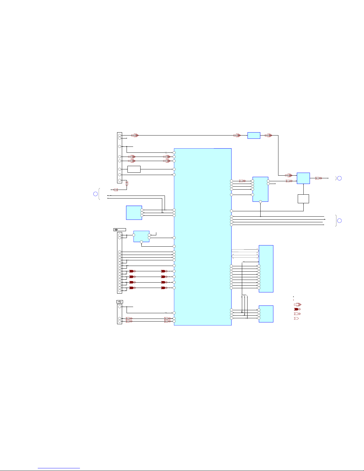
4-2. BLOCK DIAGRAM - AUDIO INPUT Section -
AUDIO DSP
IC401 (1/2)
CN1003
(iPod Dock)
27
28
R-CH
R-CH
4
6
30
LINE-OUT-L
LINE-OUT-R
23
iPod_VIDEO
I2CSDA
I2CSCK
Composite Video
8
iPod+5V
VBUS
USB D+
USB D–
iPod Detect
13
Acc PWR
32 iPod DET
iPod CP RESET
I2C SDA
I2C SCK
33 iPod Acc Power
14 USBB D–
13 USBB D+
11 USBB VBUS
WAKE UP
Q402
12I2C SCL
13I2C SDA
EEPROM
IC405
4RESET
CN401
3
2
1
VBUS5V
VBUS
D+
D–
5 USBA D–
4 USBA D+
2 USBA VBUS
CN402
4
11
8
VCC
SD/MMC-4 (VCC)
PRO/SD
INS
SD/MS INS
CARD VCC ENABLE
34 Card Vcc OverCurrent DET
1
10
SD-9 (DAT2)
DATA2
205
206
182
3
EN
DC_3.3V
4/OC
B+ SWITCH
IC406
1Vin
5VOUT
215
SD/MS DAT2
184
3
7
SD/MMC-1 (DAT3)
DATA3
SD/MS DAT3
183
15
6
BS
SD/MMC-2 (CMD)
SD CMD/MS BS
180
5
14
SCLK
SD/MMC-5 (CLK)
SD/MS CLK
181
12
18
SDIO/DATA0
SD/MMC-7 (DAT0)
SD/MS DAT0
187
13
19
DATA1
SD-8 (DAT1)
SD/MS DAT1
186
175
17
SD/MMC#CD
SD CARD DET
177
20
SD#WP
SD WP
176
BCK
MCLK
MDATA
212
LRCK
213
DAC SMUTE
178
IPOD USB SEL
211
214
UART Rx
AML BUSY
RESET
203
UART Tx
204
197
216
5
92
RSTN
10OUTR
AUDIO
D/A CONVERTER
IC606
11OUTL
3SDTI
1MCLK
2 BICK
4 LRCK
6SMUTE
iPod LINE AMP
IC612
iPod/USB
SELECT
SWITCH
IC613
SWITCH
CONTROL
Q610, 613
E
AML-L
SD-RAM
IC404
FLASH ROM
IC403
UDQM
LDQM
CAS
RAS
WE
CLK
BA1
BA0
M1 DQM1
M1 DQM0
M1 CAS n
M1 RAS n
M1 WE n
M1 CLKO
M1 BA1
M1 BA0
SPI C/M1 D0
SPI D/M1 D1
SPI Q/M1 D2
M1_DQ0
M1_DQ1
M1_DQ2
SPI CS
SI (D)
SQ (Q)
CS (S)
SCLK (C)
6
5
2
136
40
39
38
M1_DQ3 - 7, M1_D8 - 15
M1_DQ0 - M1_DQ2
M1_A0 - 12
76
77
60
71
73
72
48
58
39
15
17
18
CSM1 SCS0 n
75 19
16
38
21
20
D
AML RXD IN
AML TXD OUT
AML BUSY
AML RESET
C
: iPod
SIGNAL PATH
R-ch is omitted due to same as L-ch.
: MEMORY CARD
: USB
: VIDEO
M1 A0 - M1 A12
SPI WP/M1 D3, M1 D4 - M1 D15
DQ3 - DQ15
DQ0 - DQ2
A0 - A12
(Page
21)
(Page 23)
(Page 24)
HCD-SLK1i/SLK2i
HCD-SLK1i/SLK2i
2323
4-3. BLOCK DIAGRAM - AUDIO OUTPUT Section -
R-CH
J703
AUDUO IN
E
AML-L
A
DVD_L_OUT
TU1
TUNER (FM)
TUNER-L
PLL_DO
PLL_CE
TUNED
PLL_DI
PLL_CLK
TUNER-R R-CH
SYSTEM CONTROLLER
IC100 (2/3)
ST-CE
69
ST-CLK
RDS_INT
RDS_DATA
RDS-INT
18
RDS DATA
7
ST-DIN
72
71
ST-DOUT
70
ST-TUNED
68
(AEP)
FM 75:
COAXIAL
AM
ANTENNA
A/D CONVERTER,
DIGITAL AUDIO PROCESSOR
IC300
60 LINEIN7L
63 LINEIN8L
66 LINEIN9L
69 LINEIN10L
RIPPLE FILTER
Q401
MUTING
Q403
MUTING
Q412
PWM1_LD 92
PWM1_RD 96
PWM1_LI
93
LINEOUT1L
76
LINEOUT1R
77
PWM1_RI
97
J241
R-CH
R-CH
HEADPHONE
AMP
IC401
MUTING
CONTROL
Q404
R-CH
A+9V
HP DET
2
FAN-CONTROL
61
PROTECT FAN
63
HP MUTE
1
PROTECT AMP
54
PWM3_LI 5
PWM3_LD 4
PWM3_RI 9
PWM3_RD 8
i
OVER LOAD
DETECT
Q608, 609
OVER LOAD
DETECT
Q606, 607
L.P.F.
L.P.F.
L.P.F.
L.P.F.
SPEAKERS
FRONT R
TB601
+
+
FRONT L
DIGITAL POWER AMP
IC500
4 INPUT_A OUT_A
5 INPUT_B OUT_B
11 INPUT_D
10
52
44
INPUT_C
OUT_D
28
36OUT_C
OUT_A
OUT_B
53
45
OUT_D
29
37OUT_C
DSP-MUTE
80
DSP-VALID
79
DSP-CLK
78
DSP-DATA
77
DSP-RESET
81
/MUTE
I2C_SDA1
VALID
I2C_SCL1
/RESET
VACS
92
34 38 3910
33
/CLIP
56
/OTW253/OTW1
52
/SD
73
READY
55
/CLIP
/SD
/OTW2
/OTW1
READY
16 18 1917
15
/D-AMP-RESET
51
/RESET
2
+
+
M601
(FAN)
FAN MOT OR
DRIVE
Q600 - 602, 613
FAN PROTECT
DETECT
Q610 - 612
MM
PROTECT
DETECT
Q620
F
PROTECT_AMP
X385
24.576MHz
XTAL_OUT
XTAL_IN
86
87
: AUDIO
: DISC PLAY
SIGNAL PATH
R-ch is omitted due to same as L-ch.
: TUNER
: AUDIO IN
: USB
(Page 21)
(Page 22)
(Page 25)

HCD-SLK1i/SLK2i
HCD-SLK1i/SLK2i
2424
4-4. BLOCK DIAGRAM - VIDEO Section -
J702
VIDEO IN
B
CVBS
VIDEO SELECTOR
IC602
VIDEO A/D CONVERTER
IC605
DISPLAY CONTROLLER
IC401 (2/2)
12 D3 (DVD)
1AIP1A
13 D0 (iPod)
14 D1 (input)
22 SDA
21 SCL
VIDEO AMP
IC604
VIDEO AMP
IC1001
VIDEO AMP
IC603
COM 3
LCD SCL(SPI)
LCD B0 -
LCD B7
LCD G0 - LCD G7
LCD R0 - LCD R7
YOUT0 - 7
11 – 18
21 – 23, 25 – 27, 29, 30
136 – 139, 141 – 144145 – 149, 151 – 153155 – 162
SEL A
11
SEL B
10
J701
DVD VIDEO OUT
8 8
8 8
8 8
8 8
iPod_VIDEO
I2CSDA
I2CSCK
D
LCD901
LIQUID CRYSTAL
DISPLAY MODULE
DR0 - 7
DB0 - 7
DG0 - 7
SCL
165
193
LCD DCLK
DCLK
166
LCD HSYNC
HSYNC
167
LCD DE
DE
168
LCD VSYNC
VSYNC
169
LCD CS(SPI)
CS
170
LCD SDA(SPI)
SDA
171
LCD GBR
GBR
VDPA
VDNA
VGL
VGH
LED OUT
LED_I_SENCE
173
VGH10VCTL
VGHL CS0
118
VGHL CS1
119
LCD PWM
LED PWM
LED CS1
110
LED CS0
109
DC/DC
CONVERTER
Q604,
D601, 605 - 607, 615
B+ SWITCH
Q606, 607
DC/DC
CONVERTER
Q603,
D608, 609, 616, 617
+5.5V
REGULATOR
Q605, D612
DC/DC
CONVERTER
Q602, D618
–5.5V
REGULATOR
D613
VCOM
14
V1 - 14
NDAVO
PDAVO
BIAS
CIRCUIT
D+5V
HP–5V
91
85
87
RESETB 8 Video Dec RESET
656D0 - 656D7
194
AVID 26 Video Dec AVID
195
INTREQ/GPCL 27 Video Dec INTREQ/GPCL
196
PDN 28 Video Dec PDN
199
SCLK 9 Video Dec PCLK
200
VSYNC 24 Video Dec VSYNC
201
HSYNC 25 Video Dec HSYNC
202
FID/GLCO 23 Video Dec FID/GLCO
188
SELB
190
SELA
192
Video AMP B MUTE
191
209
210
Video AMP A MUTE
X601
14.31818MHz
XTAL2
XTAL1/OSC
6
5
X401
24MHz
OSCOUT
OSCIN
SIGNAL PATH
R-ch is omitted due to same as L-ch.
: VIDEO
(Page 21)
(Page 22)

HCD-SLK1i/SLK2i
HCD-SLK1i/SLK2i
2525
4-5. BLOCK DIAGRAM - PANEL, POWER SUPPLY Section -
D908
(AC IN)
D909
SWR1
SWITCHING REGULATOR
PVDD
AC-DET
P. CONT
PROTECT
+12V
REGULATOR
IC901
+5V
REGULATOR
IC900
+5V
REGULATOR
IC902
SOFT START
Q903, 904
REGULATOR
CONTROL
Q918, 919
OVER VOLTAGE
DETECT
Q910 - 912
D910 D912
D913
OVER CURRENT
DETECT
IC611
+3.3V
REGULATOR
IC906
+9V
REGULATOR
IC903
+3.3V
REGULATOR
IC907
+5V
REGULATOR
IC905
+9V
REGULATOR
IC904
A+3.3V
+1.8V
REGULATOR
IC610
DC_1.8V
+3.3V
REGULATOR
IC609
DC_3.3V
+1.2V
REGULATOR
IC601
DC_1.2V
+1.8V
REGULATOR
IC004
DVD+1.8V
+3.3V
REGULATOR
IC007
DVD A+3.3V
+3.3V
REGULATOR
IC001
RF+3.3V
A+5V
A+9V
LED+9V
D+12V
D+3.3V
D+5V
B+ SWITCH
Q914 - 917,
920 - 923
IC301_+5V
VM9V
DVD D+3.3V
DVD+5V
iPod+5V
VBUS5V
EVER+3.3V
AD-LINE_PULL-UP
D200
B+ SWITCH
Q905 - 907
+4V
REGULATOR
IC908
SYSTEM CONTROLLER
IC100 (3/3)
SIRCS IN
REMOTE
CONTROL
RECEIVER
IC242
PHOTO
DIODE
PH901
4
TP INT
75
TP RESET
76
TP SCL
48
TP SDA
47
POWER-KEY
74
LUX-SENSOR
94
AD-KEY-0 - 2
X110
32.768kHz
XCout
XCIN
11
10
X114
5MHz
XOUT
XIN
13
15
SONYLOGO LED28
D901, 902
(SONY LOGO)
LED DRIVE
Q901
BUZZER CONT3
BUZZER LEVEL
CONTROL
Q103
TP BUZZER26
BUZZER DRIVE
Q104
S261 - 269
KEY0
83 – 85
3
12RESET
60P. CONT
19PROTECT-INT
66USB POWER
57USB OC
58IPOD OC
67MTK POWER
RESET
SWITCH
Q202
RESET
SIGNAL
GENERATOR
Q201
PLAY LED
89
LED DRIVE
Q262
D267
PAUSE LED
90
LED DRIVE
Q263
D264
TIMER LED
87
LED DRIVE
Q264
D265
A. STBY LED
88
LED DRIVE
Q265
D266
LED DRIVE
Q261
D262
59
STBY-LED
D270
D261
TIMER
PAUSE
PLAY
ON/STANDBY
AUTO
STANDBY
F
PROTECT_AMP
TOUCH SENSOR
BOARD
BZ701
TP SDA
TP RESET
TP INT
TP SCL
B+ SWITCH
Q198, 199
AD-SWTICH
100
82DVD 3.3V MONITOR
20/AC-CUT
PVDD
AMBIENT
LIGHT
SENSOR
(Page 23)
HCD-SLK1i/SLK2i
HCD-SLK1i/SLK2i
2626
For Schematic Diagrams.
Note:
• All capacitors are in μF unless otherwise noted. (p: pF) 50
WV or less are not indicated except for electrolytics and
tantalums.
• All resistors are in Ω and 1/4 W or less unless otherwise
specifi ed.
• f : internal component.
• C : panel designation.
THIS NOTE IS COMMON FOR PRINTED WIRING BOARDS AND SCHEMATIC DIAGRAMS.
(In addition to this, the necessary note is printed in each block.)
• A : B+ Line.
• B : B– Line.
• Voltages and waveforms are dc with respect to ground
under no-signal conditions.
no mark : TUNER
• Voltages are taken with VOM (Input impedance 10 MΩ).
Voltage variations may be noted due to normal production
tolerances.
• Waveforms are taken with a oscilloscope.
Voltage variations may be noted due to normal production
tolerances.
• Circled numbers refer to waveforms.
• Signal path.
F : AUDIO
E : VIDEO
J : DISC PLAY
f : TUNER
p : USB
g : iPod
l : MEMORY CARD
i : AUDIO IN
• Abbreviation
AR : Argentina model
BR : Brazilian model
CH : Chinese model
CND : Canadian model
E2 : 120 V AC area in E model
E3 : 240 V AC area in E model
E51 : Chilean and Peruvian models
EA : Saudi Arabia model
KR : Korean model
MX : Mexican model
SP : Singapore model
TH : Thai model
• The voltage and waveform of CSP (chip size package)
cannot be measured, becaise its lead layout is different
from that of conventional IC.
For Printed Wiring Boards.
Note:
• X : Parts extracted from the component side.
• Y : Parts extracted from the conductor side.
• x : Parts mounted on the conductor side.
• f : Internal component.
• : Pattern from the side which enables seeing.
(The other layers' patterns are not indicated.)
• Indication of transistor.
C
B
These are omitted.
E
Q
B
These are omitted.
CE
Q
• Abbreviation
AR : Argentina model
BR : Brazilian model
CH : Chinese model
CND : Canadian model
E2 : 120 V AC area in E model
E3 : 240 V AC area in E model
E51 : Chilean and Peruvian models
EA : Saudi Arabia model
KR : Korean model
MX : Mexican model
SP : Singapore model
TH : Thai model
• Lead layouts
surface
CSP (Chip Size Package) Lead layout of conventional IC
Caution:
Pattern face side:
(Conductor Side)
Parts face side:
(Component Side)
Parts on the pattern face side seen
from the pattern face are indicated.
Parts on the parts face side seen from
the parts face are indicated.
• DISPLAY board is multi-layer printed board. However, the
patterns of intermediate-layers have not been included in
this diagrams.
• Circuit Boards Location
Caution:
Pattern face side:
(SIDE B)
Parts face side:
(SIDE A)
Parts on the pattern face side seen
from the pattern face are indicated.
Parts on the parts face side seen from
the parts face are indicated.
Note: The components identifi ed by mark 0 or
dotted line with mark 0 are critical for safety.
Replace only with part number specifi ed.
Note: Les composants identifi és par une marque
0 sont critiques pour la sécurité.
Ne les remplacer que par une piéce portant
le numéro spécifi é.
MS-214 board
LCD board
TOUCH PANEL board
JACK board
TERMINAL board
SWITCHING REGULATOR
KEY-RIGHT board
MAIN board
KEY-LEFT board
HP board
DISPLAY board
IP board
TUNER (FM/AM)

HCD-SLK1i/SLK2i
HCD-SLK1i/SLK2i
2727
4-6. SCHEMATIC DIAGRAM - DISPLAY Section (1/7) -
• See page 50 for Waveforms. • See page 50 for IC Block Diagrams. • See page 55 for IC Pin Function Description.
DISPLAY
(2/7)
2
BOARD
(2/7)
3
DISPLAY
BOARD
1
BOARD
DISPLAY
(2/7)
8
(3/7)
DISPLAY
BOARD
BOARD
5
(4/7)
DISPLAY
BOARD
DISPLAY
7
(4/7)
IC B/D
1
1.2
3.3
3.3
1.6
2.6
3.3
3.3
3.3
3.3
3.3
3.3
0
3.3
3.3
3.3
3.3
3.3
3.3
1.2
3.3
3.3
3.3
3.3
0
0
3.3
3.3
0.6
3.3
0
3.3
1.6
0
0
3.1
2.5
3.3
3.3
3.3
3.3
1.6
1.6
0
3.3
0
0
3.3
3.3
0
5
3.3
000
3.3
0
5
3.3
000
3.3
3.3
0.3
0.3
0.3
3.3
0.3
0.3
0.3
1.2
0.3
0.3
3.3
3.3
3.3
3.3
1.5
1.5
1.5
1.7
3.3
1.7
1.6
1.6
1.601.6
1.6
1.6
1.7
1.7
3.3
1.7
1.7
1.7
0
1.7
0
0
0
0
0.6
2.8
2.8
2.8
3.3
3.3
3.3
3.3
1.2
0.5
0
2.7
2.7
2.8
0.5
3.3
1.4
0
3.3
3.3
3.3
0.6
0.2
0.2
0.3
0.6
0.6
0.6
0.8
0.8
0.2
0.2
0.3
3.3
0.6
0.6
0.6
0.8
0.8
0.2
0.2
0.3
0.6
0.6
0.6
0.8
0.8
3.3
1.2
3.300
0.5
0.500
0.5
0.4
3.3
3.3
3.3
3.3
0
R403
1k
R404
22
R40722R408
22
R40922R410
0.1
R411
0.1
R412
0.1
R413
0.1
R414
0
R415
1k
R416
FB403
0.1
C417
0.1
C418
0.1
C419
0.1
C420
0.1
C421
0.1
C422
0.1
C423
0.1
C424
0.1
C425
0.1
C426
0.1
C427
0.1
C428
0.1
C429
0.1
C430
0.1
C431
0.1
C432
0.1
C434
0.1
C435
0.1
C436
LCDPWB
LEDPWM
LEDCS0
LEDCS1
VGHLCS0
100R440
100R441
100R445
100R446
10k
R451
180
R452
180
R453
180R454
180R455
180R456
180R457
0
R460
10k
R461
100
R463
4.7k
R464
100
R465
100
R468
0.1
C443
FB410
FB411
10kR478
10kR479
100
R481
100R482
100R483
100R484
100
R485
100
R486
100
R487
100
R488
100
R489
100
R490
100
R491
100
R492
100
R493
100
R494
100
R495
100
R496
0.1
C449
0.1
C450
0.1
C451
0.1
C452
R498
4.7k
4.7k
R500
4.7k
R510
4.7k
R513
4.7k
R515
4.7k
R517
R519
4.7k
R521
4.7k
4.7k
R523
R525
4.7k
100R526
100
R527
100
R528
100
R529
100
R530
100
R532
10V
100
C453
10V
100
C455
10V
100
C456
10V
100
C458
SELA
SELB
VideoAMP_A_MUTE
VideoAMP_B_MUTE
VideoDecRESET
VideoDecPDN
VideoDecPCLK
VideoDecAVID
VideoDecINTREQ/GPCL
VideoDecVSYNC
VideoDecHSYNC
VideoDecFID/GLCO
656D0
656D1
656D2
656D3
656D4
656D5
656D6
656D7
DACS-MUTE
JTAGTMS/I2SMCLK
JTAGTDI/I2SBCK
JTAGTCK/I2SLRCK
JTAGTDO/I2SMDATA
VGH10VCTL
100
R536
10
R542
10
R545
10
R547
0.047
C465
0.047
C466
0.047
C469
0.047
C470
10
R548
JL471
JL472
JL473
JL474
JL475
JL476
JL477
JL478
JL479
JL487
JL489
JL490
JL491
JL493
JL494
JL495
JL496
JL497
JL498
JL530
JL531
JL532
JL534
1234
L401
10k
R447
1 23 45 67 89101112131415161718192021222324252627282930313233343536373839404142434445464748495051525354
57
58
59
60
61
62
63
64
65
66
67
68
69
70
71
72
73
74
75
76
77
78
79
80
81
82
83
84
85
86
87
88
89
90
91
92
93
94
95
96
97
98
99
100
101
102
103
104
105
106
107
108
113114115116117118119120121122123124125126127128129130131132133134135136137138139140141142143144145146147148149150151152153154155156157158159160161162
169
170
171
172
173
174
175
176
177
178
179
180
181
182
183
184
185
186
187
188
189
190
191
192
193
194
195
196
197
198
199
200
201
202
203
204
205
206
207
208
209
210
211
212
213
214
215
216
56
55
110109112111
165
164
163
167
168
166
AML6226D
IC401
USBA ID
USBA VBUS
USB VDD3.3
USBA D+
USBA D-
USBA VSS3.3
USBA txrtune
USBA VSS3.3
USBA VDD3.3
USBB ID
USBB VBUS
USBB VDD3.3
USBB D+
USBB D-
USBB VSS
USBB txrtune
USBB VSS3.3C
USBB VDD3.3
PLL VDD3.3
PLL VSS
656D0
656D1
656D2
VDD3.3
656D3
656D4/MDATA
656D5
VDD1.2
656D6
656D7
DVSS
iPod DET
iPod Acc Power
Card Vcc OverCurrent DET
SPI CSNCSPI HOLD
SPI C/M1 D0
SPI D/M1 D1
SPI Q/M1 D2
SPI WP/M1 D3
VDD3.3
M1 D4
M1 D5
DVSS
M1 D6
M1 D7
M1 DQM0
M1 D15
M1 D14
M1 D13
M1 D12
M1 D11
VDD3.3
M1 D8
M1 DQM1
DVSS
M1 CLK0
M1 CKE
M1 A12
M1 A11
M1 A9
M1 A8
M1 A7
M1 A6
M1 A5
M1 A4
VDD3.3
M1 WE n
M1 CAS n
M1 RAS n
VDD1.2
M1 SCS0 n
M1 BA0
M1 BA1
DVSS
M1 A10
M1 A0
M1 A1
M1 A2
M1 A3
LCD PWM180
LCD PWM
VDD3.3
LED PWM
LED PWM180
Remote Input
LED BackLightIC Cont
VGH10VCTL
IPOD USB SEL
TADC AV3.3
TADC CH11
TADC CH10
TADC CH9
TADC CH8
TADC CH7
TADC CH6
TADC CH5
TADC CH4
TADC CH3
TADC CH2
TADC CH1
TADC CH0
TADC CAP+
TADC CAP-
TADC AGND
RTC XOUT
RTC XIN
RTC PDAC GND
REF12 VX
VREF12 FB
VGHL CS0
VGHL CS1
AOUT SPRC
AOUT SPR
AOUT HPR
AOUT HPRC
AOUT AVSS3.3
AOUT REFN
AOUT VCM
AOUT REFP
AOUT AVDD3.3
AOUT HPLC
AOUT HPL
AOUT SPL
AOUT SPLC
NC
VDD1.2
VDD3.3
LCD R0
LCD R1
LCD R2
LCD R3
DVSS
LCD R4
LCD R5
LCD R6
LCD R7
LCD G0
LCD G1
LCD G2
LCD G3
LCD G4
VDD3.3
LCD G5
LCD G6
LCD G7
DVSS
LCD B0
LCD B1
LCD B2
LCD B3
LCD B4
LCD B5
LCD B6
LCD B7
LCD VSYNC
LCD CS(SPI)
LCD SDA(SPI)
DVSS
LCD GBR
iPod LINE MUTE
SD/MS INS
SD WP
SD CARD DET
DAC SMUTE
VDD3.3
SD CMD/MS BS
SD/MS CLK
iPod CP RESET
SD/MS DAT3
SD/MS DAT2
VDD1.2
SD/MS DAT1
SD/MS DAT0
SELB
DVSS
SELA
Video AMP A MUTE
Video AMP B MUTE
Video Dec RESET
Video Dec AVID
Video Dec INTREQ/GPCL
Video Dec PDN
AML BUSY
VDD3.3
Video Dec PCLK
Video Dec VSYNC
Video Dec HSYNC
Video Dec FID/GLCO
UART Rx
UART Tx
I2C SDA
I2C SCK
VDD3.3
VSS3.3
OSCIN
OSCOUT
MCLK
BCK
LRCK
MDATA
CARD VCC ENABLE
RESET
M1 D10
M1 D9
LED CS0
LED CS1
RTC GPO
RTC VBAT
VDD1.2
VDD3.3
LCD SCL(SPI)
LCD DCLK
LCD HSYNC
LCD DE
JL587
JL588
1
2
3
4
5
6
7
8
9
10
11
12
13
13P
CN403
GND
3VCC
NC
RESET
DI
TMS
NC(NC)
TDO
NC
TCK
NC
NC
NC
4.7k
R563
4.7k
R564
4.7k
R565
4.7k
R566
4.7k
R569
4.7k
R570
IPOD_USB_SEL
R577
4.7k
10k
R578
10k
R579
BD2220G-TR
IC406
1
Vin2GND3EN
4
/OC
5
VOUT
820
R472
1000p
C615
20P
CN402
1SD-9(DAT2)
2VSS
3SD/MMC-1(DAT3)
4VCC
5SCLK
6SD/MMC-2(CMD)
7DATA3
8INS
9SD/MMC-3(GND)
10DATA2
11SD/MMC-4(VCC)
12SDIO/DATA0
13DAT1
14SD/MMC-5(CLK)
15BS
16VSS
17SD/MMC#CD
18SD/MMC-7(DAT0)
19SD-8(DAT1)
20SD#WP
1000p
C642
0
R582
FB414
FB415
FB416
FB417
FB418
FB419
FB405
FB408
1.2k
R470
1.2k
R471
FB421
0
R539
0
R540
0
R541
4.7k
R476
M1_DQ7
M1_D15
M1_D14
M1_D13
M1_D12
M1_D11
M1_D10
M1_D9
M1_D8
M1_DQM1
M1_CLK0
M1_CS
M1_A0
M1_A1
M1_A2
M1_A3
CS
DE
JTAGTMS/I2SMCLK
JTAGTDI/I2SBCK
JTAGTDO/I2SMDATA
M1_DQ4
M1_DQ5
GRB
DACS-MUTE
DACS-MUTE
JL785
B[7]
B[6]
B[5]
B[4]
B[3]
B[2]
B[1]
B[0]
G[7]
G[6]
G[5]
G[4]
G[3]
G[2]
G[1]
G[0]
R[7]
R[6]
R[5]
R[4]
R[3]
R[2]
R[1]
R[0]
M1_A4
M1_A11
M1_A9
M1_A7
M1_A6
M1_A5
M1_A8
M1_A10
M1_BA1
M1_BA0
M1_RAS
M1_CAS
M1_WE
M1_A12
M1_DQM0
SDA
SCL
DCLK
M1_DQ6
JTAGTCK/I2SLRCK
JTAGTDO/I2SMDATA
JTAGTMS/I2SMCLK
JTAGTDI/I2SBCK
M1_DQ3
M1_DQ2
M1_DQ0
M1_DQ1
JTAGTCK/I2SLRCK
IC406
B+ SWITCH
IC401
DISPLAY CONTROLLER, AUDIO DSP
DISPLAY BOARD
(1/7)
2
1
12
14
13
3
8
10
7
4
9
5
11
6
15
23172219252120
16
18
24
PRO/SD
J
4
B
166911
D
N
O
P
15
H
L
10
K
1735 12
C
F
18
M
1 19
E
8
G
2014
A
2 13
I
7
(Page 28)
(Page
30)
(Page 28)
(Page 30)
(Page 29)
(Page 28)
 Loading...