

Page 1
HCD-SHAKE7
SERVICE MANUAL
Ver. 1.2 2013.11
• HCD-SHAKE7 is the tuner, USB, CD player, Bluetooth, NFC
and amplifi er section in SHAKE-7.
Model Name Using Similar Mechanism NEW
Amplifi er section
The following are measured at
Mexican model:
AC 120 V – 240 V, 60 Hz
Other models:
AC 120 V – 240 V, 50/60 Hz
Tweeters/woofers
Power Output (rated):
320 W + 320 W (at 4 ohms, 1 kHz,
1% THD)
RMS output power (reference):
520 W + 520 W (per channel at
4 ohms, 1 kHz)
Mid speakers
Power Output (rated):
240 W + 240 W (at 5 ohms, 1 kHz,
1% THD)
RMS output power (reference):
385 W + 385 W (per channel at
5 ohms, 1 kHz)
Subwoofers
Power Output (rated):
320 W + 320 W (at 4 ohms, 100 Hz,
1% THD)
RMS output power (reference):
520 W + 520 W (per channel at
4 ohms, 100 Hz)
Inputs
TV/DVD/SAT (AUDIO IN) L/R
Voltage 2 V, impedance 47 kilohms
PC/GAME (AUDIO IN) L/R
Voltage 2 V, impedance 47 kilohms
MIC
Sensitivity 1 mV, impedance 10 kilohms
A (USB), B (USB) port: Type A
USB section
Supported bit rate
WMA:
48 kbps – 192 kbps, VBR, CBR
AAC:
48 kbps – 320 kbps, VBR, CBR
Sampling frequencies
WMA: 44.1 kHz
AAC: 44.1 kHz
Supported USB device
Mass Storage Class
Maximum current
500 mA
CD Section
Disc/USB section
Supported bit rate
MPEG1 Layer-3:
32 kbps – 320 kbps, VBR
MPEG2 Layer-3:
8 kbps – 160 kbps, VBR
MPEG1 Layer-2:
32 kbps – 384 kbps, VBR
Sampling frequencies
MPEG1 Layer-3:
32 kHz/44.1 kHz/48 kHz
MPEG2 Layer-3:
16 kHz/22.05 kHz/24 kHz
MPEG1 Layer-2:
32 kHz/44.1 kHz/48 kHz
Disc player section
System
Compact disc and digital audio system
Laser Diode Properties
Emission Duration: Continuous
Laser Output*: Less than 44.6 µW
* This output is the value
measurement at a distance of
200 mm from the objective lens
surface on the Optical Pick-up
Block with 7 mm aperture.
Frequency response
20 Hz – 20 kHz
Signal-to-noise ratio
More than 90 dB
Dynamic range
More than 88 dB
Tuner section
FM stereo, FM/AM superheterodyne tuner
Antenna:
FM lead antenna
AM loop antenna
FM tuner section
Tuning range
87.5 MHz – 108.0 MHz
(50 kHz step)
AM tuner section
Tuning range
Pan American models:
531 kHz – 1,710 kHz (9 kHz step)
530 kHz – 1,710 kHz (10 kHz step)
CD Mechanism Type CDM90-DVBU202//M
Optical Pick-up Name CMS-S76RFS7G
SPECIFICATIONS
E Model
Saudi Arabian model:
531 kHz – 1,602 kHz (9 kHz step)
Other models:
531 kHz – 1,602 kHz (9 kHz step)
530 kHz – 1,610 kHz (10 kHz step)
Bluetooth section
Communication system
Bluetooth Standard version 3.0 +
EDR (Enhanced Date Rate)
Output
Bluetooth Standard Power Class 2
Maximum communication range
Line of sight approx. 10m
Frequency band
2.4 GHz band (2.4000 GHz – 2.4835 GHz)
Modulation method
FHSS (Freq Hopping Spread Spectrum)
Compatible Bluetooth profiles
A2DP (Advanced Audio Distribution
Profile)
AVRCP 1.3 (Audio Video Remote
Control Profile)
Supported codecs
SBC (Sub Band Codec)
AAC (Advanced Audio Coding)
1)
The actual range will vary depending on
factors such as obstacles between devices,
magnetic fields around a microwave oven,
static electricity, reception sensitivity,
antenna’s performance, operating system,
software application, etc.
2)
Bluetooth standard profiles indicate the
purpose of Bluetooth communication
between devices.
General
Power requirements
Mexican model:
AC 120 V – 240 V, 60 Hz
Other models:
AC 120 V – 240 V, 50/60 Hz
Power consumption
420 W
Dimensions (w/h/d) (excl. speakers)
(Approx.) (Except AR)
500 mm × 220 mm × 380 mm
1)
2)
Dimensions (w/h/d) (excl. speakers) (AR)
500 mm × 220 mm × 380 mm
Mass (excl. speakers) (Approx.) (Except AR)
8.4 kg
Mass (excl. speakers) (AR)
8.4 kg
Supplied accessories
Remote control (1)
R6 (Size AA) batteries (2)
FM lead/AM loop antenna (1)
Design and specifications are subject to
change without notice.
License and Trademark Notice
• “WALKMAN” and “WALKMAN” logo
are registered trademarks of Sony Corporation.
• MPEG Layer-3 audio coding technology
and patents licensed from Fraunhofer IIS
and Thomson.
• Windows Media is either a registered
trademark or trademark of Microsoft
Corporation in the United States and/or
other countries.
• This product is protected by certain
intellectual property rights of Microsoft
Corporation. Use or distribution of
such technology outside of this product
is prohibited without a license from
Microsoft or an authorized Microsoft
subsidiary.
• The Bluetooth® word mark and logos are
registered trademarks owned by Bluetooth
SIG, Inc. and any use of such marks by
Sony Corporation is under license. Other
trademarks and trade names are those of
their respective owners.
• The N Mark is a trademark or registered
trademark of NFC Forum, Inc. in the
United States and in other countries.
• Android is a trademark of Google Inc.
• All other trademarks and registered
trademarks are of their respective holders.
In this manual, ™ and ® marks are not
specified.
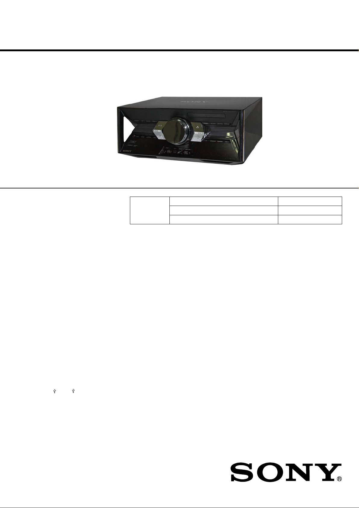
MINI HI-FI COMPONENT SYSTEM
9-890-619-03
2013K80-1
2013.11
©
Sony Corporation
Published by Sony EMCS (Malaysia) PG Tec
Page 2
HCD-SHAKE7
SAFETY CHECK-OUT
After correcting the original service problem, perform the following
safety check before releasing the set to the customer:
Check the antenna terminals, metal trim, “metallized” knobs,
screws, and all other exposed metal parts for AC leakage. Check
leakage as described below.
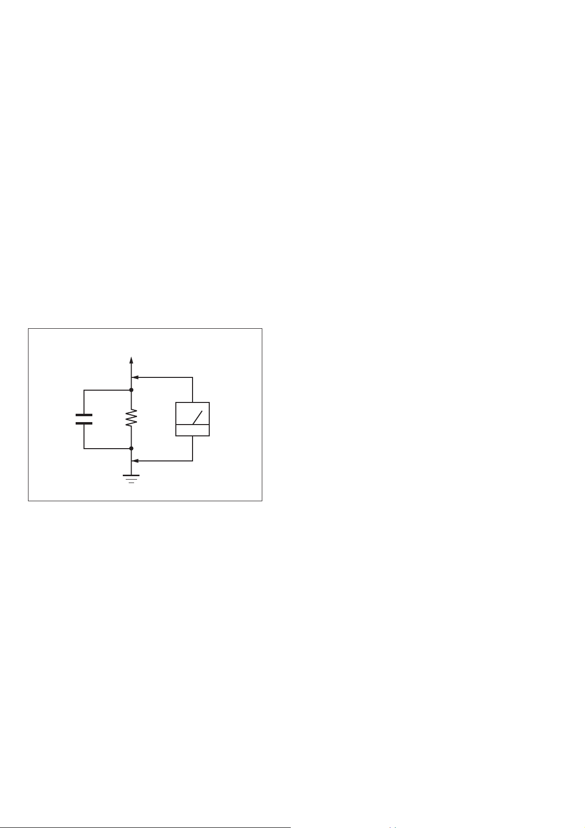
LEAKAGE TEST
The AC leakage from any exposed metal part to earth ground and
from all exposed metal parts to any exposed metal part having a
return to chassis, must not exceed 0.5 mA (500 microamperes).
Leakage current can be measured by any one of three methods.
1. A commercial leakage tester, such as the Simpson 229 or RCA
WT-540A. Follow the manufacturers’ instructions to use these
instruments.
2. A battery-operated AC milliammeter. The Data Precision 245
digital multimeter is suitable for this job.
3. Measuring the voltage drop across a resistor by means of a
VOM or battery-operated AC voltmeter. The “limit” indication
is 0.75 V, so analog meters must have an accurate low-voltage
scale. The Simpson 250 and Sanwa SH-63Trd are examples
of a passive VOM that is suitable. Nearly all battery operated
digital multimeters that have a 2V AC range are suitable. (See
Fig. A)
To Exposed Metal
Parts on Set
AC
1.5 kΩ0.15 μF
Earth Ground
voltmeter
(0.75 V)
Fig. A. Using an AC voltmeter to check AC leakage.
SAFETY-RELATED COMPONENT WARNING!
COMPONENTS IDENTIFIED BY MARK 0 OR DOTTED LINE
WITH MARK 0 ON THE SCHEMATIC DIAGRAMS AND IN
THE PARTS LIST ARE CRITICAL TO SAFE OPERATION.
REPLACE THESE COMPONENTS WITH SONY PARTS
WHOSE PART NUMBERS APPEAR AS SHOWN IN THIS
MANUAL OR IN SUPPLEMENTS PUBLISHED BY SONY.
2
Page 3

TABLE OF CONTENTS
HCD-SHAKE7
1. SERVICING NOTES ............................................. 4
2. DISASSEMBLY
2-1. Side-L Panel Assy, Side-R Panel Assy, Top Panel .......... 7
2-2. Back Panel Section ......................................................... 8
2-3. Loading Panel Assy ........................................................ 8
2-4. CDM90-DVBU202//M ................................................... 9
2-5. Front Panel Section ......................................................... 9
2-6. MOTHERBOARD Board ............................................... 10
2-7. SWITCHING REGULATOR (SMG-1800) .................... 11
2-8. Service Optical Device, Wire (Flat Type) ....................... 12
3. STORM TEST MODE .......................................... 13
4. ELECTRICAL CHECK ......................................... 16
5. TROUBLESHOOTING .......................................... 17
6. DIAGRAMS
6-1. Block Diagram - RS SERVO, USB Section - ................. 23
6-2. Block Diagram - MAIN Section - ................................... 24
6-3. Block Diagram - AMP Section - ..................................... 25
6-4. Block Diagram
- PANEL, POWER SUPPLY Section - ........................... 26
6-5. Printed Wiring Board
- MOTHERBOARD Board (Component Side) - ............ 28
6-6. Printed Wiring Board
- MOTHERBOARD Board (Conductor Side) - ............. 29
6-7. Schematic Diagram
- MOTHERBOARD Board (1/10) - ............................... 30
6-8. Schematic Diagram
- MOTHERBOARD Board (2/10) - ............................... 31
6-9. Schematic Diagram
- MOTHERBOARD Board (3/10) - ............................... 32
6-10. Schematic Diagram
- MOTHERBOARD Board (4/10) - ............................... 33
6-11. Schematic Diagram
- MOTHERBOARD Board (5/10) - ............................... 34
6-12. Schematic Diagram
- MOTHERBOARD Board (6/10) - ............................... 35
6-13. Schematic Diagram
- MOTHERBOARD Board (7/10) - ............................... 36
6-14. Schematic Diagram
- MOTHERBOARD Board (8/10) - ............................... 37
6-15. Schematic Diagram
- MOTHERBOARD Board (9/10) - ............................... 38
6-16. Schematic Diagram
- MOTHERBOARD Board (10/10) - ............................. 39
6-17. Printed Wiring Board - DISPLAY Board - ..................... 40
6-18. Schematic Diagram - DISPLAY Board - ........................ 41
6-19. Printed Wiring Board
- VOLUME Board (Component Side) - .......................... 42
6-20. Printed Wiring Board
- VOLUME Board (Conductor Side) - ........................... 43
6-21. Schematic Diagram - VOLUME Board - ....................... 44
6-22. Printed Wiring Board 6-23. Schematic Diagram 6-24. Printed Wiring Board 6-25. Schematic Diagram 6-26. Printed Wiring Board 6-27. Schematic Diagram 6-28. Printed Wiring Board 6-29. Schematic Diagram 6-30. Printed Wiring Boards 6-31. Schematic Diagram -
BUTTON_L Board - ................. 45
BUTTON_L Board - .................... 46
BUTTON_R Board - ................. 47
BUTTON_R Board - ................... 48
MIC Board - .............................. 48
MIC Board - ................................. 49
USB Board - .............................. 49
USB Board - ................................ 50
RGB BAR Boards - ................. 51
RGB BAR Boards - ..................... 52
7. EXPLODED VIEWS
7-1. Side Panel Section .......................................................... 67
7-2. Back Panel Section ......................................................... 68
7-3. Front Panel Section ......................................................... 69
7-4. Chassis Section ............................................................... 70
7-5. CD Mechanism Section (CDM90-DVBU202//M) ......... 71
8. ELECTRICAL PARTS LIST .............................. 72
3
Page 4
HCD-SHAKE7
Ver. 1.2
SECTION 1
SERVICING NOTES
Notes on chip component replacement
• Never reuse a disconnected chip component.
• Notice that the minus side of a tantalum capacitor may be
damaged by heat.
Flexible Circuit Board Repairing
• Keep the temperature of the soldering iron around 270 °C
during repairing.
• Do not touch the soldering iron on the same conductor of the
circuit board (within 3 times).
• Be careful not to apply force on the conductor when soldering
or unsoldering.
UNLEADED SOLDER
Boards requiring use of unleaded solder are printed with the
leadfree mark (LF) indicating the solder contains no lead.
(Caution: Some printed circuit boards may not come printed with
the lead free mark due to their particular size)
: LEAD FREE MARK
Unleaded solder has the following characteristics.
• Unleaded solder melts at a temperature about 40 °C higher
than ordinary solder.
Ordinary soldering irons can be used but the iron tip has to be
applied to the solder joint for a slightly longer time.
Soldering irons using a temperature regulator should be set to
about 350 °C.
Caution: The printed pattern (copper foil) may peel away if
the heated tip is applied for too long, so be careful!
• Strong viscosity
Unleaded solder is more viscous (sticky, less prone to fl ow)
than ordinary solder so use caution not to let solder bridges
occur such as on IC pins, etc.
• Usable with ordinary solder
It is best to use only unleaded solder but unleaded solder may
also be added to ordinary solder.
CAUTION
Use of controls or adjustments or performance of procedures
other than those specifi ed herein may result in hazardous radiation
exposure.
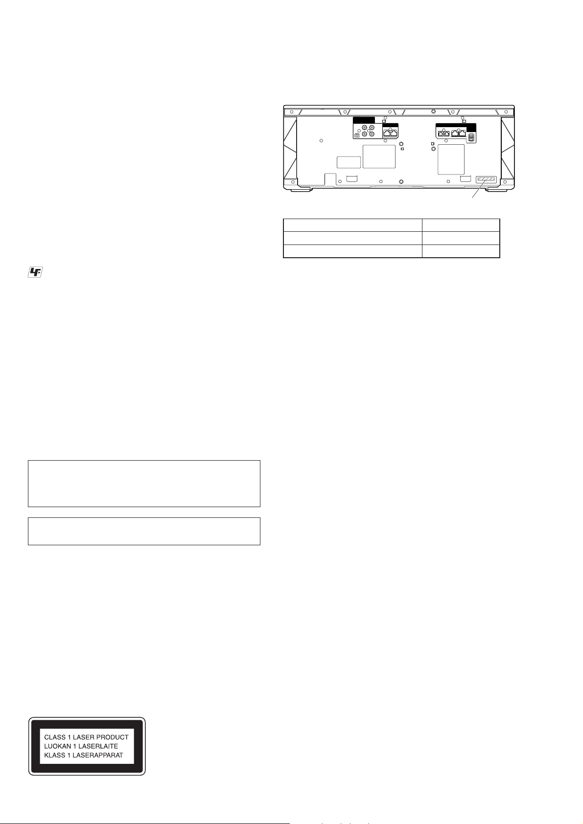
MODEL IDENTIFICATION
- BACK PANEL -
PART No.
Model Part No.
E2, E4, E51, EA, MY, SAF, AR
MX
• Abbreviation
AR : Argentina model
E2 : 120 V AC area in E model
E4 : African model
E51 : Chilean and Peruvian models
EA : Saudi Arabian model
MX : Mexican model
MY : Malaysia model
SAF : South African model
4-449-865-0[]
4-449-865-1[]
PLAYABLE DISCS
• AUDIO CD
• CD-R/CD-RW
– audio data
– MP3 fi les that conforms to ISO9660 Level 1/Level 2, or
Joliet (expansion format).
Notes
• MP3 (MPEG 1 Audio Layer-3) is a standard format defi ned
by ISO (International Organization for Standardization) which
compresses audio data. MP3 fi les must be in MPEG 1 Audio
Layer-3 format.
• The system can only play back MP3 fi les that have a fi le
extension of “.mp3”.
NOTES ON HANDLING THE OPTICAL PICK-UP BLOCK
OR BASE UNIT
The laser diode in the optical pick-up block may suffer electrostatic
break-down because of the potential difference generated by the
charged electrostatic load, etc. on clothing and the human body.
During repair, pay attention to electrostatic break-down and also
use the procedure in the printed matter which is included in the
repair parts.
The fl exible board is easily damaged and should be handled with
care.
NOTES ON LASER DIODE EMISSION CHECK
The laser beam on this model is concentrated so as to be focused
on the disc refl ective surface by the objective lens in the optical
pickup block. Therefore, when checking the laser diode emission,
observe from more than 30 cm away from the objective lens.
This appliance is
claassifi ed as a CLASS 1
LASER product. This
label is located on the
rear exterior.
NOTE OF REPLACING THE IC304, IC305, IC306 AND
IC902 ON THE MOTHERBOARD BOARD
IC304, IC305 IC306 and IC902 on the MOTHERBOARD
board cannot exchange with single. When these parts on the
MOTHERBOARD board are damaged, exchange the entire
mounted board.
NOTE OF REPLACEMENT OF THE MS-476 BOARD
When the MS-476 board is defective, exchange the entire
LOADING ASSY (T).
RELEASING THE DISC TRAY LOCK
The disc tray lock function for the antitheft of an demonstration
disc in the store is equipped.
Releasing Procedure:
1. Press [\/1] button to turn the power on.
2. Press the [CD] button to select CD function.
3. While pressing the [x] button, press the [OPTIONS] button
for more 5 seconds).
4. The message “UNLOCKED” is displayed and the disc tray is
unlocked.
Note: When “LOCKED” is displayed, the slot lock is not released by
turning power on/off with the [\/1] button.
4
Page 5
HCD-SHAKE7
Ver. 1.1
NOTE OF REPLACING MOTHERBOARD BOARD OR
BLUETOOTH MODULE OR RC-S801/A (WW) BOARD
When the MOTHERBOARD board or BLUETOOTH module or
RC-S801/A (WW) board are replaced, please execute the below
service mode.
Pairing this system with a
1. Press the [\/1] button to turn the power on.
2. Place the Bluetooth device within 1 meter from the system.
3. Press BLUETOOTH on the unit to select Bluetooth function.
“BLUETOOTH” appears in the display panel.
4. Hold down BLUETOOTH on the unit for 2 seconds or more.
“PAIRING” fl ashes in the display panel.
5. Perform the pairing procedure on the Bluetooth device.
6. Select the model number of the unit on the display of the
Bluetooth device.
For example, select “SONY SHAKE-7”.
If passkey is required on the Bluetooth device, enter “0000”.
7. Perform the Bluetooth connection on the Bluetooth device.
8. When pairing is completed and the Bluetooth connection is
established, Bluetooth device name appears in the display
panel.
9. To cancel pairing operation, hold down BLUETOOTH on the
unit for 2 seconds or more until “BLUETOOTH” appears in
the display panel.
Bluetooth
device
Playing music from a
For a Bluetooth device
1. Press the [
2. Press BLUETOOTH on the unit to select Bluetooth function.
“BLUETOOTH” appears in the display panel.
3. Establish connection with the Bluetooth device.
The last connected Bluetooth device will be connected
automatically.
Perform the Bluetooth connection from the Bluetooth device if
the device is not connected.
Once the connection is established, the Bluetooth device name
appears in the display panel.
4. Press N.
Depending on the Bluetooth device,
– you may have to press N twice.
– you may need to start playback of an audio source on the
Bluetooth device.
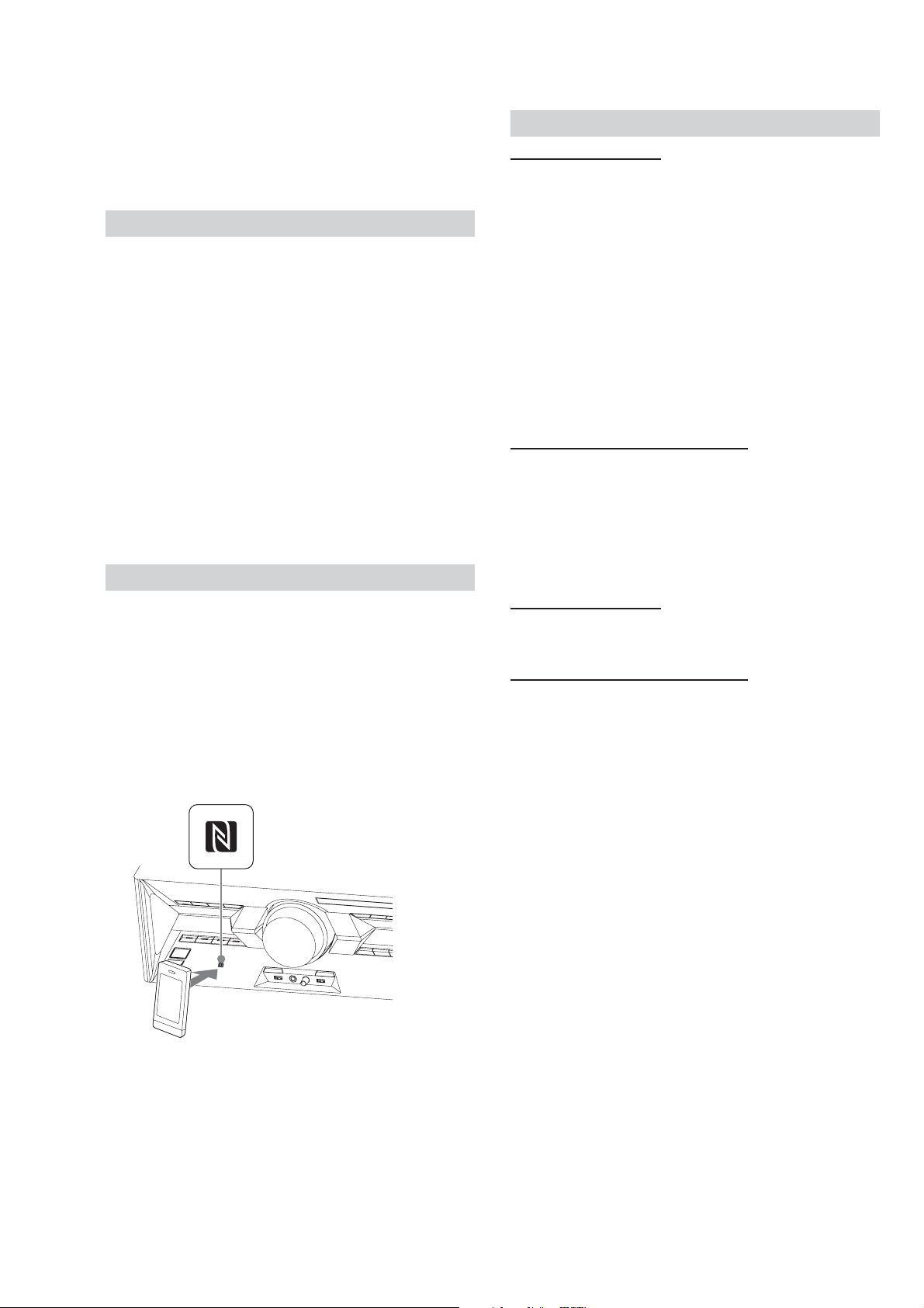
For an NFC-compatible smartphone
1. Press the [\/1] button to turn the power on.
Touch the smartphone to the N-Mark on the system to establish
the Bluetooth connection.
Start playback of an audio source on the smartphone. For
details on playback, refer to the operating instructions of your
smartphone.
\/1] button to turn the power on.
Bluetooth
device
Connecting with a smartphone by one touch (NFC)
Note: The operation in this mode must use a NFC-compatible smartphone
(Smartphones with a built-in NFC function [OS: Android 2.3.3 or
later, excluding Android 3.x])
1. Press the [\/1] button to turn the power on.
2. Download and install the app “NFC Easy Connect”.
Download the free Android app from Google Play by searching
for “NFC Easy Connect”.
3. Start the app “NFC Easy Connect” on the smartphone.
Make sure that the application screen is displayed.
4. Touch the smartphone to the N-Mark on the system until the
smartphone vibrates.
To disconnect the Bluetooth device
For a Bluetooth device
Press BLUETOOTH on the unit.
“BLUETOOTH” appears in the display panel.
For an NFC-compatible smartphone
Touch the smartphone to the N-Mark on the system again.
To erase all the pairing registration information perform
COLD RESET test mode (Refer page 14).
Complete the connection by following the instructions
displayed on the smartphone.
5. When pairing is completed and the Bluetooth connection is
established, the Bluetooth device name appears in the display
panel.
5
Page 6

HCD-SHAKE7
Note: Disassemble the unit in the order as shown below.
SET
2-1. SIDE-L PANEL ASSY, SIDE-R PANEL ASSY,
TOP PANEL
(Page 7)
2-2. BACK PANEL SECTION
(Page 8)
2-3. LOADING PANEL ASSY
(Page 8)
2-4. CDM90-DVBU202//M
(Page 9)
SECTION 2
DISASSEMBLY
2-5. FRONT PANEL SECTION
(Page 9)
2-6. MOTHERBOARD BOARD
(Page 10)
2-7. SWITCHING REGULATOR (SMG-1800)
(Page 11)
2-8. SERVICE OPTICAL DEVICE,
WIRE (FLAT TYPE)
(Page 12)
6
Page 7
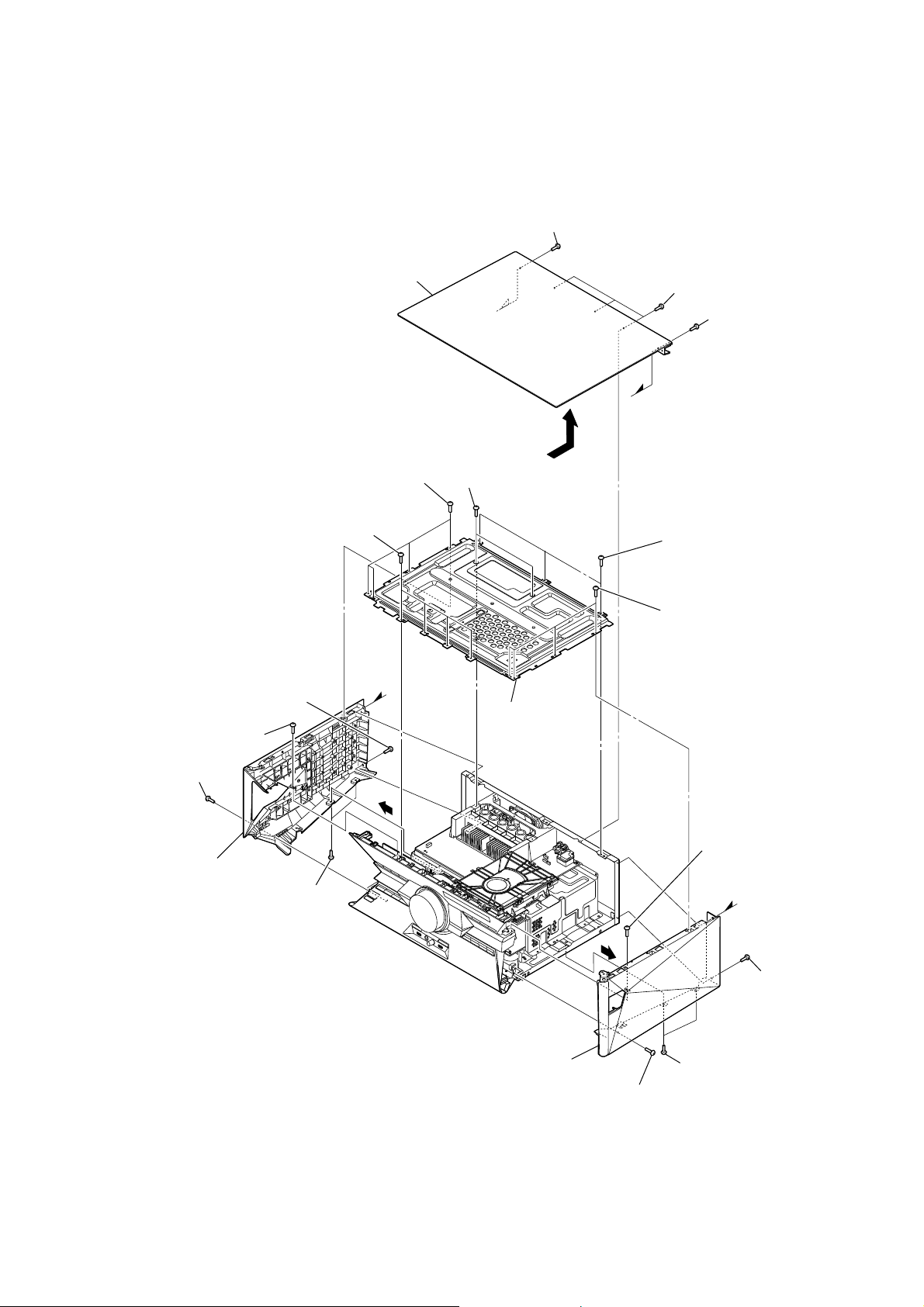
Note: Follow the disassembly procedure in the numerical order given.
2-1. SIDE-L PANEL ASSY, SIDE-R PANEL ASSY, TOP PANEL
2 one screw
(+BVTP 3 u 10)
HCD-SHAKE7
0 one screw
(+BVTP 3 u 8)
8 one screw
(+BVTP 3 u 10)
5 four screws
(+BVTP 3 u 8)
7 one screw
(+BVTP 3 u 10)
4 panel, top
5 four screws
(+BVTP 3 u 8)
A
qa
A
5 two screws
(+BVTP 3 u 8)
6 case, top
1 three screws
(+BVTP 3 u 10)
2 one screw
(+BVTP 3 u 10)
B
3
5 three screws
(+BVTP 3 u 8)
5 four screws
(+BVTP 3 u 8)
qs panel, side-L assy
9 two screws
(+BVTP 3 u 10)
qk panel, side-R assy
qj
qf one screw
(+BVTP 3 u 10)
qh one screw
(+BVTP 3 u 8)
B
qd one screw
(+BVTP 3 u 10)
qg two screws
(+BVTP 3 u 10)
7
Page 8
HCD-SHAKE7
2-2. BACK PANEL SECTION
1 CN1001 (2P)
2 CN1000 (2P)
6 two screws
(+BVTP 3 u 8)
5 five screws
(+BVTP 3 u 8)
4 three screws
(+BVTP 3 u 8)
3 three screws
(+BVTP 3 u 8)
2-3. LOADING PANEL ASSY
hole
– Side view –
Insert the clip etc.
processed to the
length of 8 cm or
more in the hole
on the side of the
chassis and push.
BD drive
7
8 back panel section
4 panel, loading assy
3 four claws
2
8 cm or more
Note:
8
tray
1 Insert the clip etc.
Push after it inserts it in this hole well.
– Top view –
Page 9
2-4. CDM90-DVBU202//M
HCD-SHAKE7
4 four screws
(+BVTP 3 u 8)
Note: When you install the BD
5 boss
drive (CDM90-DVBU202//M),
please match the position of
the boss two places.
1 wire (flat type) (24 core)
(CN305)
9 one screw
(+BVTP 3 u 8)
8 two screws
(+BVTP 3 u 8)
qa bracket, CDM
7 CDM90-DVBU202//M
3 wire (flat type) (5 core)
(CN306)
2 CN901 (6P)
6
0 one screw
(+BVTP 3 u 8)
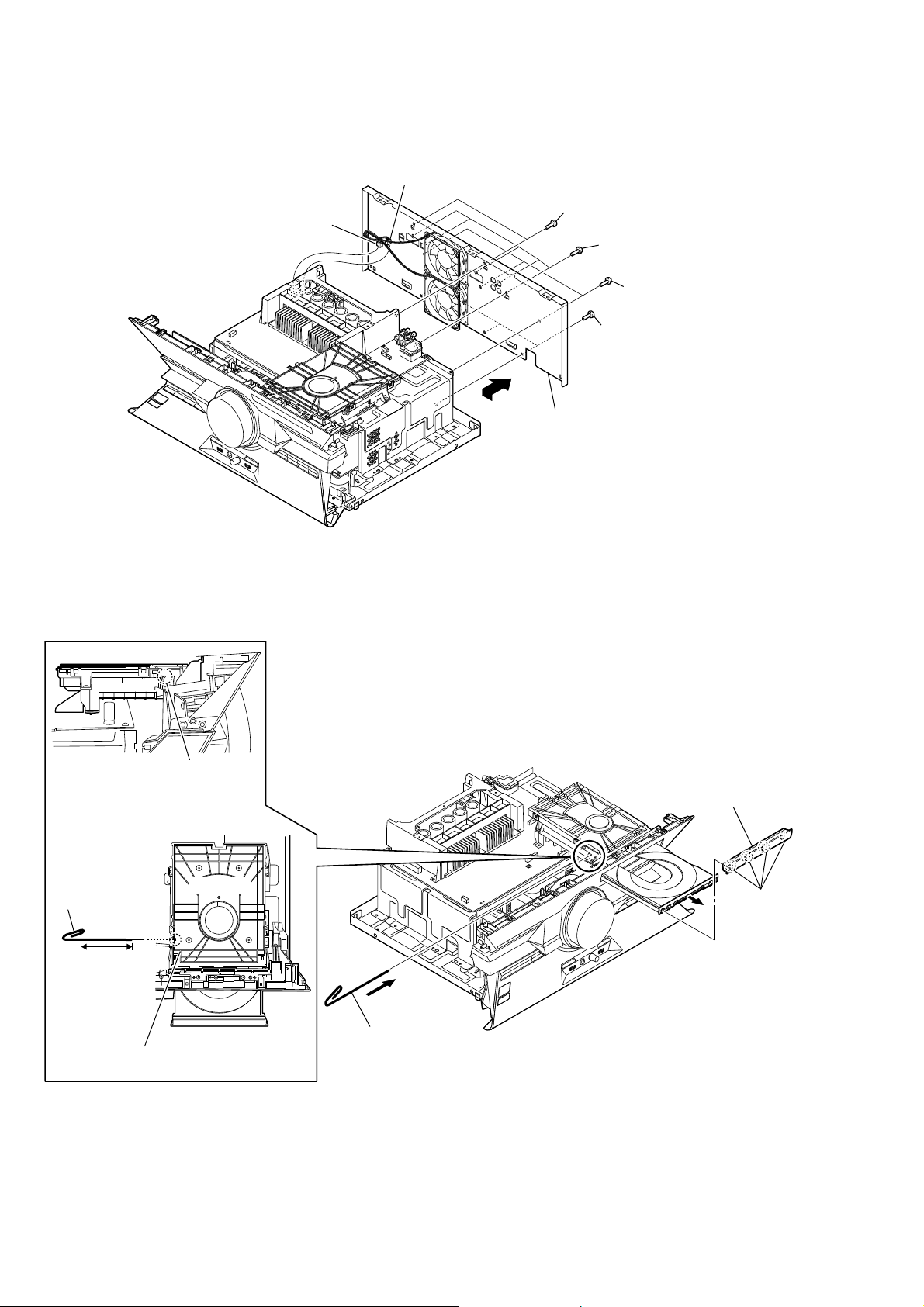
2-5. FRONT PANEL SECTION
8 front panel section
6 wire (flat type)
(8 core) (CN8)
2 wire (flat type)
(14 core) (CN10)
3 CN9 (4P)
7
4 wire (flat type)
(25 core) (CN12)
5 CN6 (10P)
1 six screws
(+BVTP 3 u 8)
9
Page 10

HCD-SHAKE7
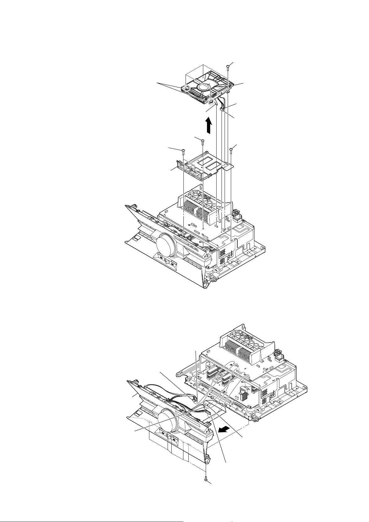
2-6. MOTHERBOARD BOARD
5 three screws
(+PTPWH 2.6 u L (DIA8.0))
3 two screws
(+BVTP 3 u 8)
8 three screws
(+BVTP 3 u 8)
1 CN1002 (9P)
2 CN1 (5P)
7 heat sink
6 thermal sheet
4 bracket, tunnel
8 two screws
(+BVTP 3 u 8)
8 two screws
(+BVTP 3 u 8)
9 MOTHERBOARD board
0
qa bracket, heat sink
10
Page 11
2-7. SWITCHING REGULATOR (SMG-1800)
5 nine screws
(+PWH 3 u 8 (SUMITITE))
HCD-SHAKE7
1 six screws
(+PWH 3 u 8 (SUMITITE))
2 sub chassis
6 REGULATOR, SWITCHING
(SMG-1800)
7 chassis
3 CN1 (2P)
4
11
Page 12

HCD-SHAKE7
2-8. SERVICE OPTICAL DEVICE, WIRE (FLAT TYPE)
Note 1 : Before disconnecting the wire (fl at type) (24 core) of optical pick-up block, solder the short-land.
2 chuck holder assy (T)
1 six claws
2 Solder the short-land.
Note 2: When assembling the optical pick-up block,
remove the solder of short-land after
connecting the wire (flat type) (24 core).
qa insulator
8 four insulator screws
qs service,
optical device
qa insulator
6 belt
3 Insert the thin
wire (clip etc.).
qd base, lo assy
4
5 tray
,QVWDOODWLRQRIZLUHIODWW\SHFRUHDQGZLUHIODWW\SHFRUH
This illustration sees the loading assy (T) from bottom side.
Note:
1 wire (flat type) (24 core)
loading assy (T)
0
9
7 connector
5 two claws
qg wire (flat type)
(5 core)
qa insulator
qj holder, FFC
qf tape
qk wire (flat type)
(24 core)
qh
loading assy (T)
– Bottom view –
5 three claws
12
terminal face
2 Through the hole
Under the guide
(Fold area)
3 Through the hole
6 holder, FFC
4
Fold
7 wire (flat type) (24 core)
9 tape
8 wire (flat type)
(5 core)
Under the guide
Page 13
SECTION 3
STORM TEST MODE
HCD-SHAKE7
[PANEL TEST MODE]
This mode is used to check the fl uorescent indicator tube, LEDs,
keys, [VOLUME / DJ CONTROL] jog, model, destination and
software version.
Procedure:
1. Press [ENTER] and [MUSIC] button simultaneously and hold
3 seconds.
2. All LEDs and segments in fl uorescent indicator tube are light-
ed up. All RGB LEDs are lighted up in white color.
3. When you want to enter to the software version display mode,
press [+ / ] button.
The model information appears on the fl uorescent indicator
tube.
• “STORM” is shown for SHAKE-7.
** If display shown information below, please proceed with
[MODEL & DEST WRITE MODE] to write model & destination.
• “STORM(T)” is shown for SHAKE-7.
Press [+ / ] button again to view the destination informa-
tion.
4. During the destination information display, press [+ / ]
button. Each time [+ / ] button is pressed, the fl uorescent
indicator tube shows the version of each category software in
the following sequence: SC, MTK, UI, PF, SYS, CD, CDMA,
CDMB, ST, TA, TAS, TM, BTM, BT, NFC, and return back to
model information display.
5. When [] button is pressed while the version numbers
are being displayed except model and destination, the
date of the software creation appears. When [] button
is pressed again, the display returns to the software version display.
6. Press [- / ] button, the key check mode is activated.
7. In the key check mode, the fl uorescent indicator tube displays
“K 0 V0”.
• Each time a button is pressed, “K” value increases.
However, once a button has been pressed, it is no longer taken into account.
• “V” value increases in the manner of 0, 1, 2, 3... if
[VOLUME / DJ CONTROL] knob is turned clockwise, or it decreases in the manner of 0, 9, 8, 7... if
[VOLUME / DJ CONTROL] knob is turned counterclockwise.
8. When [ENTER] button is pressed after all LEDs and segments
in fl uorescent indicator tube light up, alternate segments in
fl uorescent indicator tube and LEDs would light up, all RGB
LEDs would light up in red color. If you press [ENTER] button again, another half of alternate segments in fl uorescent in-
dicator tube and LEDs would light up, all RGB LEDs would
light up in green color. Pressing [ENTER] button again would
cause all segments in fl uorescent indicator tube and LEDs light
up, all RGB LEDs would light up in blue color. Pressing [ENTER] button again would turn off all segments in fl uorescent
indicator tube and all LEDs including RGB LEDs.
9. To release from this mode, press the buttons in the same manner as step 1, or disconnect the power cord.
[MODEL & DEST WRITE MODE]
This mode is used to set software model & destination.
This mode is only available when no permanent model & destination is stored.
Procedure:
1. Press [ENTER] and [FOOTBALL] button simultaneously and
hold for 5 seconds.
2. Fluorescent indicator tube display will show “M XXXXX”.
3. Press [+ / ] button to select the model based on the set’s
model.
Product Code F. Tube display
STORM “M STORM”
4. Press [ENTER] button.
5. Fluorescent indicator tube display will show “D XXXXX”.
6. Press [+ / ] button to select the destination based on the
set’s country.
Area Code Country F. Tube display
J1 Japan “D J”
JE1 Tourist “D JE”
U2/CA2 America, Canada “D NA”
CEL/CE1/
CE2
CEK U.K. “D CEK”
RU1/RU3 Russia “D RU”
AU1 Australia “D AU”
CN1 China “D CN”
E12 India, Pakistan, Morocco “D E12”
E3/E93/
SA2/E15
E4 Africa “D E12”
EA3 Saudi Arabia “D EA3”
HK1/
HK2/PL1/
SP1/SP2/
SP6/TH1
KR2 Korea “D KR”
TW2 Taiwan “D TW”
E2, E32,
E51, AR2
BR1 Brazil “D BR”
MX2,
MX4
7. Press [ENTER] button to confi rm the selection.
8. “RESET” appears on the fl uorescent indicator tube. After that,
the fl uorescent indicator tube becomes blank for a while, and
the system is reset.
9. Perform [PANEL TEST MODE] again to confi rm on the mod-
el & destination.
Europe (general) “D CE2”
Middle East, Africa
(South Africa), Iran
Hong Kong, Philippines,
Singapore, Malaysia,
Thailand
Latin America (general),
Chile, Peru, Argentina
Mexico “D MX”
“D E3”
“D ASIA”
“D LATIN”
13
Page 14

HCD-SHAKE7
[USER RESET]
The user reset clears all data including preset data stored in the data
fl ash to initial conditions exclude history mode data.
Procedure:
1. Press
2. Press [] and [LED COLOR] button simultaneously for 3
3. “RESET” appears on the fl uorescent indicator tube. After that,
[COLD RESET]
The cold reset clears all data including preset data stored in the
data fl ash to initial conditions included history mode data. Execute
this mode when returning the set to the customer.
Procedure:
1. Press
2. Press [] and [AUDIO IN] button simultaneously for 3
3. “COLD RESET” appears on the fl uorescent indicator tube.
[CD SHIP MODE (WITH MEMORY CLEAR)]
This mode moves the optical pick-up to the position durable to
vibration and clears all data including preset data stored in the data
fl ash to initial conditions during the next AC-In. Use this mode
when returning the set to the customer after repair.
Procedure:
1. Press \/1 button to turn on the system.
2. Select CD function.
3. Press [CD] and [SOUND FLASH] button simultaneously for 3
4. “MECHA LOCK” is displayed on the fl uorescent indicator
\/1 button to turn on the system.
seconds.
the fl uorescent indicator tube becomes blank for a while, and
the system is reset.
\/1 button to turn on the system.
seconds.
After that, the fl uorescent indicator tube becomes blank for a
while, and the system is reset.
seconds. The system turns off automatically.
tube and the CD ship mode is set.
[CDM AGING MODE]
This mode is used for CDM aging.
Procedure:
1. Press \/1 button to turn on the system.
2. Select CD function.
3. Open the disc tray, insert a disc and close the tray .
4. Press [CD] and [BASS BAZUCA] button simultaneously for 3
seconds.
5. The fl uorescent indicator tube displays Aging Display “AG
xxxx/yyyy”.
“xxxx” represents the error counter
(Maximum Value of “xxxx” = 9999)
“yyyy” represents the cycle counter
(Maximum Value of “yyyy” = 9999)
6. Press [+ / ] or [- / ] to search for Aging History Error
Display
The fl uorescent indicator tube displays “Mx E1E2E3E4”.
x: error history number
E1: Loading sequence JCP high
E2: Loading sequence JCP low
E3: Loading operation JCP
E4: Cam position operation JCP
7. Press [ENTER] to Aging Display
To release from this mode, press [\/1] button.
[HISTORY MODE]
This mode is used to check important data stored in the system
when PROTECTOR happen.
Procedure:
1. During demo mode, press [ENTER] and [LED PATTERN] for
5 seconds to mode in to history mode.
2.
Press the [ .m / TUNING-] or [M > / TUNING+]
button to check history data stored.
[CD TRAY LOCK MODE]
This mode let you lock the disc tray. When this mode is activated,
the disc tray will not open when [Z OPEN/CLOSE] button is
pressed. The message “LOCKED” will be displayed on the fl uo-
rescent indicator tube. This mode only applied when there is disc
on the tray.
Procedure:
1. Press \/1 button to turn on the system.
2. Select CD function.
3. Press [] and [ENTER] button simultaneously and hold down
until “LOCKED” or “UNLOCKED” displayed on the fl uores-
cent indicator tube (around 5 seconds).
14
Page 15
Display Item
PROCOUNT
PROTYPE
※※
※※※※
HCD-SHAKE7
Protector Count
Protector T ype (refer PROTECTOR KIND CHECK TEST MODE)
Protector type Protector Error Code
AMPL E01
PWR2 E03
SPK E04
TEMP E05
FAN E06
T1
T2
FUNC
VOL
ATT
EQ LOW
EQ MI D
EQ HIGH
VACS
APVACS
SW
SURR
DJ
BAZUCA
To release from this mode, press [\/1] button.
[PROTECT KIND CHECK TEST MODE]
This mode is used to check types of protect occurred during
protector on.
Procedure:
1. During protection on, fl uorescent indicator tube shows blinking
message “PROTECT EXX” where “EXX” represent the error
code.
2. Press [] and [- / ] button simultaneously.
3. Fluorescent indicator tube display will toggle between
“PROTECT” message and protector kind message display.
Below table explains on protector kind.
Error
Code
※※※※※H※※
※※※※※H※※
※※※※※※※
※※※
※※※
※※※
※※※
※※※
※※※
※※※
※※※※※※ ※※
※※※
Protector
Message
Description
※※
※※
Single Power On Time
M
Total Power On Time
M
Input Function
Volume
Actual Attenuation
Low EQ Level
Mid EQ Level
High EQ Level
VACS Level
AP VACS Level
Subwoofer Setting
Surround Setting
DJ Effect Setting
Bass Bazuca Setting
To release from this mode:
Press [] and [- / ] button simultaneously again or unplug &
re-plug in the power cord.
If speaker does not have output even if the set status is not in
PROTECT mode, the following defect might be possible:
Defects Possible cause
RESET defect Reset signal status from micom is not ‘H’.
If the PROTECT mode is “POWER SUPPLY”, there is
possibility of unusual power supply of any of the AMP IC or
Pre-amplifi er.
E01 “AMP OCP” The over current condition to
MOSFET occurs by defect of
MOSFET or defect of PS output
line.
E03 “POWER
SUPPLY”
E04 “DC DETECT” DC appears in SP terminal by
E05 “THERMISTOR” Unusual heat up of MOSFET by
E06 “F AN BLOCK” Defect of DC F AN and DC FAN
Defect of power supply circuit
to AMP
defect of AMP IC and MOSFET.
improper assembly of heat sink,
destruction of MOSFET etc.
driver circuit
15
Page 16
HCD-SHAKE7
SECTION 4
ELECTRICAL CHECK
TUNER SECTION
FM AUTO STOP CHECK
set
Procedure:
1. Turn the power on.
2. Input the following signal from Signal Generator to FM
antenna input directly.
Carrier frequency : A = 87.5 MHz, B = 98 MHz, C = 108 MHz
Deviation : 75 kHz
Modulation : 1 kHz
ANT input : 35 dBu (EMF)
Note: Please use 75 ohm “coaxial cable” to connect SG and the
set. You cannot use video cable for checking.
Please use SG whose output impedance is 75 ohm.
0 dB = 1 ȝV
signal
generator
+
75
–
3. Set to FM tuner function and scan the input FM signal with
automatic scanning.
4. Confi rm that input Frequency of A, B and C detected and
automatic scanning stops.
The stop of automatic scanning means “The station signal is
received in good condition”.
16
Page 17
SECTION 5
TROUBLESHOOTING
HCD-SHAKE7
Checks circumference circuit for IC651, IC652 of DMB Mount.
If there are no problems, checks circumference circuit for
REGIC of Main mount.
Checks circumference circuit for SL+/SL- of IC801.
Checks circumference circuit of IC501 FMO Signal.
No
Does it output the power voltage of 3.3V and 1.2V?
Checks 3.3V REG of DMB Mount and 1.8V REG.
No
No
Yes
Yes
Does it output the signal?
Checks CN801 SL+/SL- signal.
The Sled motor has a problem.
Replaces BU.
Checks circumference circuit for SP+/SP of IC801.
Checks circumference circuit of IC501 DMO Signal.
No
Yes
The Spindle motor has a problem.
Does it output the signal?
Checks CN801 SP+/SP- signal.
No
Replaces BU.
Checks circumference circuit of IC501 FOO Signal.
Checks circumference circuit for FCS+/FCS- of IC801
No
Yes
The Optical pickup has a problem.
Does it output the signal?
Checks CN501 FCS+/FCS- signal.
No
Replaces BU.
Yes
REMOVE TOP PANEL
REMOVE SIDE PANEL
TURN ON
TRAY IN
Does Optical pickup move to inner circumference?
Optical Block Diagnosis Flow (1/2)
(Visual check)
Yes
Does Spindle motor rotate?
(Visual check)
Yes
Does Optical pickup do focus search?
(Visual check)
A
17
Page 18

HCD-SHAKE7
Checks circumference circuit of Q605 or Q606.
Checks circumference circuit of IC501 LDO1 and LDO2.
No
Yes
The Optical pickup has a problems.
Does it output 2V when laser become luminous?
Checks JL602 (LD650) signal.
Checks JL606 (LD780) signal.
No
Replaces BU.
If it is not up to standard,
Lens cleaning is performed.
No
Replaces BU if it is not up to standard.
No
Yes
Is output level of RF signal (CN507 6pin) up to standard?
Yes
RF Level = 1.05 ±0.45 Vpp
Test CD:YEDS-18
No
The Optical pickup has a problems.
Replaces BU.
A
Optical Block Diagnosis Flow (2/2)
Does laser diode become luminous ?
18
Yes
(Visual check)
Yes
DISC IN
Yes
RF Level = 1.05 ±0.45 Vpp
Test CD:YEDS-18
Is output level of RF signal (CN507 6pin) up to standard?
Yes
Is there no problem with Long term Aging Test (60min)?
Confirms that there is no sound skip.
END
Page 19
HCD-SHAKE7
Reinserts the cable or Exchanges.
If there are no problems, Checks P-CON
Output of MOTHERBOARD Board side.
Reinserts the cable or Exchanges.
If there are no problems, Checks output of
Switching regulator Board.
Reinserts the cable or Exchanges.
No
Is the power voltage OK?
No
No
Yes
Checks 13.5V output of CN1 5pin.
Is the power voltage OK?
No
Yes
Checks 3V output of CN1 1pin(V-CON)
If there are no problems, Checks Output of
V-CON Output of MOTHERBOARD Board side.
Reinserts the cable or Exchanges.
If there are no problems, Checks output of
Switching regulator Board.
No
Yes
Is the power voltage OK?
Checks 56.5V output of CN1002 6pin (+VH)
and -56.5V output of CN1002 1pin (-VH).
Is the power voltage OK?
Checks circumference circuit of REG IC1014.
If there are no problems, exchanges IC1014.
No
Yes
Checks OUT terminal -17.5V output of REG IC1014
Yes
Is it shorted out?
Or, Checks GND and OUT Terminal with Tester.
Checks circumference circuit of REG IC1015.
If there are no problems, exchanges IC1015.
No
Checks OUT terminal -29.5V output of REG IC1015
Or, Checks GND and OUT Terminal with Tester.
Is it shorted out?
Checks circumference circuit of REG IC1016.
If there are no problems, exchanges IC1016.
No
Yes
Checks OUT terminal -44.5V output of REG IC1016
Yes
B
Or, Checks GND and OUT Terminal with Tester.
Is it shorted out?
Yes
PLAY MUSIC
MOTHERBOARD Mount Diagnosis Flow (1/2)
Yes
Is there audio output from MOTHERBOARD Board? Checks 3V output of CN1 2pin(P-CON).
A
19
Page 20
HCD-SHAKE7
Checks circumference circuit of REG IC1006.
If there are no problems, exchanges IC1006.
No
B
Checks OUT Terminal 5V output of REG IC1006 or,
Checks GND and OUT Terminal with Tester.
Is it shorted out?
Checks circumference circuit of REG IC1007.
If there are no problems, exchanges IC1007.
No
Yes
Checks OUT Terminal -5V output of REG IC1007 or,
Yes
Checks GND and OUT Terminal with Tester.
Is it shorted out?
Replaces MOTHERBOARD Board
No
Leave MOTHERBOARD Mount to a state of it only
and, checks Power Audio Driver(MOS FET) with Tester.
Replaces MOTHERBOARD Board
No
Yes
Is it shorted out? (Refer to Page 21.)
Assembles into the unit again then, checks
Yes
whether there is the audio output from
MOTHERBOARD Board.
A
MOTHERBOARD Mount Diagnosis Flow (2/2)
20
END
Page 21
JL204
JL208
JL276
C100
C98
C99
JL262
JL209
JL281
C115
JL207
JL199
R27
JL200
D4
D3
D2
Q1009, Q1045
R25
R24
C116
JL201
JL206
JL205
JL198
C221
JL238
JL1064
JL1067
JL1072
JL1066
JL1069
JL1070
JL1068
JL1075
JL1071
R217
JL88
JL80
JL664
JL665
JL657
JL658
JL195
JL194
JL196
JL197
CL2
JL280
B2E2C1
B1C2E1
R
LED
CN4
SPEAKER
MOSFET Confi rmation for MOTHERBOARD Mount
JL214
JL215
C220
C219
C118
C117
JL1063
JL241
JL1135
JL1132
JL1091
JL1093
JL1074
JL1065
JL1149
JL225
JL1148
JL1012
R1435
JL1062
JL1050
JL1020
JL1145
JL1131
R1375
JL1109
R1378
JL1119
JL1108
R1377
R1376
R1371
R1374
JL1118
R1367
R1365
JL1104
JL1111
R1379
R1380
JL1073
JL1115
JL1110
JL1055
R1359
R1362
JL1116
R1368
R1363
R1370
R1372
C1175
JL1103
C1174
JL1107
JL1094
JL1057
JL1113
JL1054
JL1112
Test e r
C1167
C1166
JL1114
R1382
R1361
R1360
R1381
JL1102
R1364
R1373
R1369
C1172
JL1105
JL674
JL285
JL1117
C1173
JL86
JL87
JL84
JL85
CL329
JL671
JL1016
JL1015
JL1014
JL1086
Tester
JL1037
JL1036
JL1147
R1452
R1366
C1377
JL81
JL82
JL83
CL328
CL327
CL330
CL331
CL332
CL336
CL337
CL309
C311
C337
R363
C321
C322
D306
HCD-SHAKE7
JL138
C217
C218
JL1019
JL1137
R1431
R1145
Q1017
JL1120
Q1048
JL1078
R1177
JL1081
Tester
JL321
JL319
JL320
JL325
JL324
JL332
JL327
JL336
C916
21
30
29
R906
C326
C303
JL903
JL905
JL906
D1002
JL1125
JL1123
R1129
JL1087
R1170
R1178
JL1080
R1052
JL1010
JL1122
D1000
JL1121
JL1143
JL1089
R1130
R1172
R1054
Tester Tester
JL323
JL331
JL337
JL338
C915
JL901
C907
JL902
JL904
C908
JL304
R1127
R1179
R1053
JL1082
D1001
JL1126
JL1088
R1171
JL1124
C799
C792
R828
R824
JL333
JL661
JL175
JL227
JL341
JL339
JL340
14
R927
SL901
SL902
SL903
SL904
R1401
Q1051
R1433
R1402
R1434
R1182
R1181
D1003
R1084
Q1049
R1126
R1077
R1058
C1306
JL1084
R1056
JL1079
C1030
C1033
R1081
C1347
C1346
JL1083
JL1077
JL1085
R1131
R1055
C133
C135
JL1130
JL1127
JL1129
D1006
C1196
C1241
JL1038
R1210
JL1041
JL1035
R1118
R1087
JL1128
R1183
IC1010
R1088
R1184
C1244
JL1030
R1119
JL1042
R1211
C1307
JL1047
R1078
C1197
C1318
R1468
C1198
R1128
R1079
R1161
JL1040
R1191
C1242
JL1044
R1406
IC1011
R1466
R1404
C1245
R1467
JL1045
R1193
JL1049
R1162
C1205
R1470
R1471
JL1142
C1319
C1206
R1080
R1192
JL1039
JL1043
C1031
C1243
R1160
IC1012
R1207
R1209
R1163
C1246
R1194
JL1046
C1032
R1082
JL1048
C1199
C805
C683
R653
C740
C668
R812
R814
C728
C769
C768
R816
JL655
JL654
R750
R751
R817
JL169
JL178
JL252
JL75
R155
R72
R139
JL72
JL70
R166
JL74
R127
R154
R136
JL73
C82
R133
R165
R132
R125
JL34
C134
Tester Tester
JL1076
JL1018
JL1133
JL1146
C1368
C1372
C1374
C1376
Tester
C1054
JL1099
C1055
C1047
JL1097
C1049
C1056
JL1100
C1057
Tester
C1046
JL1096
C1050
C1058
JL1101
C1059
C1048
Tester
JL1098
C1051
JL1017
R1437
C1367
R1440
C1369
C1370
R1443
C1371
C1373
R1446
R1449
C1375
C1378
Tester Tester
JL318
JL329
JL322
JL326
JL328
JL330
JL334
JL335
C921
C918
CL334
IC902
CL326
R378
C919
R916
22
2815
1
78
C920
C922
R919
R908
C302
JL315
JL312
JL313
R349
R350
JL316
JL314
C305
C304
CL333
C349
R305
C365
C308
C313
C348
C339
C364
C351
R366
C338
C352
C335
C309
C336
C332
C331
R324
C334
R383
R368
R352
R353
CL324
D305
CL325
D300
C211
C210
JL1022
JL1021
E
Q1007
JL182
JL168
R3
JL1011
JL1136
C1192
C1320
Q1045
R1421
R1234
R1264
R1225
C1379R1469
R1089
R1090
R1092
C806
JL145
JL237
R1422
C1321
JL148
C1182
C746
JL1007
C1185
JL1031
R1227
R1265
R1231
JL1034
C1188
R1091
C1380
JL1032
R1226
R1266
R1230
JL1033
JL76
C144
R655
JL146
JL1003
JL1002
C745
R654
C1184
JL136
C1322
R1423
R1295
R1296
Q1009
R1424
C1323
C1189
JL147
JL1139
C140
R177
C91
C89
JL187
JL188
C138
R175
C90
JL186
JL189
JL184
JL124
JL103
JL663
R820
JL660
JL102
JL191
JL11
R130
JL275
JL137
JL283
JL135
JL139
JL141
JL142
JL144
JL176
JL151
JL152
JL149
JL154
JL150
JL177
JL158
JL181
JL180
JL157
JL155
JL179
JL160
JL156
JL659
R219
C21
R98
R157
C22
C23
C87
R195
IC12
C24
R196
R158
R99
R106
C25
JL282
JL224
JL173 JL174
JL172
JL92
JL662
JL93
JL127
JL131
JL213
JL278
JL134
D9
KA
JL132
JL125
JL130
JL162
JL128
JL126
JL226
JL161
JL121
JL118
JL120
JL123
JL190
R44
C94
C28
R167
R173
R171
R172
R1
JL257
JL279
JL114
JL113
JL112
JL111
JL110
JL109
JL273
JL119
JL117
R32
JL165
JL129
JL212
JL164
JL163
JL104
JL101
JL100
JL105
JL99
JL122
JL115
JL170
JL116
JL108
JL107
JL277
JL271
JL272
JL193
JL133
JL106
JL97
JL90
JL94
JL91
JL98
JL95JL96
R33
JL89
JL284
<Note>
Please check each channel’s resistance value for the Coil’s terminal and Capacitor’s + and – terminal.
These terminal is equal to resistance value for POWER AUDIO DRIVER terminal.
21
Page 22
HCD-SHAKE7
• Circuit Boards Location
SWITCHING REGULATOR (SMG-1800)
SECTION 6
DIAGRAMS
MOTHERBOARD board
BLUETOOTH module
BUTTON_L board
RGB BAR_L board
RC-S801/A (WW)
MS-476 board
VOLUME board
MIC SUPPORT board
BUTTON_R board
USB board
MIC board
RGB BAR_R board
22
DISPLAY board
Page 23
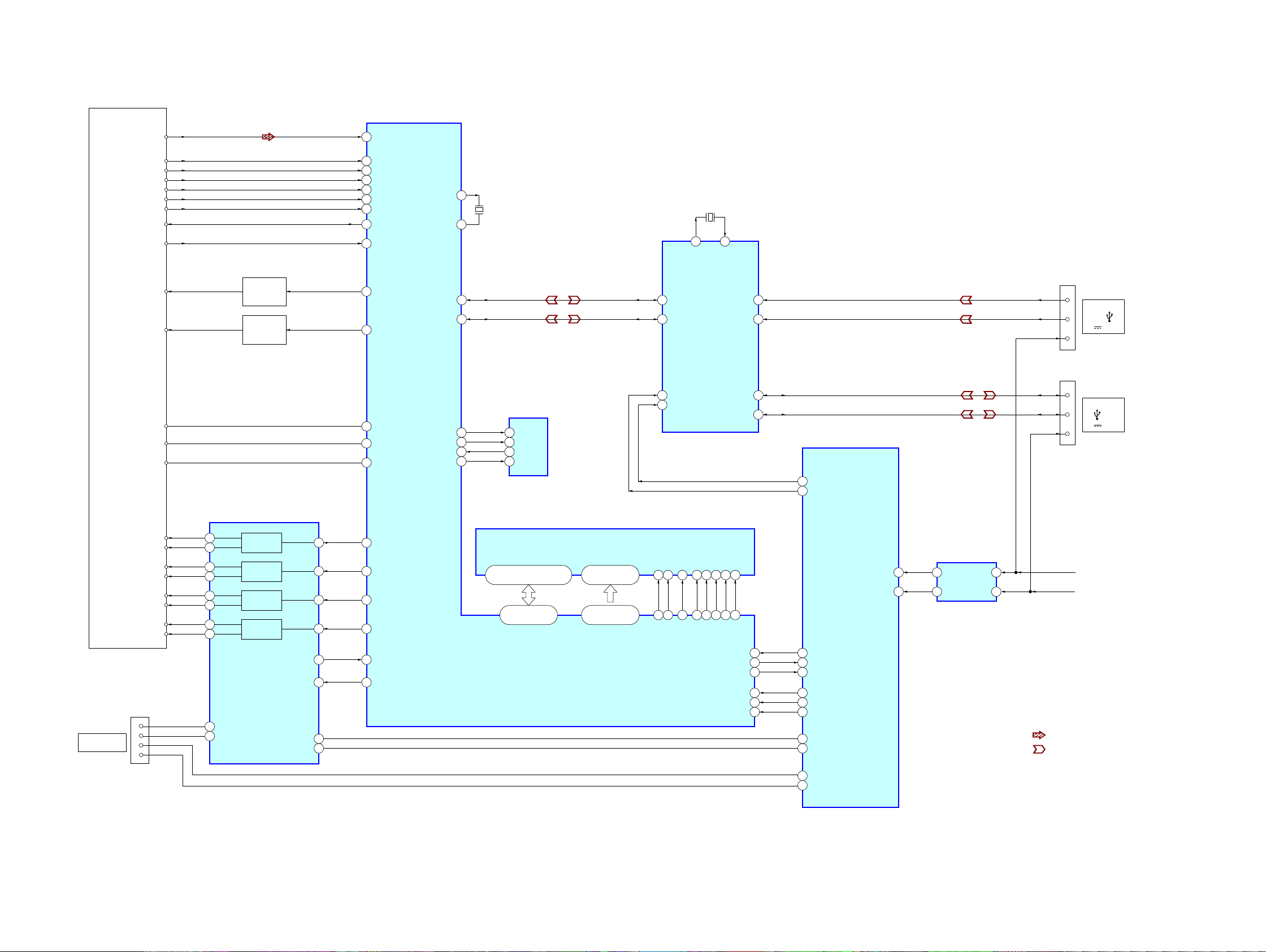
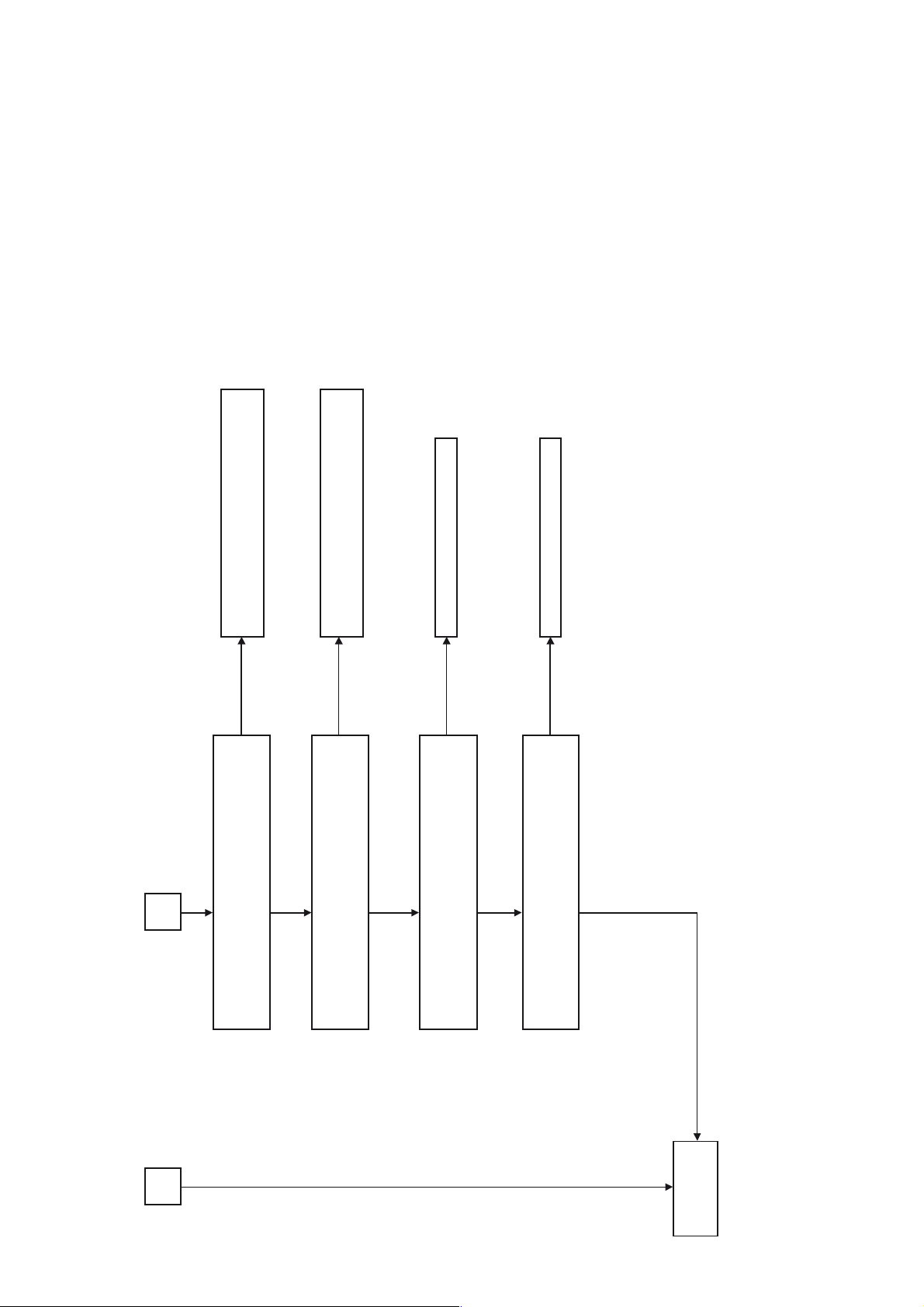
6-1. BLOCK DIAGRAM - RS SERVO, USB Section -
HCD-SHAKE7
CMS-S76RFS7G
(LO:DVD,HI:CD)MSW
CONNECT TO
MS-476 BOARD
DEVICE,
OPTICAL
RF
VOA/A
VOB/B
VOC/C
VOD/D
VC
PD
VR(780)
VR(650)
FCS+
FCS–
TRK+
TRK–
SL+ 17
SL– 18
SP+ 11
SP– 12
CN306
LOAD-
1
LOAD+
2
TRAY-IN
3
TRAY-OUT
5
123
RFIP
RF_C1
128
RF_B
127
RF_A
RF_D2
RF_F4VOE/E+G
RF_E3VOF/F+H
10
V20
MDI1
13
AUTO
POWER CTRL
Q902
AUTO
POWER CTRL
Q901
5CH SYSTEM
MOTOR DRIVER
IC902
14
13
16
15
9
10
VOTRVOTR+
FOCUS
COIL DRIVER
FOCUS
COIL DRIVER
FOCUS
COIL DRIVER
FOCUS
COIL DRIVER
BIAS
MUTE
FWD
REV
1
4
23
26
27
6
7
LDO114LD(780)
LDO215LD(650)
CD RF AMP
FOCUS/TRACKING ERROR AMP
CD SYSTEM PROCESSOR
DIGITAL SERVO PROCESSOR
MSW23
CD_VR19
DVD_VR20
FOO22
DMO17
FMO18
TRO21
V14/VREF011
45
MUTE28
IC306
(1/2)
XTALO
XTALI
USB_DP 25
USB_DM 24
SF_CS#
SF_DO
SF_DI
SF_CK
8
X301
27MHz
7
USBUP_DP
31
USBUP_DM
30
EEPROM
IC305
_CS
30
31
32
33
1
SO
2
SI
5
SCK
6
DG0, DQ1 – DQ15
2, 4, 5, 7, 8, 10, 11, 13, 42,
44, 45, 47, 48, 50, 51, 53
52 – 55, 57 – 60,
69 - 62
RD0 – RD15
64M SDRAM
IC304
A0 – A11
23 – 26,
29 – 34, 22, 35
89 - 92, 79 - 74,
88, 73
RA0 – RA11
VBUS_DET27
RESET_N26
20
21
85
86
BA0 BA0
BA1 BA1
X2
24MHz
32
XTAL2
USB CONTROLLER
IC9
38
15
39
18
72
61
70
83
RCLK CLK
DQM0 LDQM
DQM1 UDQM
33
XTAL1/CLKIN
17
82
RAS# RAS
16
80
CAS# CAS
RWE# WE
IFSDI 40
IFSDO 35
IFSCK 34
PRST#
IFCS# 42
IFBSY 41
CN2201
3
VBUS
VBUS
D+
D-
D+
D-
2
1
CN2202
3
2
1
PLAY
A
9 P$
REC/PLAY
B
9 P$
USB-A+5V
USB-B+5V
2USBDN1_DP
1USBDN1_DM
4USBDN2_DP
3USBDN2_DM
88
O-HUB-RESET
87
O-HUB-VBUS-DETECT
SYSTEM
CONTROLLER
IC11 (1/4)
/I-HUB-OC-USB-B
45
O-MTK-SDO
46
I-MTK-SDI
47
I-MTK-CLK
38
O-MTK-RESET55
56
I-MTK-XIFCS
57
O-MTK-BUSY
85
86/I-HUB-OC-USB-A
1
COMPARATOR
7
USB
IC12
3
5
6LJQDOSDWK
O-CD-MOTOR +
58
O-CD-MOTOR -
59
: CD PLAY
: USB
5FKLVRPLWWHGGXHWR
I-CDM-SW-A63
I-CDM-SW-B64
VDPHDV/FK
HCD-SHAKE7
2323
Page 24
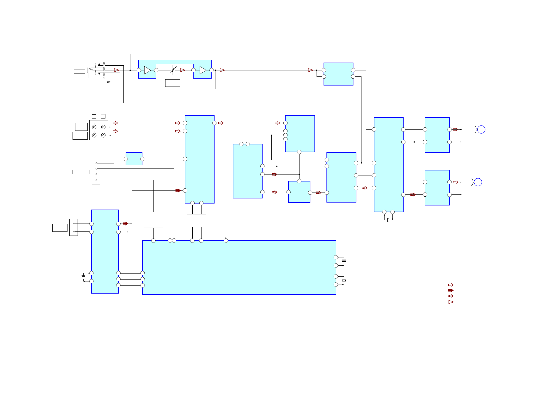
HCD-SHAKE7
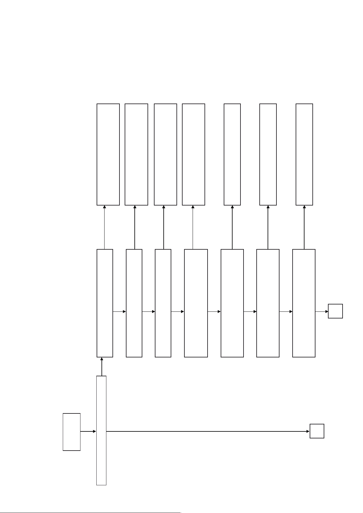
6-2. BLOCK DIAGRAM - MAIN Section -
MIC DETECT
Q2301, Q2302
J2301
MIC IN
MIC AMP
IC2301
RV2301
MIC VOL
MIN MAX
STEREO A/D
CONVERTER
IC654
VINL
1375
13
VINR
14
DOUT
BCK
9
8
ANTENNA
FM/AM
J651
AUDIO IN
PC/GAME
AUDIO IN
TV/DVD/SAT
BLUETOOTH
CN7
2
3
R
L
R-CH
R-CH
BLUETOOTH AMP.
IC13
CN10
LCH_P
4
UART_TX
8
UART_RX
9
3.3V
12
FM DRIVER
(FM RECEIVER)
IC3
413
ARF1 L OUT
R OUT
12
R-CH
ARF2
5
13
BLUETOOTH
CONTROL
POWER
Q9, Q15
21
STEREO A/D
SIGNAL SELECTOR
IC661
3
Y1
5
Y3
4
Y0
1
Y2
2
A
9B10
ANALOG
SELECTOR
Q652
33
34
51
Y
112
117
ACLK
ALRCK
113
ABCK
106
ADIN
118
ASDATA0
CD RF AMP
FOCUS/TRACKING ERROR AMP
CD SYSTEM PROCESSOR
DIGITAL SERVO PROCESSOR
IC306
(2/2)
52
91
CONVERTER
IC655
VINL
13
SCKI
6
LRCK
7
BCK
8
B
2
SIGNAL SELECTOR
IC664
9
1
A
DOUT
AUDIO DSP
IC656
SDIN2
12
LRCKI
6
BCKI
5
5
Y
SDIN
4
ASYNCHRONOUS
SAMPLE RATE
CONVERTER
IC653
BCKO
LRCKO
SDOUT
25
24
23
22
19
11
SCLKOUT1
LRCK
SDIN1
XTALO
4
X651
12.288MHz
SDOUT1
SCLKOUT2
SDOUT2
XTALI
3
27
23
26
STEREO D/A
CONVERTER
DATA
2
BCK
1
STEREO D/A
CONVERTER
BCK
1
DATA
2
IC651
IC652
VOUTL
VOUTR
VOUTL
VOUTR
7
8
FRONT-L
R-CH
A
SECTION
(Page 25)
AMP
AMP
7
8
SW-L
R-CH
B
SECTION
(Page 25)
HCD-SHAKE7
X3
12MHz
O-BT-ON
IIC/RDSI
DA
11
CK
8
6
28
27
43
I-ST-DATA
I-ST-CLK
I-ST-RDS
16
X1
X2
17
I-BT-RXD
O-BT-TXD
O-ANALOG-ASEL
O-ANALOG-BSEL
I-MIC-DETECT
SYSTEM CONTROLLER
IC11 (2/4)
I-Xin
O-XC-OUT
I-X-CIN
11O-Xout
13
9
8
X4
8MHz
X1
32.768kHz
6LJQDOSDWK
: AUDIO
: TUNER (FM/AM)
: CD PLAY
: MIC
5FKLVRPLWWHGGXHWR
VDPHDV/FK
2424
Page 25
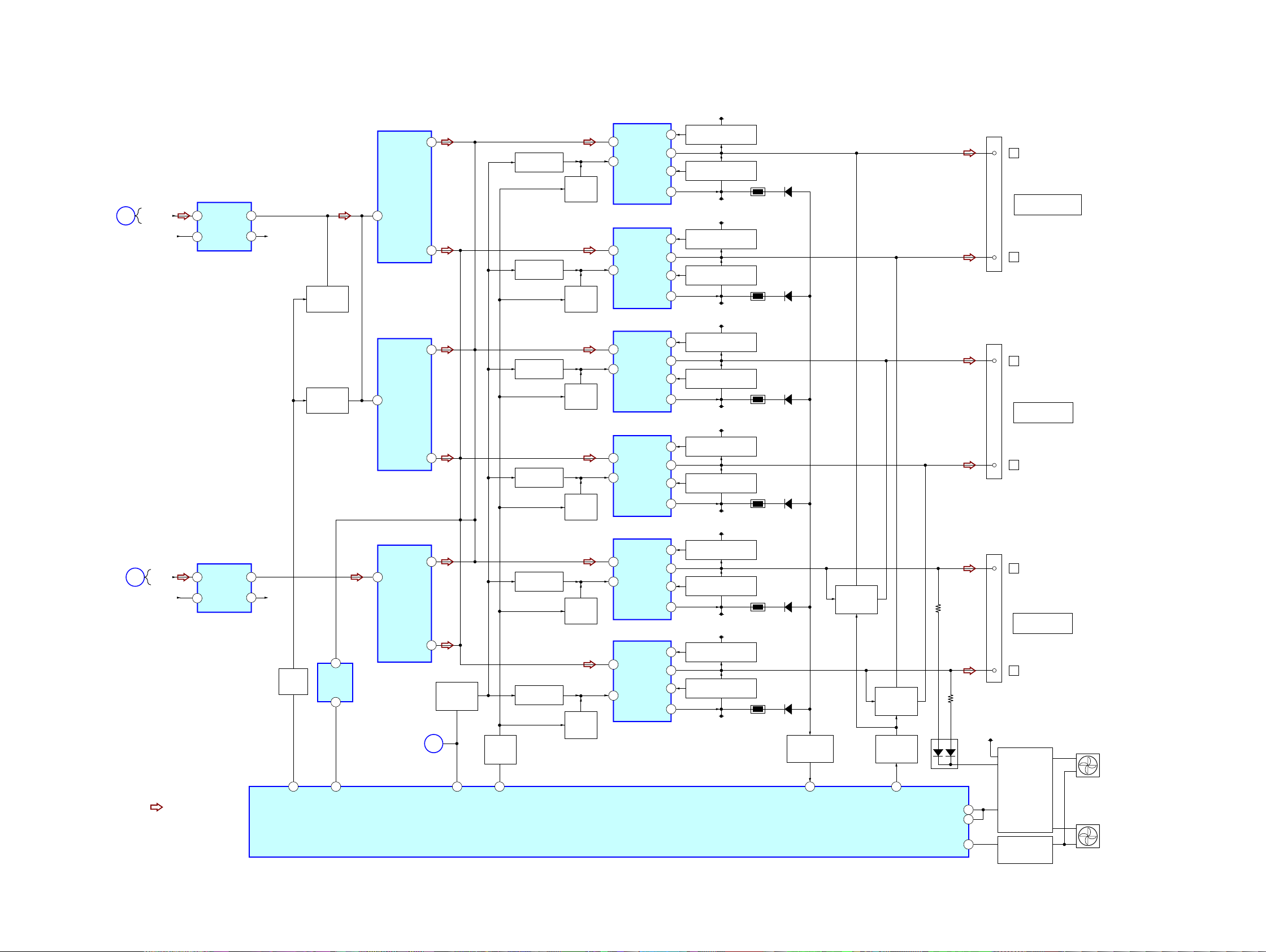
6-3. BLOCK DIAGRAM - AMP Section -
HCD-SHAKE7
MAIN
SECTION
(Page 24)
MAIN
SECTION
(Page 24)
FRONT-L
A
SW-L
B
6LJQDOSDWK
: AUDIO
5FKLVRPLWWHGGXHWR
VDPHDV/FK
OP AMP
IC1012
1
AOUT
RESET SWITCH
Q1012
OP AMP
IC658
+
3
+
5
OP AMP
+
3
+
5
IC660
OUT
OUT
OUT
OUT
1
7
R-CHR-CH
MUTE
PROTECTION
Q1009
MUTE
PROTECTION
Q1045
1
7
R-CHR-CH
MUTE
SWITCH
Q6
7
OP AMP
IC1008
5
INA+
3
7
BOUT
RESET SWITCH
Q1013
OP AMP
IC1011
1
AOUT
RESET SWITCH
Q1010
INA+
3
7
BOUT
RESET SWITCH
Q1015
OP AMP
IC1010
1
AOUT
INA+
3
7
BOUT
AMP RESET
SWITCH
Q1017
RESET SWITCH
Q1011
RESET SWITCH
Q1014
PANEL,
49
O-FRONT-MUTE
20
O-DAMP-CLK
POWER SUPPLY
SECTION
(Page 26)
C
73
O-DAMP-RESET
AMP
SWITCH
Q1048
I-DAMP-OCP
AMP
SWITCH
Q1024
AMP
SWITCH
Q1026
AMP
SWITCH
Q1023
AMP
SWITCH
Q1025
AMP
SWITCH
Q1019
AMP
SWITCH
Q1020
SYSTEM CONTROLLER
IC11 (3/4)
POWER AMP
3
IN
CSD
5
POWER AMP
3
IN
CSD
5
POWER AMP
3
IN
CSD
5
POWER AMP
3
IN
CSD
5
POWER AMP
3
IN
CSD
5
POWER AMP
3
IN
CSD
5
IC1000
IC1005
IC1001
IC1003
IC1002
IC1004
COM
COM
COM
COM
COM
COM
14
HO
13
VS
11
LO
10
14
HO
13
VS
11
LO
10
14
HO
13
VS
11
LO
10
14
HO
13
VS
11
LO
10
14
HO
13
VS
11
LO
10
14
HO
13
VS
11
LO
10
+53V
DIGITAL AUDIO MOSFET
Q1041
DIGITAL AUDIO MOSFET
Q1042
-53V
+53V
DIGITAL AUDIO MOSFET
Q1033
DIGITAL AUDIO MOSFET
Q1038
-53V
+53V
DIGITAL AUDIO MOSFET
Q1040
DIGITAL AUDIO MOSFET
Q1043
-53V
+53V
DIGITAL AUDIO MOSFET
Q1035
DIGITAL AUDIO MOSFET
Q1036
-53V
+53V
DIGITAL AUDIO MOSFET
Q1039
DIGITAL AUDIO MOSFET
Q1044
-53V
+53V
DIGITAL AUDIO MOSFET
Q1034
DIGITAL AUDIO MOSFET
Q1037
-53V
TH1001 D1001
TH1005 D1001
TH1002 D1000
TH1003 D1000
TH1000 D1002
TH1004 D1002
THERMISTOR
PROTECTION
Q1007, Q1022
7072
/I-THERMISTOR-DET
DC DETECT
SWITCH
Q1005, Q1055
DC DETECT
SWITCH
Q1004, Q1052
DC DETECT
SWITCH
Q1021, Q1047
71
/I-DC-DET
D1005
O-FAN-PWM
I-FAN-SPEED
/I-FAN-BLOCK-DET
TB1000
+
L
TWEETERS/WOOFERS
,03('$1&(86(ȍ
-
R
TB1001
+
L
MID SPEAKERS
,03('$1&(86(ȍ
R
TB1002
+
L
SUBWOOFERS
,03('$1&(86(ȍ
-
R
13V
FAN DRIVER
Q1030, Q1032,
24
69
68
Q1058
FAN PROTECTION
(LOCK)
Q1057
CN1001
DC FAN
CN1000
DC FAN
HCD-SHAKE7
2525
Page 26
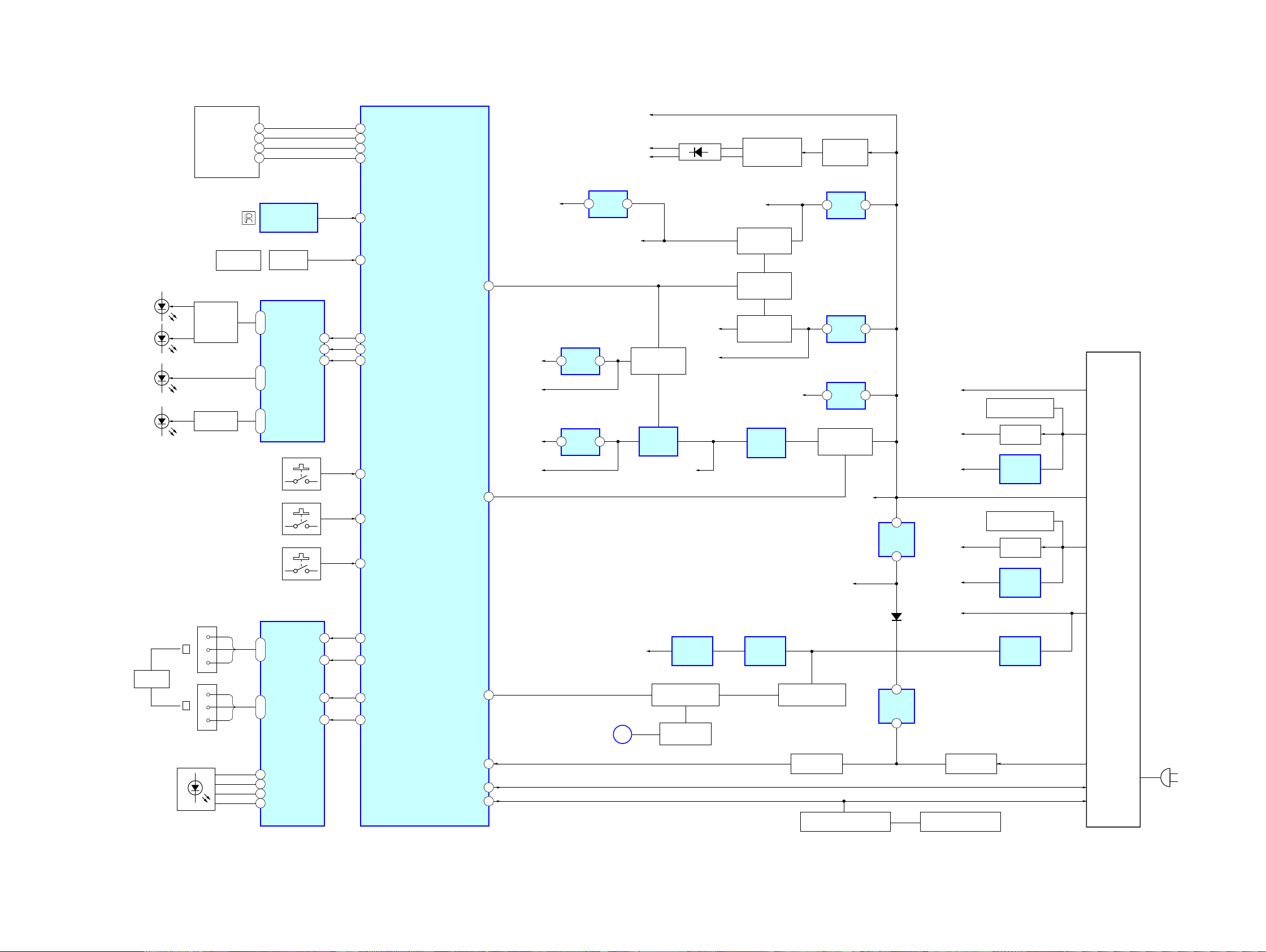
HCD-SHAKE7
6-4. BLOCK DIAGRAM - PANEL, POWER SUPPLY Section -
D1901, D1903,
D1902, D1904,
D2103 - D2106
D2601 - D2605,
D2614
D1905
D1906
VACUUM
FLUORESCENT
DISPLAY
ND2401
VOLUME /
DJ CONTROL
LED DRIVER
Q2604 - Q2612
LED DRIVER
Q2601 - Q2603
35
SI
36
CLK
37
LAT
38
BK
REMOTE CONTROL
5 - 13
14 - 17
18 - 20
S2201 - S2202
RECEIVER
ROTARY
ENCODER
LED DRIVE
OUT0
I
OUT8
OUT9
I
OUT12
OUT13
I
OUT15
IC2201
S2601
IC2601
TRANS
PWMCLK
SIN
LED +13.5V
O-FL-SOUT
99
O-FL-CLK
100
O-FL-LATCH
98
O-FL-BK
26
+3.3V REG.
IC901
+3.3V REG.
IC5
+1.2V REG.
SYSTEM CONTROLLER
IC11 (4/4)
4 I-SIRCS
92
I-MASTER-VOLUME
O-MTK-POWER-CTRL
O-RGB-SOUT
2
4
21
3
O-RGB-TRANS-LED
23
O-RGB-PWM-CLK
22
I-AD-KEY2
89
79
+1.2V
+3.3V
+5V
+3.3V
+5V +9V
IC302
15
43
TD FL
TUBE
81
+3.3V
POWER CONTROL
PROTECTION
+5V REG.
Q8, Q14
IC10
D2401 - D2404
+5.2V
+5.2V
DC-DC CONVERTER
TRANSFORMER
T2401
+3.3V
POWER CONTROL
PROTECTION
Q4
POWER CONTROL
PROTECTION
Q5
POWER CONTROL
PROTECTION
Q2
+9V REG.
IC4
+5V
SWITCHING
TRANSISTOR
Q2403, Q2404
+3.3V REG.
IC8
+5.2V REG.
IC6
+5V REG.
IC7
POWER CONTROL
PROTECTION
Q1, Q12
23
23
REGULATOR,
SWITCHING
(SMG-1800)
23
+VH
+18.5V
+5V
PROTECTION SWITCH
Q1050
+18.5V REG.
Q1027
+5V REG.
IC1006
+VH
+VL
LED
SPEAKER
CN4
2
R
3
4
CN2
2
L
3
4
D2101, D2102,
D2201, D2202
S2001 - S2011
S2101 - S2113
10 - 12
/OUT10
13 - 15
5
6
8
9
LED SELECTOR
IC14
/OUT5
I
/OUT7
PWMCLK
/OUT8
I
TRANS
/OUT0
/OUT1
/OUT3
/OUT4
SIN
SCK
+4V
Q18
+13.5V
5
+4V REG.
IC1
4
2
RESET IC
IC2
1
-18.5V
D1
-VH
AC-DET SWITCH
POWER CONTROL SWITCH
+13.5V
PROTECTION SWITCH
Q1051
-18.5V REG.
Q1029
-5V
Q17
Q3
-5V REG.
IC1007
-12.6V REG.
IC1014
-VL
-VH
AD-DET
V-CON
P-CON
(AC IN)
I-RESET
19
-44V
74
AMP SECTION
(Page 25)
10
77
78
C
-44.5V REG.
IC1016
PROTECTION SWITCH
Q1016
RESET SWITCH
Q1046, Q1049
-25.4V REG.
IC1015
PROTECTION SWITCH
Q1000
RESET SWITCH
Q16
LED POWER CONTROL SWITCH
O-PCONT-PSAVE-PROTECT
I-AD-KEY1
90
I-AD-KEY0
65
O-RGB-SOUT
2
3
21
4
3
O-RGB-SCLK
5
O-RGB-PWM-CLK
22
O-RGB-TRANS-LED-SPK
80
/I-SD-FAST
O-PCONT-7V-13.5V
O-PCONT-DAMP
HCD-SHAKE7
2626
Page 27
HCD-SHAKE7
Ver. 1.2
• Note for Printed Wiring Boards and Schematic Diagrams
Note on Printed Wiring Board:
• X : parts extracted from the component side.
• : parts extracted from the conductor side.
•
(The other layer’s patterns are not indicated.)
t Indication of transistor
• Abbreviation
AR : Argentina model
E2 : 120 V AC area in E model
E4 : African model
E51 : Chilean and Peruvian models
EA : Saudi Arabia model
MX : Mexican model
MY : Malaysia model
SAF : South African model
: Pattern from the side which enables seeing.
Caution:
Pattern face side:
(Conductor Side)
Parts face side:
(Component Side)
C
Q
B
D
Q
G
B
B
E
S
Q
CE
These are omitted.
These are omitted.
Q
CE
Parts on the pattern face side seen from
the pattern face are indicated.
Parts on the parts face side seen from
the parts face are indicated.
These are omitted.
These are omitted.
Note on Schematic Diagram:
• All capacitors are in μF unless otherwise noted. (p: pF)
50 WV or less are not indicated except for electrolytics
and tantalums.
• All resistors are in and 1/4 W or less unless otherwise
specifi ed.
•
2
• C : panel designation.
• A : B+ Line.
• B : B– Line.
• Voltage and waveforms are dc with respect to ground
under no-signal (detuned) conditions.
no mark : TUNER
< > : CD PLAY
* : Impossible to measure
• Voltages are taken with a VOM (Input impedance 10 MΩ).
Voltage variations may be noted due to normal production
tolerances.
• Waveforms are taken with a oscilloscope.
Voltage variations may be noted due to normal production
tolerances.
• Circled numbers refer to waveforms.
• Signal path.
F : AUDIO
f : TUNER (FM/AM)
N : MIC
J : CD PLAY
E : USB
• Abbreviation
AR : Argentina
E2 : 120 V AC area in E model
E4 : African model
E51 : Chilean and Peruvian models
EA : Saudi Arabia model
MX : Mexican model
MY : Malaysia model
SAF : South African model
: nonfl ammable resistor.
Note: The components identifi ed by mark 0 or
dotted line with mark 0 are critical for safety.
Replace only with part number specifi ed.
model
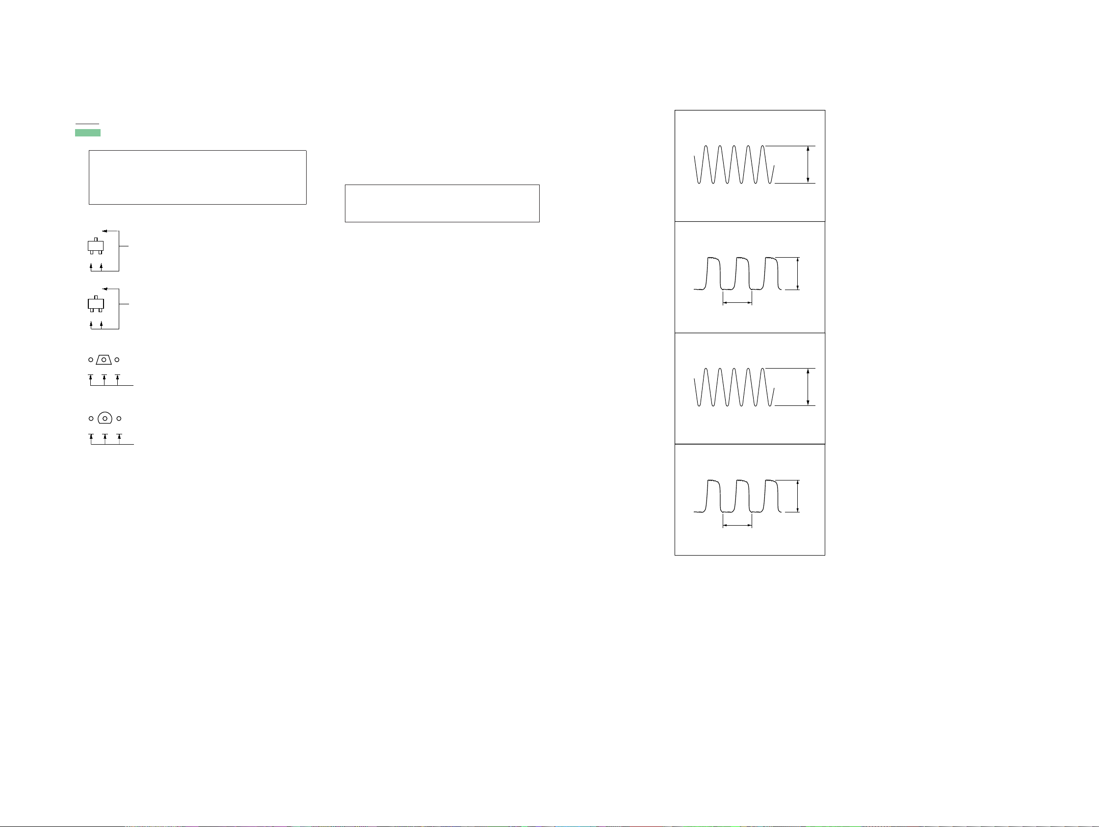
• Waveforms
– MOTHERBOARD Board –
1 IC9 es (XTAL2)
24.0 MHz
20 mV/DIV, 10 ns/DIV
120 mVp-p
2 IC11 8 (I-X-CIN)
75.2 mVp-p
32.76 MHz
20 mV/DIV, 10 Ps/DIV
3 IC11 qd (I-Xin)
8.0 MHz
50 mV/DIV, 50 ns/DIV
236 mVp-p
4 IC656 4 (XTALO)
198 mVp-p
12.28 MHz
50 mV/DIV, 25 ns/DIV
HCD-SHAKE7
2727
Page 28
HCD-SHAKE7
Ver. 1.1
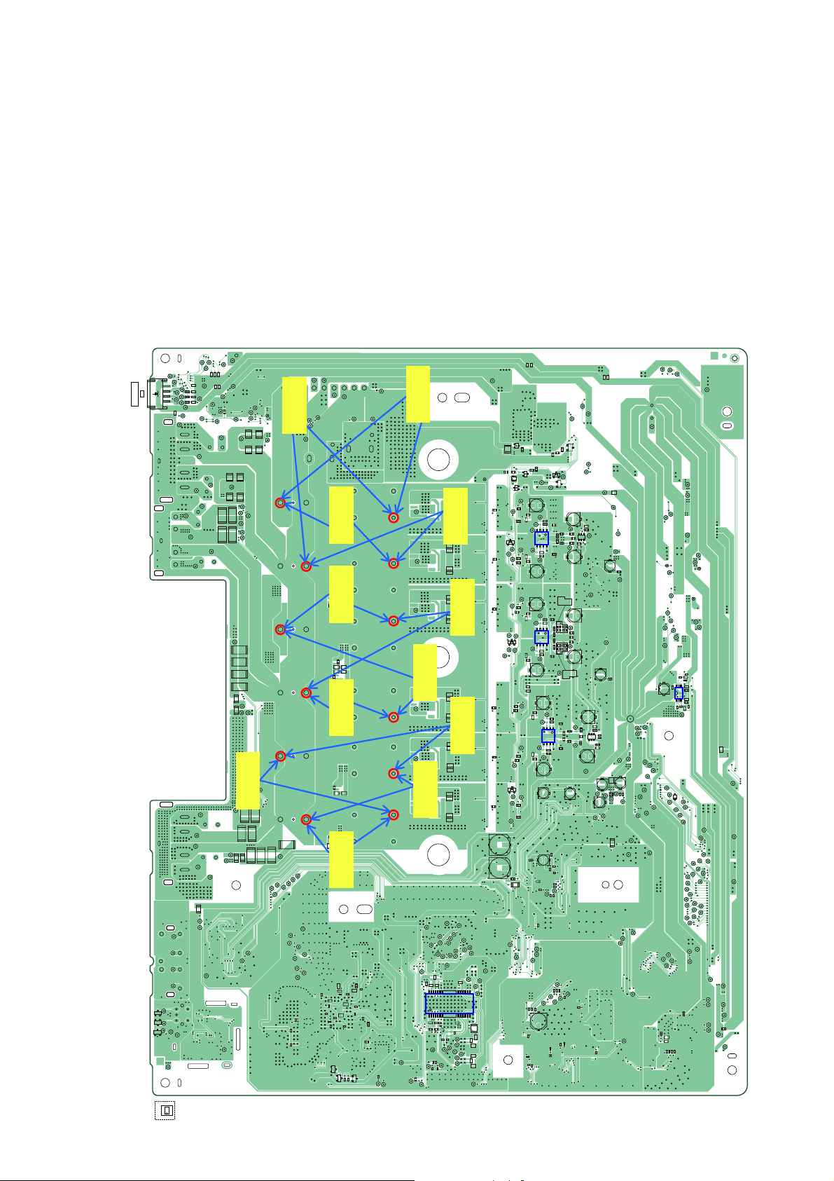
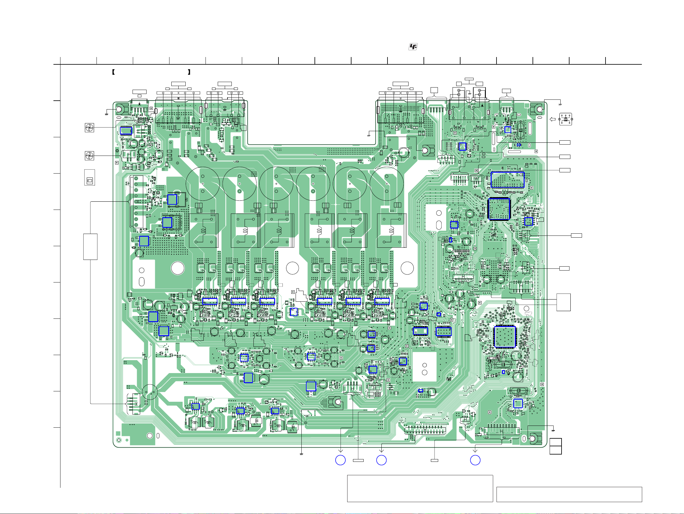
6-5. PRINTED WIRING BOARD - MOTHERBOARD Board (Component Side) - • See page 22 for Circuit Boards Location. • : Uses unleaded solder.
1
A
B
DC FAN
DC FAN
C
Q1010, Q1011,
Q1012, Q1013,
Q1014, Q1015,
Q1016
B2E2C1
B1C2E1
D
E
CONNECT TO
SWITCHING
REGULATOR
(SMG-1800)
BOARD
F
G
H
I
J
K
2 3 4 5 6 7 8 9 10 11 12 13 14 15 16
MOTHERBOARD BOARD (COMPONENT SIDE)
(CHASSIS)
LP1
13 24
R81
R97
R121
TB1002
SUBWOOFERS
R1138
D1005
R1097
D1014
R1051
D1015
D1004
R1216
C1324
IC1006
KA
+–
C1200
D1010
Q1016
R1217
C1366
E
C1327
Q1000
D1057
C1103
I
IC1007
R1180
Q1022
,03('$1&(86(
(CHASSIS)
C1348
C1277
C1020
C1060
R1472 R1473
R1045
R1412
C1168
JL1090
C1171
IC1014
OI
A1002
IC1015
OI
D1058
D1041
AK
AK
D1016
R1093
C1229
D1020
C1230
Q1029
E
R1094
D1017
D1019
R1139
O
C1044
R181
R120
Q6
R41
R1144
+– + –+ – + – + –
C1351
C1061
C1021
C1278
C1349
R1041
JL1106
A1001
C1138
C1360
L1007
KKA A
D1042
D1027
R1454
R1311
R1302
R1013
KA
Q1027
E
D1026
C1194
C1212
R1205
R1204
C1195
R1348
C1234
C1328
R1272
R1278
C1095
R1322
Q1019
C92
R156
C11
IC6
C159
JL140
L8
R49
C10
R46
C78
C1
CN2
LED
SPEAKER
L
ET5
IC14
C105
C1045
Q1050
14
C114
C208
R16
R15
C215
R12
C110
R13
R14
R147
R11
C209
C106
R17
112
C109
R57
CN1001
12
R1115
C1315
Q1046
D1018
R1428
E
Q3
R110
R1419
R1418
Q18
R1048
R1047
12
CN1000
R1046
R1159
Q1057
C1042
C1210
C108
C1317
C1041
R1415
C1209
R1268
R1083
C1316
Q1032
R1117
Q1030
Q1058
E
E
R1050
R1057
R1215
D1007
R1212
R1175
R1154
R1155
CN1002
R1213
R1174
R1142
R1141
C1326
C1325
19
D1056
K
A
K
A
D1055
D1023
C1231
IC1016
OI
C1089
C1107
C1232
R1430
C1102
R1103
C1233
OI
C1043
R1125
R6
C85
15
C212
CN1
C9
C1350
R1474
C1169
C1170
C1158
Q1039
R1239
R1071
AK
C1111
R1024
E
R1156
C1121
C1120
R1105
R1386
R197
R198
C73
C56
C1023
IC1002
Q1011
C160
C203
C222
TB1001
MID SPEAKERS
,03('$1&(86(
(CHASSIS)
C1353
C1178
C1279
C1352
E
E
Q1004
Q1052
C1062
R1198
E
Q1005
C1177
R1200
Q1055
E
R1220
R1043
C1164
C1165
Q1044
R1284
R1030
R1455
R1240
R1252
R1072
D1031
TH1000
AK AK
C1153
R1312
KA
R1012
D1035
R1003
R1111
C1213
R1025
C1329
C1304
C1228
C1211
R1151
R1349
R1347
R1133
C1037
C1203
C1330
R1277
R1269
C1098
Q1020
R1287
R1293
R1294
R1288
Q12
R38
R39
E
Q1
R140
R201
R35
R146
Q2
E
JL143
L14
TB1000
TWEETERS/WOOFERS
,03('$1&(86(
LRLRL
C1354
C1025
C1282
C1355
C1064
R1475
R1040
R1223
R1410
C1156
C1136
C1361
L1010
C1159
C1137
C1362
L1009 L1012
C1157
C1141
C1363
R1411
C1140
L1008
(CHASSIS)
R1147
R1203
C1160
C1022
R1044
JL1092
R1476
Q1047
JL1058
R1173
R1195
Q1021
C1161
L1011
R
(CHASSIS)
C1281
C1065
C1356
C1358
C1280
C1357
C1063
C1101
JL1061
JL1095
R1202
R1214
R1146
R1409
C1139
CN3
FOR
(factory
SERVICE
internal
USE
use only)
15
C1024
C1359
R1042
R1477
R781
R780
R778
R776
ET1000
2918
CN11
C343
IC302
C927
R905
C913
FB902
R917
Q1034
Q1037
Q1040
Q1043
R748
IC660
R1247
R1068
C1331
C1223
R736
R734
C164
L10
R1283
R1033
D1028
TH1004
R1010
D1025
R1001
R1018
C1214
R1350
R724
R728
C734
R746
R742
C658
C732
R726
R722
IC4
OI
C204
R43
R45
R185
R141
C57
C75
L13
R1458
R1313
R1303
R1015
R1242
C1112
KA
R1026
C1215
E
R1157
R1351
C1332
R1279
R1273
C1096
R1318
Q1023
R731
R754
C779
C713
C789
C711
R732
C781
R756
R7
JL153
R1285
R1031
R1073
R1241
R1459
R1074
TH1002
R1014
C1154
R1314
IC1001
R1004
R1107
C1333
C1300
C1225
R1352
R1132
Q1010
C1039
C1202
C1123
C1122
R1099
R1387
C773
C800
R667
C771
R665
C801
R5
C83
Q4
R148
Q5
E
R109
R191
C16
IC8
C162
L12
R51
C17
R48
C3
C80
C1094
R1420
C1298
L1000
Q1025
C1305
R1095
R1143
R1027
C1216
C1034
C1201
R1289
JL1004
C747
R1291
JL1001
C750
C165
R199
C205
R200
C58
C77
C223
L15
R1456
R1309
R1300
R1008
R1066
R1457
C1152
C1110
R1305
R1023
IC1004
R1110
C1303
E
R1136
Q1014
C1204
C1036
C1114
C1118
R1101
R1321
R1383
C751
JL1008
C656
JL1006
C752
R738
C12
R153
C14
IC7
C161
R50
C15
R47
C79
C2
C1334
R1276
R1271
R1319
(CHASSIS)
C1115
C1117
R1385
IC1008
R1253
D1030
AK
AK
R1100
D1034
C1218
R1353
R1150
R735
C733
R747
C655
IC658
C731
R737
R733
IC10
OI
R142
R143
JL159
MIC BOARD
NO2301
Q1035
R1460
R1308
R1301
R1006
R1065
R1461
C1108
R1307
R1021
IC1003
R1109
E
R1137
Q1015
R727
R723
R745
C712
C657
R741
C710
R725
R721
C780
C13
C166
(Page 48)
Q1041
Q1036
R1462
R1316
R1281
R1304
R1034
R1017
R1244
R1075
R1246
R1070
C1151
R1011
C1335
R1020
C1302
C1224
C1208
R753
C778
C761
R729
C788
R730
C763
R755
Q8
E
R4
R1463
D1029
TH1003
AK
C1113
R1315
AK
D1024
R1028
IC1000
R1002
R1106
C1219
E
C1217
R1158
R1355
R1354
R1134
Q1012
C1038
C1035
C1207
C1336
R1280
C1097
R1274
R1317
Q1024
R666
C772
R664
C770
R145
R36
Q14
CN9
ET1
A
Q1042
C1155
C1299
C1124C1125
R1098
R1388
14
BLUETOOTH
Q1033
Q1038
R1464
R1310
R1286
R1299
R1032
R1007
R1235
R1243
R1076
D1032
TH1001
AK
C1109
R1016
AK
D1033
R1022
R1005
C1221
C1337
R1029
C1226
E
C1220
R1149
R1357
R1356
C797
IC651
C741
C798
C742
IC652
R176
R161
C40
C139
R122
C41
IC13
R123
C88
JL185
C51
JL183
CN10
R223
R225
R227
R229
R1282
R1035
R1245
R1067
R1465
R1069
TH1005
R1009
C1150
R1306
C1338
R1275
IC1005
R1108
R1135
Q1013
R685
R686
R687
R688
R689
R690
C53
C54
R162
C137
R174
R159
C52
R222
R226
R228
R224
C1116
R1000
R1270
C1093
C687
C1119
R1102
C1301
C686
R1320
R1384
Q1026
C1339
R1019
C1222
C1227
R1358
C766
C737
C783
R822
R821
R707
R823
R695
C685
R712
R829
C717
C675 C676
R675
C682
IC654
R711
C796
C795
C743
C674
C726
R2
2
1
C213
C214
R709
R708
R830
C716
C684
R160
R676
R674
R825
R827
R826
R720
IC655
R719
C677
C744
C678
C794
R717
JL656
C802
C739
C714
C670
38 20
C671
IC656
119
C669
R813
JL653
R749
X651
C767
R713
JL651
R694
R693
C18
IC1
C20
C19
C45
CN12
R698
R710
C660
C679
C727
R704
R699
R714
JL652
BUTTON_R
BOARD
B
CN2002
(Page 47)
FB301
R652
C785
C667
C804
R692
R696
R673
R691
C673
R697
R718
IC664
R706
R703
R702
R701
R700
R680
R681D5R682
C715
R818
14
IC653
R819
C672
R716
R683D7R684
R705
R831
R832
R715
D1
C101
24
25
NFC
J651
AUDIO IN
PC/
GAME
L
R
(CHASSIS)
C662
R662
R678
R663
R740
C654
C661
C704
C706
R810
R809
R808
R807
IC661
R787
C701
C699
CN307
16
CL317
CL315
CL318
CL319
R343
R332
C368
C367
IC901
R348
R344
C928
C926
CL913
R930
R932
R921
R929
R931
R933
R928
C925
CL910
CL914
Q901
R902
EE
R924
R923
R901
C902
R336
R340
R341
R342
R379
1
CN305
2
C328
C329
C327
R303
R651
C784
C803
R670
R669
C681
R672
R668
R671
C680
R679
1
JL71
JL253
2815
JL254
R37
Q15
2178
CN8
TV/DVD/
SAT
L
R
C652
R656
R659
R661
R657
C651
C653
C705
C659
R786
R782
R779
R785
R784
R777
R775
R783
R788
C700
C698
Q652
CN308
RB308
RB305
1
3
RB309
R385
CL311
CL314
CL313
R381
CL312
97
JL310
C312
CL316
CL320
R307
R308
CL321
CL322
C356
R310
CL323
128
R309
C366
R334
CL302
R314
CL301
R333
R922
Q902
C345
JL256
SL908
C904
SL907
R920
R918
CL908
23
24
CL907
CL906
C346
C347
R304
C363
JL1009
JL62
R88
R89
R90
JL67
R91
JL68
R92
R22
R94
R95
JL246
R96
R40
JL255
R129
R108
R113
R105
C7
R114
JL77
JL79
R115
JL3
R104
R55
JL5
R20
C42
R178
R116
Q9
R149
E
C34
C30
USB
BOARD
C
NO2201
CN7
ANTENNA
FM/AM
13
R102
C142
L2
C59
C141
L1
L3
L5
R213
R151
C67
R103
C702
R384
C924
JL2
IC3
C163
C61
C50
R52
C207
R364
C341
C320
IC304
RB307
RB306
CL310
96
IC306
132
R382
X301
C362
C358
CL901
CL902
CL903
CL909
C923
R107
JL59
JL60
R84
JL251
R87
R85
JL61
JL63
R128
R138
JL64
JL58
R137
JL65
JL57
JL66
75
JL69
76
JL245
C8
JL78
100
1
JL1
JL4
JL8
R194
C130
R111
JL6
X1
X4
JL7
R180
C132
C43
D8
Q16
JL247
CN6
C27
R53
C69
C70
R214
L6
R190
C71
R221
C318
C319
RB304
RB303
R306
R325
65
64
R338
C333
R316
33
R371
R370
R369
JL309
JL308
CL912
D901
D902
SL905
SL906
CL904
R926
CL905
R925
16
R77
R78
R76
JL56
R83
JL53
JL51
JL48
R82
R135
R75
JL50
JL52
R134
JL49
JL46
C5
JL55
JL54
51
50
IC11
26
25
R182
JL9
C4
JL10
R184
C103
C102
JL12
JL192
C93
1
R117
IC2
X2
C129
C35
1
C36
9
R212
C38
R211
R210
R209
110
C26
IC5
CL306
R311
R315
R903
CN901
R230
JL47
JL45
C81
JL13
R203
36 28
10 18
C97
C37
X3
1
C317
RB302
R375
CL308
JL301
CL307
R312
CL305
R355
IC305
R327
CL911
C911
C912
R904
JL249
R70
R71
JL40
JL44
JL39
JL250
JL38
JL36
JL35
JL33
JL32
JL30
JL27
JL25
JL22
JL18
JL17
Q17
R150
C55
C131
27
IC9
19
1-887-113-
ET2
C119
C62
C63
C68
R330
R329
R331
C350
127
RB301
5428
R361
R339
R377
JL302
R323
R322
R321
R354
R320
CL304
CL303
C314
13
CN301
51
42
R346
CN306
R345
R66
JL42
JL41
JL43
R67
R31
R126
JL37
R64
R65
R68
JL31
JL29
R69
JL28
R63
R62
JL26
R193
R61
JL24
JL23
R216
R192
JL21
R215
R79
JL20
JL19
R34
R21
R54
JL14
JL15
JL16
R164
JL248
R86
R58
R59
C60
R112
C206
JL167
JL166
R186
R183
C31
R100
C33
C95
C39
C32
R101
R168
C29
C96
ET6
(CHASSIS)
S1
123
L3
64
S2
FLASH
PROGRAMMING
FLASH
PROGRAMMING
FLASH
PROGRAMMING
JL303
JL305
R318
R317
JL306
JL307
R319
R376
FLASH
PROGRAMMING
CONNECT TO
MS-476
SERVICE,
OPTICAL
DEVICE
(CHASSIS)
21
(21)
(Page 49)
HCD-SHAKE7
Note 1: IC304, IC305 and IC306 on the MOTHERBOARD
board cannot exchange with single. When these
parts on the MOTHERBOARD board are damaged,
2828
exchange the entire mounted board.
Note 2: When the MS-476 board is defective, exchange the
entire LOADING ASSY (T).
Page 29

6-6. PRINTED WIRING BOARD - MOTHERBOARD Board (Conductor Side) - • See page 22 for Circuit Boards Location. • : Uses unleaded solder.
HCD-SHAKE7
1
A
B
C
D
E
F
G
H
I
J
K
2 3 4 5 6 7 8 9 10 11 12 13 14 15 16
MOTHERBOARD BOARD (CONDUCTOR SIDE)
D2
D3
Q1009, Q1045
B2E2C1
B1C2E1
JL280
D305
R353
R352
D300
CL324
R368
CL325
CL326
R378
CL333
C305
C304
JL314
JL304
JL197
CL2
JL285
C322
D306
R383
CL334
JL316
JL315
R350
R349
JL312
JL313
JL903
JL905
JL906
JL902
JL904
C907
C908
SL902
SL903
SL904
C133
C135
C134
JL34
R125
R132
R165
R130
JL11
R167
R171
C28
R172
R173
JL89
JL284
D4
JL196
JL195
JL194
C321
R363
C337
C334
C336
C338
C335
C332
C352
C309
C331
R324
C920
R919
1
C922
R908
78
C302
R906
29
C303
C326
JL901
C915
14
R927
SL901
R133
R127
R136
R154
C82
JL73
JL74
R166
C144
R44
C94
R32
JL95JL96
JL91
JL94
R33
JL98
C351
R366
JL190
C364
IC902
JL340
JL90
JL657
JL658
C311
C365
C339
C313
C348
C308
2815
30
JL70
JL72
R72
R139
JL76
JL665
JL664
R217
JL88
JL225
JL674
CL336
CL337
CL309
C349
R305
JL335
R916
C921
C919
JL330
C918
JL334
22
JL336
JL332
JL327
21
C916
JL338
JL339
JL341
JL227
JL252
R155
JL75
JL120
JL123
JL117
JL106
JL97
JL80
JL671
CL329
CL327
CL332
CL328
CL331
CL330
JL329
JL326
JL322
JL318
JL328
JL324
JL320
JL319
JL325
JL321
JL331
JL323
JL337
JL333
JL661
JL175
JL169
R817
JL178
JL191
JL102
JL161
JL121
JL118
JL119
JL133
JL273
JL193
JL277
JL272
JL271
JL1064
JL1069
JL1075
JL1071
JL1149
JL1105
C1172
C1173
JL87
JL85
JL86
JL84
JL83
JL82
JL81
R824
R828
C728
R816
JL654
R812
R750
C768
C769
R751
R814
JL655
JL110
JL112
JL114
JL113
JL109
JL111
JL115
JL99
JL108
JL116
JL122
JL107
JL170
JL1068
JL1065
JL1102
R1360
R1373
R1381
R1369
R1364
JL1117
R1366
C1377
R1452
C1378
C792
C799
R653
C740
C683
C668
R820
JL663
JL660
JL226
JL100
JL101
JL163
JL104
JL212
JL105
JL164
C1166
JL1114
JL1112
R1382
JL1113
JL1057
R1361
C1167
JL1054
R1449
C1375
C1376
JL1098
C1051
C1048
R1171
JL1124
JL1088
JL1126
R1131
R1055
JL1085
C806
JL188
JL103
C90
JL124
JL189
JL186
R175
JL184
C138
JL278
JL126
JL162
JL213
JL125
JL132
JL134
JL130
KA
JL128
JL279
D9
JL257
JL129
JL1101
C1058
C1059
R1179
D1001
JL1082
R1053
R1127
JL1077
C1032
R1082
JL1046
C805
JL187
JL1048
C1199
R1194
C1246
R1163
JL1033
JL1139
C89
R177
C140
C91
JL127
JL131
JL165
R1230
C1189
C1323
JL147
JL92
JL172
JL662
JL93
R1
C1174
C1175
R1372
JL1103
JL1107
JL1094
R1446
JL1096
C1050
C1046
R1172
R1130
R1054
C1346
C1347
JL1083
C1031
R1080
JL1043
IC1012
JL1039
C1206
C1243
R1192
R1207
R1209
R1160
R1090
R1092
JL1032
R1266
R1226
C1184
R1423
C1322
Q1009
R1424
R1295
R1296
JL136
JL173 JL174
JL224
R99
JL282
R158
C25
R106
JL1142
C1319
C745
R654
C87
C23
IC12
R98
C22
C21
R157
C24
R195
R196
JL1116
R1370
R1363
R1368
C1373
C1371
R1443
C1374
C1372
JL1143
D1000
JL1121
JL1089
C1033
R1081
JL1045
JL1049
R1193
C1245
C1205
R1404
R1467
R1162
R1470
R1471
C1380
R1091
C1188
JL1034
R1231
JL1002
JL659
R219
C1369
C1370
JL1100
C1057
R1178
JL1080
JL1010
R1052
JL1122
C1030
R1079
JL1044
IC1011
JL1040
R1191
C1242
R1466
R1406
R1161
C1185
JL1031
R1227
R1265
JL179
JL181
JL180
JL155
JL156
JL157
JL160
JL1070
JL1074
R1440
JL1097
C1056
JL1079
R1128
C1198
C1318
R1468
C1379R1469
R1089
JL1003
JL146
JL177
JL158
C1047
C1049
R1170
JL1123
JL1087
R1129
R1056
JL1084
R1078
JL1042
C1307
R1211
C1197
JL1047
R1119
C1182
JL1007
C746
JL148
R655
JL149
JL150
JL152
JL151
JL154
JL1066
JL1072
JL1093
R1362
R1380
R1359
JL1110
JL1055
R1437
C1367
C1368
D1002
JL1125
JL1128
JL1041
IC1010
C1244
R1210
R1183
R1184
R1118
R1088
R1087
JL1030
JL1035
R1264
R1225
R1234
Q1045
C1321
R1421
JL237
R1422
C1320
JL145
JL176
R1367
R1379
R1365
JL1115
JL1073
JL1104
JL1111
JL1099
C1054
C1055
R1177
JL1081
Q1048
JL1078
R1058
R1126
C1306
R1077
JL1038
C1196
JL1127
JL1129
C1241
D1006
C1192
JL1011
JL1136
R3
JL144
JL142
JL141
JL1067
JL1091
R1371
JL1118
R1374
JL1120
R1145
Q1017
R1084
Q1049
R1181
R1182
D1003
JL1130
JL168
JL182
JL139
JL1131
JL1109
JL1119
R1376
R1375
R1377
R1378
JL1108
JL1147
JL1036
JL1146
R1431
Q1051
R1433
R1434
R1401
R1402
E
Q1007
JL135
CN4
LED
SPEAKER
R
JL281
JL199
C221
JL201
JL200
JL206
JL205
JL207
JL198
JL238
R27
R24
R25
C116
JL1132
JL241
JL1135
JL1062
JL1063
R1435
JL1145
JL1012
JL1050
JL1148
JL1020
JL1014
JL1086
JL1037
JL1017
JL1018
JL1133
JL1137
JL1022
JL1021
JL208
C118
C117
C115
JL209
JL215
JL204
C99
C219
C98
C100
C220
JL262
JL276
JL214
JL1015
JL1016
JL1076
JL1019
C217
C218
C210
C211
JL138
JL275
JL137
JL283
21
1-887-113-
(21)
HCD-SHAKE7
Note: IC902 on the MOTHERBOARD board cannot exchange
with single. When this part on the MOTHERBOARD board
is damaged, exchange the entire mounted board.
2929
Page 30

HCD-SHAKE7
6-7. SCHEMATIC DIAGRAM - MOTHERBOARD Board (1/10) - • See page 27 for Waveforms. • See page 53 for IC Block Diagrams.
1
A
MOTHERBOARD
BOARD
(8/10)
(Page 37)
B
C
D
E
MOTHERBOARD BOARD
F
G
H
(9/10)
(Page 38)
MOTHERBOARD
BOARD
(8/10)
(Page 37)
AUDIO IN
PC/GAME
R
L
J651
4P
RL
AUDIO IN
TV/DVD/SAT
JL658
JL665
C662
I
J
MOTHERBOARD
BOARD
(10/10)
(Page 39)
K
JL657
JL664
0.1
4
R656
C652
39k
220p
2 3 4 5 6 7 8 9 10 11 12 13 14 15 16 17
MOTHERBOARD BOARD (1/10)
TAS-RESET
TAS-INT
TAS-MUTE
TAS-IIC-DATA
1
TAS-IIC-CLK
3
ANALOG-BSEL
ANALOG-ASEL
2
BT-R
TUNER-L
TUNER-R
IC B/D
IC653
ASYNCHRONOUS
SAMPLE RATE
CONVERTER
BT-L
4.7C699
4.7C698
R817 0
R679 10
R680 10
R681 10
R682 10
C715
0.01
R818
0
1.5
1.1
1.4
1.4
3.3
3.1
0
1
LGAP
2
RCKI
3
NC
4
SDIN
5
BCKI
6
LRCKI
7
VIO
8
DGND
9
BYPAS
10
IFMT0
11
IFMT1
12
IFMT2
13
RST
14
MUTE RDY
R819 0
IC653
SRC4182
MODE2
MODE1
MODE0
BCKO
LRCKO
SDOUT
DGND
TDMI
OFMT0
OFMT1
OWL0
OWL1
28
27
26
1.4
R683 10
25
1.4
R684 10
24
1
R705 22
23
3.3
22
VDD
C672
21
20
19
18
17
16
15
0.1
3.3
0
R749 10k
R713 100
C669 0.1
R714 100
R715 100
R716 100
1.5kR832
1.5kR831
10kR750
10kR751
12.288MHz
1
X651
C768
R812
0
10pC767
0.1C668
10pC766
1.7
2
1
R813 0
0.6
R814 0
JL651
0
3.3
1.2
1.2
C769
10p
10p
JL652
0
JL653
2
2.1
JL654
2.6
JL655
2.6
1.4
R699
22
4
1
2
3
4
5
6
7
8
9
10
11
12
13
14
15
16
17
18
19
C671 0.1
AVSS
VR_PLL
XTALI
XTALO
MCLKI
MCRCK_DV
CS0
RESET
GPIO
DVDD
DVSS
SDIN1
VR_DIG
SDIN2
SDOUT1
SDIN3
SDOUT2
SDIN4
SDOUT3
SDA1
SDOUT4
SCL1
SCLKOUT2
SDA2
SCLKOUT1
SCL2
MCLKO
LRCK
SCLKIN
IC656
TAS3108DCPR
10 16VC740
AVDD
RSRV
PLL2
PLL1
PLL0
RSRV
PDN
DVDD
DVSS
39
38
37
36
35
34
33
32
31
30
29
28
27
26
25
24
23
22
21
20
IC B/D
IC661
R661
R662
R740
39k
39k
39k
MIC_IN
SELECTOR
R657
10k
R659
10k
R663
10k
R678
10k
Q652
RN1902
ANALOG
C651
100p
C654
100p
C661
100p
C653
100p
R
L
R
L
PCM1808PWR
R829
1k
IC654
IC B/D
IC654
STEREO A/D
CONVERTER
R708
22
R709
22
C684
C685
SIGNAL SELECTOR
JL671
Q652
0
0
5
3.1
JL674
1.4
10R695
1
22R707
0
0R821
0
0R822
0
0R823
2.4
2.4
R711
4.7
47
R712
47
4.7
GND
B
10
9
R788
47k
C659 0.1
C702
C706
8
LRCK
BCK
9
SCKI
DOUT
10
DGND
MD0
11
MD1
12
FMT
13
AGND
VINL
14 VREF
VINR
0.01C716
0.01C717
1kR830
4.7C705
4.7C704
2.5
2.4 2.5 2.4 2.5
Y3
Y1
INH
GND
IC661
SN74LV4052APWR
A
X312X013X14X115X216VCC
11
5
R787
47k
4.7
4.7
1.5
7
1.4
6
5
C676
3.3
0.1
4
VDD
VCC
C796
5
0.01
3
C675
0.1
2
2.4
1
C743
10 16V
IC655
PCM1808PWR
IC B/D
R808 47k
R807 47k
R784 47k
R783 47k
0.1C795
47kR810
47kR809
47kR786
47kR785
12345678
Y
Y0
Y2
2.42.42.4 2.52.4 50
10R694
10R693
C726
10
R820
0
0.1C674
R778 47k
R776
R777 47k
R775 47k
C687
4.7
C799
220
6.3V
47kR781
47kR780
47k
4.7C700
4.7C701
47kR782
47kR779
R720
100
C744
10
16V
C792
220
6.3V
AVDD5V
IC655
STEREO A/D
C686
CONVERTER
4.7
0R827
0R826
0R825
R719
100
2.4
2.4 3.3 1 1.4
14 13 12 11 10 9 8
FMT
VINL
VINR
AGND
VREF
VCC
C678
C794
0.1
0.01
C677
0.1
R824
22R828
22R710
MD0
MD1
DOUT
VDD
DGND
SCKI
54321
C679
C727
0.1
10
10R696
0
ACLK
10R698
LRCK BCK
76
1.51.43.352.4
0.1C660
10R697
ADIN
ALRCK
ABCK
ASDATA0
3.3
3.1
3.3
3.3
1.6
1.1
1.1
1.4
1.4
1.5
R691
R692
R706
10
10
22
JL656
R653
3.3
1.2
0
C739
10 16V
C714
0.01
4.7C728
C670
0.1
22R704
22R703
1kohmR702
22R701
22R700
0R816
IC664
TC7WH157FK
IC B/D
IC664
SIGNAL SELECTOR
A
1
B
2
_Y
3
GND5Y
4
VCC
C802
_ST
SEL
0.1
C784
C803
100
0.1
10V
C785
C804
100
0.1
R717
100
10V
IC B/D
8
7
6
IC656
AUDIO DSP
C805
10
16V
C806
10
16V
3.3
C673
R718
0
100
1.2
DMB-AGND
C783
100
10V
R685
C798
0.1
ASEL
C667
0.001
C737
0.1
PCM1754DBQR
1.4
10
1
BCK
1.1
10R686
2
DATA
1.4
10R687
3
LRCK
4
2.5
2.5
1.4
10R688
1.1
10R689
1.4
10R690
2.5
2.5
DGND
5
NC
5
6
VCC
7
VOUTL
8
VOUTR
1
BCK
2
DATA
3
LRCK
4
DGND
5
NC
5
6
VCC
7
VOUTL
8
VOUTR
IC652
PCM1754DBQR
R667
C797
0.1
0.1
0R651
R6700R6690R668
0
R673
R672
0
0
R652
0
R675
R676
00
0
IC651
SCK
16
FMT
15
MUTE
14
DEMP
13
TEST
12
ZEROA
11
VCOM
10
9
AGND
0R664
C770
100p
C772
100p
0R666
SCK
16
FMT
15
MUTE
14
DEMP
13
TEST
12
ZEROA
11
VCOM
10
9
AGND
0R665
C771
100p
C773
100p
0
R674
FE_3.3V_1
DVDD3.3V
JL659
C680
0.1
C681
R671
0.1
0
C682
0.1
1.5
C741
10
16V
2.5
1.5
IC B/D
IC651
STEREO D/A
CONVERTER
C763
4.7
50V
C761
4.7
50V
R730
R729
JL661
JL660
JL662
C683
0.1
JL663
R723
2.7k
R721
2.7k
C710
1000p
R737
47pC780
10kR753
10kR755
4.7k
C750
10 16V
3.3k
3.3k
47pC778
R733
R725
2.7k
C731
820p
3.9k
DGND
FE_5V
AVDD5V
DGND
DMB-DVDD+3.3V
DMB-DVDD+5V
DMB-AVDD+5V
DMB-AGND
AVDD9V
4.5
4.5
4.5
R654
22
5
+
6
-
7
OUT
9
8
VCC
C745
10 16V
IC B/D
IC652
STEREO D/A
CONVERTER
C742
10
16V
2.5
C801
4.7
R732
50V
3.3k
C800
4.7
R731
50V
3.3k
0.1C779
0.1C781
10kR754
10kR756
R724
2.7k
R722
2.7k
R726
4.5
C711
1000p
R738
4.7k
C752
10 16V
C732
820p
R734
3.9k
2.7k
R655
5
+
4.5
6
-
4.5
7
OUT
9
8
VCC
C746
22
10 16V
MOTHERBOARD BOARD (3/10)
5
(Page 32)
MOTHERBOARD BOARD
6
(2/10), (3/10)
(Page 31), (Page 32)
MOTHERBOARD BOARD (1/10)
7
(Page 30)
MOTHERBOARD BOARD
IC658
OP AMP
IC658
BA4558F
0.1C655
4.7kR741
IC660
OP AMP
IC660
BA4558F
0.1C656
4.7kR742
GND
OUT
GND
OUT
8
+
-
+
-
4
3
2
1
C788
47 6.3V
4
3
2
1
C789
47 6.3V
(Page 39)
R727
2.7k
4.5
4.5
R735
4.5
3.9k
4.7kR745
C747
0.1C657
10 16V
R728
2.7k
4.5
4.5
R736
4.5
3.9k
4.7kR746
C751
0.1C658
10 16V
(10/10)
C733
820p
C712
1000p
R747
4.7k
C734
820p
C713
1000p
R748
4.7k
FRONT-L
AGND
FRONT-R
SW-L
AGND
SW-R
9
MOTHER-
BOARD
BOARD
(4/10)
(Page 33)
HCD-SHAKE7
7
MOTHERBOARD BOARD (1/10)
(Page 30)
10
MOTHERBOARD BOARD (2/10)
(Page 31)
3030
11
MOTHERBOARD BOARD (8/10)
(Page 37)
Page 31

6-8. SCHEMATIC DIAGRAM - MOTHERBOARD Board (2/10) - • See page 53 for IC Block Diagrams. • See page 62 for IC Pin Function Descriptions.
HCD-SHAKE7
Ver. 1.1
MOTHERBOARD
A
B
(Page 30), (Page 32)
C
D
E
F
MOTHERBOARD
G
H
MOTHERBOARD
I
J
K
HCD-SHAKE7
1
BOARD
(3/10)
(Page 32)
MOTHERBOARD
BOARD
(1/10), (3/10)
SERVICE,
OPTICAL
DEVICE
(1/2)
MOTHERBOARD
BOARD
(3/10)
(Page 32)
BOARD
(3/10)
(Page 32)
MOTHERBOARD
BOARD
(9/10)
(Page 38)
BOARD
(3/10)
(Page 32)
FLASH
PROGRAMMING
MOTHERBOARD
BOARD
(2/10)
(Page 31)
2 3 4 5 6 7 8 9 10 11 12 13 14 15 16 17
MOTHERBOARD BOARD (1/10)
(Page 30)
10
GND
C313 0.1
AGND12
AVDD12_1
NC
3.3 0 3 0 03.3 3.3 2.50 3.31.2 3 3.3 1.1 0.83.3 1.4 2 1.5 1.2 1.2 1.1 1.1 2.6 1.1 1.1 1.1
CL305
100R338
R321 10k
JL304
JL305
IFSDI
XSYSRST
C339 0.01
IFSDI
R322 0
JL303
C365 1
ADACVDD1
ADACVDD2
IFCS#
IFBSY
R323 0
JL302
XIFCS
XIFBSY
CL323
CL306
1kR311
JL301
ASDATA0
100R310
ASDATA0
MFISW
CL307
3.3kR354
MFISW
ALRCK
ABCK
ACLK
CL318
CL319
CL322
100R309
1kohmR308
100R307
C349 10
CL321
CL320
NC
NC
ACLK
ABCK
AVCM
ALRCK
FOCUS/TRACKING ERROR AMP
CD SYSTEM PROCESSOR
DIGITAL SERVO PROCESSOR
MUTE
LIMITSW
46 47 48 495051 52 53 54 55 56 57 58 59
4.7kR312
10kR361
EEWP
IC306
CXD90013R
IC306
CD RF AMP
SCL
SDA
CL308
NC
ADACVSS1
DVSS33
C334 0.01
C364 1
CL317
AADVDD
ADACVSS2
RD0
DVDD33
RD0
RD1
ADIN
CL315
CL316
NC
NC
ADIN
RD3
RD2
RD1
RD3
RD2
3131
AADVSS
DVDD12
C335 0.01
CL314
RD4
RD4
CR/R
CL313
SC/CB/B
RD5
RD5
JL310
CL312
CVBS
SY/Y/G
DACVDDB
DQM0
RD7
RD6
60 61 62 63 64
0R375
RD7
RD6
R381 560
FS
DACVSSC
RD14
RD15
C312 0.1
979899100101102103104105106107108109110111112113114115116117118119120121122123124125126127128
VREF
DACVDDC
XMAMUTE
SPDIF
RA10
DVDD12
DVDD33
RAS#
CAS#
DVSS12
RWE#
RA11
RCLK
DVDD33
DQM1
RD10
RD11
RD12
RD13
TXD
RXD
CN307
6P
CL327
CL328
CL329
CL330
CL331
CL332
CL337
CL336
C356 47 10V
3.3
C311 0.1
96
CL311
95
NC
CL310
94
0
CL309
93
2
92
RA3
2
91
RA2
1.2
90
RA1
0.2
89
RA0
0.1
88
1.2
C338 0.01
87
1.2
86
BA1
1.2
85
BA0
3.3
C337 0.01
84
3.1
83
3
82
81
3.1
80
1.2
79
RA4
1.2
78
RA5
1.2
77
RA6
1.2
76
RA7
0
75
RA8
0
74
RA9
0
73
1.3
72
3.3
C336 0.01
71
2.6
70
1
RD8
69
1
RD9
68
1
67
1
66
1
65
R324
0
R325
R385
10k
RB308
RA3
0
RA2
RA1
RA0
RB309
RA10
0
BA1
BA0
RA4
RWE
RA11
DRCLK
DQM1
RD10
RD11
RD12
RD13
RD14
RD15
DQM0
RA5
RAS
RA6
CAS
RA7
RA8
RA4
RA5
RA9
RA6
RA11
RA7
RA8
RA9
RD8
RD9
RD8
RD9
RD10
RD11
RD12
RD13
RD14
RD15
RB304
RB303
C321 0.1
0
C322 0.1
0
100R306
0
RB305
RB307
RB306
0
0
0
R363
10k
CN308
3P
1.4
2
1.6
1.6
0
0
0
3.3
1.4
2.9
0.9
3.3
0.8
0.8
1.1
1.1
3.3
1.4
1.4
0.8
1
2
3
4
5
6
3
2
1
28
29
30
31
32
33
34
35
36
37
38
39
40
41
42
43
44
45
46
47
48
49
50
51
52
53
54
NC
GND
RXD
TXD
MTK_P107
MTK_P108
GND
3.3V
SPDIF
IC304
EM638165 TSB-6G
IC B/D
IC304
64M SDRAM
VSS
A4
A5
A6
A7
A8
A9
A11
NC
CLKE
CLK
UDQM
NC
VSS
DQ8
VDDQ
DQ9
DQ10
VSSQ
DQ11
DQ12
VDDQ
DQ13
DQ14
VSSQ
DQ15
VSS
MOTHERBOARD BOARD
17
FLASH
PROGRAMMING
FLASH
PROGRAMMING
C320 0.1
VDD
27
3.3
A3
26
1.4
A2
25
2.6
A1
24
2.6
A0
23
0
A10/AP
22
0
BA1
21
1.9
BA0
20
C341 0.01
2.1
CS
19
0
RAS
18
3.1
CAS
17
3.1
WE
16
3.3
LDQM
15
2.9
VDD
DQ7
VSSQ
DQ6
DQ5
VDDQ
DQ4
DQ3
VSSQ
DQ2
DQ1
VDDQ
DG0
VDD
C319 0.1
14
3.3
13
0.6
12
11
0.6
10
0.7
C318 0.1
9
3.3
8
0
7
1
6
5
0.6
4
0.5
C317 0.1
3
3.3
2
1
C350
1
3.3
R331
0
MOTHERBOARD BOARD (3/10)
Note: IC304, IC305 and IC306 on the MOTHERBOARD board
cannot exchange with single. When these parts on the
MOTHERBOARD board are damaged, exchange the
entire mounted board.
12
6
13
14
15
16
FE_LD_CD
FE_LD_DVD
DVDD3.3V
GND
FE_5V
GND (LD)
LD (650)
LD (780)
VR (650)
VR (780)
VOE/E+G
VCC
GND (PDIC)
VOF/F+H
VOB/B
VOA/A
(LO:DVD,HI:CD)MSW
VOD/D
VOC/C
TRKTRK+
FCS+
FCS-
FE_FCSFE_FCS+
FE_TRK+
FE_TRK-
FE_LIMIT
FE_VREFO
FE_DMO
FE_FMO
FE_TRO
FE_FOO
FE_MUTE
USBM
USBP
FE_CD_LDD
FE_DVD_LDD
GND
RXD
TXD
RXD
17
TXD
MOTHERBOARD BOARD
(2/10)
JL318
1
JL319
R379 0
2
JL320
FB301
3
NC
4
5V
5
PD
6
7
8
9
NC
10
11
12
VC
13
14
15
16
17
RF
18
19
20
21
22
23
24
CN305
24P
CN301
3
2
1
0
JL321
C327 0.1
JL322
JL323
R336 0
JL324
R340 100
JL325
R341 100
JL326
JL327
JL328
C328 0.1
JL329
JL330
C329 0.1
JL331
JL332
JL333
JL334
JL335
JL336
JL337
JL338
JL339
JL340
JL341
JL309
JL308
FE_CD_LDD
FE_DVD_LDD
3P
CL334
CL325
CL324
FE_VOE
FE_VOF
FE_VOB
FE_VOA
FE_VOD
FE_VOC
FE_DMO
FE_FMO
FE_TRO
FE_FOO
USBM
USBP
MOTHERBOARD
IC302
+1.2V REG.
3.3
5
Cont
6
NC
7
NC
3.3
8
Vin
MM1701CHBE
C367 1
R342
100
100kR368
W25Q16CVSSIG-R
IC302
C351
10
C352
R339
100
IC305
IC305
EEPROM
4
Cn
C343
0.3
0.01
3
GND
10
C368
R314
R343
1
1k
1.2
C362
0
10p
C358
10p
C309
0.1
C332
0.01
R376
0
C314 0.1
0.3
0.3
1
_CS
0.3
2
SO
3.3
3
_W
GND5SI
4
C348 10
R305 12
C308 0.1
1
FE_CD_LDD
FE_DVD_LDD
FE_DMO
FE_FMO
FE_TRO
FE_FOO
USBM
USBP
VCC
_HOLD
SCK
2
R332 0
R333 0
R334 0
X301
27MHz
R382
330
15kR366
R327
0
8
3.3
7
3.3
6
1.4
0
FE_VOC
FE_VOB
FE_VOA
FE_VOD
FE_VOF
FE_VOE
R384
100k
C331 0.01
R383 5.1k
0R315
D300, D305,
D306
BAV99-215
2
1
RF_C
0
2
RF_D
0
3
RF_E
0
4
RF_F
1.2
5
AVDD12_2
3.3.
6
AVDD33_1
0.8
7
XTALI
0.6
8
XTALO
9
AGND33
2
10
V20
1.4
11
V14/VREF0
0
12
REXT
3.3
13
MDI1
0
14
LDO1
3.3
15
LDO2
3.3
16
AVDD33_2
1.4
17
DMO
0
18
FMO
0
19
CD_VR
0
20
DVD_VR
1.4
21
TRO
1.4
22
FOO
0
23
MSW
0
0R369
24
USB_DM
0
0R370
25
USB_DP
3.3
26
VDD33_USB
27
VSS33_USB
0.8
28
PAD_VRT
1.2
29
VDD12_USB
3.3
30
SF_CS#
0.2
31
SF_DO
0
32
SF_DI
R316
0R371
R355
4.7k
R352
D300
2
NC
1
Vo
0R377
BOARD
18
(3/10)
(Page 32)
FE_OP-
FE_3.3V
FE_OPO
C366
1
CL302
CL301
0.5 0.5 0.6 0.6 00.2 1.2 3.3 3.3 0 1.3 0 0 3.3 0 1.3 1.2 1.2 03.3
RFIP
RFIN
RF_B
RF_A
SPFG/OP-
IOPMON/OPO
PRST#
TX
RX
IFSDO
IFSCK
SF_CK
33 34 35 36 37 38 39 40 41 42 43 44 45
0
CL303
CL304
R319 0
R318 0
R317 0
R320 0
C333 0.01
D305
IFSCK
JL306
IFSDO
R353
3.3k
D306
3.3k
JL307
19
MOTHERBOARD BOARD (8/10)
(Page 37)
(2/10)
(Page 31)
10kR364
DQM0
10
R329
R330
0
0
R344
2.2k
20
(Page 32)
RA3
RA2
RA1
RA0
RA10
BA1
BA0
RAS
CAS
RWE
VCTL
RB302
RB301
R348
3.3k
0
RD7
RD6
RD5
RD4
0
RD3
RD2
RD1
RD0
Page 32

HCD-SHAKE7
6-9. SCHEMATIC DIAGRAM - MOTHERBOARD Board (3/10) - • See page 53 for IC Block Diagrams.
1
A
MOTHERBOARD BOARD
B
C
(Page 30)
MOTHERBOARD BOARD
(1/10), (2/10)
(Page 30), (Page 31)
D
MOTHERBOARD BOARD
(Page 31)
E
MOTHERBOARD BOARD
F
(8/10)
(Page 37)
G
H
MOTHERBOARD BOARD
I
(10/10)
(Page 39)
(1/10)
(2/10)
2 3 4 5 6 7 8 9 10 11 12 13 14 15 16 17
MOTHERBOARD BOARD (3/10)
FE_DVD_LDD
MOTHERBOARD BOARD
16
FE_CD_LDD
FE_LD_CD
FE_LD_DVD
VCTL
CN901
6P
6
SL+
5
SL-
4
NC(LIMIT)
3
NC(GND)
2
SP+
1
SP-
0.1
FE_LIMIT
FE_TRK+
FE_TRK-
FE_FCS+
FE_FCS-
MOTHERBOARD BOARD
12
MOTHERBOARD BOARD (2/10)
20
SERVICE,
OPTICAL DEVICE
MOTHERBOARD BOARD
13
(2/10)
(Page 31)
(2/10)
(Page 31)
(Page 31)
(2/2)
(2/10)
(Page 31)
21
CONNECT TO
MS-476
5
6
14
UNLOAD_END_SW
22
FE_3.3V_1
FE_5V
DGND
DVDD3.3V
FE_VREFO
FE_MUTE
FE_FMO
FE_TRO
FE_FOO
FE_DMO
FWD
LOAD_END_SW
TRAY-OUT
TRAY-IN
LOAD+
LOAD-
VM5.2V
FE_GND_M
10kR917
CL914
AUTO POWER
Q901
2SA2119K
CTRL
R923
0R378
15R930
15R929
15R928
15R931
15R932
15R933
CL910
Q902
2SA2119K
AUTO POWER
2.9
2.9
2.8
0
0
100k
R920
27k
R918
15k
R924
CTRL
2.8
100k
C926
10V
R922
C904
R902
47k
100
0.01
JL906
C908
0.1
JL905
JL904
JL903
JL902
JL901
C907
100
SL904
SL903
SL902
SL901
FB902
0
IC901
MM3464A33NRE
IC901
+3.3V REG.
5
1
R919
R908
VDD
2
GND
5
3
CE4NC
27k
10k
R303
0
R304
0
C346
0.1
R905
10k
C927
1
C913
0.1
SL908
SL907
SL905
SL906
REV
C305 1000p
C304 1000p
GND
CN306
5P
5
4
3
2
1
JL316
JL315
JL314
JL313
JL312
C303 0.001
C302 0.001
R3491kR350
1k
FE_SLED_IN
FE_TRK_IN
FE_FCS_IN
FE_SPDL_IN
1kR346
1kR345
C326
0.1
C363
C345
100
0.1
10V
VOUT
C920
330p
C922
0.015
0R926
0R925
FE_LOAD+
5
C923
100
10V
FE_LOAD-
FE_SPDL+
FE_SPDL-
R906
3.3
C928
1
IC902
AM5890S
MUTE
BIAS
VINTK
TRB_2
RESET
VINLD
GND
VCTL
VCCD
Vcc2
VOLDVOLD+
VOTK-
28
1.4
27
1.4
26
25
24
1.4
23
22
30
1.2
21
20
5.2
19
2.5
18
2.5
17
2.5
16
2.5
15
1
C915
0.1
FE_FCS-
1.4
0
0
5.2
0
0
2.5
2.5
2.5
2.5
FE_FCS+
VINFC
2
TRB_1
3
REGO2
4
VINSL+
5
REGO1
6
FWD
7
REV
29
PGND PGND
8
Vcc1
9
VOTR-
10
VOTR+
11
VOSL+
12
VOSL-
13
VOFC-
14
VOFC+ VOTK+
CL901
CL902
10k
CL903
CL904
CL905
IC B/D
IC902
5CH SYSTEM
MOTOR DRIVER
R916 10k
C919 0.1
FE_TRK_IN
CL909
CL908
CL907
CL906
C916 0.1
CL913
R901
100
C924 100 10V
R921
47k
C902
0.01
C921 330p
C925
100
10V
C918
0.1
C347
0.1
J
MOTHERBOARD BOARD
K
HCD-SHAKE7
(2/10)
(Page 31)
18
FE_OPFE_3.3V
FE_OPO
GND
D901
RB520S-30FJTE61
D902
RB520S-30FJTE61
CL911
CL912
C911
C912
R903
0.1
10k
0.1
R904
10k
R927
1
Note 1: IC902 on the MOTHERBOARD board cannot exchange
with single. When this part on the MOTHERBOARD
board is damaged, exchange the entire mounted board.
Note 2: When the MS-476 board is defective, exchange the
entire LOADING ASSY (T).
3232
Page 33

6-10. SCHEMATIC DIAGRAM - MOTHERBOARD Board (4/10) -
HCD-SHAKE7
1
2 3 4 5 6 7 8 9 10 11 12 13 14 15 16 17
A
MOTHERBOARD BOARD (4/10)
B
C1192
R1421
4.7k
R1422
4.7k
R1227
R1231
0
0
R1226
R1266
R1230
10
R1234
50V
0
R1264
0
C1182
10
R1225
50V
0
R1468
R1089
JL1031
470
R1265
R1470
R1091
JL1034
470
R1090
JL1032
JL1033
470
R1092
470
0
0
0
R1087
JL1035
470
R1183
120k
R1184
120k
R1088
JL1030
470
C1318
R1469
1.5k
R1471
1.5k
R1207
100k
R1209
100k
C1379
0.022
C1380
0.022
0.022
R1406
R1466
R1404
R1467
C1319
0.022
12k
0
12k
0
0
0
0
R1118
12k
R1119
12k
R1161
12k
R1162
12k
R1160
27k
R1163
27k
C1203
50V
C1204
50V
C1202
50V
C1201
50V
C1208
50V
C1207
50V
JL1041
JL1038
C1037
10
0.1
C1036
10
0.1
JL1042
JL1047
JL1044
JL1040
C1039
10
0.1
C1034
10
0.1
JL1045
JL1049
JL1043
JL1039
C1038
10
0.1
C1035
10
0.1
JL1046
JL1048
C1241
22p
R1210
-18.5
0 0
INA+
INB-
C1244
22p
0 0
INA+
INB-
C1245
10p
0 0
INA+
INB-
C1246
10p
0
INA-
AOUT
V+
BOUT
00 0
18.5
C1197
10
50V
C1242
10p
R1191
0
INA-
AOUT
V+
BOUT
00 0
18.5
C1205
10
50V
C1243
10p
R1192
0
INA-
AOUT
V+
BOUT
00 0
18.5
C1199
10
50V
4321
V-INB+
5678
R1211
120k
-18.5
4321
V-INB+
5678
R1193
100k
-18.5
4321
V-INB+
5678
R1194
100k
120k
100k
100k
C1196
10 50V
IC1010
NJM2043M-D
IC1010
OP AMP
R1078
100
C1198
10 50V
IC1011
NJM2043M-D
IC1011
OP AMP
R1081
100
C1206
10 50V
IC1012
NJM2043M-D
IC1012
OP AMP
R1082
100
R1077
100
R1079
100
R1080
100
C1306
0.1
C1307
0.1
C1030
0.01
C1033
0.01
C1031
0.01
C1032
0.01
1
2
3
MOTHERBOARD BOARD
25
4
5
6
7
(5/10)
(Page 34)
MOTHERBOARD BOARD
26
8
9
(7/10)
(Page 36)
R1287
100
SW-L
C
MOTHERBOARD
BOARD
(1/10)
(Page 30)
D
AGND
9
SW-R
FRONT-L
FRONT-R
AGND
JL1008
JL1007
JL1006
JL1004
JL1001
R1293
R1294
R1288
100
C1320
2.2k
2.2k
0
-5.1
-5.1
0
Q1045
IMX25T110
MUTE PROTECTION
470p
C1321
470p
C1185
10 50V
E
JL1003
F
C1188
10 50V
MOTHERBOARD
G
BOARD
(10/10)
23
AGND
(Page 39)
H
MOTHERBOARD
BOARD
(8/10)
24
FR-MUTE
JL1139
JL1002
(Page 37)
R1289
100
Q1009
IMX25T110
MUTE PROTECTION
R1295
2.2k
0
R1296
2.2k
0
R1291
100
R1423
C1322
4.7k
470p
-5.1
-5.1
C1323
R1424
470p
4.7k
C1184
10
50V
C1189
10
50V
I
J
K
HCD-SHAKE7
11
10
27
MOTHERBOARD BOARD (6/10)
(Page 35)
3333
Page 34

HCD-SHAKE7
6-11. SCHEMATIC DIAGRAM - MOTHERBOARD Board (5/10) - • See page 53 for IC Block Diagrams.
A
B
C
D
E
MOTHERBOARD
BOARD
(Page 33)
F
G
H
I
J
K
1
(4/10)
2 3 4 5 6 7 8 9 10 11 12 13 14 15 16 17
25
MOTHERBOARD BOARD (5/10)
JL1081
R1348
4.7
C1212
10 16V
1
2
3
5
4
6
R1111
3.3k
C1211
5
10 16V
R1347
4.7
R1349
4.7
R1110
3.3k
R1350
4.7
R1351
4.7
R1107
3.3k
R1352
4.7
R1353
4.7
R1109
3.3k
R1354
4.7
13 14 15 16 17 18 20 2119
12
JL1087
C1213
10 16V
C1214
10 16V
JL1080
C1215
10 16V
C1216
10 16V
JL1089
C1218
10 16V
C1217
10 16V
R1058
0
0
Q1019
LSAR523UBFS8TL
AMP SWITCH
4.8
R1126
10k
5
R1056
0
R1129
10k
5
R1052
0
R1128
10k
5
R1054
0
R1130
10k
C1304
470p
R1322
JL1078
R1133
10k
C1303
470p
Q1020
LSAR523UBFS8TL
AMP SWITCH
4.8
0
JL1084
R1136
10k
C1300
470p
Q1023
LSAR523UBFS8TL
AMP SWITCH
4.8
0
JL1079
R1132
10k
C1302
470p
Q1025
LSAR523UBFS8TL
AMP SWITCH
4.8
0
JL1083
R1137
10k
R1105
220k
R1101
R1099
R1100
2.2k
2.2k
2.2k
R1318
220k
2.2k
R1321
220k
R1319
220k
R1177
47k
C1328
0.01
C1095
1000p
C1120
2200p
C1228
C1098
1000p
C1118
2200p
C1223
C1096
1000p
C1122
2200p
C1225
C1094
1000p
C1117
2200p
C1224
C1329
0.01
10
R1025
5.6k
R1003
2.7k
C1330
0.01
C1331
0.01
10
R1018
5.6k
R1001
2.7k
C1332
0.01
C1333
0.01
10
R1027
5.6k
R1004
2.7k
C1334
0.01
C1335
0.01
10
R1020
5.6k
R1002
2.7k
R1272
R1278
220
3.3k
C1121
2200p
R1156
22k
R1386
1k
-5
-5
Q1011
XP4501
-5-4.5
RESET
SWITCH
-5-5
R1170
47k
R1269
R1277
220
3.3k
C1114
2200p
R1151
22k
R1383
1k
-5
-5
Q1014
XP4501
-5-4.5
RESET
SWITCH
-5-5
R1178
47k
R1273
R1279
220
3.3k
C1123
2200p
R1157
22k
R1387
1k
-5
-5
Q1010
XP4501
-5-4.5
RESET
SWITCH
-5-5
R1172
47k
R1271
R1276
220
3.3k
C1115
2200p
R1150
22k
R1385
1k
-5
-5
Q1015
XP4501
RESET
-5-4.5
SWITCH
-5-5
5
1
VAA
2
GND
0
3
IN
0
4
COMP
5
5
CSD
-5
6
VSS
-51
7
VREF
-55
8
OCSET
IRS2092STRPBF-CU
5
1
VAA
2
GND
0
3
IN
0
4
COMP
5
5
CSD
-5
6
VSS
-51
7
VREF
-55
8
OCSET9DT
IRS2092STRPBF-CU
5
1
VAA
2
GND
0
3
IN
0
4
COMP
5
5
CSD
-5
6
VSS
-51
7
VREF
-55
8
OCSET
IRS2092STRPBF-CU
5
1
VAA
2
GND
0
3
IN
0
4
COMP
5
5
CSD
-5
6
VSS
-51
7
VREF
-55
8
OCSET
IRS2092STRPBF-CU
IC B/D
IC1002
POWER AMP
IC1002
IC B/D
IC1004
POWER AMP
IC1004
IC B/D
IC1001
POWER AMP
IC1001
IC B/D
IC1003
POWER AMP
IC1003
CSH
VB
HO
VS
VCC
LO
COM
DT
CSH
VB
HO
VS
VCC
LO
COM
CSH
VB
HO
VS
VCC
LO
COM
DT
CSH
VB
HO
VS
VCC
LO
COM
DT
R1013
4.7k
-2
16
5
15
-2.5
14
R1024
5.6k
-6.3
13
R1312
-44
68k
12
-52
11
-56
10
R1284
-56
5.6k
9
R1030
4.7k
D1031, D1035
CRH02 (T5R, SONY, XM)
R1008
4.7k
-2
16
5
15
-2.5
14
R1023
5.6k
-6.3
13
R1305
-44
68k
12
-52
11
-56
10
R1283
-56
5.6k
R1033
4.7k
D1025, D1028
CRH02 (T5R, SONY, XM)
R1015
4.7k
-2
16
5
15
-2.5
14
R1026
5.6k
-6.3
13
R1314
-44
68k
12
-52
11
-56
10
R1285
-56
5.6k
9
R1031
4.7k
D1030, D1034
CRH02 (T5R, SONY, XM)
R1006
4.7k
-2
16
5
15
-2.5
14
R1021
5.6k
-6.3
13
R1307
-44
68k
12
-52
11
-56
10
R1281
-56
5.6k
9
R1034
4.7k
C1111
R1455
82k
C1153
C1110
R1457
82k
C1152
0.22
C1112
R1459
82k
C1154
0.22
C1108
R1461
82k
C1151
0.22
R1302
0.22
R1300
R1303
R1301
R1454
68k
R1311
68k
D1026
D1027
10k
22
R1240
0
R1456
68k
R1309
68k
D1035
D1031
10k
22
R1247
0
R1458
68k
R1313
68k
D1025
D1028
10k
22
R1241
0
R1460
68k
R1308
68k
D1034
D1030
10k
22
R1246
0
CRH02 (T5R, SONY, XM)
R1239
4.7
R1252
4.7
R1242
4.7
R1253
4.7
R1065
R1070
TH1003
R1011
D1026, D1027
R1071
10
R1072
10
TH1000
R1012
4.7k
R1066
10
R1068
10
TH1004
R1010
4.7k
R1073
10
R1074
10
TH1002
R1014
4.7k
10
10
4.7k
Q1039
IRF6775MTR1PBF
DIGITAL AUDIO
MOSFET
53
521
444
444
-43.2
-52.8
Q1044
IRF6775MTR1PBF
DIGITAL AUDIO
MOSFET
Q1034
IRF6775MTR1PBF
DIGITAL AUDIO
MOSFET
53
521
444
444
-43.2
-52.8
Q1037
IRF6775MTR1PBF
DIGITAL AUDIO
MOSFET
Q1040
IRF6775MTR1PBF
DIGITAL AUDIO
MOSFET
53
521
444
444
-43.2
-52.8
Q1043
IRF6775MTR1PBF
DIGITAL AUDIO
MOSFET
Q1035
IRF6775MTR1PBF
DIGITAL AUDIO
MOSFET
53
521
444
444
-43.2
-52.8
Q1036
IRF6775MTR1PBF
DIGITAL AUDIO
MOSFET
C1159
4700 71V
R1375
R1376
R1377
100
100
100
0.22
0.22
R1367
R1371
100
100
100
0.22
0.22
R1359
R1380
100
100
100
0.22
0.22
R1220
270k
R1368
R1370
100
100
100
0.22
0.22
C1138
0.47
C1136
0.47
C1137
0.47
C1141
0.47
R1437
JL1119
C1367
C1368
R1440
JL1118
C1369
C1370
R1443
JL1115
C1371
C1372
R1446
JL1116
C1373
C1374
3.3
C1171
0.01
JL1108
C1168
0.01
JL1109
R1365
3.3
C1169
0.01
JL1104
C1170
0.01
JL1106
R1379
3.3
C1164
0.01
JL1111
C1165
0.01
JL1110
R1363
3.3
C1175
0.01
JL1103
C1174
0.01
JL1107
C1054
2.2
S
C1055
2.2
S
S
S
S
C1156
4700 71V
C1047
S
C1049
C1160
4700 71V
C1056
S
C1057
C1157
4700 71V
C1046
S
C1050
22
23 25 26
L1007
22uH
1
2.2
L1010
22uH
2.2
1
2.2
L1009
22uH
2.2
1
2.2
L1012
22uH
2.2
1
24 28
C1360
0.22
34
2
C1361
0.22
34
2
C1362
0.22
34
2
C1363
0.22
34
2
R1378
R1374
R1362
R1372
C1348
C1349
0.015
0.01
C1277
C1020
1000p
1000p
C1021
1000p
C1350
0.01
C1352
0.01
C1023
1000p
C1025
1000p
C1355
0.01
JL1149
E
ET1000
4
3
2
1
4
3
2
1
SW-L
SW-R
C1278
1000p
C1351
0.015
C1353
0.015
C1279
1000p
C1282
1000p
C1354
0.015
Q1004
13
0
C1178
4.7
C1177
4.7
JL1055
R1200
82k
R1198
82k
C1060
C1062
MID-R
0.01
SW-L
SW-R
C1061
0.01
0.01
MID-L
C1064
0.01
Q1055
0
Q1004 - Q1005,
DC DETECT SWITCH
JL1054
JL1067
JL1064
JL1072
JL1073
JL1069
JL1066
JL1070
JL1074
13
13
0
Q1052, Q1055
2PD601ART
Q1052
0
Q1005
13
100
JL1090
JL1091
100
100
JL1093
JL1094
R1412
R1411
100
R1223
270k
330k
220k
R1410 330k
R1409 220k
R1472 0
R1045 0
R1041 0
R1473 0
R1474 0
R1043 0
R1040 0
R1475 0
27
LED
TB1002
+
+
TB1001
+
+
(CHASSIS)
L
R
L
R
MOTHER-
28
(Page 38)
SUBWOOFERS
IMPEDANCE
86(
MID SPEAKERS
IMPEDANCE
86(
BOARD
BOARD
(9/10)
HCD-SHAKE7
29
MOTHERBOARD BOARD (7/10)
(Page 36)
30
MOTHERBOARD BOARD (7/10)
(Page 36)
3434
31
MOTHERBOARD BOARD (7/10)
(Page 36)
Page 35

6-12. SCHEMATIC DIAGRAM - MOTHERBOARD Board (6/10) -
HCD-SHAKE7
1
A
B
MOTHERBOARD BOARD
C
(Page 36)
D
E
MOTHERBOARD
BOARD
(8/10)
(Page 37)
F
(7/10)
2 3 4 5 6 7 8 9 10 11 12 13 14 15 16 17
MOTHERBOARD BOARD (4/10)
(Page 33)
27
11
10
33
32
/THERMISTER
/AMP-RESET
/AMP-OCP
/DC-DETECT
/AMP-CLK
FAN-DET
/FAN-LOCK
/AMP-SD-FAST
FAN-PWM
MOTHERBOARD BOARD (6/10)
29
JL1022
JL1137
JL1136
JL1009
JL1010
JL1012
R1428
Q1050
LSAR523UBFS8TL
PROTECTION
SWITCH
C1102
C1229
47
0.47
50V
C1232
0.47
C1103
C1230
47
0.47
50V
R1430
3.9k
19.3
1
18.5
20.6
R1431
1
-20.6
R1433
-19.3
R1093
R1094
3.9k
-18.5
DZ2J068M0L
DZ2J120M0L
DZ2J120M0L
DZ2J068M0L
2SC5053T100Q
+18.5V REG.
20.6
470
D1016
D1020
D1019
D1017
470
-20.6
DSA700300L
-18.5V REG.
Q1051
LSCR523UBFS8TL
PROTECTION
SWITCH
Q1027
Q1029
C1233
C1234
R1139
0.47
0.47
0
IC1006
+5V REG.
IC1006
KIA7805AF-RTF/PW
20.6
IO
G
G
I
-20.6
IC1007
KIA7905F-RTF/PW
IC1007
-5V REG.
D1003
BAW56
D1006
5
JL1129
C1043
0.1
C1044
0.1
JL1130
O
-5
BAV70
30
31
32
33
34
R1204
JL1127
JL1128
C1305
1000p
R1095
470
10k
R1181
6.8k
R1182
6.8k
R1205
10k
C1298
100p
R1103
R1420
1k
0
R1143
4.7k
18.5
19.3
C1194
10 50V
C1195
10 50V
-19.3
-18.5
L1000
220uH
G
MOTHERBOARD
BOARD
(Page 39)
H
I
J
MOTHERBOARD BOARD
(Page 37)
K
(10/10)
CONNECT TO
REGULATOR
(8/10)
SWITCHING
(SMG-1800)
BOARD
34
35
D-GND
P-GND
/AMP-RESET
R1084
100
3.1
Q1049
LTC014EUBFS8TL
JL1011
R1213
120k
R1174
47k
R1175
47k
CN1002
9P
JL1014
9
+VH
8
+VH
7
+VH
JL1015
6
+VL
JL1016
5
JL1017
4
-VL
-VH
3
-VH
2
-VH
1
JL1018
-VH
JL1147
C1366
0.47
C1327
0.47
KIA7812AF-RTF/P
D1042
DZ2J150M0L
D1041
DZ2J120M0L
R1212
120k
IC1014
IC1014
-12.6V REG.
IO
G
-25.5
D1004
BAW56
-12.6
RESET SWITCH
R1154
22k
C1326
0.1
D1007
BAV70
R1215
180k
JL1146
R1216
D1056
DZ2J330M0L
C1325
0.47
R1050
0
0
R1051
0
D1014
DZ2J068M0L
JL1037
R1155
180k
22k
D1055
DZ2J140M0L
D1023
KIA7812AF-RTF/P
-12.6
D1057
DZ2J075M0L
D1058
DZ2J075M0L
IC1015
IC1015
-25.4V REG.
IO
G
-37.8
-25.4
C1324
0.1
JL1133
C1231
0.47
DZ2J330M0L
IC1016
KIA7812AF-RTF/P
IC1016
-44.5V REG.
-25.4
IO
-56.5
JL1076
-44.5
G
C1089
0.1
DZ2J068M0L
DZ2J140M0L
JL1120
C1107
25V
D1015
R1141
D1018
22
JL1036
10k
R1057
/AMP-SD-FAST
Q1046
LTA014EUBFS8TL
0
0
RESET SWITCH
50
5
3.3
R1142
10k
5
0
JL1086
-30
PROTECTION
R1217
150k
5
2SC3722K-E
PROTECTION
-61
Q1016
RN1902
SWITCH
Q1000
SWITCH
35
36
37
38
39
40
41
MOTHERBOARD BOARD
36
(7/10)
(Page 36)
HCD-SHAKE7
3535
Page 36

HCD-SHAKE7
Ver. 1.2
6-13. SCHEMATIC DIAGRAM - MOTHERBOARD Board (7/10) - • See page 53 for IC Block Diagrams.
A
B
C
D
E
F
G
H
I
J
K
1
MOTHER-
BOARD
BOARD
(4/10)
(Page 33)
MOTHER-
BOARD
BOARD
(6/10)
(Page 35)
MOTHER-
BOARD
BOARD
(6/10)
(Page 35)
MOTHER-
BOARD
BOARD
(10/10)
(Page 39)
26
36
32
38
2 3 4 5 6 7 8 9 10 11 12 13 14 15 16 17
3.3V
GND
MOTHERBOARD BOARD (5/10)
(Page 34)
29
13 14 15 16
12
MOTHERBOARD BOARD (7/10)
R1179
C1299
R1098
JL1082
R1355
4.7
C1219
4.7
0 005
6
INB-
JL1142
R1357
4.7
LTC014EUBFS8TL
3.2
/AMP-OCP
10 16V
C1220
10 16V
7
8
V+
BOUT
AOUT
INA-3INA+4V-
1
2
0-5
JL1143
C1221
10 16V
C1222
10 16V
Q1048
AMP SWITCH
3.1
0
0
8
7
9
31
30
32
33
35
36
37
34
41
38
40
39
29
JL1021
13V
JL1020
JL1019
C1347 0.1
R1106
3.3k
R1356
0
5
INB+
IC1008
BA4580RF-E2
C1346 0.1
R1108
3.3k
R1358
4.7
470p
LSAR523UBFS8TL
5
R1053
0
0
R1127
10k
R1134
10k
IC B/D
IC1008
OP AMP
JL1088
C1301
470p
LSAR523UBFS8TL
5
R1055
0
0
R1131
10k
R1135
10k
5
0
5
RN4902(T5RSONY,D,F)
AMP RESET SWITCH
Q1024
AMP SWITCH
4.8
JL1077
R1102
Q1026
AMP SWITCH
4.8
JL1085
Q1017
2.2k
R1317
220k
2.2k
R1320
220k
R1158
-5
R1149
-5
47k
C1336
0.01
C1097
1000p
C1125
2200p
C1226
C1093
1000p
C1119
2200p
C1227
C1337
0.01
10
R1029
5.6k
R1005
2.7k
C1338
0.01
C1339
0.01
10
R1019
5.6k
R1000
2.7k
/THERMISTER
R1274
R1280
220
3.3k
C1124
2200p
22k
R1388
1k
-5
Q1012
XP4501
-5-4.5
RESET
-5-5
SWITCH
R1171
47k
R1270
R1275
220
3.3k
C1116
2200p
22k
R1384
1k
-5
Q1013
XP4501
-5-4.5
RESET
SWITCH
-5-5
5
1
2
0
3
0
4
5
5
-5
6
-51
7
-55
8
IRS2092STRPBF-CU
5
1
2
0
3
0
4
5
5
-5
6
-51
7
-55
8
IRS2092STRPBF-CU
LSAR523UBFS8TL
3.3
3.3
R1125
10k
IC B/D
IC1000
POWER AMP
VAA
GND
IN
COMP
CSD
VSS
VREF
OCSET
IC1000
IC B/D
IC1005
POWER AMP
VAA
GND
IN
COMP
CSD
VSS
VREF
OCSET
IC1005
Q1022
THERMISTOR
PROTECTION
4.8
R1144
10k
CSH
VCC
COM
CSH
VCC
COM
16
VB
15
HO
14
VS
13
12
LO
11
10
9
DT
16
VB
15
HO
14
VS
13
12
LO
11
10
9
DT
R1180
47k
D1024, D1029
CRH02 (T5R, SONY, XM)
R1017
4.7k
-2
5
-2.5
R1028
C1113
5.6k
-6.3
R1315
-44
-52
-56
-56
-2
5
-2.5
-6.3
-44
-52
-56
-56
R1463
68k
82k
C1155
0.22
R1286
5.6k
R1032
4.7k
D1032, D1033
CRH02 (T5R, SONY, XM)
R1007
4.7k
R1022
C1109
5.6k
R1306
R1465
68k
82k
C1150
0.22
R1282
5.6k
R1035
4.7k
Q1007
2SC3722K-E
THERMISTOR
PROTECTION
-56.5
0
-56.5
R1304
22
R1299
22
10k
10k
R1401
1.8k
R1434
1.8k
R1402
22k
R1462
R1316
D1024
D1029
R1243
R1464
R1310
D1033
D1032
R1245
R1145
68k
68k
R1244
0
68k
68k
R1235
0
10k
MOTHERBOARD BOARD (5/10)
17
4.7
4.7
18 19 20 21 22 23 24
R1075
10
R1076
10
TH1001
R1016
4.7k
R1067
10
R1069
10
TH1005
R1009
4.7k
JL1121
JL1122
JL1123
JL1124
JL1126
D1001
BAW56
D1000
BAW56
D1002
BAW56
(Page 34)
30
Q1041
IRF6775MTR1PBF
DIGITAL AUDIO
MOSFET
53
521
444
444
-43.2
-52.8
Q1042
IRF6775MTR1PBF
DIGITAL AUDIO
MOSFET
Q1033
IRF6775MTR1PBF
DIGITAL AUDIO
MOSFET
53
521
444
444
-43.2
-52.8
Q1038
IRF6775MTR1PBF
DIGITAL AUDIO
MOSFET
JL1125
MOTHERBOARD BOARD (5/10)
(Page 34)
31
25 26 27 28
C1356
C1158
4700 71V
R1381
R1360
R1382
R1449
C1058
S
S
S
S
2.2
C1059
2.2
C1161
4700 71V
C1048
2.2
C1051
2.2
C1045
0.1
L1008
22uH
1
L1011
22uH
1
R1138
10k
34
2
34
2
D1005
BAV70
C1200
50V
C1140
0.47
C1139
0.47
C1315
10
10
3.3
JL1114
C1375
0.01
C1376
0.01
R1452
3.3
JL1117
C1377
0.01
C1378
0.01
FAN-PWM
JL1113
JL1105
R1115
10k
R1117
0
R1097
3.3k
1k
100
C1166
0.22
JL1112
C1167
0.22
R1364
100
C1173
0.22
JL1102
C1172
0.22
13
R1083
100
4.3
R1366
1313
3.1
100
100
FAN-DET
DSA700300L
FAN DRIVER
JL1050
FAN DRIVER
R1369
Q1030
0
Q1032
RN1902
100
100
R1361
100
R1373
100
JL1132
R1146
15k
Q1058
DSA700300L
FAN DRIVER
4.3
JL1092
R1203
100k
R1147
15k
R1202
100k
LSAR523UBFS8TL
DC DETECT SWITCH
1313
C1316
4.7
50V
C1209
4.7
50V
JL1131
JL1058
Q1021
JL1095
R1268
C1041
0.1
C1042
0
0
JL1057
R1476 0
R1044 0
R1042 0
R1477 0
R1173
47k
R1195
100k
14
C1101
100 16V
R1435
C1317
0.1
R1415
0
0
C1063
C1065
13
LTC014EUBFS8TL
DC DETECT SWITCH
0
R1214
120k
0
JL1061
/FAN-LOCK
FAN PROTECTION (LOCK)
3.1
FR-L
0.01
JL1068
JL1065
JL1071
JL1075
0.01
FR-R
Q1047
/DC-DETECT
3.1
D1010
RB551V-30TE-17
Q1057
LSCR523UBFS8TL
R1159
JL1135
1k
0.2
C1210
4.7
50V
0.015
C1280
1000p
C1281
1000p
C1358
0.015
8.2R1046
8.2R1047
C1357
C1022
1000p
C1024
1000p
C1359
JL1062
JL1063
JL1145
8.2R1048
0.01
0.01
8.2R1418
CN1001
CN1000
8.2R1419
4
3
2
1
2P
1
2
2P
1
2
TB1000
+
+
MOTHERBOARD
FAN-5V
FAN+
FAN-
FAN+
FAN-
L
TWEETERS/WOOFERS
IMPEDANCE
R
BOARD
(9/10)
(Page 38)
37
86(
DC FAN
DC FAN
HCD-SHAKE7
3636
Page 37

6-14. SCHEMATIC DIAGRAM - MOTHERBOARD Board (8/10) - • See page 27 for Waveforms. • See page 53 for IC Block Diagrams. • See page 62 for IC Pin Function Descriptions.
HCD-SHAKE7
1
2 3 4 5 6 7 8 9 10 11 12 13 14 15 16 17
MOTHERBOARD BOARD
A
(CHASSIS)
B
ANTENNA
FM/AM
C
D
E
F
MOTHERBOARD BOARD
G
MOTHERBOARD BOARD
H
MOTHERBOARD BOARD
I
MOTHERBOARD BOARD (4/10)
J
MOTHERBOARD BOARD (9/10)
MOTHERBOARD BOARD (6/10)
K
MOTHERBOARD BOARD (10/10)
MOTHERBOARD BOARD (8/10)
E
ET2
JL194
JL195
JL196
D2
BAV99-215
(2/10)
D3
BAV99-215
D4
BAV99-215
R102
100
21
1
33
L1
68nH
19
UNLOAD_END_SW
24
CN7
3P
1
FM
2
AM
3
AM
CL2
MOTHERBOARD BOARD
(Page 31)
(1/10)
(Page 30)
(3/10)
(Page 32)
(6/10)
(Page 35)
(Page 33)
(Page 38)
(Page 35)
(Page 39)
L3
600uH
1
2
3
JL197
C142
68p
68nH
IFSCK
IFSDO
MFISW
XSYSRST
XIFCS
XIFBSY
TAS-IIC-DATA
TAS-IIC-CLK
TAS-RESET
TAS-INT
TAS-MUTE
ANALOG-ASEL
ANALOG-BSEL
LOAD_END_SW
/AMP-OCP
/AMP-SD-FAST
/AMP-RESET
/AMP-CLK
/DC-DETECT
/THERMISTER
FAN-DET
/FAN-LOCK
FAN-PWM
FR-MUTE
39
35
40
IFSDI
FWD
REV
C119
330p
JL280
L6
2.2nH
C63
C62
3p
3p
X3
12MHz
16
X117X2
R190
15
CP1
IISD
14
L OUT
13
1.5
R OUT
12
1.5
11
DA
3.3
GND
10
3.33.33.3
IC B/D
C50
470p
R52
22
0R230
100R75
100R76
100R77
100R78
100R82
100R83
470R107
100R84
100R85
100R87
100R88
100R89
ARF1
6
ARF2
4
C141
L2
47p
42
-VH
43
R213
0
21
C59
0.047
0
0
0.3
0.3
L5
47nH
TAS-IIC-DATA
TAS-IIC-CLK
TAS-RESET
ANALOG-ASEL
ANALOG-BSEL
LOAD_END_SW
UNLOAD_END_SW
/AMP-SD-FAST
/AMP-RESET
/DC-DETECT
/THERMISTER
C67
10p
1
CP2
FRF2
2
3
GNDRF
ARF1
4
ARF2
5
IFSCK
IFSDO
IFSDI
MFISW
XSYSRST
XIFCS
XIFBSY
TAS-INT
TAS-MUTE
FWD
/AMP-OCP
/AMP-CLK
FAN-DET
/FAN-LOCK
FAN-PWM
FR-MUTE
R103
REV
100
3.3
20
434327
C163
2200p
3.3 0 0
18
19
VDD
GND
VDDRF
IC3
RN5B801-0002
IC3
FM DRIVER
(FM RECEIVER)
IIC/RDSI7LA
CK9VDD
6
8
R151
10k
ANALOG-ASEL
ANALOG-BSEL
XSYSRST
XIFCS
XIFBSY
FWD
REV
MFISW
LOAD_END_SW
UNLOAD_END_SW
65
TAS-INT
TAS-MUTE
/FAN-LOCK
FAN-DET
/THERMISTER
/DC-DETECT
/AMP-OCP
/AMP-RESET
/AMP-SD-FAST
TAS-IIC-DATA
3.3V
R214
10
0
C68
1
0
C69 1
C70 1
R53
22
28
100R70
JL44
100R71
JL45
JL46
JL47
JL48
10kR133
JL49
JL50
JL51
JL52
C5
C82
0.1
100 16V
10kR134
JL54
10kR135
JL55
JL56
JL57
JL58
10kR127
JL59
10kR136
JL251
JL60
10kR137
JL61
10kR128
JL62
JL63
10kR138
JL64
JL65
R154
JL285
C61
3
15k
3.3 5
Vout
GND
JL53
4
Vdd
1CE2
0
0
3.1
3.1
2.7
2.4
0
0
3.3
0
2.9
2.9
3
0
0
3
3
3.3
3.1
3
3.1
3.1
2
C71
1
MM3404A33URE
C135 47p
C133 47p
51
52
53
NO USE
54
O-MTK-RESET
55
I-MTK-XIFCS
56
O-MTK-BUSY
57
O-CD-MOTOR +
58
O-CD-MOTOR -
59
Vcc2
60
MFISW
61
VSS
62
I-CDM-SW-A
63
I-CDM-SW-B
64
I-AD-KEY0
65
I-DSP-INT
66
O-DSP-MUTE
67
/I-FAN-BLOCK-DET
68
I-FAN-SPEED
69
/I-THERMISTOR-DET
70
/I-DC-DET
71
I-DAMP-OCP
72
73
/I-SD-FAST
74
75
I-DSP SDA
R221
0
R217
IC5
0
IC5
+3.3V REG.
49
ASEL
IFSCK
IFSDO
TAS-RESET
10kR66
10kR31
100R67
C134 47p
JL43
JL41
JL42
JL250
JL249
0 3.1 3.1 2.8 0.2 0.5 0 3.3 3.1 3.1 0 1.6 00 0 0 0.2 0 0.7 1.6 1.6 3.1 3.3 3.3 0.8
46
47
48
49
50
I-MTK-SDI
I-MTK-CLK
O-DSP-RESET
O-DIGITAL-SEL
O-FRONT-MUTE
O-ANALOG-ASEL
O-ANALOG-BSEL
NO USE
O-DAMP-RESET
I-DSP SCL
O-PCONT-7V-13.5V
O-PCONT-DAMP
O-MTK-POWER-CTRL
O-RGB-TRANS-LED-SPK
2 3.3 2.7 3 0 3.10 3.3 3.3 3.1 3.1 2.9 0 3.3 3.1 0 3.3 3.3 0 0.6 2.1
JL67
JL68
JL66
JL69
JL252
100R90
100R91
100R92
100R22
77
80
79
TAS-IIC-CLK
78
IFSDI
10kR126
JL39
JL40
44
45
O-MTK-SDO
I-MTK-POWER-MONITOR
JL70
JL245
JL38
43
I-ST-RDS
NO-USE/CE (FLASH RECOVERY)
NO-USED
O-FL-VH-CTRL
JL246
83
JL182
R41
47k
JL37
42
848382818079787776
JL71
100R94
84
41
100R64
100R65
10kR125
JL35
JL36
40
41
O-ST-CE
O-NFC-DATA
O-NFC-SPICLK
R5F3650MCDFB
SYSTEM CONTROLLER
O-VBUS-OE
/I-HUB-OC-USB-B
/I-HUB-OC-USB-A
JL253
JL254
100R95
100R96
85
86
FR-MUTE
R181
470k
C92
36
383940
100R68
100R69
100R63
JL34
JL31
JL32
JL33
36
37
39
38
O-BT-RTS
I-NFC-IRQ
O-CLOCK-OUT
O-NFC-SEL/EPM (FLASH RECOVERY)
IC11
IC11
O-HUB-VBUS-DETECT
O-HUB-RESET
I-AD-KEY2
I-AD-KEY1
908988878685
JL72
JL73
JL255
JL256
15kR72
15kR155
470R40
88
90
89
87
49
JL168
R120
2.2k
-5
3.1
2.2
3.3
35
100R62
100R61
10kR132
JL30
JL29
JL28
33
34
35
I-BT-RXD
O-BT-TXD
O-BT-RESET
I-MIC-DETECT
I-MASTER-VOLUME
O-PCONT-BTSTBY
JL75
JL74
JL257
10kR139
10kR129
1kR113
470R108
92
91
Q6
LTA014EUBFS8TL
MUTE SWITCH
3233343031
100
R193
47kR165
JL27
JL26
JL25
31
32
30
I-FLASH-CLK1
I-FLASH-RXD1
I-BT-CTS/FLASH-RTS1
O-PCONT-PSAVE-PROTECT
NO-USE
NO-USE
Avss
I-MODEL-DEST-IN
Vref
JL76
C8
0.1
R166
0
R105 0
C7
0.1
93
282726
29
100
R192
1.5kR216
JL24
JL23
JL22
28
29
27
I-ST-CLK
I-ST-DATA
I-FLASH-TXD1
O-RGB-TRANS-LED
O-RGB-PWM-CLK
O-DAMP-CLK
I-NFC-RF-DET
3
2
O-RGB-SCLK
O-RGB-SOUT
Avcc
O-FL-LATCH
O-FL-SOUT
JL78
JL77
1kR114
100R104
99
98
1.5kR215
JL21
26
O-FL-BK
O-NFC-SW
O-FAN-PWM
O-BT-ON
I-AC-CUT
I-BT-MUTE
Vcc1
I-Xin
O-Xout
I-RESET
O-XC-OUT
I-X-CIN
CNVss
BYTE
I-SIRCS
O-FL-CLK
100999897969594939291
JL79
1kR115
100
0
JL20
25
0
JL19
24
0
JL18
23
1.6
JL17
22
0
JL16
21
1.4
JL15
20
3.1
JL14
19
3.3
JL248
18
17
16
15
NMI
14
13
Vss
12
11
10
9
8
7
6
5
4
3
2
1
R58
0.6
JL13
0.4
JL12
3.3
3.3
1.6
JL10
R182
R184
1M
0
1.7
JL9
3.1
1.6
JL8
R194
1.5
JL7
10M
JL6
0
JL5
2.4
JL4
0
JL3
0
JL2
0
JL1
100R59
100R79
100R34
100R21
100R54
100R86
47R112
100
47kR164
100R203
0.1C4
8MHz
220kR180
X1
C206
R130 10k
X4
32.768kHz
100R20
1kR111
100R55
470pC144
C207
1000p
27pC103
C102
27p
234
1
1500p
C132
ASEL
JL88
29
JL87
32
JL86
JL85
31
JL84
30
JL83
7
JL82
10
JL81
JL80
25
FAN-PWM
23
22
21
/AMP-CLK
19
18
17
16
JL11
C81
100
16V
22p
18pC130
R178
150k
JL247
JL190
R116
1k
R117
1k
R150
12k
D1
BAW56
IC1
+4V REG.
7
5
4
3
LTC023JUBFS8TL
RESET SWITCH
C42
3.1
0.1
JL191
C93
0.47
JL192
IC2
BU4829F-TR
IC B/D
IC2
RESET IC
17
Q17
LTC014EUBFS8TL
AC-DET SWITCH
AC_DET
JL161
MM1839A40NRE
4
4
VOUT
13.5
5
VIN
Q16
DA2J10100L
D7
DA2J10100L
3.3 3.3
1
OUT
VSS
3.3
0
JL193
C101 47 16V
0.1C18
IC1
NB
GND
ON/OFF
0.1C19
1000pC45
D8
47 25V
2
3NC4
C60
C55
3
2
1
DMB-AGND
ASEL
44
TUNER-L
TUNER-R
CN11
9P
9
D-GND
8
TXD1
7
RST1
6
MCU VCC
5
CLK1
4
RXD1
3
CNVSS
2
RESET
GND
1
CN3
5P
1GND
2 MCU VCC
3TXD
4RXD
5CLK
45
46
47
C43
0.1
VDO
0.1
11
MOTHERBOARD BOARD (10/10)
41
3
(factory internal use only)
MOTHERBOARD BOARD
42
MOTHERBOARD BOARD
48
43
C20
0.1
0
13.5
49
50
51
MOTHERBOARD BOARD
44
(1/10)
(Page 30)
(Page 39)
MOTHERBOARD BOARD
(1/10)
(Page 30)
FLASH
PROGRAMMING
FOR SERVICE USE
(9/10)
(Page 38)
(9/10)
(Page 38)
(10/10)
(Page 39)
HCD-SHAKE7
3737
Page 38

HCD-SHAKE7
6-15. SCHEMATIC DIAGRAM - MOTHERBOARD Board (9/10) - • See page 27 for Waveforms. • See page 53 for IC Block Diagrams.
1
A
B
MOTHERBOARD BOARD (1/10)
C
D
E
MOTHERBOARD BOARD (8/10)
F
G
MOTHERBOARD BOARD (8/10)
MOTHERBOARD BOARD
H
I
J
MOTHERBOARD BOARD (7/10)
MOTHERBOARD BOARD (10/10)
K
2 3 4 5 6 7 8 9 10 11 12 13 14 15 16 17
CN8
8P
JL106
JL117
JL118
JL119
JL120
JL121
JL123
JL133
JL162
JL124
JL125
JL126
JL127
JL278
JL128
JL129
JL130
JL131
JL132
JL279
JL134
JL213
JL170
JL212
JL122
JL100
JL101
JL104
JL105
JL116
JL115
JL114
JL113
JL112
JL111
JL110
JL109
JL108
JL107
JL277
JL271
JL272
JL273
64
VDD
1
SPICLK
2
DATA
3
SEL
4
IRQ
5
SW
6
RF-DET
7
GND
8
CN10
14P
GND
1
RCH_N
2
RCH_P
3
LCH_P
4
LCH_N
5
6
GND
MUTE
7
UART_TX
8
UART_RX
9
10
UART_RTS
11
UART_CTS
12
3.3V
RESET
13
14
GND
57
58
59
13.5V
1
LED GND
2
LED 5.2V
3
DGND
4
D+3.3V
5
E+3.3V
6
JL99
LED1
7
LED2
8
LED3
9
LED4
10
LED5
11
AD-KEY0
12
VH-SWITCH
13
AD-KEY2
14
AD-KEY1
15
VOL
16
FL-LAT
17
FL-SDO
18
FL-CLK
19
RGB-SOUT
20
SIRCS
21
RGB-SCLK
22
RGB-PWM CLK
23
RGB-TRANS
24
25
FL-BK
CN12
25P
1
SHIELD
JL89
2
USB-B GND
JL96
3
D+B
JL95
4
D-B
JL98
5
USB-B+5V
6
SHIELD
JL94
7
USB-A GND
JL91
8
D+A
JL90
9
D-A
JL97
10
USB-A +5V
CN6
10P
ET6
E
(CHASSIS)
NFC
BLUETOOTH
MOTHERBOARD BOARD
47
(10/10)
(Page 39)
BUTTON_R
BOARD
A
CN2002
(Page 48)
USB BOARD
B
(Page 50)
NO2201
(Page 30)
MOTHERBOARD BOARD
(10/10)
(Page 39)
(Page 37)
(Page 37)
(5/10)
(Page 34)
LED
SPEAKER
(Page 36)
(Page 39)
L
R
37
2
45
42
39
28
46
BT-R
BT-L
LED
GREEN_LED
BLUE_LED
RED_LED
M+5V
(CHASSIS)
GREEN_LED
BLUE_LED
RED_LED
M+5V
FAN-5V
MOTHERBOARD BOARD (9/10)
52
53
54
45
46
47
42
R81
C208
1000p
1000p
100R12
100R14
100R15
100R24
100R25
100R27
C105
0
C209
0.1
POWER CONTROL SWITCH
C221
0.1
CN2
4P
JL199
4
JL200
3
JL201
2
JL198
1
CN4
4P
4
3
2
1
55
56
C215
0.1
E
JL281
ET5
JL205
JL206
JL207
22
JL214
R57
470
JL262
C98 0.01
Q3
2SB1690KT146
5
5
R147
3.3
24
1
23
22
1.6
21
20
19
18
17
16
4
15
4
14
4
13
C99 0.01
C100 0.01
JL238
4.5
10k
C89
10
16V
47 16VC108
0.1C109
25
GND
VDD
REXT
SOUT
PWMCLK
/OUT15
/OUT14
/OUT13
/OUT12
/OUT11
/OUT10
/OUT9
/OUT8
TC62D723FNG
1
0
SIN
2
0
SCK
3
0
TRANS
4
4.5
/OUT0
5
4.1
/OUT1
6
/OUT2
7
3.2
/OUT3
8
3.7
/OUT4
9
3.7
/OUT5
10
4
/OUT6
11
4
/OUT7
12
IC14
C116 0.01
IC B/D
IC14
LED SELECTOR
JL241
R110
0
470
Q18
LTC014EUBFS8TL
LED POWER CONTROL SWITCH
41
40
39
38
25
18
22kR177
47pC140
22kR176
C139
47p
4.5 4.5 4.5
7
6
-
OUT
4.54.5 4.5
JL183
22kR174
47pC138
22kR175
C33
0.1
R32
0
48
JL184
R101
100
JL189
JL188
5
IC13
+
BA4558F
IC13
BLUETOOTH
AMP.
10C96
100kR173
0.1C35
100kR172
100kR171
C95
10
R168
C32
100k
0.1
R100
100
88
C90
10 16V
JL187
9
R122
4.7k
JL186
C91
R123
4.7k
JL215
JL204
R97
JL208
JL209
C118 0.01
C117 0.01
2.8
C41
10
0.1
16V
C88
10 16V
C114 0.01
C115 0.01
C110 0.01
C106 0.01
0
0R121
R11
R13
R16
R17
8
LED1
100
LED2
100
LED4
100
LED5
100
VCC
OUT2-3+4GND
1
C137
JL185
47p
3
5
80
78
C40
0.1
43
MOTHERBOARD BOARD
(8/10)
(Page 37)
C54
R162
4.7
22k
R161
C53
22k
4.7
C51
R159
4.7
22k
R160
C52
22k
4.7
C39
0.1
3.3 1.8
18
14
15
16
17
NC
VDD18
OCS2_N
VDD33CR
SUSP_IND/
LOCAL_PWR/
0.1C31
100kR167
NON_REM0
VDDA33
JL166
PRTPWR2
1
USBUP_DM
USBUP_DP
0R186
JL167
22pC131
USBP
USBM
XTAL2
24MHz
R183
1.5
3.3
1.5
3.1
3.1
87
19
NC
20
NC
21
NC
22
SDA/SMBDATA/NON_REM1
23
VDD33
24
SCL/SMBCLK/CFG_SEL0
0
25
HS_IND/CFG_SEL1
26
RESET_N
27
VBUS_DET
15
MOTHERBOARD BOARD (2/10)
(Page 31)
0.1C37
10C97
11
12
13
10
TEST
OCS_N1
PRTPWR1
IC9
USX2064-AEZG-TR
IC9
USB CONTROLLER
USBDN2_DP
USBDN2_DM
USBDN1_DP
USBDN1_DM
XTAL1/CLKIN
VDD18PLL
RBIAS
363534333231302928
3.31.31.81.50.63.10.53.33.3
X2
0.1C29
12kR44
1M
10pC129
Q15
LTC014EUBFS8TL
BLUETOOTH
POWER
CONTROL
C38
0.1
3.3
VDDA33
NC
9
NC
8
NC
7
NC
6
VDDA33
5
4
3
2
1
VDD33PLL
IC B/D
0.1C28
10C94
60
16
34
33
21
0
R149
10k
3.3
2SB1710TL
BLUETOOTH
POWER
CONTROL
10k
R209
3.3
0.3
0.3
0.3
0.3
3.4
R37
2.2k
0
3.4
Q9
10k
10k
10k
R211
R210
R212
0.1C36
D5
BAV99-215
32
36
35
LED1
LED2
LED4
LED5
65
83
89
90
92
98
99
100
3
4
5
22
23
26
C34
0.1
C30
0.1
48
MOTHERBOARD BOARD (10/10)
(Page 39)
R222 100k
100k
R224
R226
100k
R228
100k
C213
1000p
6261
R223 100k
R225
R227
R229
RB501V-40TE-17D9
C26 0.1
63
C214
100k
100k
100k
JL163
JL164
JL165
0.1
C27
0.1
JL284
HCD-SHAKE7
3838
Page 39

6-16. SCHEMATIC DIAGRAM - MOTHERBOARD Board (10/10) - • See page 53 for IC Block Diagrams.
HCD-SHAKE7
1
A
B
MOTHERBOARD
BOARD
C
(1/10)
(Page 30)
MIC BOARD
NO2301
D
(Page 49)
MOTHERBOARD
BOARD
(3/10)
(Page 32)
E
F
MOTHERBOARD BOARD
(8/10)
(Page 37)
G
MOTHER-
BOARD
BOARD
(1/10)
(Page 30)
H
MOTHERBOARD
I
J
K
BOARD
(4/10)
(Page 33)
MOTHERBOARD
BOARD
(6/10)
(Page 35)
MOTHERBOARD
BOARD
(9/10)
(Page 38)
C
8
2 3 4 5 6 7 8 9 10 11 12 13 14 15 16 17
MOTHERBOARD BOARD
9
IO
JL146
C219
0.1
(9/10)
(Page 38)
45
IC4
BA17809FP-E2
IC4
+9V REG.
9
COM
C83
100
16V
C217
1000p
C218
MOTHERBOARD BOARD (9/10)
(Page 38)
48
60 62 63 64
91
79
0.1C223
JL159
JL158
C80
8200p
C3
5600p
R48
10
C17
0.1
JL157
C162
L15
33uH
22C77
22C58
L12
33uH
JL160
R51
22
22
Q1
2SB1710TL
POWER CONTROL
PROTECTION
13.5
JL148
JL145
R38
4.7k
C210
1000p
12.7
3.3
POWER CONTROL
13
R140
10k
R39
4.7k
0.1
Q12
LTC014EUBFS8TL
PROTECTION
C211
0.1
IC8
+3.3V REG.
C165
6800p
19
JL155
C16
0.1
13.5
IO
C12
0.1
0.1
JL156
R191
3.3k
R200 27k
R199
BD9329AEFJ-BZSE2
5
FB
0.5
6
COMP
1.8
7
EN
3.3
8
SS
2.6
9
470C205
10k
IC8
4
GND
3.3
3
SW
13.5
2
VIN
8
1
BST
61
86
85
84
C212
1000p 50V
3.3V
AC_DET
78
77
IC B/D
IC12
USB
COMPARATOR
IC7
+5V REG.
R142
10k
5
+IN2
6
-IN2
7
OUT2
8
VCC
4
3
2
1
IC12
BA2903FV-E2
5
13.5
9.6
JL151
GND
OUT1
10 16VC87
0.1C23
4
3
+IN1
5
2
-IN1
5
1
3.3
R196
0.1
R45
47k
10kR141
JL153
22C75
22C57
L10
33uH
JL154
C15
0.1
R50
22
C161
JL152
22
C21
0.1
0.1
0.1
R185
R43
10k
IC7
BD9329AEFJ-BZSE2
5
FB
6
COMP
7
EN
8
SS
9
5
5
3.3
13.5
0
470C204
GND
SW
VIN
BST
0
C164
4700p
22k
100
R219
330
C22
R195
JL150
R153
4.7k
0.5
1.8
3.1
JL149
2.6
C14
0.1
R157
R98
R33
C24
0.1
33uH
L13
C79
8200p
5600p
R47
10
R143
10k
C25
0.1
R158
22k
R99
100
R106
330
C2
57
58
47
JL143
IC6
+5.2V REG.
C160
4700p
C11
0.1
JL142
JL144
R156
4.7k
R197
820
R198 10k
BD9329AEFJ-BZSE2
5
FB
0.5
6
COMP
1.8
7
EN
3.1
8
SS
2.6
9
0.1C222
JL140
L14
33uH
22C73
22C56
L8
33uH
JL141
C10
0.1
R49
22
C159
JL139
22
ET1
JL282
E
R6
0
C85
C9
1000
0.1
JL135
JL136
JL137
JL275
JL138
R201
47k
470C203
IC6
4
GND
5.2
3
SW
13.5
2
VIN
9.6
1
BST
R46
C78
8200p
5600p
10
59
C1
50
51
44
49
(CHASSIS)
GND
3.3V
38
13V
CN1
5P
5
13.5V
4
GND
AD-DET
3
P-CON
2
V-CON
1
22
4
FE_GND_M
40
DMB-DVDD+3.3V
DMB-DVDD+5V
DMB-AVDD+5V
DMB-AGND
23
34
46
MIC_IN
A+9V
MIC GND
MIC SIGNAL
MIC DET
VM5.2V
DGND
AVDD9V
AGND
D-GND
MOTHERBOARD BOARD (10/10)
CN9
4P
JL92
4
JL93
3
JL103
2
JL102
1
JL175
Q4
2SB1690KT146
POWER CONTROL
PROTECTION
JL178
3
2.3
JL179
43
R2
JL226
0
JL224
JL172
R4
0
JL225
Q14
LTC014EUBFS8TL
POWER CONTROL
PROTECTION
56
55
2SB1710TL
POWER CONTROL
PROTECTION
5
4.2
JL174
JL173
3.3
MOTHERBOARD BOARD
(Page 37)
JL227
Q2
2SB1690KT146
POWER CONTROL PROTECTION
5.2
5.2
R146
10k
4.4
JL176
R35
1k
3.3
R148
10k
R109
470
JL177
JL180
0 0
R145
3.3
Q5
RN1911
POWER
CONTROL
PROTECTION
10k
R5
0
3.3
Q8
5
R36
2.2k
0
JL237
(8/10)
41
44 53 52 54
R1
0
JL181
IC10
KIA7805AF-RTF/PW
IC10
+5V REG.
5
C166
JL147
100
10V
0R7
0R3
G
C13
0.1
C220
1000p
MOTHERBOARD
BOARD
(9/10)
(Page 38)
MOTHERBOARD
BOARD
(8/10)
(Page 37)
MOTHERBOARD
BOARD
(7/10)
(Page 36)
CONNECT TO
SWITCHING
REGULATOR
(SMG-1800)
BOARD
HCD-SHAKE7
3939
Page 40

HCD-SHAKE7
6-17. PRINTED WIRING BOARD - DISPLAY Board - • See page 22 for Circuit Boards Location. • : Uses unleaded solder.
1
2 3 4 5 6 7 8 9 10 11 12 13 14 15 16
A
BUTTON_R
BOARD
D
CN2003
8
JL2402
JL2404
JL2406
JR
JR2409
CN2401
(Page 47)
1
2
JL2408
JL2409
JL2407
JL2405
JL2410
C2401
1
1-887-613-
11
(11)
B
DISPLAY BOARD
C
R2406
JL2413
JL2412
JR2402
JR
R2403
JL2411
R2402
R2401
JL2420
JR2403
JR
C2413
R2413
JR2404
JR
C2414
D2405
C2415
JL2421
R2410
D
C2406
JL2418
JL2417
R2405
R2404
C2418
JL2415
JL2414
C2417
E
JL2419
C2408
49
42 35
JL2416
F
ND2401
VACUUM FLUORESCENT DISPLAY
D2403
D2402
D2401
T2401
JR
JR2400
JR2405
JR
Q2403
D2404
R2411
R2412
C2412
JR2408
E
R2409
Q2404
E
JR
L2401
JL2403
C2409
JL2401
C2416
JR2406
JR
JR
JR2407
9
JR
JR2401
T2401
DC-DC CONVERTER
G
TRANSFORMER
1
9
H
I
J
K
HCD-SHAKE7
4040
Page 41

6-18. SCHEMATIC DIAGRAM - DISPLAY Board -
HCD-SHAKE7
A
B
C
D
E
F
1
BUTTON_R
BOARD
CN2003
(Page 48)
2 3 4 5 6 7 8 9 10 11 12 13 14 15 16 17
DISPLAY BOARD
ND2401
VACUUM FLUORESCENT DISPLAY
F1
1 38 39 40 41 42 49373635
JL2410
C2401
0.01
CN2401
9P
JL2409
1
JL2408
2
JL2407
3
JL2406
4
JL2405
5
JL2404
6
JL2403
7
JL2402
8
JL2401
9
D
LED GND
13.5V
FL-SDO
DGND
VH SWITCH
FL-CLK
D+3.3V
FL-LAT
FL-BK
JL2411
100R2401
SI
CLK
JL2412
100R2402
JL2413
100R2403
LAT
BK
JL2414
100R2404
VDD
JL2415
VH
JL2416
10R2405
C2406
0.1
C2418
C2417
PGND
JL2417
0.22
0.22
LGND
JL2418
C2409
16V
C2416
16V
F2
JL2419
C2408
0.01
Q2403
PBSS8110T
-0.3
-0.3
L2401
220uH
13
13
R2413
0
C2412
4700p
T2401
DC-DC CONVERTER
TRANSFORMER
3
4
6
5
CRH02 (T5R,SONY,XM)
92
1
7
8
D2401 ~ D2404
D2401
D2402
D2403
D2404
C2413
0.01
C2414
50V
R2410
33k
JL2421
10
C2415
R2411
D2405
DZ2J068M0L
0.1
R2412
100
100
R2406
10
R2409
47
6.8k
SWITCHINNG TRANSISTOR
47
Q2404
PBSS8110T
SWITCHINNG
TRANSISTOR
G
H
I
J
K
HCD-SHAKE7
4141
Page 42

HCD-SHAKE7
Ver. 1.1
6-19. PRINTED WIRING BOARD - VOLUME Board (Component Side) - • See page 22 for Circuit Boards Location. • : Uses unleaded solder.
1
A
2 3 4 5 6 7 8 9 10 11 12 13 14 15 16
VOLUME BOARD
(COMPONENT SIDE)
BUTTON_R
BOARD
F
CN2001
R2738
R2730
CN2601
D2611
D2602
D2610
(Page 47)
117
C2626
D2612
D2613
C2629
C2630
C2625
Q2604
EE
R2627
R2623
Q2605
C2632
C2627
S2601
VOLUME /
DJ CONTROL
R2622
R2626
R2659
R2660
R2632
R2629
C2601
Q2607
EE
R2633
Q2609
R2640
R2637
C2636
C2638
D2601
R2602
Q2606
R2630
EE
R2620
R2618
C2620
R2661
R2658
Q2608
W002
R2725
C2619
R2726
R2737
R2719
R2619
D2609
C2622 C2623
C2621
R2663
R2662
R2636
R2639
D2608
D2606
R2645
C2635
R2613
C2607
R2664
R2609
R2642
C2637
C2618
R2646
R2638
R2617
C2606
C2608
R2691
R2696
R2615
Q2603
R2610
R2654
R2643
R2616
D2607
C2624
R2666
E
R2653
C2604
C2617
B
111 3
R2683
R2685
R2692
NO2602
R2668
R2687
C
E
RGB
BAR_L
D
BOARD
CN1901
(Page 51)
E
F
D2601, D2602, D2603,
D2604, D2605, D2614
RK
GK
BK
RA
GA
BA
R2695
RA
GA
BA
RK
GK
BK
R2672
A001
G
H
R2697
R2670
R2675
R2677
R2689
R2674
R2690
R2680
R2720
R2724
R2727
R2739
D2603
R2728
R2729
USB BOARD
G
CN2602
17
R2608
R2603
E
E
R2612
Q2601
R2604
R2606
R2656
C2602
C2615
C2614
C2613
112
IC2601
C2603
Q2610
CN2203
(Page 49)
C2631
C2628
Q2602
R2652
C2609
C2610 C2611
C2616
C2612
1324
R2649
Q2611
EE
R2735
R2655
Q2612
R2722
R2657
R2665
R2650
R2736
R2741
R2667
D2614
E
D2605
R2723
R2733
R2681
R2684
R2693
R2734
R2742
CN2603
H
BUTTON_L
19
BOARD
NO2101
(Page 45)
R2686
R2628
NO2601
R2688
R2678
R2682
R2679
C2634
R2644
R2676
R2694
C2633
1113
A002
I
RGB
BAR_R
BOARD
CN1902
(Page 51)
HCD-SHAKE7
R2731
R2721
I
R2732
R2740
D2604
1-887-592-
13
(13)
J
K
4242
Page 43

6-20. PRINTED WIRING BOARD - VOLUME Board (Conductor Side) - • See page 22 for Circuit Boards Location. • : Uses unleaded solder.
HCD-SHAKE7
Ver. 1.1
1
2 3 4 5 6 7 8 9 10 11 12 13 14 15 16
A
VOLUME BOARD
B
C
D
E
(CONDUCTOR SIDE)
JL2608
JL2609
JL2605
JL2604
JL2603
JL2601
JL2618
JL2616
JL2614
JL2612
JL2610
JL2691
JL2611
JL2619
JL2617
JL2615
JL2613
JL2602
JL2689
JL2687
JL2607
JL2688
JL2606
JL2620
JL2626
JL2651
JL2648
JL2647
JL2622
JL2621
JL2650
JL2623
JL2646
JL2625
JL2649
JL2624
JL2631
JL2645
JL2671
JL2673
JL2627
JL2632
JL2672
JL2686
JL2676
JL2683
JL2680
JL2678
JL2685
JL2679
JL2682
JL2677
JL2684
JL2681
JL2629
JL2675
JL2630
JL2674
JL2665
JL2664
JL2628
JL2670
JL2660
JL2661
JL2662
JL2663
JL2666
JL2668
JL2669
JL2667
JL2690
F
JL2659
G
JL2639
JL2640
H
JL2641
I
JL2657
JL2656
JL2658
JL2655
JL2653
JL2654
JL2652
JL2638
JL2636
JL2637
1-887-592-
JL2634
JL2633
JL2635
13
(13)
J
K
HCD-SHAKE7
4343
Page 44

HCD-SHAKE7
Ver. 1.1
6-21. SCHEMATIC DIAGRAM - VOLUME Board - • See page 53 for IC Block Diagrams.
A
RGB BAR_R
B
(Page 52)
C
BUTTON_L
D
(Page 46)
E
F
G
H
I
J
K
E
BOARD
CN1902
F
BOARD
NO2101
1
2 3 4 5 6 7 8 9 10 11 12 13 14 15 16 17
VOLUME BOARD
LED 5.2V
RGB-RED3
RGB-BLUE3
RGB-GREEN3
RGB-RED2
RGB-BLUE2
RGB-GREEN2
RGB-RED1
RGB-BLUE1
RGB-GREEN1
LED 5.2V
AD-KEY0
DGND
LED1
LED2
DJLED1
DJLED2
DJLED3
DJLED4
NO2601
10P
1
3
4
5
6
7
8
9
10
11
CN2603
9P
1
2
3
4
5
6
7
8
9
JL2610
JL2611
JL2612
JL2613
JL2614
JL2615
JL2616
JL2617
JL2618
JL2619
JL2601
JL2602
JL2603
JL2604
JL2605
JL2606
JL2607
JL2608
JL2609
D2601
SMLVN6RGB1U17QYB
R
G
B
R
G
B
D2602
SMLVN6RGB1U17QYB
R
G
B
D2603
SMLVN6RGB1U17QYB
R
G
B
D2604
SMLVN6RGB1U17QYB
R
G
B
D2605
SMLVN6RGB1U17QYB
R
G
B
D2614
SMLVN6RGB1U17QYB
0.1C2627
1000pC2632
180R2679
56R2676
180R2688
56R2681
180R2682
56R2686
R2719
180
R2725
R2726
180
R2737
180
R2724
180
R2727
R2728
180
R2739
180
R2720
180
R2729
R2730
180
R2738
R2721
180
R2731
R2732
180
R2740
180
R2722
180
R2735
R2736
180
R2741
180
R2723
180
R2733
R2734
180
R2742
180
0R2694 180R2644
180R2678
0R2696 180R2638
180R2691
180R2628
0R2693
180R2684
C2628
C2631
0.1
1000p
JL2627
56
JL2631
JL2632
JL2628
56
JL2629
JL2630
JL2633
56
JL2634
JL2635
56
JL2636
56
JL2637
JL2638
JL2639
56
JL2640
JL2641
C2634
0.1
C2633
1000p
JL2687
56
JL2688
JL2689
R2603
0
Q2601
2SB1690KT146
LED DRIVER
47R2652
0
47R2655
47R2657
3.3
47R2667
R2606
3.3k
R2604
0
0.01C2609
0.01C2610
0.01C2611
R2608
0
0
0.01C2612
R2612
3.3
Q2602
2SB1690KT146
LED DRIVER
47R2656
47R2654
47R2653
0.01C2613
0.01C2614
0.01C2615
0
BAV99-215
100R2613
R2610
3.3k
R2615
0
S2601
VOLUME /
DJ CONTROL
D2607
C2602
1000p
R2609
820
JL2649
JL2650
JL2646
JL2647
JL2648
JL2651
0.01C2616
47R2665
0
2SB1690KT146
LED DRIVER
10k
24 VDD
3.3
23 REXT
1.2
22 SOUT
21
1.6
20 OUT15
3.3
19 OUT14
3.3
18 OUT13
3.3
17 OUT12
5.4
16
5.4
15 OUT10
5.4
14 OUT9
5.3
13 OUT8
3.3
R2616
3.3
Q2603
C2601 1000p
2
JL2645
25
PWMCLK
OUT11
TC62D723FNG
IC B/D
IC2601
LED DRIVE
R2617
3.3k
0
1
IC2601
3
TRANS
R2602
0.1C2604
GND
SCK
OUT0
OUT1
OUT2
OUT3
OUT4
OUT5
OUT6
OUT7
47 16VC2603
SIN
D2606
BAV99-215
1
2
3
4
5
6
7
8
9
10
11
12
R2632
9.1k
R2633
0
3.3
Q2607
2SB1690KT146
C2630
0
C2625
0.1
C2626
0.1
1000p
C2637
C2635
1000p
0.1
C2636
0.1
R2618
R2619
0.01
C2619
C2607
100p
47R2660
0.01
C2620
R2620
100
100
D2608
BA
V99-215
47R2659
0.01
C2621
47R2658
0.01
C2622
100pC2608
47R2661
0.01
C2623
47R2663
0.01C2624
47R2662
R2622
9.1k
R2623
0
3.3
2SB1690KT146
LED DRIVER
47R2664
47R2666
Q2604
R2626
9.1k
R2627
0
0
3.3
Q2605
2SB1690KT146
LED DRIVER
100
D2609
BAV99-215
100pC2606
0
0
0
3.3
JL2652
3.3
JL2653
3.3
JL2654
3.3
JL2655
3.3
JL2656
3.3
JL2657
3.3
JL2658
3.3
JL2659
0.01C2617
0.01
C2618
W002
C2638
1000p
R2629
9.1k
R2630
0
0
0
3.3
Q2606
2SB1690KT146
LED DRIVER LED DRIVER LED DRIVER
BAV99-215
BAV99-215
BAV99-215
C2629
1000p
R2636
9.1k
R2637
0
3.3
Q2608
2SB1690KT146
180R2668
180R2685
R2697
180R2670 0
180R2690
180R2672 0R2695
180R2677
D2610
D2611
D2612
0
0R2692
R2639
9.1k
R2640
0
2SB1690KT146
LED DRIVER
3.3
Q2609
D2613
BAV99-215
180R2683
56R2687
180R2689
56R2680
180R2675
56R2674
R2642
9.1k
R2643
0
0
3.3
Q2610
2SB1690KT146
LED DRIVER
0
JL2660
JL2661
JL2662
JL2663
JL2664
JL2665
JL2666
JL2667
JL2668
JL2669
JL2670
JL2671
JL2672
JL2673
JL2674
JL2675
JL2676
JL2677
JL2678
JL2679
JL2680
JL2681
JL2682
JL2683
JL2684
JL2685
JL2686
JL2620
JL2621
JL2622
JL2623
JL2624
JL2625
JL2626
R2645
9.1k
R2646
0
3.3
Q2611
2SB1690KT146
LED DRIVER
NO2602
10P
CN2601
17P
CN2602
7P
1
3
4
5
6
7
8
9
10
11
17
E+3.3V
16
LED2
15
LED4
14
13
D+3.3V
12
11
LED1
10
VOL
9
LED5
8
RGB-SOUT
7
SIRCS
6
RGB-SCLK
5
RGB-PWMCLK
4
RGB-TRANS
3
DGND
2
LED 5.2V
1
LED GND
LED 5.2V
1
LED4
2
LED5
3
AD_KEY2
4
SIRCS
5
E+3.3V
6
DGND
7
0
LED 5.2V
RGB-RED1
RGB-BLUE1
RGB-GREEN1
RGB-RED2
RGB-BLUE2
RGB-GREEN2
RGB-RED3
RGB-BLUE3
RGB-GREEN3
AD-KEY0
AD-KEY2
R2649
9.1k
R2650
0
2SB1690KT146
LED DRIVER
I
RGB BAR_L
BOARD
CN1901
(Page 52)
H
BUTTON_R
BOARD
CN2001
(Page 48)
G
USB BOARD
CN2203
(Page 50)
0
3.3
Q2612
HCD-SHAKE7
4444
Page 45

6-22. PRINTED WIRING BOARD - BUTTON_L Board - • See page 22 for Circuit Boards Location. • : Uses unleaded solder.
HCD-SHAKE7
1
A
BUTTON_L BOARD
2 3 4 5 6 7 8 9 10 11 12 13 14 15 16
B
S2102
BLUETOOTH
CONNECTION-PAIRING
C
D
E
JL2102
R2105
S2101
&/1
D2102
R2101
R2103
JL2101
S2104
DJ EFFECT
FLANGER
JL2104
D2103
R2108
R2106
JR2101
JR2104
JR
DJ EFFECT
ISOLATOR
JR
S2106
JL2106
D2104
R2111
R2109
JL2108
S2108
DJ EFFECT
SOUND FLASH
D2105
JR2102
JR
JL2115
JL2119
S2113
JL2121
x
JL2116
JL2118
JL2120
JL2122
JL2114
19
NO2101
H
VOLUME
BOARD
CN2603
(Page 42)
JL2117
S2110
DJ EFFECT
PHASER
R2113
JR
R2112
JR2100
JR
JR2103
D2106
JR2105
JR
JL2110
R2114
R2115
JL2113
R2118
JL2112
F
G
JL2107
S2103
H
BASS BAZUCA
D2101
R2102
JL2103
R2104
S2105
JL2105
R2107
S2107
R2110
S2109
FOOTBALLMOVIE/GAMEMUSIC
S2112
. m
TUNING–
JL2109
R2116
JL2111
S2111
NX
R2117
11
I
1-887-617-
(11)
J
K
HCD-SHAKE7
4545
Page 46

HCD-SHAKE7
6-23. SCHEMATIC DIAGRAM - BUTTON_L Board -
1
A
BUTTON_L BOARD
B
C
D
E
2 3 4 5 6 7 8 9 10 11 12 13 14 15 16 17
NO2101
9P
JL2114
1
2
3
4
5
6
7
8
9
LED 5.2V
AD-KEY0
DGND
LED1
LED2
DJLED1
DJLED2
DJLED3
DJLED4
F
VOLUME
BOARD
CN2603
(Page 44)
R2102
120
D2101
1L0352V22F3MIT02
D2102
1L0352B13F0MIT02
R2103
68
S2103
BASS BAZUCA
D2103
1L0352V22F3MIT02
R2106
0
JL2103
D2104
1L0352V22F3MIT02
R2109
0
S2105
MUSIC
R2104
33k
JL2105
D2105
1L0352V22F3MIT02
R2112
0
S2107
MOVIE/GAME
R2107
22k
R2114
JL2107
D2106
1L0352V22F3MIT02
0
S2109
FOOTBALL
R2110
15k
R2116
10k
JL2111
R2117
6.8k
JL2112
R2118
4.7k
JL2113
JL2109
S2112
.m
B
TUNING–
S2111
NX
S2113
JL2115
JL2116
JL2117
JL2118
JL2119
JL2120
JL2121
JL2122
x
F
JL2101
R2101
680
S2101
"/1
JL2102
R2105
1k
S2102
BLUETOOTH
CONNECTION-PAIRING
JL2104
R2108
1.5k
S2104
DJ EFFECT
FLANGER
JL2106
R2111
1.5k
S2106
DJ EFFECT
ISOLATOR
R2113
2.2k
S2108
DJ EFFECT
SOUND FLASH
R2115
JL2110JL2108
3.3k
S2110
DJ EFFECT
PHASER
G
H
I
J
K
HCD-SHAKE7
4646
Page 47

6-24. PRINTED WIRING BOARD - BUTTON_R Board - • See page 22 for Circuit Boards Location. • : Uses unleaded solder.
HCD-SHAKE7
1
A
2 3 4 5 6 7 8 9 10 11 12 13 14 15 16
BUTTON_R BOARD
F
VOLUME
BOARD
CN2601
(Page 42)
MOTHERBOARD
BOARD
B
CN12
(Page 28)
D
DISPLAY
BOARD
CN2401
(Page 40)
B
JL2011
JL2016
17 1
JL2014
C
JL2020
JL2018
D
S2003
–
E
CN2001
JL2012
JR
JR2006
JL2013
JL2010
JR
JR2010
JR2046
JR
R2003
JL2009
JR
JR2012
JL2006
JL2008
JL2007
JL2005
216
JL2002
JR
JR2018
JL2003
JL2054
JR2005
JR
JR
1
JR2023
JL2052
2
JR2038
JR
JR
JR2013
JL2071
S2011
AUDIO INTUNER/BAND
JR
JR
JR2028
JL2056
JR2030
JR2031
JR
JR2003
JR2007
JL2001
S2005
R2004
JL2004
CD
JR
JR2032
JR
JR2029
JR
JR2043
JR
JR2001
JL2065
JR
JR2019
JR2009
JL2060
JL2059
JR
JR2011
JR
JR
JR
JR
JR2042
JR2048
JR2041
JR
JR2047
JR
JR
JR2002
JR
JL2063
JR
JR2000
JR2034
JR
JR
R2006
JR
JR2033
JR2021
JR
JR2017
JR2036
JL2050
JR
JL2058
CN2002
25
24
JL2053
JL2057
JL2055
JR
JR2024
USB/USB SELECT
JL2051
S2007
JL2049
JL2047
JL2045
JL2044
JL2041
JL2043
JR2015
JR
JL2030
JR2004
JL2067
JR2039
1
JL2029
JR
2
JR
JR2016
JR2020
JR
JL2028
JR
JR
JR
JR2035
JR2014
R2007
JL2046
S2009
JL2042
JR2037
JR
JR
JR2040
JR2026
JR
JR
JL2040
JR2025
JR
JR
JL2048
JL2069
JR2022
JR2027
9
8
JR2008
JR
CN2003
R2009
JL2062
S2002
R2002
M>
TUNING+
JL2064
R2001
JL2066
R2005
S2004
OPTIONS LED COLOR LED PATTERN
S2006
R2008
JL2068
S2008
R2010
JL2070
S2010
Z OPEN/CLOSE
F
JL2061
G
S2001
+
H
I
1-887-616-
11
(11)
J
K
HCD-SHAKE7
4747
Page 48

HCD-SHAKE7
6-25. SCHEMATIC DIAGRAM - BUTTON_R Board - 6-26. PRINTED WIRING BOARD - MIC Board -
• See page 22 for Circuit Boards Location.
•
: Uses unleaded solder.
A
B
C
D
E
F
G
H
I
1
H
VOLUME
BOARD
CN2601
(Page 44)
D
DISPLAY
BOARD
CN2401
(Page 41)
2 3 4 5 6 7 8
A
LED GND
LED 5.2V
DGND
RGB-TRANS
RGB-PWM CLK
RGB-SCLK
SIRCS
RGB-SOUT
LED5
LED1
AD-KEY2
D+3.3V
AD-KEY0
LED4
LED2
E+3.3V
LED GND
13.5V
FL-SDO
DGND
VH SWITCH
FL-CLK
D+3.3V
FL-LAT
FL-BK
BUTTON_R BOARD
CN2001
17P
JL2001
1
JL2002
2
JL2003
3
JL2004
4
JL2005
5
JL2006
6
JL2007
7
JL2008
8
JL2009
9
JL2010
10
VOL
11
12
13
14
15
16
17
CN2003
9
8
7
6
5
4
3
2
1
JL2011
JL2012
JL2013
JL2014
JL2016
JL2018
JL2020
9P
13.5V
LED GND
123456789
CN2002
25P
JL2028
JL2029
MOTHERBOARD BOARD (9/10)
LED 5.2V
DGND
D+3.3V
E+3.3V
LED1
JL2041
JL2040
JL2042
JL2043
JL2030
OPTIONS Z
JL2064
S2001
V
+
S2002
M>
b
TUNING+
S2003
–
v
JL2065
S2005
CD
CN12
(Page 38)
AD-KEY0
AD-KEY2
LED5
JL2047
S2006S2004
LED COLOR
6.8k
R2006
1.5k
S2007
VH-SWITCH
JL2048
JL2049
JL2050
JL2066
AD-KEY1
VOL
JL2051
JL2067
FL-LAT
FL-SDO
FL-CLK
JL2053
JL2052
JL2054
S2008
LED PATTERN
R2008
10k
R2007
1k
S2009 S2011
TUNER/BAND
LED2
LED3
LED4
101112131415161718192021222324
JL2045
JL2044
JL2046
R2005
R2001
4.7k
JL2061
R2002
3.3k
JL2062
R2003
2.2k
JL2063
R2004
1.5k
USB/USB SELECT
RGB-SOUT
JL2055
JL2056
JL2068
JL2069
SIRCS
RGB-SCLK
JL2058
JL2057
RGB-PWM CLK
RGB-TRANS
FL-BK
25
JL2059
JL2060
S2010
OPEN/CLOSE
R2010
15k
R2009
680
AUDIO IN
JL2071
JL2070
1
A
2 3 4 5 6 78
J2301
MIC IN
RV2301
MIC VOL
MIN MAX
B
C
R2318
R2317
IC2301
C2314
D2301
C2309
R2309
JL2305
JL2325
C2326
JL2313
JL2321
R2316
R2308
R2314
JL2312
C2311
R2301
JL2310
JL2316
C2319
JL2315
JL2318
C2317
C2312
JL2306
C2308
C2320
JL2319
R2310
R2312
C2323
C2315
C2302
C2322
R2315
R2311
JL2311
JL2317
R2302
C2310
Q2302
R2307
JL2307
E
C2316
C2318
C2304
R2303
JL2308
Q2301
E
R2313
1-887-615-
R2304
11
(11)
JL2324
JL2314
JL2326
JL2320
C2324
JL2323
JR
JL2322
C2313
JR2300
MIC BOARD
D
E
C2327
W001
D2303
C2328
153
JL2302
NO2301
R2305
JL2303
JL2301
C2301
C2306
JL2309
R2306
C2307
JL2304
F
A
MOTHERBOARD
G
H
I
BOARD
CN9
(Page 28)
J
K
HCD-SHAKE7
J
K
4848
Page 49

6-27. SCHEMATIC DIAGRAM - MIC Board -
HCD-SHAKE7
1
A
B
C
MOTHERBOARD
BOARD
D
(10/10)
CN9
(Page 39)
2 3 4 5 6 7 8 9 10 11 12 13 14 15 16 17
MIC BOARD
C2314
C
MIC DET
MIC SIGNAL
MIC GND
A+9V
NO2301
1
3
4
5
4.5
4.5
4.5
R2311
10k
4 GND
3 +IN A
2 -IN A
1 OUT A
IC2301
0.1
IC2301
BA4558F
MIC AMP
4.5
5+IN B
C2317
4.5
220p
6-IN B
4.5
7OUT B
9
8VCC
C2315
C2316
0.1
0.1
JL2315
JL2316
R2312
10k
R2313
10k
R2314
JL2317
33k
C2302
D2301
DA2J10100L
JL2305
JL2301
JL2302
JL2303
JL2304
C2301
0.1
5P
0.1
50V
R2301
R2302
1M
4.5
Q2301
4
LSAR523UBFS8TL
R2303
470
R2304
220k
MIC DETECT
0
RHK005N03T146
MIC DETECT
JL2307
C2304
10
50V
Q2302
4
S
JL2306
1M
4.5
C2306
R2306
R2307
3.3k
R2305
100k
0.1
100
JL2308
JL2311
JL2309
R2308
10k
C2307
2.2
50V
C2309
JL2310
C2308
50V
C2311
220p
JL2313
R2309
100k
C2310
50V
0.1
C2312
680p
R2310
100k
JL2314
68p
0.1
C2313
220
10V
JL2312
C2318
220
10V
R2315 C2322
33k
C2319
1000p
C2320
2.2
JL2319
50V
JL2318
MIC VOL
RV2301
50k
MIN MAX
1000p
R2316
C2323
2.2
50V
C2324
2.2
50V
JL2320
1k
JL2324
JL2323
JL2326
JL2321
R2317
1k
R2318
10k
C2326
1000p
JL2322
D2303
BAV99-215
JL2325
C2327
1000p
W001
C2328
0.1
J2301
MIC IN
6-28. PRINTED WIRING BOARD - USB Board -
1
A
USB BOARD
B
JL2201
C
2 3 4 5 6 7 8 9 10 11 12 13 14 15 16
IC2201
VCC O
C2202
JL2202
R2201
JR2215
JR
REC TO USB
C2211
JL2206
S2201
D2201
D2204
JR2214
JR
JR2212
JR
ET2202
R2203
R2202
CN2202
D2212
D2214
D2208
567
D2206
D2216
C2209
C2207
JR
JL2208JL2207
JR2213
C2213
14
D
REC/PLAY
(CHASSIS)
B
5V 500mA
• See page 22 for Circuit Boards Location. • : Uses unleaded solder.
PLAY
A
5V 500mA
D2210
D2213
CN2201
(CHASSIS)
D2207
JL2225
S2202
ENTER
567
ET2201
JL2224
JR2216
JR2208
D2205
JR
JL2204JL2205
14
D2203
JL2203
JR2209
JR
JR
C2208
JR2204
JR
JR
JR2200
JR
C2206
D2202
JR2207
JR
JR
JR2201
JR2210
R2204
JR2211
JR
JR
D2215
C2204
JR2205
JL2221
JL2223
JL2222
JL2220
JL2218
JL2217
JL2216
JL2214
JL2213
JL2211
C2212
JL2219
JL2215
JL2212
JL2210
JL2209
JR
JR2203
JR2206
JR
1-887-614-
7
CN2203
26
1
JR
JR2202
NO2201
193
11
(11)
VOLUME
BOARD
G
CN2602
(Page 42)
MOTHERBOARD
BOARD
C
CN6
(Page 28)
E
HCD-SHAKE7
4949
Page 50

HCD-SHAKE7
6-29. SCHEMATIC DIAGRAM - USB Board -
1
2 3 4 5 6 7 8 9 10 11 12 13 14 15 16 17
A
USB BOARD
D2201
D2214
R2204
68
DZ2J068M0L
1L0352B13F0MIT02
D2216
USB A
R2203
68
JL2225
JL2224
JL2209
JL2210
JL2211
JL2212
JL2213
JL2214
JL2215
JL2216
JL2217
JL2218
JL2219
JL2220
JL2221
JL2222
JL2223
NO2201
CN2203
7P
9P
1
3
4
5
6
7
8
9
1
2
3
4
5
6
7
USB-A +5V
D-A
D+A
USB-A GND
USB-B +5V
D-B
D+B
USB-B GND
LED 5.2V
LED4
LED5
AD-KEY1
SIRCS
E+3.3V
DGND
MOTHERBOARD
BOARD
B
(Page 38)
VOLUME
BOARD
G
CN2602
(Page 44)
(9/10)
CN6
B
CN2201
4P
B
(CHASSIS)
1
2
JL2204
3
JL2205
4
C2212
100
16V
C2204 10
C2206 0.1
E
D2204
BAV99-215
JL2206
ET2202
C2208
0.1
C2207 10
C2209 0.1
E
D2203
BAV99-215
JL2203
ET2201
CN2202
4P
1
2
JL2208
3
JL2207
4
C2213
C2211
100
16V
0.1
D2205
BAV99-215
IC2201
PNA4823M01S0
IC2201
REMOTE CONTROL
RECEIVER
VCC
3.33.3
JL2201
R2201
22
D2206
BAV99-215
JL2202
OUT
C2202
0.22
GND
D2207
BAV99-215
D2210
DZ2J068M0L
S2201
REC TO USB
R2202
680
S2202
ENTER
D2208
BAV99-215
D2212
DZ2J068M0L
D2215
DZ2J068M0L
D2213
DZ2J068M0L
D2202
1L0352B13F0MIT02
USB B
DZ2J068M0L
PLAY
A
5V 500mA
C
D
E
F
REC/PLAY
5V 500mA
G
H
I
J
K
HCD-SHAKE7
(CHASSIS)
5050
Page 51

6-30. PRINTED WIRING BOARDS - RGB BAR Boards - • See page 22 for Circuit Boards Location. • : Uses unleaded solder.
HCD-SHAKE7
1
A
B
2 3 4 5 6 7 8 9 10 11 12 13 14 15 16
RGB BAR_R BOARD
(COMPONENT SIDE)
CN1902
110
VOLUME BOARD
NO2601
I
(Page 42)
1-887-814-
11
(11)
RGB BAR_L BOARD
(COMPONENT SIDE)
VOLUME BOARD
E
CN1901
110
1-887-815-
NO2602
(Page 42)
11
(11)
C
RGB BAR_R BOARD
D
E
(CONDUCTOR SIDE)
D1906
D1902, D1904, D1906
RA
D1904
JL1908
BA
GA
JL1910
JL1914
JL1912
JL1916
JL1920
JL1902
JL1918
D1902
JL1904
JL1906
1-887-814-
11
(11)
RGB BAR_L BOARD
(CONDUCTOR SIDE)
D1905
D1901, D1903, D1905
RA
GA
JL1915
BA
JL1913
JL1917
JL1911
JL1909
JL1919
JL1907
D1903
D1901
JL1901
JL1905
1-887-815-
JL1903
11
(11)
BK
RK
GK
BK
RK
GK
F
RA
GA
BA
RK
GK
BK
RA
GA
BA
RK
GK
BK
G
H
I
J
K
HCD-SHAKE7
5151
Page 52

HCD-SHAKE7
6-31. SCHEMATIC DIAGRAM - RGB BAR Boards -
1
2 3 4 5 6 78
A
RGB BAR_L BOARD
D1901
SMLVN6RGB1U17QYB
D1903
SMLVN6RGB1U17QYB
B
C
D1905
SMLVN6RGB1U17QYB
RGBRGBRGB
JL1919
JL1917
JL1915
JL1913
JL1911
JL1909
JL1907
JL1905
JL1903
JL1901
CN1901
10P
1
2
3
4
5
6
7
8
9
10
LED 5.0V
RED_LED3
BLUE_LED3
GREEN_LED3
RED_LED2
BLUE_LED2
GREEN_LED2
RED_LED1
BLUE_LED1
GREEN_LED1
I
VOLUME
BOARD
NO2602
(Page 44)
D
RGB BAR_R BOARD
D1902
E
SMLVN6RGB1U17QYB
RGBRGB
D1904
SMLVN6RGB1U17QYB
F
D1906
SMLVN6RGB1U17QYB
RGB
JL1920
JL1918
JL1916
JL1914
JL1912
JL1910
JL1908
JL1906
JL1904
JL1902
CN1902
10P
1
2
3
4
5
6
7
8
9
10
LED M+5V
RED_LED1
BLUE_LED1
GREEN_LED1
RED_LED2
BLUE_LED2
GREEN_LED2
RED_LED3
BLUE_LED3
GREEN_LED3
E
VOLUME
BOARD
NO2601
(Page 44)
G
H
I
J
K
HCD-SHAKE7
5252
Page 53

• IC Block Diagrams
IC2 BU4829F-TR (MOTHERBOARD BOARD (8/10))
OUT
1
VDO
2
Vref
–
+
HCD-SHAKE7
3
NC
4
VSS
IC3 RN5B801-0002 (MOTHERBOARD BOARD (8/10))
1
GND
1
VDDRF VDD
2
2
3
CP2
3
FRF1
4
4
GNDRF
5
5
ARF1
6
ARF2
7
FM Antenna
AM Antenna
AM
TUNE
FM LNA
AM LNA
LOSC
Filter
VDD
20
VDD
Clock
Generator
AGC
AMP
AGC
AMP
AMP
X2
19
ADC
ADC
X1
18
Digital Signal Process
XOSC
17
Digital
MixerFMDemodulator
Digital
AGC
Image
Control
Digital Filters
12C
AM
Demodulator
Station
Detector
Serial Interface / Registers
CP1
Stereo
Decoder
RDS
Decoder
IIS
Generator
RSSI
Calculation
LRCK
BCLK
IISD
DAC
LOUT
ROUT
Amplifier
LRCK
BCLK
IIS Controller
IISD
Lch
Rch
SW
SW
IISD
16
LRCK / LOUT
15
BCLK / ROUT
14
SPI
HOST Controller
LA
DSI
IIC / R
VDD
12111098
CK
VDD
GND
13
DA
53
Page 54

HCD-SHAKE7
IC9 USX2064-AEZG-TR (MOTHERBOARD BOARD (9/10))
VBUS_DET
USBDM_UP
XTALOUT
USBDP_UP
30
32
31
Serial
interface
engine
TT#1TT#2TT#3TT
29
VDD
28
SUSP_IND
27
TEST
PRTPWR1
OCS_N1
VDD
PLLFILT
RBIAS33XTALIN
36
34
1USBDM_DN1
2USBDP_DN1
3USBDM_DN2
4USBDP_DN2
5VDD
6USBDM_DN3
7USBDP_DN3
8USBDM_DN4
9USBDP_DN4
10VDD
11
12
13
14CRFILT
15VDD
Buspower
detect/
V
bus
1.2 V reg
pulse
VDDCR
35
Upstream
PHY
Repeater
Routing and port re-ordering logic
1.2 V reg PLL
VDD
HS_IND
RESET_N24SCL/SMBCLK
23
25
26
Serial
Interface
Controller
Port
controller
#4
SDA/SMBDATA
22
Port #1
PHY#1
OC sense
switch driver/
LED drivers
...
PHY#4
IC12 BA2903FV-E2 (MOTHERBOARD BOARD (10/10))
B OUTPUT
B- INPUT
V+
8
VCC
1
A OUTPUT
7
+
–
2
A- INPUT
6
–
+
3
A+ INPUT
B+ INPUT
5
GND
4
V-
Port #4
OC sense
switch driver/
LED drivers
17
16
PRTPWR2
OCS_N2
21 OCS_N4
PRTPWR4
20
19
OCS_N3
18 PRTPWR3
54
Page 55

IC14 TC62D723FNG (MOTHERBOARD BOARD (9/10))
IC2601 TC62D723FNG (VOLUME BOARD)
1GND
HCD-SHAKE7
SIN
SCK
TRANS
/OUT0
/OUT1
/OUT2
/OUT3
/OUT4
/OUT5
/OUT6
/OUT7
/OUT8
/OUT9 14
/OUT10
/OUT11
/OUT12
/OUT13
/OUT14
2
Error detection result
data register
16
16
Output open/short detection circuit
POR
circuit
3
4
5
6
PWM
7
countor
16
0-bit 15-bit
Constant current output circuit
Output delay circuit
Output ON/OFF setting data register
Comparator
Comparator
Comparator
TSD
circuit
Reference
voltage
8-bit
DAC
25 GND
24 VDD
23 REXT
8
8
9
10
11
POD
circuit
12
13
15
16
17
18
Command
control
circuit
16-bit
PWM Data
for OUT0
16-bit
16
PWM Data
for OUT0
16-bit
PWM Data
16
for OUT0
16
19
0-bit 15-bit
16 1616
PWM data registor
16-bit
Registor 3
PWM Data
(for output)
for OUT1
16 1616
16-bit
PWM Data
for OUT1
16-bit
PWM Data
for OUT1
(for synchronous)
16 1616
Registor 2
Registor 1
16 16
16
Data transfer control circuit
1616
16-bit shift registor
16-bit
PWM Data
for OUT15
16-bit
PWM Data
for OUT15
16-bit
PWM Data
for OUT15
16-bit x 2
State setting
register
16
16
SOUT
selection
circuit
22 SOUT
F/F
20
21
/OUT15
PWMCLK
55
Page 56

HCD-SHAKE7
IC304 EM638165 TSB-6G (MOTHERBOARD BOARD (2/10))
VSS 54
DQ15 53
VSSQ
DQ14
DQ13
VDDQ 49
DQ12
DQ11
VSSQ
DQ10 45
DQ9
VDDQ
DQ8
VSS
NC 40
UDOM
CLK
SDCKE
NC
A11
A9
A8
A7
A6
A5
A4
VSS
VDD
1
DQ0
52
51
50
48
47
46
44
43
42
41
39
38
37
36
35
34
33
32
31
30
29
28
CLOCK
BUFFER
COMMAND
DECODER
ADDRESS
BUFFER
REFRESH
COUNTER
COLUMN
COUNTER
CONTROL
SIGNAL
GENERATOR
MODE
REGISTER
COLUMN DECODER
CELL ARRAY
BANK #0
ROW DECODER
SENSE AMPLIFIER
DATA CONTROL
CIRCUIT
COLUMN DECODER
CELL ARRAY
BANK #2
ROW DECODER
SENSE AMPLIFIER
COLUMN DECODER
CELL ARRAY
ROW DECODER
SENSE AMPLIFIER
COLUMN DECODER
CELL ARRAY
BANK #3
ROW DECODER
SENSE AMPLIFIER
BANK #1
DQ BUFFER
2
3
4
5
6
7
8
9
10
11
12
13
14
15
16
17
18
19
20
21
22
23
24
25
26
27
VDDQ
DQ1
DQ2
VSSQ
DQ3
DQ4
VDDQ
DQ5
DQ6
VSSQ
DQ7
VDD
SSDDQM
WE#
CAS#
RAS#
MSO
BA0
BA1
A10/AP
A0
A1
A2
A3
VDD
56
Page 57

IC651, IC652 PCM1754DBQR (MOTHERBOARD BOARD (1/10))
HCD-SHAKE7
SYSTEM
CLOCK
MANAGER
SERIAL
CONTROL
PORT
ZERO
DETECT
BCK
VLTUO
VRTUO
SYSTEM
CLOCK
1
2DATA
3LRCK
4DGND
POWER
5NC
SUPPLY
6VCC
CONVERTER
OUTPUT AMP
& LOW-PASS
7
8
AUDIO
SERIAL
PORT
4x/8x OVERSAMPLING DIGITAL
FILTER & FUNCTION CONTROL
ENHANCED MULTILEVEL
DELTA-SIGMA MODULATOR
D/A
FILTER
D/A
CONVERTER
OUTPUT AMP
& LOW-PASS
FILTER
IC653 SRC4182 (MOTHERBOARD BOARD (1/10))
16 SCK
15
FMT
14
MUTE
13 DEMP
12 TEST
11
ZEROA
VCOM
10
9
AGND
PRGL1
2RCKI
3NC
4SDIN
5BCKI
6LRCKI
7VIO
8DGND
9BYPAS
10IFMT0
11IFMT1
12IFMT2
13RST
14MUTE
REFERENCE
CLOCK
AUDIO
INPUT
PORT
CONTROL
LOGIC
RATE
ESTIMATOR
INTERPOLATION
FILTERS
RE-SAMPLER
DECIMATION
FILTERS
AUDIO
OUTPUT
PORT
28
MODE2
27
MODE1
26 MODE0
25 BCKO
24 LRCKO
23 SDOUT
22 VDD
21 DGND
20 TDMI
19 OFMT0
18 OFMT1
17 OWL0
16 OWL1
15 RDY
57
Page 58

HCD-SHAKE7
IC654, IC655 PCM1808PWR (MOTHERBOARD BOARD (1/10))
7
BCK
SDO
MOD0
MOD1
FMT
8
9
10
11
12
Serial
Interface
Mode/
Format
Control
x1/64
Decimation
Filter
with
High Pass Filter
Clock
and
Timing
Control
LRCK
SCKI
6
AIN_L
IN_R
5
Delta Sigma
Modulator
13
14
Antialias
LPF
Reference
Delta Sigma
Modulator
Antialias
LPF
Power
Supply
DGND
DVDD
4
3
AVCC
AGND
2
VREF
1
58
Page 59

IC656 TAS3108DCPR (MOTHERBOARD BOARD (1/10))
HCD-SHAKE7
SCLKIN19LRCK
GND
38
39
36
37
PLL134PLL0
35
33
RSRV
PDN32RESET
28
29
30
31
24
25
26
27
SDOUT3
SDOUT2
SDOUT1
VR_DIG
DVSS
DVDD
PLL2
RSRV
AVDD
SCLKOUT2
SDOUT4
23
SCLKOUT1
21
22
MCLKO
20
AVSS
VR_PLL
XTALI
XTALO
MCLKI
MCRCK_DV
CS0
GPIO
DVDD
DVSS
SDIN1
SDIN2
SDIN3
SDIN4
SDA1
SCL1
SDA2
SCL2
M
U
X
Oversample Clock
Master
SCL
M
U
X
M
U
X
M
U
X
M
U
X
Microprocessor
2
I
C Bus Controller
÷10 1/(M+1)
M = 8 (Default)
and
PLL
X 11
M
U
X
Audio DSP Core
N = 0 (Default)
N
1/2
8051 Microprocessor
8-Bit
WARP
÷4
M
U
X
Output
SAP
1
2
3
4
5
6
7
8
9
10
11
12
13
14
15
16
17
18
Input
SAP
OSC
PLL and Clock Management
÷2 ÷2
MCLK
÷ Z = 2
÷ X = 1
÷ Y = 64
Master/Slave
÷2 ÷2
DEFAULT
DEFAULT
DEFAULT
2
C
I
Controller
IC661 SN74LV4052APWR (MOTHERBOARD BOARD (1/10))
16
VCC
15
1Y2
1Y1
14
1-COM
13
12
1Y0
11
1Y3
A
10
9
B
2-COM
GND
GND
2Y0
2Y2
2Y3
2Y1
INH
1
2
3
4
5
6
7
8
59
Page 60

HCD-SHAKE7
IC664 TC7WH157FK (MOTHERBOARD BOARD (1/10))
8
VCC
117
ST
116
SELECT
1
A
2
B
3
Y
4
GND
IC902 AM5890S (MOTHERBOARD BOARD (3/10))
EN G
Y
A
B
Y
5
Y
PGND29PGND
30
MUTE
Shut down
MUTE27BIAS26VINTK25TRB_224RESET23VINLD22GND
28
-
+
4
VINSL+
Voltage
Detection
10K
5
REGO1
Thermal
10K
+
-
25K
25K
-
+
+
-
10K
1
2
3
VINFC
TRB_1
REGO2
VCTL20VCCD19Vcc218VOLD-17VOLD+16VOTK-15VOTK+
21
Vcc2
15K
10K
+
-
25K
Pre-DRV
6
7
REV
FWD
-
+
TRAY
DRIVER
8
9
10
Vcc1
VOTR-
VOTR+
Spindle
Driver (4X)
Sled
Driver (4X)
11
VOSL+
12
VOSL-
Actuator
Driver (6X)
Actuator
Driver (6X)
13
VOFC-
Vcc2
Vcc2
Vcc1
14
VOFC+
60
Page 61

IC1000, IC1005 IRS2092STRPBF-CU (MOTHERBOARD BOARD (7/10))
IC1001, IC1002, IC1003, IC1004 IRS2092STRPBF-CU (MOTHERBOARD BOARD (5/10))
16
15
14
20.4V
13
12
VAA
GND
COMP
FLOATING INPUT
CLICK NOISE
1
6V6V
2
3
IN
+
OTA
–
ENABLE
4
UV
DETECT
ELLIMINATION
+
VAA+VSS
2
COMP
–
PWM MODULATOR
HV
LEVEL
SHIFT
HV
LEVEL
SHIFT
FLOATING HIGH SIDE
5V REG
HIGH
SIDE
CS
DETECT
UV
DETECT
UV
UV
Q
HV
LEVEL
SHIFT
HCD-SHAKE7
CSH
VB
HO
VS
VCC
5
CSD
VSS
CHARGE/
DISCHARGE
PROTECTION
6
CONTROL
HV
LEVEL
SHIFT
HV
LEVEL
SHIFT
IC1008 BA4580RF-E2 (MOTHERBOARD BOARD (7/10))
B OUTPUT
B- INPUT
V+
8
VCC
1
A OUTPUT
7
+
–
2
A- INPUT
6
–
+
3
A+ INPUT
B+ INPUT
5
GND
4
V-
DEAD TIME
SD
DT
LOW SIDE CS
20.4V
11
LO
10
COM
9
DT
8
OCSET
7
VREF
61
Page 62

HCD-SHAKE7
• IC Pin Function Descriptions
MOTHERBOARD BOARD (8/10) IC11 R5F3650MCDFB (SYSTEM CONTROLLER)
Pin No. Pin Name I/O Description
1 NO-USE - Not used
2 NO-USE - Not used
3 O-RGB-SOUT O Serial data output to RGB driver
4 I-SIRCS I Remote control signal input
5 O-RGB-SCLK O Serial clock output to RGB driver
6 BYTE I External data bus with select input
7 CNVSS I Processor mode switch
8 I-XC-IN I Sub system clock input terminal (32.768kHz)
9 O-XC-OUT I Sub system clock output terminal (32.768kHz)
10 I-RESET I
11 O-XOUT O
12 VSS I Ground terminal
13 I-XIN I Main system clock input terminal (8MHz)
14 VCC1 I Power supply terminal (+3.3V)
15 NMI I Non-maskable interrupt input terminal
16 I-BT-MUTE I Muting on/off control signal input from Bluetooth section.
17 I-AC_CUT I AC off detection signal input from the reset signal IC "L": AC Cut detected
18 I-NFC-RF-DET I NFC RF signal detection signal input from the NFC section
19
20 O-DAMP-CLK O Clock to Digital Amp
21 O-BT-ON O Bluetooth on/off control signal output terminal for bluetooth section
22 O-RGB-PWM-CLK O PWM clock signal to RGB driver
23 O-RGB-TRANS-LED O Transfer signal to RGB driver
24 O-FAN-PWM O Fan speed control output signal. "H": High speed
25 O-NFC-SW O NFC standby control output terminal to the NFC section
26 O-FL-BK O Blinking signal to FL CIG
27 I-ST-CLK I Tuner IC: Clock signal for IIC communcation
28 I-ST-DATA I Tuner IC: Data signal for IIC communcation
29 I-FLASH-TXD1 I TxD1 (for Debug) / Flash Write TxD1
30 I-FLASH-RXD1 I RxD2 (for Debug) / Flash Write RxD1
31 I-FLASH-CLK1 I On Chip Debuger / Flash Write CLK1
32 I-BT-CTS/FLASH-RTS1 I CTS signal input from Bluetooth section / Flash Write RTS1
33 O-BT-TXD O TX signal output terminal for Bluetooth section
34 I-BT-RXD I RX input signal from Bluetooth section
35 O-BT-RESET O Reset signal output to Bluetooth section
36 O-BT-RTS O RTS signal output terminal for Bluetooth section
37 O-CLOCK-OUT - Not used
38 I-NFC-IRQ I NFC wireless data receive signal input from the NFC section
39
40 O-NFC-DATA O Two-way data bus with the NFC
41 O-NFC-SPICLK O Serial data transfer clock signal output to the NFC
42 O-ST-CE O Tuner IC: Tuner enable input pin
43 I-ST-RDS I Input for RDS Text Detect Signal (L: RDS Detect)
44
45 O-MTK-SDO O Data Out Signal to MTK
46 I-MTK-SDI I Data In Signal from MTK
47 I-MTK-CLK I Clock Signal from MTK
48 O-DSP-RESET
49 O-FRONT-MUTE O Muting Control Switch for Speaker. "L": mute On
50 O-DIGITAL-SEL O Digital Selector Pin
51 O-ANALOG-ASEL O Multiplexer selector A for Analog input
O-PCONT-PSAVE-
PROTECT
O-NFC-SEL/EPM
(FLASH RECOVERY)
NO-USE/CE
(FLASH RECOVERY)
System reset signal input from the reset signal IC "L": reset
After the power supply rises, "L" is input for few msec and then change to "H".
Main system clock output terminal (8MHz)
O Main power on/off control signal output "H":power on
O NFC data read/write control output terminal to the NFC section/EPM FLASH RECOVER
O Not Used / FLASH RECOVER WRITE CE
DSP reset pin
O
62
Page 63

Pin No. Pin Name I/O Description
52 O-ANALOG-BSEL O Multiplexer selector B for Analog input
53 NO-USE - Not used
54 NO-USE - Not used
55 O-MTK-RESET O MTK Reset pin
56 I-MTK-XIFCS I MTK CHIP SELECT
57 O-MTK-BUSY O BUSY Signal communication between MTK
58 O-CD-MOTOR + O CDM turning motor control signal output
59 O-CD-MOTOR - O CDM turning motor control signal output
60 VCC2 I Power supply terminal (+3.3V)
61 MFISW - Not used
62 VSS I Ground terminal
63 I-CDM-SW-A I CDM LOAD SW
64 I-CDM-SW-B I CDM UNLOAD SW
65 I-AD-KEY0 I Key input terminal (A/D input)
66 I-DSP-INT I DSP Initialization completion interupt signal
67 O-DSP-MUTE O DSP Mute control . "H": Mute On
68 /I-FAN-BLOCK-DET I Fan Block Detection Pin. "L": Block On
69 I-FAN-SPEED I Fan speed control input signal. "L": High speed
70 /I-THERMISTOR-DET I Temperature protect pin. "L": Protect on
71 /I-DC-DET I DC detection pin. "L": Protect on
72 I-DAMP-OCP I Digital Amp over current protection pin. "L": Protect on
73 O-DAMP-RESET O Digital Amp Reset Pin
74 /I-SD-FAST I Power Supply Shutdown Protection Detection Pin. "L": Protect on
75 I-DSP-SDA I DSP IC: Data signal for IIC communcation
76 I-DSP-SCL I DSP IC: Clock signal for IIC communcation
77 O-PCONT-7V-13.5V O 13.5V & 7V Power Switch Control pin. "H": 13V
78 O-PCONT-DAMP O Digital Amp Module Power Control Pin. "H": ON
79 O-MTK-POWER-CTRL O Power Control pin for MTK
80
81
82 NO-USE - Not used
83 NO-USE - Not used
84 O-VBUS-OE O MTK Vbus Output enable control pin
85 /I-HUB-OC-USB-B I USB Overcurrent Detection input port B
86 /I-HUB-OC-USB-A I USB Overcurrent Detection input port A
87 O-HUB-VBUS-DETECT O Hub Power (V-DET) Control Port
88 O-HUB-RESET O MTK Hub reset pin
89 I-AD-KEY2 I Key input terminal (A/D input)
90 I-AD-KEY1 I Key input terminal (A/D input)
91 I-MIC-DETECT I Mic Input Detection pin. "H": Mic detected
92 I-MASTER-VOLUME I Jog dial pulse input from the MASTER VOLUME encoder (A/D input)
93 O-PCONT-BTSTBY O BT Standby Power Control Pin. "H": ON
94 AVSS I Ground terminal
95 I-MODEL-DEST-IN I Model and Destination setting terminal (A/D input)
96 VREF I A/D Converter reference voltage input terminal (+3.3V)
97 AVCC I Power supply terminal (+3.3V)
98 O-FL-LATCH O Data Latch signal to FL CIG
99 O-FL-SOUT O Serial data output to FL CIG
100 O-FL-CLK O Serial clock output to FL CIG
O-RGB-TRANS-LED-
SPK
I-MTK-POWER-MONITOR
O Transfer signal to RGB driver (driver for Speaker LED)
- Not used
HCD-SHAKE7
63
Page 64

HCD-SHAKE7
MOTHERBOARD BOARD (2/10) IC306 CXD90013R (CD RF AMP FOCUS/TRACKING ERROR AMP CD SYSTEM
PROCESSOR DIGITAL SERVO PROCESSOR
Pin No. Pin Name I/O Description
1 RFC I RF main beam (A) input from the optical pick-up block
2 RFD I RF main beam (D) input from the optical pick-up block
3 RFE I RF sub beam (F) input from the optical pick-up block
4 RFF I RF sub beam (E) input from the optical pick-up block
5 AVDD12_2 - Power supply terminal (+1.2V)
6 AVDD33_1 - Power supply terminal (+3.3V)
7 XTALI I System clock input terminal (27 MHz)
8 XTALO O System clock output terminal (27 MHz)
9 AGND33 - Ground terminal
10 V20 O Reference voltage (+2V) output to the optical pick-up block
11 V14 O Reference voltage (+1.4V) output terminal
12 REXT I Current reference input terminal Fixed at “L” in this set
13 MDI1 I Laser power monitor input from the optical pick-up block
14 LDO1 O Laser diode drive signal output to the optical pick-up block
15 LDO2 O Laser diode drive signal output to the optical pick-up block
16 AVDD33_2 - Power supply terminal (+3.3V)
17 DMO O Spindle motor control signal output to the motor driver
18 FMO O Sled motor control signal output to the motor driver
19 TRAY_OPEN O Muting signal output to the coil/motor driver (for spindle motor)
20 TRAY_CLOSE O CD/DVD selection signal output terminal “L”: CD, “H”: DVD
21 TRO O Tracking coil control signal output to the coil driver
22 FOO O Focus coil control signal output to the coil driver
23 FG I Thermal shut down signal input from the coil/motor driver
24 USB_DM I/O Two-way audio serial data with the USB controller
25 USB_DP I/O Two-way audio serial data with the USB controller
26 VDD33_USB - Power supply terminal (+3.3V)
27 VSS33_USB - Ground terminal
28 PAD_VRT I/O USB generating reference current terminal
29 VDD12_USB - Power supply terminal (+1.2V)
30 SF_CS_ O Chip select signal output to the fl ash ROM
31 SF_DO O Serial data output to the fl ash ROM
32 SF_DI I Serial data input from the fl ash ROM
33 SF_CK O Serial clock signal output to the fl ash ROM
34 UP1_6 O Serial data transfer clock signal output to the system controller
35 UP1_7 O Serial data output to the system controller
36 GPIO11 - Not used
37 GPIO6 - Not used
38 PRST# I Reset signal input from the system controller “L”: reset
39 IR I IR control signal input terminal Not used
40 GPIO3 I Serial data input from the system controller
41 GPIO4 I Communication initialization request signal input from the system controller
42 GPIO13 O Communication initialization request acknowledge signal output to the system controller
43 GPIO9 - Not used
44 GPIO8 - Not used
45 GPIO7 O Muting signal output to the coil/motor driver (for focus/tracking coil and sled motor)
46 GPIO29 - Not used
47 GPIO30 - Not used
48 GPIO31 - Not used
49 GPIO32 - Not used
50 DVSS33 - Ground terminal
51 DVDD33 - Power supply terminal (+3.3V)
52 RD0 I/O Two-way data bus with the SD-RAM
53 RD1 I/O Two-way data bus with the SD-RAM
54 RD2 I/O Two-way data bus with the SD-RAM
64
Page 65

Pin No. Pin Name I/O Description
55 RD3 I/O Two-way data bus with the SD-RAM
56 DVDD12 - Power supply terminal (+1.2V)
57 RD4 I/O Two-way data bus with the SD-RAM
58 RD5 I/O Two-way data bus with the SD-RAM
59 RD6 I/O Two-way data bus with the SD-RAM
60 RD7 I/O Two-way data bus with the SD-RAM
61 DQM0 O Data mask signal output to the SD-RAM
62 RD15 I/O Two-way data bus with the SD-RAM
63 RD14 I/O Two-way data bus with the SD-RAM
64 RD13 I/O Two-way data bus with the SD-RAM
65 RD12 I/O Two-way data bus with the SD-RAM
66 RD11 I/O Two-way data bus with the SD-RAM
67 RD10 I/O Two-way data bus with the SD-RAM
68 RD9 I/O Two-way data bus with the SD-RAM
69 RD8 I/O Two-way data bus with the SD-RAM
70 DQM1 O Data mask signal output to the SD-RAM
71 DVDD33 - Power supply terminal (+3.3V)
72 RCLK O Clock signal output to the SD-RAM
73 RA11 O Address signal output to the SD-RAM
74 RA9 O Address signal output to the SD-RAM
75 RA8 O Address signal output to the SD-RAM
76 RA7 O Address signal output to the SD-RAM
77 RA6 O Address signal output to the SD-RAM
78 RA5 O Address signal output to the SD-RAM
79 RA4 O Address signal output to the SD-RAM
80 RWE# O Write enable signal output to the SD-RAM
81 DVSS12 - Ground terminal
82 CAS# O Column address strobe signal output to the SD-RAM
83 RAS# O Row address strobe signal output to the SD-RAM
84 DVDD33 - Power supply terminal (+3.3V)
85 BA0 O Bank address signal output to the SD-RAM
86 BA1 O Bank address signal output to the SD-RAM
87 DVDD12 - Power supply terminal (+1.2V)
88 RA10 O Address signal output to the SD-RAM
89 RA0 O Address signal output to the SD-RAM
90 RA1 O Address signal output to the SD-RAM
91 RA2 O Address signal output to the SD-RAM
92 RA3 O Address signal output to the SD-RAM
93 SPDIF - Not used
94 GPIO10 - Not used
95 GPIO33 - Not used
96 DACVDDC - Power supply terminal (+3.3V)
97 VREF I Band gap reference voltage terminal
98 FS I Full scale adjustment terminal
99 DACVSSC - Ground terminal
100 CVBS O Composite video signal output terminal Not used
101 DACVDDB - Power supply terminal (+3.3V)
102 Y/G O Component video (Y) signal output terminal Not used
103 B/CB/PB O Component video (Pb/Cb) signal output terminal Not used
104 R/CR/PR O Component video (Pr/Cr) signal output terminal Not used
105 AADVSS - Ground terminal
106 AKIN2 I Audio data input from the A/D converter (for USB)
107 ADVCM - Not used
108 AKIN1 - Not used
109 AADVDD - Power supply terminal (+3.3V)
110 ADACVSS2 - Ground terminal
HCD-SHAKE7
65
Page 66

HCD-SHAKE7
Pin No. Pin Name I/O Description
111 ADACVSS1 - Ground terminal
112 ARF/LFE O Master clock signal output to the A/D converter and D/A converter
113 ARS O Bit clock signal output to the A/D converter and D/A converter
114 AR - Not used
115 AVCM I Audio D/A converter reference voltage terminal
116 AL - Not used
117 ALS O L/R sampling clock signal output to the A/D converter and D/A converter
118 ALF/CENTER O Audio data output to the D/A converter
119 ADACVDD1 - Power supply terminal (+3.3V)
120 ADACVDD2 - Power supply terminal (+3.3V)
121 AVDD12_1 - Power supply terminal (+1.2V)
122 AGND12 - Ground terminal
123 RFIP I AC coupled RF signal input from the optical pick-up block
124 RFIN I AC coupled RF signal input from the optical pick-up block
125 RFG I Power monitor terminal
126 RFH I Spindle motor hall sensor input from the motor driver
127 RFA I RF main beam (C) input from the optical pick-up block
128 RFB I RF main beam (B) input from the optical pick-up block
66
Page 67

Note:
• The mechanical parts with no reference
number in the exploded views are not sup-
plied.
• Items marked “*” are not stocked since
they are seldom required for routine
service.
Some delay should be anticipated
when ordering these items.
• -XX and -X mean standardized parts, so
they may have some difference from the
original one.
• Accessories are given in the last of this
parts list.
7-1. SIDE PANEL SECTION
SECTION 7
EXPLODED VIEWS
• Abbreviation
AR : Argentina model
E2 : 120 V AC area in E model
E4 : African model
E51 : Chilean and Peruvian models
EA : Saudi Arabia model
MX : Mexican model
MY : Malaysia model
SAF : South African model
#2
1
A
HCD-SHAKE7
Ver. 1.2
The components identifi ed by mark 0
or dotted line with mark 0 are critical for
safety.
Replace only with part number specifi ed.
#2
#2
not
#2
supplied
not supplied
not
supplied
#1
#1
#1
#1
B
#1
C
A
#1
D
C
2
#1
#2
F
G
#2
E
3
#1
D
not
#1
supplied
#1
3
not
supplied
#1
E
not
supplied
6
not
supplied
#1
G
F
5
I
P
L
not
supplied
not supplied
N
M
O
J
4
K
#1
#1
#1
#1
H
#1
#1
not
supplied
#1
I
#1
#1
#1
#1
not
supplied
not
supplied
P
#1
J
M
N
#1
3
#1
CD MECHANISM
section
#1
O
not supplied
not
supplied
K
L
#2
H
B
#2
3
#2
Ref. No. Part No. Description Remark Ref. No. Part No. Description Remark
1 4-449-853-01 PANEL, TOP
2 X-2586-317-2 PANEL, SIDE-L ASSY
3 4-176-619-01 FOOT, RUBBER
4 X-2586-318-2 PANEL, SIDE-R ASSY
5 X-2586-398-2 PANEL, LOADING ASSY
6 4-295-431-01 SPRING, LOADING
#1 7-685-646-71 SCREW +BVTP 3X8 TYPE2 IT-3
#2 7-685-647-79 SCREW +BVTP 3X10 TYPE2 IT-3
67
Page 68

HCD-SHAKE7
7-2. BACK PANEL SECTION
51
#1
#1
#1
#1
#1
front panel section
51
#1
not supplied
chassis section
#1
Ref. No. Part No. Description Remark
0 51 1-855-006-41 FAN, DC
#1 7-685-646-71 SCREW +BVTP 3X8 TYPE2 IT-3
68
Page 69

7-3. FRONT PANEL SECTION
HCD-SHAKE7
Ver. 1.2
110
not supplied
not
supplied
Q
101
106
not
supplied
#3
111
not supplied
not
supplied
not supplied
113
112
#3
not supplied
not supplied
not supplied
(BUTTON_L board)
not supplied
(MIC SUPPORT
board)
107
#4
#4
not
supplied
not
supplied
114
#1
#1
#1
not supplied
(RGB BAR_L board)
#1
#1
108
#3
#1
Q
#1
102
not supplied
(MIC board)
ND2401
not supplied
(VOLUME board)
#1
S2601
103
#1
109
not supplied
not supplied
(RGB BAR_R board)
104
#1
#1
not supplied
(BUTTON_R
board)
105
Note: If wire (fl at type) is replaced, install it after bending
it in the same form as that before replacement.
Ref. No. Part No. Description Remark Ref. No. Part No. Description Remark
101 4-449-856-01 KNOB, VOL
102 1-828-299-21 WIRE (FLAT TYPE) (7 CORE)
103 1-829-321-21 WIRE (FLAT TYPE) (17 CORE)
104 1-828-393-21 WIRE (FLAT TYPE) (25 CORE)
105 1-828-308-21 WIRE (FLAT TYPE) (9 CORE)
106 4-411-587-01 KNOB (MIC)
107 1-500-082-11 CLAMP, SLEEVE FERRITE
0 108 A-1920-100-A USB BOARD, COMPLETE
0 109 A-1920-097-A DISPLAY BOARD, COMPLETE
110 8-989-470-00 RC-S801/A (WW)
111 1-828-693-21 WIRE (FLAT TYPE) (8 CORE)
112 1-490-558-32 BLUETOOTH MODULE
113 1-828-722-21 WIRE (FLAT TYPE) (14 CORE)
114 X-2586-316-4 PANEL, FRONT ASSY
ND2401 1-483-465-11 VACUUM FLUORESCENT DISPLAY
S2601 1-786-417-11 ENCODER, ROTARY (VOLUME / DJ CONTROL)
#1 7-685-646-71 SCREW +BVTP 3X8 TYPE2 IT-3
#3 7-685-647-71 SCREW +BVTP 3X10 TYPE2 IT-3
#4 7-685-000-12 TAPPING +PWH 2X4 TYPE2 N-S
69
Page 70

HCD-SHAKE7
Ver. 1.2
7-4. CHASSIS SECTION
#1
151
not supplied
not supplied
not supplied
154
152
#1
not supplied
153
#1
#1
not supplied
not supplied
153
155
not supplied
156
(E2, E51, E4)
157
158
not supplied
Ref. No. Part No. Description Remark Ref. No. Part No. Description Remark
151 4-435-965-01 SCREW+PTPWH 2.6XL (DIA8.0)
152 A-1962-753-A MOTHERBOARD BOARD, COMPLETE (E51)
0
152 A-1962-754-A MOTHERBOARD BOARD, COMPLETE (EA)
0
152 A-1962-755-A MOTHERBOARD BOARD, COMPLETE (SAF)
0
152 A-1962-756-A MOTHERBOARD BOARD, COMPLETE (MY)
0
152 A-1962-757-A MOTHERBOARD BOARD, COMPLETE (E2)
0
152 A-1962-758-A MOTHERBOARD BOARD, COMPLETE (MX)
0
152 A-1994-930-A MOTHERBOARD BOARD, COMPLETE (AR)
0
152 A-1998-953-A MOTHERBOARD BOARD, COMPLETE (E4)
0
153 2-677-839-01 +PWH 3X8 (SUMITITE)
154 1-474-485-11 REGULATOR, SWITCHING (SMG-1800)
0
155 1-457-369-12 CORE, FERRITE
156 4-966-267-12 BUSHING (FBS001), CORD
0
157 1-835-706-22 CORD, POWER-SUPPLY (E51)
0
157 1-837-312-11 CORD, POWER-SUPPLY (AR)
0
157 1-837-344-11 CORD, POWER-SUPPLY (E2, MX)
0
157 1-838-939-11 CORD, POWER (SAF, E4)
0
157 1-839-999-21 POWER-SUPPLY CORD (EA, MY)
0
158 1-569-007-31 ADAPTOR, CONVERSION 2P (E2)
0
158 1-785-504-21 ADAPTOR, CONVERSION (E51)
0
158 1-843-324-11 ADAPTOR, CONVERSION 2P (E4)
0
#1 7-685-646-71 SCREW +BVTP 3X8 TYPE2 IT-3
70
Page 71

7-5. CD MECHANISM SECTION (CDM90-DVBU202//M)
201 (including MS-476 board)
HCD-SHAKE7
not
supplied
not supplied
203
202
203
not supplied
not supplied
not supplied
not supplied
(MS-476 board)
not supplied
203
204
206
205
not supplied
Note: If wire (fl at type) is replaced, install it after bending
it in the same form as that before replacement.
Ref. No. Part No. Description Remark Ref. No. Part No. Description Remark
201 A-1896-391-A LOADING COMPLETE ASSY (T)
(including MS-476 board)
202 3-087-599-01 INSULATOR SCREW
203 2-634-618-21 INSULATOR
204 A-1940-584-A SERVICE, OPTICAL DEVICE (for SERVICE)
0
205 1-828-292-21 WIRE (FLAT TYPE) (5 CORE)
206 1-830-282-21 WIRE (FLAT TYPE) (24 CORE)
71
Page 72

HCD-SHAKE7
Ver. 1.2
BUTTON_L BUTTON_R
SECTION 8
ELECTRICAL PARTS LIST
Note:
• Due to standardization, replacements in
the parts list may be different from the
parts specifi ed in the diagrams or the com-
ponents used on the set.
• -XX and -X mean standardized parts, so
they may have some difference from the
original one.
• RESISTORS
All resistors are in ohms.
METAL: Metal-fi lm resistor.
METAL OXIDE: Metal oxide-fi lm resistor.
F: nonfl ammable
Ref. No. Part No. Description Remark Ref. No. Part No. Description Remark
BUTTON_L BOARD
***************
< DIODE >
D2101 6-503-224-02 DI 1L0352V22F3MIT02
D2102 6-503-388-01 DI 1L0352B13F0MIT02
D2103 6-503-224-02 DI 1L0352V22F3MIT02
D2104 6-503-224-02 DI 1L0352V22F3MIT02
D2105 6-503-224-02 DI 1L0352V22F3MIT02
D2106 6-503-224-02 DI 1L0352V22F3MIT02
• Items marked “*” are not stocked since
they are seldom required for routine service.
Some delay should be anticipated when
ordering these items.
• SEMICONDUCTORS
In each case, u: μ, for example:
uA. . : μA. . , uPA. . , μPA. . ,
uPB. . : μPB. . , uPC. . , μPC. . ,
uPD. . : μPD. .
• CAPACITORS
uF: μF
• COILS
uH: μH
S2105 1-762-875-21 SWITCH, TACTILE (MUSIC)
S2106 1-762-875-21 SWITCH, TACTILE (DJ EFFECT ISOLATOR)
S2107 1-762-875-21 SWITCH, TACTILE (MOVIE/GAME)
S2108 1-762-875-21 SWITCH, TACTILE (DJ EFFECT SOUND FLASH)
S2109 1-762-875-21 SWITCH, TACTILE (FOOTBALL)
S2110 1-762-875-21 SWITCH, TACTILE (DJ EFFECT PHASER)
S2111 1-762-875-21 SWITCH, TACTILE (NX)
S2112 1-762-875-21 SWITCH, TACTILE (
S2113 1-762-875-21 SWITCH, TACTILE (x)
*************************************************************
• Abbreviation
AR : Argentina model
E2 : 120V AC area in E model
E4 : African model
E51 : Chilean and Peruvian models
EA : Saudi Arabia model
MX : Mexican model
MY : Malaysia model
SAF : South African model
The components identifi ed by mark 0
or dotted line with mark 0 are critical for
safety.
Replace only with part number specifi ed.
When indicating parts by reference number, please include the board name.
.m TUNING–)
< JUMPER RESISTOR >
JR2100 1-216-296-11 SHORT CHIP 0
JR2101 1-216-296-11 SHORT CHIP 0
JR2102 1-216-864-11 SHORT CHIP 0
JR2103 1-216-296-11 SHORT CHIP 0
JR2104 1-216-296-11 SHORT CHIP 0
JR2105 1-216-296-11 SHORT CHIP 0
< RESISTOR >
R2101 1-216-819-11 METAL CHIP 680 5% 1/10W
R2102 1-216-810-11 METAL CHIP 120 5% 1/10W
R2103 1-216-807-11 METAL CHIP 68 5% 1/10W
R2104 1-216-839-11 METAL CHIP 33K 5% 1/10W
R2105 1-216-821-11 METAL CHIP 1K 5% 1/10W
R2106 1-216-864-11 SHORT CHIP 0
R2107 1-216-837-11 METAL CHIP 22K 5% 1/10W
R2108 1-216-823-11 METAL CHIP 1.5K 5% 1/10W
R2109 1-216-864-11 SHORT CHIP 0
R2110 1-216-835-11 METAL CHIP 15K 5% 1/10W
R2111 1-216-823-11 METAL CHIP 1.5K 5% 1/10W
R2112 1-216-864-11 SHORT CHIP 0
R2113 1-216-825-11 METAL CHIP 2.2K 5% 1/10W
R2114 1-216-864-11 SHORT CHIP 0
R2115 1-216-827-11 METAL CHIP 3.3K 5% 1/10W
R2116 1-216-833-11 METAL CHIP 10K 5% 1/10W
R2117 1-218-867-11 METAL CHIP 6.8K 0.5% 1/10W
R2118 1-216-829-11 METAL CHIP 4.7K 5% 1/10W
< SWITCH >
S2101 1-762-875-21 SWITCH, TACTILE (+/1)
S2102 1-762-875-21 SWITCH, TACTILE
(BLUETOOTH CONNECTION - PAIRING)
S2103 1-762-875-21 SWITCH, TACTILE (BASS BAZUCA)
S2104 1-762-875-21 SWITCH, TACTILE (DJ EFFECT FLANGER)
BUTTON_R BOARD
***************
< CONNECTOR >
CN2001 1-779-554-21 CONNECTOR, FFC (LIF (NON-ZIF)) 17P
CN2002 1-779-562-21 CONNECTOR, FFC (LIF (NON-ZIF)) 25P
CN2003 1-779-546-11 CONNECTOR, FFC (LIF (NON-ZIF)) 9P
< JUMPER RESISTOR >
JR2000 1-216-864-11 SHORT CHIP 0
JR2001 1-216-296-11 SHORT CHIP 0
JR2002 1-216-296-11 SHORT CHIP 0
JR2003 1-216-296-11 SHORT CHIP 0
JR2004 1-216-296-11 SHORT CHIP 0
JR2005 1-216-296-11 SHORT CHIP 0
JR2006 1-216-296-11 SHORT CHIP 0
JR2007 1-216-296-11 SHORT CHIP 0
JR2008 1-216-864-11 SHORT CHIP 0
JR2009 1-216-296-11 SHORT CHIP 0
JR2010 1-216-296-11 SHORT CHIP 0
JR2011 1-216-296-11 SHORT CHIP 0
JR2012 1-216-296-11 SHORT CHIP 0
JR2013 1-216-296-11 SHORT CHIP 0
JR2014 1-216-296-11 SHORT CHIP 0
JR2015 1-216-296-11 SHORT CHIP 0
JR2016 1-216-864-11 SHORT CHIP 0
JR2017 1-216-296-11 SHORT CHIP 0
JR2018 1-216-296-11 SHORT CHIP 0
JR2019 1-216-296-11 SHORT CHIP 0
JR2020 1-216-296-11 SHORT CHIP 0
JR2021 1-216-296-11 SHORT CHIP 0
JR2022 1-216-296-11 SHORT CHIP 0
JR2023 1-216-296-11 SHORT CHIP 0
JR2024 1-216-296-11 SHORT CHIP 0
72
Page 73

HCD-SHAKE7
DISPLAY MICBUTTON_R
Ref. No. Part No. Description Remark Ref. No. Part No. Description Remark
JR2025 1-216-296-11 SHORT CHIP 0
JR2026 1-216-296-11 SHORT CHIP 0
JR2027 1-216-296-11 SHORT CHIP 0
JR2028 1-216-296-11 SHORT CHIP 0
JR2029 1-216-864-11 SHORT CHIP 0
JR2030 1-216-864-11 SHORT CHIP 0
JR2031 1-216-296-11 SHORT CHIP 0
JR2032 1-216-864-11 SHORT CHIP 0
JR2033 1-216-864-11 SHORT CHIP 0
JR2034 1-216-864-11 SHORT CHIP 0
JR2035 1-216-864-11 SHORT CHIP 0
JR2036 1-216-864-11 SHORT CHIP 0
JR2037 1-216-296-11 SHORT CHIP 0
JR2038 1-216-296-11 SHORT CHIP 0
JR2039 1-216-296-11 SHORT CHIP 0
JR2040 1-216-296-11 SHORT CHIP 0
JR2041 1-216-864-11 SHORT CHIP 0
JR2042 1-216-864-11 SHORT CHIP 0
JR2043 1-216-864-11 SHORT CHIP 0
JR2046 1-216-864-11 SHORT CHIP 0
JR2047 1-216-864-11 SHORT CHIP 0
JR2048 1-216-864-11 SHORT CHIP 0
< RESISTOR >
R2001 1-216-829-11 METAL CHIP 4.7K 5% 1/10W
R2002 1-216-827-11 METAL CHIP 3.3K 5% 1/10W
R2003 1-216-825-11 METAL CHIP 2.2K 5% 1/10W
R2004 1-216-823-11 METAL CHIP 1.5K 5% 1/10W
R2005 1-218-867-11 METAL CHIP 6.8K 0.5% 1/10W
C2416 1-126-786-11 ELECT 47uF 20% 16V
C2417 1-114-326-11 CERAMIC CHIP 0.22uF 10% 25V
C2418 1-114-326-11 CERAMIC CHIP 0.22uF 10% 25V
< CONNECTOR >
CN2401 1-779-546-11 CONNECTOR, FFC (LIF (NON-ZIF)) 9P
< DIODE >
D2401 6-503-775-01 DI CRH02 (T5R, SONY, XM)
D2402 6-503-775-01 DI CRH02 (T5R, SONY, XM)
D2403 6-503-775-01 DI CRH02 (T5R, SONY, XM)
D2404 6-503-775-01 DI CRH02 (T5R, SONY, XM)
D2405 6-502-970-01 DI DZ2J068M0L
< JUMPER RESISTOR >
JR2400 1-216-296-11 SHORT CHIP 0
JR2401 1-216-296-11 SHORT CHIP 0
JR2402 1-216-296-11 SHORT CHIP 0
JR2403 1-216-296-11 SHORT CHIP 0
JR2404 1-216-296-11 SHORT CHIP 0
JR2405 1-216-296-11 SHORT CHIP 0
JR2406 1-216-296-11 SHORT CHIP 0
JR2407 1-216-296-11 SHORT CHIP 0
JR2408 1-216-296-11 SHORT CHIP 0
JR2409 1-216-296-11 SHORT CHIP 0
< COIL >
L2401 1-412-541-21 INDUCTOR 220uH
R2006 1-216-823-11 METAL CHIP 1.5K 5% 1/10W
R2007 1-216-821-11 METAL CHIP 1K 5% 1/10W
R2008 1-216-833-11 METAL CHIP 10K 5% 1/10W
R2009 1-216-819-11 METAL CHIP 680 5% 1/10W
R2010 1-216-835-11 METAL CHIP 15K 5% 1/10W
< SWITCH >
S2001 1-762-875-21 SWITCH, TACTILE (
S2002 1-762-875-21 SWITCH, TACTILE (M> TUNING+)
S2003 1-762-875-21 SWITCH, TACTILE (
S2004 1-762-875-21 SWITCH, TACTILE (OPTIONS)
S2005 1-762-875-21 SWITCH, TACTILE (CD)
S2006 1-762-875-21 SWITCH, TACTILE (LED COLOR)
S2007 1-762-875-21 SWITCH, TACTILE (USB/USB SELECT)
S2008 1-762-875-21 SWITCH, TACTILE (LED PATTERN)
S2009 1-762-875-21 SWITCH, TACTILE (TUNER/BAND)
S2010 1-762-875-21 SWITCH, TACTILE (ZOPEN/CLOSE)
S2011 1-762-875-21 SWITCH, TACTILE (AUDIO IN)
*************************************************************
0 A-1920-097-A DISPLAY BOARD, COMPLETE
***********************
< CAPACITOR >
C2401 1-114-323-11 CERAMIC CHIP 0.01uF 10% 50V
C2406 1-164-156-11 CERAMIC CHIP 0.1uF 25V
C2408 1-114-323-11 CERAMIC CHIP 0.01uF 10% 50V
C2409 1-126-786-11 ELECT 47uF 20% 16V
C2412 1-112-723-21 CERAMIC CHIP 0.0047uF 10% 250V
C2413 1-114-323-11 CERAMIC CHIP 0.01uF 10% 50V
C2414 1-126-795-11 ELECT 10uF 20% 50V
C2415 1-118-347-11 CERAMIC CHIP 0.1uF 10% 25V
+)
– )
< FLOURESCENT INDICATOR TUBE >
ND2401 1-483-465-11 VACUUM FLUORESCENT DISPLAY
< TRANSISTOR >
Q2403 6-553-392-01 TR PBSS8110T
Q2404 6-553-392-01 TR PBSS8110T
< RESISTOR >
R2401 1-216-809-11 METAL CHIP 100 5% 1/10W
R2402 1-216-809-11 METAL CHIP 100 5% 1/10W
R2403 1-216-809-11 METAL CHIP 100 5% 1/10W
R2404 1-216-809-11 METAL CHIP 100 5% 1/10W
R2405 1-216-797-11 METAL CHIP 10 5% 1/10W
R2406 1-216-797-11 METAL CHIP 10 5% 1/10W
R2409 1-218-867-11 METAL CHIP 6.8K 0.5% 1/10W
R2410 1-216-839-11 METAL CHIP 33K 5% 1/10W
R2411 1-257-172-91 METAL CHIP 100 5% 1/3W
R2412 1-257-172-91 METAL CHIP 100 5% 1/3W
R2413 1-216-864-11 SHORT CHIP 0
< TRANSFORMER >
T2401 1-697-233-11 DC-DC CONVERTER TRANSFORMER
*************************************************************
MIC BOARD
*********
< CAPACITOR >
C2301 1-118-347-11 CERAMIC CHIP 0.1uF 10% 25V
C2302 1-126-956-91 ELECT 0.1uF 20% 50V
73
Page 74

HCD-SHAKE7
Ver. 1.2
MIC MOTHERBOARD
Ref. No. Part No. Description Remark Ref. No. Part No. Description Remark
C2304 1-126-964-11 ELECT 10uF 20% 50V
C2306 1-118-347-11 CERAMIC CHIP 0.1uF 10% 25V
C2307 1-126-961-11 ELECT 2.2uF 20% 50V
C2308 1-126-956-91 ELECT 0.1uF 20% 50V
C2309 1-162-925-11 CERAMIC CHIP 68PF 5% 50V
C2310 1-126-956-91 ELECT 0.1uF 20% 50V
C2311 1-162-960-11 CERAMIC CHIP 220PF 10% 50V
C2312 1-162-963-11 CERAMIC CHIP 680PF 10% 50V
C2313 1-126-923-91 ELECT 220uF 20% 10V
C2314 1-118-347-11 CERAMIC CHIP 0.1uF 10% 25V
C2315 1-118-347-11 CERAMIC CHIP 0.1uF 10% 25V
C2316 1-118-347-11 CERAMIC CHIP 0.1uF 10% 25V
C2317 1-162-960-11 CERAMIC CHIP 220PF 10% 50V
< VARIABLE RESISTOR >
RV2301 1-227-452-11 RES, VAR, CARBON 50K (MIC VOL MIN MAX)
*************************************************************
0 A-1962-753-A MOTHERBOARD BOARD, COMPLETE
(for SERVICE) (E51)
0 A-1962-754-A MOTHERBOARD BOARD, COMPLETE
(for SERVICE) (EA)
0 A-1962-755-A MOTHERBOARD BOARD, COMPLETE
(for SERVICE) (SAF)
0 A-1962-756-A MOTHERBOARD BOARD, COMPLETE
(for SERVICE) (MY)
0 A-1962-757-A MOTHERBOARD BOARD, COMPLETE
(for SERVICE) (E2)
C2318 1-126-923-91 ELECT 220uF 20% 10V
C2319 1-118-290-11 CERAMIC CHIP 0.001uF 10% 50V
C2320 1-126-961-11 ELECT 2.2uF 20% 50V
C2322 1-118-290-11 CERAMIC CHIP 0.001uF 10% 50V
C2323 1-126-961-11 ELECT 2.2uF 20% 50V
C2324 1-126-961-11 ELECT 2.2uF 20% 50V
C2326 1-118-290-11 CERAMIC CHIP 0.001uF 10% 50V
C2327 1-118-290-11 CERAMIC CHIP 0.001uF 10% 50V
C2328 1-118-347-11 CERAMIC CHIP 0.1uF 10% 25V
< DIODE >
D2301 6-502-961-01 DI DA2J10100L
D2303 6-500-400-01 DIODE BAV99-215
< IC >
IC2301 8-759-909-71 IC BA4558F
< JACK >
J2301 1-822-757-1
< JUMPER RESISTOR >
JR2300 1-216-296-11 SHORT CHIP 0
< TRANSISTOR >
Q2301 6-552-891-01 TR LSAR523UBFS8TL
Q2302 6-552-967-01 TR RHK005N03T146
< RESISTOR >
R2301 1-216-857-11 METAL CHIP 1M 5% 1/10W
R2302 1-216-857-11 METAL CHIP 1M 5% 1/10W
R2303 1-216-817-11 METAL CHIP 470 5% 1/10W
R2304 1-216-849-11 METAL CHIP 220K 5% 1/10W
R2305 1-216-845-11 METAL CHIP 100K 5% 1/10W
R2306 1-216-809-11 METAL CHIP 100 5% 1/10W
R2307 1-216-827-11 METAL CHIP 3.3K 5% 1/10W
R2308 1-216-833-11 METAL CHIP 10K 5% 1/10W
R2309 1-216-845-11 METAL CHIP 100K 5% 1/10W
R2310 1-216-845-11 METAL CHIP 100K 5% 1/10W
R2311 1-216-833-11 METAL CHIP 10K 5% 1/10W
R2312 1-216-833-11 METAL CHIP 10K 5% 1/10W
R2313 1-216-833-11 METAL CHIP 10K 5% 1/10W
R2314 1-216-839-11 METAL CHIP 33K 5% 1/10W
R2315 1-216-839-11 METAL CHIP 33K 5% 1/10W
R2316 1-216-821-11 METAL CHIP 1K 5% 1/10W
R2317 1-216-821-11 METAL CHIP 1K 5% 1/10W
R2318 1-216-833-11 METAL CHIP 10K 5% 1/10W
1 JACK (LARGE TYPE) (MIC IN)
0 A-1962-758-A MOTHERBOARD BOARD, COMPLETE
(for SERVICE) (MX)
0 A-1994-930-A MOTHERBOARD BOARD, COMPLETE
(for SERVICE) (AR)
0 A-1998-953-A MOTHERBOARD BOARD, COMPLETE
(for SERVICE) (E4)
***********************
< CAPACITOR >
C1 1-100-579-81 CERAMIC CHIP 0.0056uF 10% 25V
C2 1-100-579-81 CERAMIC CHIP 0.0056uF 10% 25V
0 C3 1-100-579-81 CERAMIC CHIP 0.0056uF 10% 25V
C4 1-118-347-11 CERAMIC CHIP 0.1uF 10% 25V
C5 1-118-347-11 CERAMIC CHIP 0.1uF 10% 25V
C7 1-118-347-11 CERAMIC CHIP 0.1uF 10% 25V
0 C8 1-118-347-11 CERAMIC CHIP 0.1uF 10% 25V
C9 1-118-347-11 CERAMIC CHIP 0.1uF 10% 25V
0 C10 1-118-347-11 CERAMIC CHIP 0.1uF 10% 25V
C11 1-118-347-11 CERAMIC CHIP 0.1uF 10% 25V
C12 1-118-347-11 CERAMIC CHIP 0.1uF 10% 25V
C13 1-118-347-11 CERAMIC CHIP 0.1uF 10% 25V
C14 1-118-347-11 CERAMIC CHIP 0.1uF 10% 25V
C15 1-118-347-11 CERAMIC CHIP 0.1uF 10% 25V
C16 1-118-347-11 CERAMIC CHIP 0.1uF 10% 25V
C17 1-118-347-11 CERAMIC CHIP 0.1uF 10% 25V
C18 1-118-347-11 CERAMIC CHIP 0.1uF 10% 25V
C19 1-118-347-11 CERAMIC CHIP 0.1uF 10% 25V
C20 1-118-347-11 CERAMIC CHIP 0.1uF 10% 25V
0 C21 1-118-347-11 CERAMIC CHIP 0.1uF 10% 25V
0 C22 1-118-347-11 CERAMIC CHIP 0.1uF 10% 25V
C23 1-118-347-11 CERAMIC CHIP 0.1uF 10% 25V
C24 1-118-347-11 CERAMIC CHIP 0.1uF 10% 25V
C25 1-118-347-11 CERAMIC CHIP 0.1uF 10% 25V
C26 1-118-347-11 CERAMIC CHIP 0.1uF 10% 25V
C27 1-118-347-11 CERAMIC CHIP 0.1uF 10% 25V
C28 1-118-347-11 CERAMIC CHIP 0.1uF 10% 25V
C29 1-118-347-11 CERAMIC CHIP 0.1uF 10% 25V
C30 1-118-347-11 CERAMIC CHIP 0.1uF 10% 25V
C31 1-118-347-11 CERAMIC CHIP 0.1uF 10% 25V
C32 1-118-347-11 CERAMIC CHIP 0.1uF 10% 25V
C33 1-118-347-11 CERAMIC CHIP 0.1uF 10% 25V
C34 1-118-347-11 CERAMIC CHIP 0.1uF 10% 25V
C35 1-118-347-11 CERAMIC CHIP 0.1uF 10% 25V
C36 1-118-347-11 CERAMIC CHIP 0.1uF 10% 25V
C37 1-118-347-11 CERAMIC CHIP 0.1uF 10% 25V
C38 1-118-347-11 CERAMIC CHIP 0.1uF 10% 25V
C39 1-118-347-11 CERAMIC CHIP 0.1uF 10% 25V
C40 1-118-347-11 CERAMIC CHIP 0.1uF 10% 25V
74
Page 75

HCD-SHAKE7
Ver. 1.2
MOTHERBOARD
Ref. No. Part No. Description Remark Ref. No. Part No. Description Remark
C41 1-118-347-11 CERAMIC CHIP 0.1uF 10% 25V
C119 1-162-961-11 CERAMIC CHIP 330PF 10% 50V
C42 1-118-347-11 CERAMIC CHIP 0.1uF 10% 25V
C43 1-118-347-11 CERAMIC CHIP 0.1uF 10% 25V
C45 1-118-290-11 CERAMIC CHIP 0.001uF 10% 50V
C50 1-164-935-11 CERAMIC CHIP 470PF 10% 50V
C51 1-112-300-91 CERAMIC CHIP 4.7uF 10% 10V
C52 1-112-300-91 CERAMIC CHIP 4.7uF 10% 10V
C53 1-112-300-91 CERAMIC CHIP 4.7uF 10% 10V
C54 1-112-300-91 CERAMIC CHIP 4.7uF 10% 10V
C55 1-128-992-21 ELECT CHIP 47uF 20% 25V
C56 1-116-713-11 CERAMIC CHIP 22uF 20% 10V
C57 1-116-713-11 CERAMIC CHIP 22uF 20% 10V
C58 1-116-713-11 CERAMIC CHIP 22uF 20% 10V
C59 1-114-565-81 CERAMIC CHIP 0.047uF 10% 16V
C60 1-114-582-91 CERAMIC CHIP 0.1uF 10% 16V
* C61 1-116-720-11 CERAMIC CHIP 10uF 20% 6.3V
C62 1-117-739-81 CERAMIC CHIP 3PF 0.1PF 16V
C63 1-117-739-81 CERAMIC CHIP 3PF 0.1PF 16V
C67 1-164-850-11 CERAMIC CHIP 10PF 0.5PF 50V
* C68 1-116-738-11 CERAMIC CHIP 1uF 10% 6.3V
* C69 1-116-738-11 CERAMIC CHIP 1uF 10% 6.3V
* C70 1-116-738-11 CERAMIC CHIP 1uF 10% 6.3V
0*
C71 1-116-738-1 1 CERAMIC CHIP 1uF 10% 6.3V
0 C73 1-116-713-11 CERAMIC CHIP 22uF 20% 10V
C75 1-116-713-11 CERAMIC CHIP 22uF 20% 10V
C77 1-116-713-11 CERAMIC CHIP 22uF 20% 10V
C78 1-117-614-81 CERAMIC CHIP 0.0082uF 10% 16V
C79 1-117-614-81 CERAMIC CHIP 0.0082uF 10% 16V
C80 1-117-614-81 CERAMIC CHIP 0.0082uF 10% 16V
C81 1-117-681-11 ELECT CHIP 100uF 20% 16V
C82 1-117-681-11 ELECT CHIP 100uF 20% 16V
C129 1-164-850-11 CERAMIC CHIP 10PF 0.5PF 50V
C130 1-164-856-81 CERAMIC CHIP 18PF 5% 50V
C131 1-164-858-11 CERAMIC CHIP 22PF 5% 50V
C132 1-164-858-11 CERAMIC CHIP 22PF 5% 50V
C133 1-164-866-11 CERAMIC CHIP 47PF 5% 50V
C134 1-164-866-11 CERAMIC CHIP 47PF 5% 50V
C135 1-164-866-11 CERAMIC CHIP 47PF 5% 50V
C137 1-164-866-11 CERAMIC CHIP 47PF 5% 50V
C138 1-164-866-11 CERAMIC CHIP 47PF 5% 50V
C139 1-164-866-11 CERAMIC CHIP 47PF 5% 50V
C140 1-164-866-11 CERAMIC CHIP 47PF 5% 50V
C141 1-164-866-11 CERAMIC CHIP 47PF 5% 50V
C142 1-164-870-11 CERAMIC CHIP 68PF 5% 50V
C144 1-164-935-11 CERAMIC CHIP 470PF 10% 50V
C159 1-116-711-11 CERAMIC CHIP 22uF 20% 16V
C160 1-100-581-81 CERAMIC CHIP 0.0047uF 10% 50V
C161 1-116-711-11 CERAMIC CHIP 22uF 20% 16V
C162 1-116-711-11 CERAMIC CHIP 22uF 20% 16V
C163 1-164-939-11 CERAMIC CHIP 0.0022uF 10% 50V
C164 1-100-581-81 CERAMIC CHIP 0.0047uF 10% 50V
C165 1-164-942-11 CERAMIC CHIP 0.0068uF 10% 16V
C166 1-165-492-21 ELECT CHIP 100uF 20% 10V
C203 1-164-935-11 CERAMIC CHIP 470PF 10% 50V
C204 1-164-935-11 CERAMIC CHIP 470PF 10% 50V
C205 1-164-935-11 CERAMIC CHIP 470PF 10% 50V
C206 1-164-938-11 CERAMIC CHIP 0.0015uF 10% 50V
C207 1-118-290-11 CERAMIC CHIP 0.001uF 10% 50V
C208 1-118-290-11 CERAMIC CHIP 0.001uF 10% 50V
C209 1-118-347-11 CERAMIC CHIP 0.1uF 10% 25V
C210 1-118-290-11 CERAMIC CHIP 0.001uF 10% 50V
C83 1-117-681-11 ELECT CHIP 100uF 20% 16V
C85 1-126-942-61 ELECT 1000uF 20% 25V
C87 1-124-779-00 ELECT CHIP 10uF 20% 16V
C88 1-124-779-00 ELECT CHIP 10uF 20% 16V
C89 1-124-779-00 ELECT CHIP 10uF 20% 16V
C90 1-124-779-00 ELECT CHIP 10uF 20% 16V
C91 1-124-779-00 ELECT CHIP 10uF 20% 16V
C92 1-116-729-11 CERAMIC CHIP 2.2uF 20% 10V
C93 1-125-891-11 CERAMIC CHIP 0.47uF 10% 10V
C94 1-137-710-91 CERAMIC CHIP 10uF 20% 6.3V
C95 1-137-710-91 CERAMIC CHIP 10uF 20% 6.3V
C96 1-137-710-91 CERAMIC CHIP 10uF 20% 6.3V
C97 1-137-710-91 CERAMIC CHIP 10uF 20% 6.3V
C98 1-118-345-11 CERAMIC CHIP 0.01uF 10% 25V
C99 1-118-345-11 CERAMIC CHIP 0.01uF 10% 25V
C100 1-118-345-11 CERAMIC CHIP 0.01uF 10% 25V
C101 1-137-765-21 ELECT CHIP 47uF 20% 16V
C102 1-162-920-11 CERAMIC CHIP 27PF 5% 50V
C103 1-162-920-11 CERAMIC CHIP 27PF 5% 50V
C105 1-100-158-91 CERAMIC CHIP 1000PF 5% 100V
C106 1-118-345-11 CERAMIC CHIP 0.01uF 10% 25V
C108 1-137-765-21 ELECT CHIP 47uF 20% 16V
C109 1-118-347-11 CERAMIC CHIP 0.1uF 10% 25V
C110 1-118-345-11 CERAMIC CHIP 0.01uF 10% 25V
C114 1-118-345-11 CERAMIC CHIP 0.01uF 10% 25V
C115 1-118-345-11 CERAMIC CHIP 0.01uF 10% 25V
C116 1-118-345-11 CERAMIC CHIP 0.01uF 10% 25V
C117 1-118-345-11 CERAMIC CHIP 0.01uF 10% 25V
C118 1-118-345-11 CERAMIC CHIP 0.01uF 10% 25V
C211 1-118-347-11 CERAMIC CHIP 0.1uF 10% 25V
C212 1-118-290-11 CERAMIC CHIP 0.001uF 10% 50V
C213 1-118-290-11 CERAMIC CHIP 0.001uF 10% 50V
C214 1-118-347-11 CERAMIC CHIP 0.1uF 10% 25V
C215 1-118-347-11 CERAMIC CHIP 0.1uF 10% 25V
C217 1-118-290-11 CERAMIC CHIP 0.001uF 10% 50V
C218 1-118-347-11 CERAMIC CHIP 0.1uF 10% 25V
C219 1-118-347-11 CERAMIC CHIP 0.1uF 10% 25V
C220 1-118-290-11 CERAMIC CHIP 0.001uF 10% 50V
C221 1-118-347-11 CERAMIC CHIP 0.1uF 10% 25V
C222 1-118-347-11 CERAMIC CHIP 0.1uF 10% 25V
C223 1-118-347-11 CERAMIC CHIP 0.1uF 10% 25V
C302 1-100-905-11 CERAMIC CHIP 0.001uF 10% 50V
C303 1-100-905-11 CERAMIC CHIP 0.001uF 10% 50V
C304 1-100-905-11 CERAMIC CHIP 0.001uF 10% 50V
C305 1-100-905-11 CERAMIC CHIP 0.001uF 10% 50V
C308 1-100-916-11 CERAMIC CHIP 0.1uF 10% 16V
C309 1-100-916-11 CERAMIC CHIP 0.1uF 10% 16V
C311 1-100-916-11 CERAMIC CHIP 0.1uF 10% 16V
C312 1-100-916-11 CERAMIC CHIP 0.1uF 10% 16V
C313 1-100-916-11 CERAMIC CHIP 0.1uF 10% 16V
C314 1-100-916-11 CERAMIC CHIP 0.1uF 10% 16V
C317 1-100-916-11 CERAMIC CHIP 0.1uF 10% 16V
C318 1-100-916-11 CERAMIC CHIP 0.1uF 10% 16V
C319 1-100-916-11 CERAMIC CHIP 0.1uF 10% 16V
C320 1-100-916-11 CERAMIC CHIP 0.1uF 10% 16V
C321 1-100-916-11 CERAMIC CHIP 0.1uF 10% 16V
C322 1-100-916-11 CERAMIC CHIP 0.1uF 10% 16V
C326 1-100-916-11 CERAMIC CHIP 0.1uF 10% 16V
75
Page 76

HCD-SHAKE7
Ver. 1.2
MOTHERBOARD
Ref. No. Part No. Description Remark Ref. No. Part No. Description Remark
C327 1-100-916-11 CERAMIC CHIP 0.1uF 10% 16V
C684 1-112-300-91 CERAMIC CHIP 4.7uF 10% 10V
C328 1-100-916-11 CERAMIC CHIP 0.1uF 10% 16V
C329 1-118-289-11 CERAMIC CHIP 0.1uF 10% 16V
C331 1-112-777-11 CERAMIC CHIP 0.01uF 10% 25V
C332 1-112-777-11 CERAMIC CHIP 0.01uF 10% 25V
C333 1-112-777-11 CERAMIC CHIP 0.01uF 10% 25V
C334 1-112-777-11 CERAMIC CHIP 0.01uF 10% 25V
C335 1-112-777-11 CERAMIC CHIP 0.01uF 10% 25V
C336 1-112-777-11 CERAMIC CHIP 0.01uF 10% 25V
C337 1-112-777-11 CERAMIC CHIP 0.01uF 10% 25V
C338 1-112-777-11 CERAMIC CHIP 0.01uF 10% 25V
C339 1-112-777-11 CERAMIC CHIP 0.01uF 10% 25V
C341 1-112-777-11 CERAMIC CHIP 0.01uF 10% 25V
C343 1-112-777-11 CERAMIC CHIP 0.01uF 10% 25V
C345 1-114-325-11 CERAMIC CHIP 0.1uF 10% 25V
C346 1-114-325-11 CERAMIC CHIP 0.1uF 10% 25V
C347 1-114-325-11 CERAMIC CHIP 0.1uF 10% 25V
C348 1-116-717-11 CERAMIC CHIP 10uF 20% 10V
C349 1-116-717-11 CERAMIC CHIP 10uF 20% 10V
C350 1-116-717-11 CERAMIC CHIP 10uF 20% 10V
C351 1-116-717-11 CERAMIC CHIP 10uF 20% 10V
C352 1-116-717-11 CERAMIC CHIP 10uF 20% 10V
C356 1-128-994-21 ELECT CHIP 47uF 20% 10V
C358 1-164-850-11 CERAMIC CHIP 10PF 0.5PF 50V
C362 1-164-850-11 CERAMIC CHIP 10PF 0.5PF 50V
C363 1-165-492-21 ELECT CHIP 100uF 20% 10V
C364 1-165-908-11 CERAMIC CHIP 1uF 10% 10V
C365 1-165-908-11 CERAMIC CHIP 1uF 10% 10V
C366 1-165-908-11 CERAMIC CHIP 1uF 10% 10V
C367 1-165-908-11 CERAMIC CHIP 1uF 10% 10V
C368 1-165-908-11 CERAMIC CHIP 1uF 10% 10V
C685 1-112-300-91 CERAMIC CHIP 4.7uF 10% 10V
C686 1-112-300-91 CERAMIC CHIP 4.7uF 10% 10V
C687 1-112-300-91 CERAMIC CHIP 4.7uF 10% 10V
C698 1-112-300-91 CERAMIC CHIP 4.7uF 10% 10V
C699 1-112-300-91 CERAMIC CHIP 4.7uF 10% 10V
C700 1-112-300-91 CERAMIC CHIP 4.7uF 10% 10V
C701 1-112-300-91 CERAMIC CHIP 4.7uF 10% 10V
C702 1-112-300-91 CERAMIC CHIP 4.7uF 10% 10V
C704 1-112-300-91 CERAMIC CHIP 4.7uF 10% 10V
C705 1-112-300-91 CERAMIC CHIP 4.7uF 10% 10V
C706 1-112-300-91 CERAMIC CHIP 4.7uF 10% 10V
C710 1-112-692-11 CERAMIC CHIP 1000PF 5% 50V
C711 1-112-692-11 CERAMIC CHIP 1000PF 5% 50V
C712 1-112-692-11 CERAMIC CHIP 1000PF 5% 50V
C713 1-112-692-11 CERAMIC CHIP 1000PF 5% 50V
C714 1-112-777-11 CERAMIC CHIP 0.01uF 10% 25V
C715 1-112-777-11 CERAMIC CHIP 0.01uF 10% 25V
C716 1-112-777-11 CERAMIC CHIP 0.01uF 10% 25V
C717 1-112-777-11 CERAMIC CHIP 0.01uF 10% 25V
C726 1-116-717-11 CERAMIC CHIP 10uF 20% 10V
C727 1-116-717-11 CERAMIC CHIP 10uF 20% 10V
C728 1-116-724-11 CERAMIC CHIP 4.7uF 20% 6.3V
C731 1-117-949-81 CERAMIC CHIP 820PF 10% 50V
C732 1-117-949-81 CERAMIC CHIP 820PF 10% 50V
C733 1-117-949-81 CERAMIC CHIP 820PF 10% 50V
C734 1-117-949-81 CERAMIC CHIP 820PF 10% 50V
C737 1-118-386-11 CERAMIC CHIP 0.1uF 10% 16V
C739 1-124-779-00 ELECT CHIP 10uF 20% 16V
C740 1-124-779-00 ELECT CHIP 10uF 20% 16V
C741 1-124-779-00 ELECT CHIP 10uF 20% 16V
C651 1-127-804-91 CERAMIC CHIP 100PF 1% 50V
C652 1-164-933-11 CERAMIC CHIP 220PF 10% 50V
C653 1-127-804-91 CERAMIC CHIP 100PF 1% 50V
C654 1-127-804-91 CERAMIC CHIP 100PF 1% 50V
C655 1-100-916-11 CERAMIC CHIP 0.1uF 10% 16V
C656 1-100-916-11 CERAMIC CHIP 0.1uF 10% 16V
C657 1-100-916-11 CERAMIC CHIP 0.1uF 10% 16V
C658 1-100-916-11 CERAMIC CHIP 0.1uF 10% 16V
C659 1-100-916-11 CERAMIC CHIP 0.1uF 10% 16V
C660 1-100-916-11 CERAMIC CHIP 0.1uF 10% 16V
C661 1-127-804-91 CERAMIC CHIP 100PF 1% 50V
C662 1-118-347-11 CERAMIC CHIP 0.1uF 10% 25V
C667 1-100-905-11 CERAMIC CHIP 0.001uF 10% 50V
C668 1-100-916-11 CERAMIC CHIP 0.1uF 10% 16V
C669 1-100-916-11 CERAMIC CHIP 0.1uF 10% 16V
C670 1-100-916-11 CERAMIC CHIP 0.1uF 10% 16V
C671 1-100-916-11 CERAMIC CHIP 0.1uF 10% 16V
C672 1-100-916-11 CERAMIC CHIP 0.1uF 10% 16V
C673 1-100-916-11 CERAMIC CHIP 0.1uF 10% 16V
C674 1-100-916-11 CERAMIC CHIP 0.1uF 10% 16V
C675 1-100-916-11 CERAMIC CHIP 0.1uF 10% 16V
C676 1-100-916-11 CERAMIC CHIP 0.1uF 10% 16V
C677 1-100-916-11 CERAMIC CHIP 0.1uF 10% 16V
C678 1-100-916-11 CERAMIC CHIP 0.1uF 10% 16V
C679 1-100-916-11 CERAMIC CHIP 0.1uF 10% 16V
C680 1-100-916-11 CERAMIC CHIP 0.1uF 10% 16V
C681 1-100-916-11 CERAMIC CHIP 0.1uF 10% 16V
C682 1-100-916-11 CERAMIC CHIP 0.1uF 10% 16V
C683 1-100-916-11 CERAMIC CHIP 0.1uF 10% 16V
C742 1-124-779-00 ELECT CHIP 10uF 20% 16V
C743 1-124-779-00 ELECT CHIP 10uF 20% 16V
C744 1-124-779-00 ELECT CHIP 10uF 20% 16V
C745 1-124-779-00 ELECT CHIP 10uF 20% 16V
C746 1-124-779-00 ELECT CHIP 10uF 20% 16V
C747 1-124-779-00 ELECT CHIP 10uF 20% 16V
C750 1-124-779-00 ELECT CHIP 10uF 20% 16V
C751 1-124-779-00 ELECT CHIP 10uF 20% 16V
C752 1-124-779-00 ELECT CHIP 10uF 20% 16V
C761 1-128-996-11 ELECT CHIP 4.7uF 20% 50V
C763 1-128-996-11 ELECT CHIP 4.7uF 20% 50V
C766 1-164-850-11 CERAMIC CHIP 10PF 0.5PF 50V
C767 1-164-850-11 CERAMIC CHIP 10PF 0.5PF 50V
C768 1-164-850-11 CERAMIC CHIP 10PF 0.5PF 50V
C769 1-164-850-11 CERAMIC CHIP 10PF 0.5PF 50V
C770 1-164-874-11 CERAMIC CHIP 100PF 5% 50V
C771 1-164-874-11 CERAMIC CHIP 100PF 5% 50V
C772 1-164-874-11 CERAMIC CHIP 100PF 5% 50V
C773 1-164-874-11 CERAMIC CHIP 100PF 5% 50V
C778 1-164-866-11 CERAMIC CHIP 47PF 5% 50V
C779 1-100-916-11 CERAMIC CHIP 0.1uF 10% 16V
C780 1-164-866-11 CERAMIC CHIP 47PF 5% 50V
C781 1-100-916-11 CERAMIC CHIP 0.1uF 10% 16V
C783 1-165-492-21 ELECT CHIP 100uF 20% 10V
C784 1-165-492-21 ELECT CHIP 100uF 20% 10V
C785 1-165-492-21 ELECT CHIP 100uF 20% 10V
C788 1-165-708-11 ELECT CHIP 47uF 20% 6.3V
C789 1-165-708-11 ELECT CHIP 47uF 20% 6.3V
C792 1-128-390-11 ELECT CHIP 220uF 20% 6.3V
76
Page 77

HCD-SHAKE7
Ver. 1.2
MOTHERBOARD
Ref. No. Part No. Description Remark Ref. No. Part No. Description Remark
C794 1-112-777-11 CERAMIC CHIP 0.01uF 10% 25V
C1054 1-116-782-91 CERAMIC CHIP 2.2uF 10% 100V
C795 1-100-916-11 CERAMIC CHIP 0.1uF 10% 16V
C796 1-112-777-11 CERAMIC CHIP 0.01uF 10% 25V
C797 1-100-916-11 CERAMIC CHIP 0.1uF 10% 16V
C798 1-100-916-11 CERAMIC CHIP 0.1uF 10% 16V
C799 1-128-390-11 ELECT CHIP 220uF 20% 6.3V
C800 1-128-996-11 ELECT CHIP 4.7uF 20% 50V
C801 1-128-996-11 ELECT CHIP 4.7uF 20% 50V
C802 1-118-386-11 CERAMIC CHIP 0.1uF 10% 16V
C803 1-118-386-11 CERAMIC CHIP 0.1uF 10% 16V
C804 1-118-386-11 CERAMIC CHIP 0.1uF 10% 16V
C805 1-124-779-00 ELECT CHIP 10uF 20% 16V
C806 1-124-779-00 ELECT CHIP 10uF 20% 16V
C902 1-114-323-11 CERAMIC CHIP 0.01uF 10% 50V
C904 1-114-323-11 CERAMIC CHIP 0.01uF 10% 50V
C907 1-114-325-11 CERAMIC CHIP 0.1uF 10% 25V
C908 1-114-325-11 CERAMIC CHIP 0.1uF 10% 25V
C911 1-114-325-11 CERAMIC CHIP 0.1uF 10% 25V
C912 1-114-325-11 CERAMIC CHIP 0.1uF 10% 25V
C913 1-114-325-11 CERAMIC CHIP 0.1uF 10% 25V
C915 1-114-325-11 CERAMIC CHIP 0.1uF 10% 25V
C916 1-114-325-11 CERAMIC CHIP 0.1uF 10% 25V
C918 1-114-325-11 CERAMIC CHIP 0.1uF 10% 25V
C919 1-114-325-11 CERAMIC CHIP 0.1uF 10% 25V
C920 1-162-961-11 CERAMIC CHIP 330PF 10% 50V
C921 1-162-961-11 CERAMIC CHIP 330PF 10% 50V
C922 1-164-245-11 CERAMIC CHIP 0.015uF 10% 25V
C923 1-165-492-21 ELECT CHIP 100uF 20% 10V
C924 1-165-492-21 ELECT CHIP 100uF 20% 10V
C925 1-165-492-21 ELECT CHIP 100uF 20% 10V
C926 1-165-492-21 ELECT CHIP 100uF 20% 10V
C1055 1-116-782-91 CERAMIC CHIP 2.2uF 10% 100V
C1056 1-116-782-91 CERAMIC CHIP 2.2uF 10% 100V
C1057 1-116-782-91 CERAMIC CHIP 2.2uF 10% 100V
C1058 1-116-782-91 CERAMIC CHIP 2.2uF 10% 100V
C1059 1-116-782-91 CERAMIC CHIP 2.2uF 10% 100V
C1060 1-100-761-21 CERAMIC CHIP 0.01uF 10% 250V
C1061 1-100-761-21 CERAMIC CHIP 0.01uF 10% 250V
C1062 1-100-761-21 CERAMIC CHIP 0.01uF 10% 250V
C1063 1-100-761-21 CERAMIC CHIP 0.01uF 10% 250V
C1064 1-100-761-21 CERAMIC CHIP 0.01uF 10% 250V
C1065 1-100-761-21 CERAMIC CHIP 0.01uF 10% 250V
C1089 1-118-289-11 CERAMIC CHIP 0.1uF 10% 16V
C1093 1-112-692-11 CERAMIC CHIP 1000PF 5% 50V
C1094 1-112-692-11 CERAMIC CHIP 1000PF 5% 50V
C1095 1-112-692-11 CERAMIC CHIP 1000PF 5% 50V
C1096 1-112-692-11 CERAMIC CHIP 1000PF 5% 50V
C1097 1-112-692-11 CERAMIC CHIP 1000PF 5% 50V
C1098 1-112-692-11 CERAMIC CHIP 1000PF 5% 50V
C1101 1-117-681-11 ELECT CHIP 100uF 20% 16V
C1102 1-112-806-11 ELECT CHIP 47uF 20% 50V
C1103 1-112-806-11 ELECT CHIP 47uF 20% 50V
C1107 1-112-795-11 ELECT CHIP 22uF 20% 25V
C1108 1-114-236-21 CERAMIC CHIP 22uF 10% 25V
C1109 1-114-236-21 CERAMIC CHIP 22uF 10% 25V
C1110 1-114-236-21 CERAMIC CHIP 22uF 10% 25V
C1111 1-114-236-21 CERAMIC CHIP 22uF 10% 25V
C1112 1-114-236-21 CERAMIC CHIP 22uF 10% 25V
C1113 1-114-236-21 CERAMIC CHIP 22uF 10% 25V
C1114 1-116-173-91 CERAMIC CHIP 0.0022uF 5% 50V
C1115 1-116-173-91 CERAMIC CHIP 0.0022uF 5% 50V
C927 1-165-908-11 CERAMIC CHIP 1uF 10% 10V
C928 1-165-908-11 CERAMIC CHIP 1uF 10% 10V
C1020 1-100-245-21 CERAMIC CHIP 0.001uF 10% 250V
C1021 1-100-245-21 CERAMIC CHIP 0.001uF 10% 250V
C1022 1-100-245-21 CERAMIC CHIP 0.001uF 10% 250V
C1023 1-100-245-21 CERAMIC CHIP 0.001uF 10% 250V
C1024 1-100-245-21 CERAMIC CHIP 0.001uF 10% 250V
C1025 1-100-245-21 CERAMIC CHIP 0.001uF 10% 250V
C1030 1-118-345-11 CERAMIC CHIP 0.01uF 10% 25V
C1031 1-118-345-11 CERAMIC CHIP 0.01uF 10% 25V
C1032 1-118-345-11 CERAMIC CHIP 0.01uF 10% 25V
C1033 1-118-345-11 CERAMIC CHIP 0.01uF 10% 25V
C1034 1-118-347-11 CERAMIC CHIP 0.1uF 10% 25V
C1035 1-118-347-11 CERAMIC CHIP 0.1uF 10% 25V
C1036 1-118-347-11 CERAMIC CHIP 0.1uF 10% 25V
C1037 1-118-347-11 CERAMIC CHIP 0.1uF 10% 25V
C1038 1-118-347-11 CERAMIC CHIP 0.1uF 10% 25V
C1039 1-118-347-11 CERAMIC CHIP 0.1uF 10% 25V
C1041 1-118-347-11 CERAMIC CHIP 0.1uF 10% 25V
C1042 1-216-295-91 SHORT CHIP 0
C1043 1-118-347-11 CERAMIC CHIP 0.1uF 10% 25V
C1044 1-118-347-11 CERAMIC CHIP 0.1uF 10% 25V
C1045 1-118-347-11 CERAMIC CHIP 0.1uF 10% 25V
C1046 1-116-782-91 CERAMIC CHIP 2.2uF 10% 100V
C1047 1-116-782-91 CERAMIC CHIP 2.2uF 10% 100V
C1048 1-116-782-91 CERAMIC CHIP 2.2uF 10% 100V
C1049 1-116-782-91 CERAMIC CHIP 2.2uF 10% 100V
C1050 1-116-782-91 CERAMIC CHIP 2.2uF 10% 100V
C1051 1-116-782-91 CERAMIC CHIP 2.2uF 10% 100V
C1116 1-116-173-91 CERAMIC CHIP 0.0022uF 5% 50V
C1117 1-116-173-91 CERAMIC CHIP 0.0022uF 5% 50V
C1118 1-116-173-91 CERAMIC CHIP 0.0022uF 5% 50V
C1119 1-116-173-91 CERAMIC CHIP 0.0022uF 5% 50V
C1120 1-116-173-91 CERAMIC CHIP 0.0022uF 5% 50V
C1121 1-116-173-91 CERAMIC CHIP 0.0022uF 5% 50V
C1122 1-116-173-91 CERAMIC CHIP 0.0022uF 5% 50V
C1123 1-116-173-91 CERAMIC CHIP 0.0022uF 5% 50V
C1124 1-116-173-91 CERAMIC CHIP 0.0022uF 5% 50V
C1125 1-116-173-91 CERAMIC CHIP 0.0022uF 5% 50V
C1136 1-114-920-21 CERAMIC CHIP 0.47uF 10% 250V
C1137 1-114-920-21 CERAMIC CHIP 0.47uF 10% 250V
C1138 1-114-920-21 CERAMIC CHIP 0.47uF 10% 250V
C1139 1-114-920-21 CERAMIC CHIP 0.47uF 10% 250V
C1140 1-114-920-21 CERAMIC CHIP 0.47uF 10% 250V
C1141 1-114-920-21 CERAMIC CHIP 0.47uF 10% 250V
C1150 1-127-715-11 CERAMIC CHIP 0.22uF 10% 16V
C1151 1-127-715-11 CERAMIC CHIP 0.22uF 10% 16V
C1152 1-127-715-11 CERAMIC CHIP 0.22uF 10% 16V
C1153 1-127-715-11 CERAMIC CHIP 0.22uF 10% 16V
C1154 1-127-715-11 CERAMIC CHIP 0.22uF 10% 16V
C1155 1-127-715-11 CERAMIC CHIP 0.22uF 10% 16V
C1156 1-118-626-11 ELECT 4700uF 20% 71V
C1157 1-118-626-11 ELECT 4700uF 20% 71V
C1158 1-118-626-11 ELECT 4700uF 20% 71V
C1159 1-118-626-11 ELECT 4700uF 20% 71V
C1160 1-118-626-11 ELECT 4700uF 20% 71V
C1161 1-118-626-11 ELECT 4700uF 20% 71V
C1164 1-118-118-91 CERAMIC CHIP 0.22uF 10% 100V
77
Page 78

HCD-SHAKE7
Ver. 1.2
MOTHERBOARD
Ref. No. Part No. Description Remark Ref. No. Part No. Description Remark
C1165 1-118-118-91 CERAMIC CHIP 0.22uF 10% 100V
C1241 1-162-919-11 CERAMIC CHIP 22PF 5% 50V
C1166 1-118-118-91 CERAMIC CHIP 0.22uF 10% 100V
C1167 1-118-118-91 CERAMIC CHIP 0.22uF 10% 100V
C1168 1-118-118-91 CERAMIC CHIP 0.22uF 10% 100V
C1169 1-118-118-91 CERAMIC CHIP 0.22uF 10% 100V
C1170 1-118-118-91 CERAMIC CHIP 0.22uF 10% 100V
C1171 1-118-118-91 CERAMIC CHIP 0.22uF 10% 100V
C1172 1-118-118-91 CERAMIC CHIP 0.22uF 10% 100V
C1173 1-118-118-91 CERAMIC CHIP 0.22uF 10% 100V
C1174 1-118-118-91 CERAMIC CHIP 0.22uF 10% 100V
C1175 1-118-118-91 CERAMIC CHIP 0.22uF 10% 100V
C1177 1-100-670-91 CERAMIC CHIP 4.7uF 20% 16V
C1178 1-100-670-91 CERAMIC CHIP 4.7uF 20% 16V
C1182 1-128-991-21 ELECT CHIP 10uF 20% 50V
C1184 1-128-991-21 ELECT CHIP 10uF 20% 50V
C1185 1-128-991-21 ELECT CHIP 10uF 20% 50V
C1188 1-128-991-21 ELECT CHIP 10uF 20% 50V
C1189 1-128-991-21 ELECT CHIP 10uF 20% 50V
C1192 1-128-991-21 ELECT CHIP 10uF 20% 50V
C1194 1-128-991-21 ELECT CHIP 10uF 20% 50V
C1195 1-128-991-21 ELECT CHIP 10uF 20% 50V
C1196 1-128-991-21 ELECT CHIP 10uF 20% 50V
C1197 1-128-991-21 ELECT CHIP 10uF 20% 50V
C1198 1-128-991-21 ELECT CHIP 10uF 20% 50V
C1199 1-128-991-21 ELECT CHIP 10uF 20% 50V
C1200 1-128-991-21 ELECT CHIP 10uF 20% 50V
C1201 1-128-991-21 ELECT CHIP 10uF 20% 50V
C1202 1-128-991-21 ELECT CHIP 10uF 20% 50V
C1203 1-128-991-21 ELECT CHIP 10uF 20% 50V
C1204 1-128-991-21 ELECT CHIP 10uF 20% 50V
C1205 1-128-991-21 ELECT CHIP 10uF 20% 50V
C1242 1-162-915-11 CERAMIC CHIP 10PF 0.5PF 50V
C1243 1-162-915-11 CERAMIC CHIP 10PF 0.5PF 50V
C1244 1-162-919-11 CERAMIC CHIP 22PF 5% 50V
C1245 1-162-915-11 CERAMIC CHIP 10PF 0.5PF 50V
C1246 1-162-915-11 CERAMIC CHIP 10PF 0.5PF 50V
C1277 1-118-290-11 CERAMIC CHIP 0.001uF 10% 50V
C1278 1-118-290-11 CERAMIC CHIP 0.001uF 10% 50V
C1279 1-118-290-11 CERAMIC CHIP 0.001uF 10% 50V
C1280 1-118-290-11 CERAMIC CHIP 0.001uF 10% 50V
C1281 1-118-290-11 CERAMIC CHIP 0.001uF 10% 50V
C1282 1-118-290-11 CERAMIC CHIP 0.001uF 10% 50V
C1298 1-164-874-11 CERAMIC CHIP 100PF 5% 50V
C1299 1-112-774-11 CERAMIC CHIP 470PF 10% 50V
C1300 1-112-774-11 CERAMIC CHIP 470PF 10% 50V
C1301 1-112-774-11 CERAMIC CHIP 470PF 10% 50V
C1302 1-112-774-11 CERAMIC CHIP 470PF 10% 50V
C1303 1-112-774-11 CERAMIC CHIP 470PF 10% 50V
C1304 1-112-774-11 CERAMIC CHIP 470PF 10% 50V
C1305 1-164-937-11 CERAMIC CHIP 0.001uF 10% 50V
C1306 1-165-895-91 CERAMIC CHIP 0.1uF 10% 50V
C1307 1-165-895-91 CERAMIC CHIP 0.1uF 10% 50V
C1315 1-116-716-11 CERAMIC CHIP 10uF 10% 16V
C1316 1-128-996-11 ELECT CHIP 4.7uF 20% 50V
C1317 1-118-347-11 CERAMIC CHIP 0.1uF 10% 25V
C1318 1-114-324-11 CERAMIC CHIP 0.022uF 10% 50V
C1319 1-114-324-11 CERAMIC CHIP 0.022uF 10% 50V
C1320 1-162-962-11 CERAMIC CHIP 470PF 10% 50V
C1321 1-162-962-11 CERAMIC CHIP 470PF 10% 50V
C1322 1-162-962-11 CERAMIC CHIP 470PF 10% 50V
C1323 1-162-962-11 CERAMIC CHIP 470PF 10% 50V
C1206 1-128-991-21 ELECT CHIP 10uF 20% 50V
C1207 1-128-991-21 ELECT CHIP 10uF 20% 50V
C1208 1-128-991-21 ELECT CHIP 10uF 20% 50V
C1209 1-128-996-11 ELECT CHIP 4.7uF 20% 50V
C1210 1-128-996-11 ELECT CHIP 4.7uF 20% 50V
C1211 1-124-779-00 ELECT CHIP 10uF 20% 16V
C1212 1-124-779-00 ELECT CHIP 10uF 20% 16V
C1213 1-124-779-00 ELECT CHIP 10uF 20% 16V
C1214 1-124-779-00 ELECT CHIP 10uF 20% 16V
C1215 1-124-779-00 ELECT CHIP 10uF 20% 16V
C1216 1-124-779-00 ELECT CHIP 10uF 20% 16V
C1217 1-124-779-00 ELECT CHIP 10uF 20% 16V
C1218 1-124-779-00 ELECT CHIP 10uF 20% 16V
C1219 1-124-779-00 ELECT CHIP 10uF 20% 16V
C1220 1-124-779-00 ELECT CHIP 10uF 20% 16V
C1221 1-124-779-00 ELECT CHIP 10uF 20% 16V
C1222 1-124-779-00 ELECT CHIP 10uF 20% 16V
C1223 1-135-960-91 CERAMIC CHIP 10uF 10% 25V
C1224 1-135-960-91 CERAMIC CHIP 10uF 10% 25V
C1225 1-135-960-91 CERAMIC CHIP 10uF 10% 25V
C1226 1-135-960-91 CERAMIC CHIP 10uF 10% 25V
C1227 1-135-960-91 CERAMIC CHIP 10uF 10% 25V
C1228 1-135-960-91 CERAMIC CHIP 10uF 10% 25V
C1229 1-100-565-91 CERAMIC CHIP 0.47uF 10% 35V
C1230 1-100-565-91 CERAMIC CHIP 0.47uF 10% 35V
C1231 1-100-565-91 CERAMIC CHIP 0.47uF 10% 35V
C1232 1-100-565-91 CERAMIC CHIP 0.47uF 10% 35V
C1233 1-100-565-91 CERAMIC CHIP 0.47uF 10% 35V
C1234 1-100-565-91 CERAMIC CHIP 0.47uF 10% 35V
C1324 1-118-289-11 CERAMIC CHIP 0.1uF 10% 16V
C1325 1-100-565-91 CERAMIC CHIP 0.47uF 10% 35V
C1326 1-118-289-11 CERAMIC CHIP 0.1uF 10% 16V
C1327 1-100-565-91 CERAMIC CHIP 0.47uF 10% 35V
C1328 1-114-323-11 CERAMIC CHIP 0.01uF 10% 50V
C1329 1-114-323-11 CERAMIC CHIP 0.01uF 10% 50V
C1330 1-114-323-11 CERAMIC CHIP 0.01uF 10% 50V
C1331 1-114-323-11 CERAMIC CHIP 0.01uF 10% 50V
C1332 1-114-323-11 CERAMIC CHIP 0.01uF 10% 50V
C1333 1-114-323-11 CERAMIC CHIP 0.01uF 10% 50V
C1334 1-114-323-11 CERAMIC CHIP 0.01uF 10% 50V
C1335 1-114-323-11 CERAMIC CHIP 0.01uF 10% 50V
C1336 1-114-323-11 CERAMIC CHIP 0.01uF 10% 50V
C1337 1-114-323-11 CERAMIC CHIP 0.01uF 10% 50V
C1338 1-114-323-11 CERAMIC CHIP 0.01uF 10% 50V
C1339 1-114-323-11 CERAMIC CHIP 0.01uF 10% 50V
C1346 1-118-347-11 CERAMIC CHIP 0.1uF 10% 25V
C1347 1-118-347-11 CERAMIC CHIP 0.1uF 10% 25V
C1348 1-164-245-11 CERAMIC CHIP 0.015uF 10% 25V
C1349 1-100-761-21 CERAMIC CHIP 0.01uF 10% 250V
C1350 1-100-761-21 CERAMIC CHIP 0.01uF 10% 250V
C1351 1-164-245-11 CERAMIC CHIP 0.015uF 10% 25V
C1352 1-100-761-21 CERAMIC CHIP 0.01uF 10% 250V
C1353 1-164-245-11 CERAMIC CHIP 0.015uF 10% 25V
C1354 1-164-245-11 CERAMIC CHIP 0.015uF 10% 25V
C1355 1-100-761-21 CERAMIC CHIP 0.01uF 10% 250V
C1356 1-164-245-11 CERAMIC CHIP 0.015uF 10% 25V
C1357 1-100-761-21 CERAMIC CHIP 0.01uF 10% 250V
C1358 1-164-245-11 CERAMIC CHIP 0.015uF 10% 25V
78
Page 79

HCD-SHAKE7
Ver. 1.2
MOTHERBOARD
Ref. No. Part No. Description Remark Ref. No. Part No. Description Remark
C1359 1-100-761-21 CERAMIC CHIP 0.01uF 10% 250V
C1360 1-116-908-21 CERAMIC CHIP 0.22uF 10% 250V
C1361 1-116-908-21 CERAMIC CHIP 0.22uF 10% 250V
C1362 1-116-908-21 CERAMIC CHIP 0.22uF 10% 250V
C1363 1-116-908-21 CERAMIC CHIP 0.22uF 10% 250V
C1366 1-100-565-91 CERAMIC CHIP 0.47uF 10% 35V
C1367 1-100-761-21 CERAMIC CHIP 0.01uF 10% 250V
C1368 1-100-761-21 CERAMIC CHIP 0.01uF 10% 250V
C1369 1-100-761-21 CERAMIC CHIP 0.01uF 10% 250V
C1370 1-100-761-21 CERAMIC CHIP 0.01uF 10% 250V
C1371 1-100-761-21 CERAMIC CHIP 0.01uF 10% 250V
C1372 1-100-761-21 CERAMIC CHIP 0.01uF 10% 250V
C1373 1-100-761-21 CERAMIC CHIP 0.01uF 10% 250V
C1374 1-100-761-21 CERAMIC CHIP 0.01uF 10% 250V
C1375 1-100-761-21 CERAMIC CHIP 0.01uF 10% 250V
C1376 1-100-761-21 CERAMIC CHIP 0.01uF 10% 250V
C1377 1-100-761-21 CERAMIC CHIP 0.01uF 10% 250V
C1378 1-100-761-21 CERAMIC CHIP 0.01uF 10% 250V
C1379 1-114-324-11 CERAMIC CHIP 0.022uF 10% 50V
C1380 1-114-324-11 CERAMIC CHIP 0.022uF 10% 50V
< CONNECTOR >
D1000 6-503-857-01 DI BAW56
D1001 6-503-857-01 DI BAW56
D1002 6-503-857-01 DI BAW56
D1003 6-503-857-01 DI BAW56
D1004 6-503-857-01 DI BAW56
D1005 6-500-514-01 DIODE BAV70
D1006 6-500-514-01 DIODE BAV70
D1007 6-500-514-01 DIODE BAV70
D1010 8-719-073-35 DIODE RB551V-30TE-17
D1014 6-502-970-01 DI DZ2J068M0L
D1015 6-502-970-01 DI DZ2J068M0L
D1016 6-502-970-01 DI DZ2J068M0L
D1017 6-502-970-01 DI DZ2J068M0L
D1018 6-502-974-01 DI DZ2J140M0L
D1019 6-503-026-01 DI DZ2J120M0L
D1020 6-503-026-01 DI DZ2J120M0L
D1023 6-503-042-01 DI DZ2J330M0L
D1024 6-503-775-01 DI CRH02 (T5R, SONY, XM)
D1025 6-503-775-01 DI CRH02 (T5R, SONY, XM)
D1026 6-503-775-01 DI CRH02 (T5R, SONY, XM)
D1027 6-503-775-01 DI CRH02 (T5R, SONY, XM)
D1028 6-503-775-01 DI CRH02 (T5R, SONY, XM)
CN1 1-779-993-11 PIN, CONNECTOR (PWB) 5P
* CN2 1-750-005-11 PIN, CONNECTOR (PC BOARD) 4P
(LED SPEAKER L)
CN3 1-774-731-21 PIN, CONNECTOR (PC BOARD) 5P
(FOR SERVICE USE - factory internal use only)
* CN4 1-750-005-11 PIN, CONNECTOR (PC BOARD) 4P
(LED SPEAKER R)
CN6 1-770-468-21 PIN, CONNECTOR (PC BOARD) 10P
CN7 1-774-730-21 PIN, CONNECTOR (PC BOARD) 3P
(ANTENNA FM/AM)
CN8 1-820-384-31 CONNECTOR, FFC/FPC (LIF) 8P
CN9 1-764-250-21 PIN, CONNECTOR (PC BOARD) 4P
CN10 1-815-762-31 CONNECTOR, FFC/FPC (LIF) 14P
CN11 1-820-112-51 CONNECTOR, FFC/FPC 9P
CN12 1-820-123-51 CONNECTOR, FFC/FPC 25P
CN301 1-691-550-11 PIN, CONNECTOR (1.5MM) (SMD) 3P
CN305 1-843-557-11 FFC ST CONNECTOR (NON-ZIF) 24P
CN306 1-794-362-51 CONNECTOR, FFC/FPC 5P
CN307 1-573-806-21 PIN, CONNECTOR (1.5MM) (SMD) 6P
CN308 1-691-550-11 PIN, CONNECTOR (1.5MM) (SMD) 3P
CN901 1-770-470-21 PIN, CONNECTOR (PC BOARD) 6P
CN1000 1-770-469-21 PIN, CONNECTOR (PC BOARD) 2P
CN1001 1-770-469-21 PIN, CONNECTOR (PC BOARD) 2P
* CN1002 1-564-905-11 PIN, CONNECTOR (3.96mm PITCH) 9P
< DIODE >
D1 6-503-857-01 DI BAW56
D2 6-500-400-01 DIODE BAV99-215
D3 6-500-400-01 DIODE BAV99-215
D4 6-500-400-01 DIODE BAV99-215
D5 6-500-400-01 DIODE BAV99-215
D7 6-502-961-01 DI DA2J10100L
D8 6-502-961-01 DI DA2J10100L
D9 8-719-058-24 DIODE RB501V-40TE-17
D300 6-500-400-01 DIODE BAV99-215
D305 6-500-400-01 DIODE BAV99-215
D306 6-500-400-01 DIODE BAV99-215
D901 8-719-069-29 DIODE RB520S-30FJTE61
D902 8-719-069-29 DIODE RB520S-30FJTE61
D1029 6-503-775-01 DI CRH02 (T5R, SONY, XM)
D1030 6-503-775-01 DI CRH02 (T5R, SONY, XM)
D1031 6-503-775-01 DI CRH02 (T5R, SONY, XM)
D1032 6-503-775-01 DI CRH02 (T5R, SONY, XM)
D1033 6-503-775-01 DI CRH02 (T5R, SONY, XM)
D1034 6-503-775-01 DI CRH02 (T5R, SONY, XM)
D1035 6-503-775-01 DI CRH02 (T5R, SONY, XM)
D1041 6-503-026-01 DI DZ2J120M0L
D1042 6-502-976-01 DI DZ2J150M0L
D1055 6-502-974-01 DI DZ2J140M0L
D1056 6-503-042-01 DI DZ2J330M0L
D1057 6-503-017-01 DI DZ2J075M0L
D1058 6-503-017-01 DI DZ2J075M0L
< TERMINAL, LUG >
* ET1 1-780-408-11 TERMINAL, LUG
* ET2 1-780-408-11 TERMINAL, LUG
* ET5 1-780-408-11 TERMINAL, LUG
* ET6 1-780-408-11 TERMINAL, LUG
* ET1000 1-780-408-11 TERMINAL, LUG
< FERRITE BEAD >
FB301 1-216-295-91 SHORT CHIP 0
FB902 1-216-295-91 SHORT CHIP 0
< IC >
IC1 6-719-567-01 IC MM1839A40NRE
IC2 6-718-378-01
IC3 6-720-234-01 IC RN5B801-0002
IC4 6-718-293-01 IC BA17809FP-E2
IC5 6-715-134-01 IC MM3404A33URE
IC6 6-716-554-21 IC BD9329AEFJ-BZSE2
IC7 6-716-554-21 IC BD9329AEFJ-BZSE2
IC8 6-716-554-21 IC BD9329AEFJ-BZSE2
* IC9 6-720-237-01 IC USX2064-AEZG-TR
IC10 6-717-138-01 IC KIA7805AF-RTF/PW
IC11 A-1946-402-A IC R5F3650MCDFB (for SERVICE)
IC12 6-718-580-01 IC BA2903FV-E2
IC BU4829F-TR
79
Page 80

HCD-SHAKE7
Ver. 1.2
MOTHERBOARD
Ref. No. Part No. Description Remark Ref. No. Part No. Description Remark
IC13 8-759-909-71 IC BA4558F
IC14 6-719-142-01 IC TC62D723FNG
IC302 6-712-033-01 IC MM1701CHBE
IC304 (Not supplied) IC EM638165 TSB-6G
IC305 (Not supplied) IC W25Q16CVSSIG-R
IC306 (Not supplied) IC CXD90013R
IC651 6-705-973-01 IC PCM1754DBQR
IC652 6-705-973-01 IC PCM1754DBQR
IC653 6-707-800-01 IC SRC4182
IC654 6-710-554-01 IC PCM1808PWR
IC655 6-710-554-01 IC PCM1808PWR
IC656 6-716-697-01 IC TAS3108DCPR
IC658 8-759-909-71 IC BA4558F
IC660 8-759-909-71 IC BA4558F
IC661 8-759-596-39 IC SN74LV4052APWR
IC664 8-759-680-48 IC TC7WH157FK
IC901 6-715-874-01 IC MM3464A33NRE
IC902 (Not supplied) IC AM5890S
IC1000 6-720-389-01 IC IRS2092STRPBF-CU
IC1001 6-720-389-01 IC IRS2092STRPBF-CU
IC1002 6-720-389-01 IC IRS2092STRPBF-CU
IC1003 6-720-389-01 IC IRS2092STRPBF-CU
IC1004 6-720-389-01 IC IRS2092STRPBF-CU
IC1005 6-720-389-01 IC IRS2092STRPBF-CU
IC1006 6-717-138-01 IC KIA7805AF-RTF/PW
IC1007 6-717-136-01 IC KIA7905F-RTF/PW
IC1008 6-717-488-01 IC BA4580RF-E2
IC1010 8-759-700-09 IC NJM2043M-D
IC1011 8-759-700-09 IC NJM2043M-D
IC1012 8-759-700-09 IC NJM2043M-D
IC1014 6-717-191-01 IC KIA7812AF-RTF/PW
IC1015 6-717-191-01 IC KIA7812AF-RTF/PW
IC1016 6-717-191-01 IC KIA7812AF-RTF/PW
< JACK >
J651 1-794-981-1
< COIL >
L1 1-469-187-21 INDUCTOR 68nH
L2 1-469-187-21 INDUCTOR 68nH
L3 1-457-998-11 COIL, AM ANTENNA
L5 1-414-576-41 INDUCTOR 47nH
L6 1-414-455-11 INDUCTOR 2.2nH
L8 1-481-903-11 INDUCTOR 33uH
L10 1-481-903-11 INDUCTOR 33uH
L12 1-481-903-11 INDUCTOR 33uH
L13 1-481-903-11 INDUCTOR 33uH
L14 1-481-903-11 INDUCTOR 33uH
L15 1-481-903-11 INDUCTOR 33uH
L1000 1-400-922-11 INDUCTOR 220uH
L1007 1-481-819-11 INDUCTOR 22uH
L1008 1-481-819-11 INDUCTOR 22uH
L1009 1-481-819-11 INDUCTOR 22uH
L1010 1-481-819-11 INDUCTOR 22uH
L1011 1-481-819-11 INDUCTOR 22uH
L1012 1-481-819-11 INDUCTOR 22uH
Note: IC304, IC305, IC306 and IC902 on the MOTHERBOARD
board cannot exchange with single. When these parts on
the MOTHERBOARD board are damaged, exchange the
entire mounted board.
1 JACK, PIN 4P
(AUDIO IN TV/DVD/SAT L/R, AUDIO IN PC/GAME
80
< TRANSISTOR >
Q1 6-551-728-01 TRANSISTOR 2SB1710TL
Q2 6-550-363-01 TRANSISTOR 2SB1690KT146
Q3 6-550-363-01 TRANSISTOR 2SB1690KT146
Q4 6-550-363-01 TRANSISTOR 2SB1690KT146
Q5 6-550-987-01 TR RN1911
Q6 6-552-922-01 TR LTA014EUBFS8TL
Q8 6-551-728-01 TRANSISTOR 2SB1710TL
Q9 6-551-728-01 TRANSISTOR 2SB1710TL
Q12 6-552-936-01 TR LTC014EUBFS8TL
Q14 6-552-936-01 TR LTC014EUBFS8TL
Q15 6-552-936-01 TR LTC014EUBFS8TL
Q16 6-552-941-01 TR LTC023JUBFS8TL
Q17 6-552-936-01 TR LTC014EUBFS8TL
Q18 6-552-936-01 TR LTC014EUBFS8TL
Q652 6-550-978-01 TR RN1902
Q901 6-551-120-01 TRANSISTOR 2SA2119K
Q902 6-551-120-01 TRANSISTOR 2SA2119K
Q1000 8-729-924-99 TRANSISTOR 2SC3722K-E
Q1004 6-553-266-01 TR 2PD601ART
Q1005 6-553-266-01 TR 2PD601ART
Q1007 8-729-924-99 TRANSISTOR 2SC3722K-E
* Q1009 6-551-959-01 TR IMX25T110
Q1010 8-729-427-72 TRANSISTOR XP4501
Q1011 8-729-427-72 TRANSISTOR XP4501
Q1012 8-729-427-72 TRANSISTOR XP4501
Q1013 8-729-427-72 TRANSISTOR XP4501
Q1014 8-729-427-72 TRANSISTOR XP4501
Q1015 8-729-427-72 TRANSISTOR XP4501
Q1016 6-550-978-01 TR RN1902
Q1017 6-551-039-01 TRANSISTOR RN4902 (T5RSONY, D, F)
Q1019 6-552-891-01 TR LSAR523UBFS8TL
Q1020 6-552-891-01 TR LSAR523UBFS8TL
Q1021 6-552-891-01 TR LSAR523UBFS8TL
Q1022 6-552-891-01 TR LSAR523UBFS8TL
Q1023 6-552-891-01 TR LSAR523UBFS8TL
L/R)
Q1024 6-552-891-01 TR LSAR523UBFS8TL
Q1025 6-552-891-01 TR LSAR523UBFS8TL
Q1026 6-552-891-01 TR LSAR523UBFS8TL
Q1027 8-729-056-46 TRANSISTOR 2SC5053T100Q
Q1029 6-552-746-01 TR DSA700300L
Q1030 6-552-746-01 TR DSA700300L
Q1032 6-550-978-01 TR RN1902
Q1033 6-552-698-01 TR IRF6775MTR1PBF
Q1034 6-552-698-01 TR IRF6775MTR1PBF
Q1035 6-552-698-01 TR IRF6775MTR1PBF
Q1036 6-552-698-01 TR IRF6775MTR1PBF
Q1037 6-552-698-01 TR IRF6775MTR1PBF
Q1038 6-552-698-01 TR IRF6775MTR1PBF
Q1039 6-552-698-01 TR IRF6775MTR1PBF
Q1040 6-552-698-01 TR IRF6775MTR1PBF
Q1041 6-552-698-01 TR IRF6775MTR1PBF
Q1042 6-552-698-01 TR IRF6775MTR1PBF
Q1043 6-552-698-01 TR IRF6775MTR1PBF
Q1044 6-552-698-01 TR IRF6775MTR1PBF
* Q1045 6-551-959-01 TR IMX25T110
Q1046 6-552-922-01 TR LTA014EUBFS8TL
Q1047 6-552-936-01 TR LTC014EUBFS8TL
Q1048 6-552-936-01 TR LTC014EUBFS8TL
Q1049 6-552-936-01 TR LTC014EUBFS8TL
Page 81

HCD-SHAKE7
Ver. 1.2
MOTHERBOARD
Ref. No. Part No. Description Remark Ref. No. Part No. Description Remark
Q1050 6-552-891-01 TR LSAR523UBFS8TL
Q1051 6-552-892-01 TR LSCR523UBFS8TL
Q1052 6-553-266-01 TR 2PD601ART
Q1055 6-553-266-01 TR 2PD601ART
Q1057 6-552-892-01 TR LSCR523UBFS8TL
Q1058 6-552-746-01 TR DSA700300L
< RESISTOR >
R66 1-218-965-11 METAL CHIP 10K 5% 1/16W
R67 1-218-941-81 METAL CHIP 100 5% 1/16W
R68 1-218-941-81 METAL CHIP 100 5% 1/16W
R69 1-218-941-81 METAL CHIP 100 5% 1/16W
R70 1-218-941-81 METAL CHIP 100 5% 1/16W
0 R71 1-218-941-81 METAL CHIP 100 5% 1/16W
0 R72 1-218-967-11 METAL CHIP 15K 5% 1/16W
R75 1-218-941-81 METAL CHIP 100 5% 1/16W
R1 1-216-295-91 SHORT CHIP 0
R2 1-216-296-11 SHORT CHIP 0
R3 1-216-295-91 SHORT CHIP 0
R4 1-216-295-91 SHORT CHIP 0
R5 1-216-295-91 SHORT CHIP 0
R6 1-216-295-91 SHORT CHIP 0
R7 1-216-295-91 SHORT CHIP 0
R11 1-216-809-11 METAL CHIP 100 5% 1/10W
R12 1-216-809-11 METAL CHIP 100 5% 1/10W
R13 1-216-809-11 METAL CHIP 100 5% 1/10W
R14 1-216-809-11 METAL CHIP 100 5% 1/10W
R15 1-216-809-11 METAL CHIP 100 5% 1/10W
R16 1-216-809-11 METAL CHIP 100 5% 1/10W
R17 1-216-809-11 METAL CHIP 100 5% 1/10W
R20 1-218-941-81 METAL CHIP 100 5% 1/16W
R21 1-218-941-81 METAL CHIP 100 5% 1/16W
R22 1-218-941-81 METAL CHIP 100 5% 1/16W
R24 1-216-809-11 METAL CHIP 100 5% 1/10W
R25 1-216-809-11 METAL CHIP 100 5% 1/10W
R27 1-216-809-11 METAL CHIP 100 5% 1/10W
R31 1-218-965-11 METAL CHIP 10K 5% 1/16W
R32 1-216-864-11 SHORT CHIP 0
R33 1-216-864-11 SHORT CHIP 0
R34 1-218-941-81 METAL CHIP 100 5% 1/16W
R35 1-216-821-11 METAL CHIP 1K 5% 1/10W
R36 1-216-825-11 METAL CHIP 2.2K 5% 1/10W
R37 1-216-825-11 METAL CHIP 2.2K 5% 1/10W
R38 1-216-829-11 METAL CHIP 4.7K 5% 1/10W
R39 1-216-829-11 METAL CHIP 4.7K 5% 1/10W
R40 1-218-949-11 METAL CHIP 470 5% 1/16W
R76 1-218-941-81 METAL CHIP 100 5% 1/16W
R77 1-218-941-81 METAL CHIP 100 5% 1/16W
R78 1-218-941-81 METAL CHIP 100 5% 1/16W
R79 1-218-941-81 METAL CHIP 100 5% 1/16W
R81 1-216-864-11 SHORT CHIP 0
R82 1-218-941-81 METAL CHIP 100 5% 1/16W
R83 1-218-941-81 METAL CHIP 100 5% 1/16W
R84 1-218-941-81 METAL CHIP 100 5% 1/16W
R85 1-218-941-81 METAL CHIP 100 5% 1/16W
R86 1-218-941-81 METAL CHIP 100 5% 1/16W
R87 1-218-941-81 METAL CHIP 100 5% 1/16W
R88 1-218-941-81 METAL CHIP 100 5% 1/16W
R89 1-218-941-81 METAL CHIP 100 5% 1/16W
R90 1-218-941-81 METAL CHIP 100 5% 1/16W
R91 1-218-941-81 METAL CHIP 100 5% 1/16W
R92 1-218-941-81 METAL CHIP 100 5% 1/16W
R94 1-218-941-81 METAL CHIP 100 5% 1/16W
R95 1-218-941-81 METAL CHIP 100 5% 1/16W
R96 1-218-941-81 METAL CHIP 100 5% 1/16W
R97 1-216-864-11 SHORT CHIP 0
R98 1-218-941-81 METAL CHIP 100 5% 1/16W
R99 1-218-941-81 METAL CHIP 100 5% 1/16W
R100 1-218-941-81 METAL CHIP 100 5% 1/16W
R101 1-218-941-81 METAL CHIP 100 5% 1/16W
R102 1-218-941-81 METAL CHIP 100 5% 1/16W
R103 1-218-941-81 METAL CHIP 100 5% 1/16W
R104 1-218-941-81 METAL CHIP 100 5% 1/16W
R105 1-216-864-11 SHORT CHIP 0
R106 1-218-947-11 METAL CHIP 330 5% 1/16W
R107 1-218-949-11 METAL CHIP 470 5% 1/16W
R41 1-216-841-11 METAL CHIP 47K 5% 1/10W
R43 1-218-871-11 METAL CHIP 10K 0.5% 1/10W
R44 1-218-873-11 METAL CHIP 12K 0.5% 1/10W
R45 1-218-887-11 METAL CHIP 47K 0.5% 1/10W
R46 1-218-929-11 METAL CHIP 10 5% 1/16W
R47 1-218-929-11 METAL CHIP 10 5% 1/16W
R48 1-218-929-11 METAL CHIP 10 5% 1/16W
R49 1-218-933-11 METAL CHIP 22 5% 1/16W
R50 1-218-933-11 METAL CHIP 22 5% 1/16W
R51 1-218-933-11 METAL CHIP 22 5% 1/16W
R52 1-218-933-11 METAL CHIP 22 5% 1/16W
R53 1-218-933-11 METAL CHIP 22 5% 1/16W
R54 1-218-941-81 METAL CHIP 100 5% 1/16W
R55 1-218-941-81 METAL CHIP 100 5% 1/16W
R57 1-218-949-11 METAL CHIP 470 5% 1/16W
R58 1-218-941-81 METAL CHIP 100 5% 1/16W
R59 1-218-941-81 METAL CHIP 100 5% 1/16W
R61 1-218-941-81 METAL CHIP 100 5% 1/16W
R62 1-218-941-81 METAL CHIP 100 5% 1/16W
R63 1-218-941-81 METAL CHIP 100 5% 1/16W
R64 1-218-941-81 METAL CHIP 100 5% 1/16W
R65 1-218-941-81 METAL CHIP 100 5% 1/16W
R108 1-218-949-11 METAL CHIP 470 5% 1/16W
R109 1-218-949-11 METAL CHIP 470 5% 1/16W
R110 1-218-949-11 METAL CHIP 470 5% 1/16W
R111 1-218-953-11 METAL CHIP 1K 5% 1/16W
R112 1-218-937-11 METAL CHIP 47 5% 1/16W
R113 1-218-953-11 METAL CHIP 1K 5% 1/16W
R114 1-218-953-11 METAL CHIP 1K 5% 1/16W
R115 1-218-953-11 METAL CHIP 1K 5% 1/16W
R116 1-218-953-11 METAL CHIP 1K 5% 1/16W
R117 1-218-953-11 METAL CHIP 1K 5% 1/16W
R120 1-218-957-11 METAL CHIP 2.2K 5% 1/16W
R121 1-216-864-11 SHORT CHIP 0
R122 1-218-961-11 METAL CHIP 4.7K 5% 1/16W
R123 1-218-961-11 METAL CHIP 4.7K 5% 1/16W
R125 1-218-965-11 METAL CHIP 10K 5% 1/16W
R126 1-218-965-11 METAL CHIP 10K 5% 1/16W
R127 1-218-965-11 METAL CHIP 10K 5% 1/16W
R128 1-218-965-11 METAL CHIP 10K 5% 1/16W
R129 1-218-965-11 METAL CHIP 10K 5% 1/16W
R130 1-218-965-11 METAL CHIP 10K 5% 1/16W
R132 1-218-965-11 METAL CHIP 10K 5% 1/16W
R133 1-218-965-11 METAL CHIP 10K 5% 1/16W
81
Page 82

HCD-SHAKE7
Ver. 1.2
MOTHERBOARD
Ref. No. Part No. Description Remark Ref. No. Part No. Description Remark
R134 1-218-965-11 METAL CHIP 10K 5% 1/16W
R135 1-218-965-11 METAL CHIP 10K 5% 1/16W
R136 1-218-965-11 METAL CHIP 10K 5% 1/16W
R209 1-218-965-11 METAL CHIP 10K 5% 1/16W
R210 1-218-965-11 METAL CHIP 10K 5% 1/16W
R211 1-218-965-11 METAL CHIP 10K 5% 1/16W
R137 1-218-965-11 METAL CHIP 10K 5% 1/16W
R138 1-218-965-11 METAL CHIP 10K 5% 1/16W
R139 1-218-965-11 METAL CHIP 10K 5% 1/16W
R140 1-218-965-11 METAL CHIP 10K 5% 1/16W
R141 1-218-965-11 METAL CHIP 10K 5% 1/16W
R142 1-218-965-11 METAL CHIP 10K 5% 1/16W
R143 1-218-965-11 METAL CHIP 10K 5% 1/16W
R145 1-218-965-11 METAL CHIP 10K 5% 1/16W
R146 1-218-965-11 METAL CHIP 10K 5% 1/16W
R147 1-218-965-11 METAL CHIP 10K 5% 1/16W
R148 1-218-965-11 METAL CHIP 10K 5% 1/16W
R149 1-218-965-11 METAL CHIP 10K 5% 1/16W
R150 1-218-966-11 METAL CHIP 12K 5% 1/16W
R151 1-218-965-11 METAL CHIP 10K 5% 1/16W
R153 1-218-961-11 METAL CHIP 4.7K 5% 1/16W
R154 1-218-967-11 METAL CHIP 15K 5% 1/16W
R155 1-218-967-11 METAL CHIP 15K 5% 1/16W
R156 1-218-961-11 METAL CHIP 4.7K 5% 1/16W
R157 1-218-969-11 METAL CHIP 22K 5% 1/16W
R158 1-218-969-11 METAL CHIP 22K 5% 1/16W
R159 1-218-969-11 METAL CHIP 22K 5% 1/16W
R160 1-218-969-11 METAL CHIP 22K 5% 1/16W
R161 1-218-969-11 METAL CHIP 22K 5% 1/16W
R162 1-218-969-11 METAL CHIP 22K 5% 1/16W
R164 1-218-973-11 METAL CHIP 47K 5% 1/16W
R165 1-218-973-11 METAL CHIP 47K 5% 1/16W
R166 1-218-990-81 SHORT CHIP 0
R167 1-218-977-11 METAL CHIP 100K 5% 1/16W
R168 1-218-977-11 METAL CHIP 100K 5% 1/16W
R171 1-218-977-11 METAL CHIP 100K 5% 1/16W
R212 1-218-965-11 METAL CHIP 10K 5% 1/16W
R213 1-216-864-11 SHORT CHIP 0
R214 1-216-864-11 SHORT CHIP 0
R215 1-218-955-11 METAL CHIP 1.5K 5% 1/16W
R216 1-218-955-11 METAL CHIP 1.5K 5% 1/16W
R217 1-216-296-11 SHORT CHIP 0
R219 1-218-947-11 METAL CHIP 330 5% 1/16W
R221 1-216-864-11 SHORT CHIP 0
R222 1-208-935-11 METAL CHIP 100K 0.5% 1/16W
R223 1-208-935-11 METAL CHIP 100K 0.5% 1/16W
R224 1-208-935-11 METAL CHIP 100K 0.5% 1/16W
R225 1-208-935-11 METAL CHIP 100K 0.5% 1/16W
R226 1-208-935-11 METAL CHIP 100K 0.5% 1/16W
R227 1-208-935-11 METAL CHIP 100K 0.5% 1/16W
R228 1-208-935-11 METAL CHIP 100K 0.5% 1/16W
R229 1-208-935-11 METAL CHIP 100K 0.5% 1/16W
R230 1-216-864-11 SHORT CHIP 0
R303 1-216-295-91 SHORT CHIP 0
R304 1-216-295-91 SHORT CHIP 0
R305 1-216-798-11 METAL CHIP 12 5% 1/10W
R306 1-216-809-11 METAL CHIP 100 5% 1/10W
R307 1-216-809-11 METAL CHIP 100 5% 1/10W
R308 1-414-760-21 FERRITE, EMI (SMD) (1608)
R309 1-216-809-11 METAL CHIP 100 5% 1/10W
R310 1-216-809-11 METAL CHIP 100 5% 1/10W
R311 1-216-821-11 METAL CHIP 1K 5% 1/10W
R312 1-216-829-11 METAL CHIP 4.7K 5% 1/10W
R314 1-216-864-11 SHORT CHIP 0
R315 1-216-864-11 SHORT CHIP 0
R316 1-216-864-11 SHORT CHIP 0
R172 1-218-977-11 METAL CHIP 100K 5% 1/16W
R173 1-218-977-11 METAL CHIP 100K 5% 1/16W
R174 1-218-969-11 METAL CHIP 22K 5% 1/16W
R175 1-218-969-11 METAL CHIP 22K 5% 1/16W
R176 1-218-969-11 METAL CHIP 22K 5% 1/16W
R177 1-218-969-11 METAL CHIP 22K 5% 1/16W
R178 1-218-979-11 METAL CHIP 150K 5% 1/16W
R180 1-218-981-91 METAL CHIP 220K 5% 1/16W
R181 1-218-985-11 METAL CHIP 470K 5% 1/16W
R182 1-218-989-11 METAL CHIP 1M 5% 1/16W
R183 1-218-989-11 METAL CHIP 1M 5% 1/16W
R184 1-218-990-81 SHORT CHIP 0
R185 1-218-990-81 SHORT CHIP 0
R186 1-218-990-81 SHORT CHIP 0
R190 1-218-990-81 SHORT CHIP 0
R191 1-218-959-11 METAL CHIP 3.3K 5% 1/16W
R192 1-234-372-11 RES, NETWORK 100 (1005X4)
R193 1-234-372-11 RES, NETWORK 100 (1005X4)
R194 1-245-604-11 METAL CHIP 10M 5% 1/16W
R195 1-248-311-11 RES-CHIP 0.1 1% 1/4W
R196 1-248-311-11 RES-CHIP 0.1 1% 1/4W
R197 1-250-614-11 METAL CHIP 820 1% 1/10W
R198 1-250-640-11 METAL CHIP 10K 1% 1/10W
R199 1-250-640-11 METAL CHIP 10K 1% 1/10W
R200 1-250-650-11 METAL CHIP 27K 1% 1/10W
R201 1-250-656-11 METAL CHIP 47K 1% 1/10W
R203 1-218-941-81 METAL CHIP 100 5% 1/16W
R317 1-216-864-11 SHORT CHIP 0
R318 1-216-864-11 SHORT CHIP 0
R319 1-216-864-11 SHORT CHIP 0
R320 1-216-864-11 SHORT CHIP 0
R321 1-216-833-11 METAL CHIP 10K 5% 1/10W
R322 1-216-864-11 SHORT CHIP 0
R323 1-216-864-11 SHORT CHIP 0
R324 1-216-864-11 SHORT CHIP 0
R325 1-216-864-11 SHORT CHIP 0
R327 1-216-864-11 SHORT CHIP 0
R329 1-216-864-11 SHORT CHIP 0
R330 1-216-864-11 SHORT CHIP 0
R331 1-216-864-11 SHORT CHIP 0
R332 1-216-864-11 SHORT CHIP 0
R333 1-216-864-11 SHORT CHIP 0
R334 1-216-864-11 SHORT CHIP 0
R336 1-216-864-11 SHORT CHIP 0
R338 1-218-941-81 METAL CHIP 100 5% 1/16W
R339 1-218-941-81 METAL CHIP 100 5% 1/16W
R340 1-218-941-81 METAL CHIP 100 5% 1/16W
R341 1-218-941-81 METAL CHIP 100 5% 1/16W
R342 1-218-941-81 METAL CHIP 100 5% 1/16W
R343 1-218-953-11 METAL CHIP 1K 5% 1/16W
R344 1-218-957-11 METAL CHIP 2.2K 5% 1/16W
R345 1-218-953-11 METAL CHIP 1K 5% 1/16W
R346 1-218-953-11 METAL CHIP 1K 5% 1/16W
R348 1-218-959-11 METAL CHIP 3.3K 5% 1/16W
82
Page 83

HCD-SHAKE7
Ver. 1.2
MOTHERBOARD
Ref. No. Part No. Description Remark Ref. No. Part No. Description Remark
R349 1-218-953-11 METAL CHIP 1K 5% 1/16W
R350 1-218-953-11 METAL CHIP 1K 5% 1/16W
R352 1-218-959-11 METAL CHIP 3.3K 5% 1/16W
R690 1-218-929-11 METAL CHIP 10 5% 1/16W
R691 1-218-929-11 METAL CHIP 10 5% 1/16W
R692 1-218-929-11 METAL CHIP 10 5% 1/16W
R353 1-218-959-11 METAL CHIP 3.3K 5% 1/16W
R354 1-218-959-11 METAL CHIP 3.3K 5% 1/16W
R355 1-218-961-11 METAL CHIP 4.7K 5% 1/16W
R361 1-218-965-11 METAL CHIP 10K 5% 1/16W
R363 1-218-965-11 METAL CHIP 10K 5% 1/16W
R364 1-218-965-11 METAL CHIP 10K 5% 1/16W
R366 1-218-967-11 METAL CHIP 15K 5% 1/16W
R368 1-218-977-11 METAL CHIP 100K 5% 1/16W
R369 1-216-864-11 SHORT CHIP 0
R370 1-216-864-11 SHORT CHIP 0
R371 1-218-990-81 SHORT CHIP 0
R375 1-218-990-81 SHORT CHIP 0
R376 1-218-990-81 SHORT CHIP 0
R377 1-218-990-81 SHORT CHIP 0
R378 1-216-864-11 SHORT CHIP 0
R379 1-216-864-11 SHORT CHIP 0
* R381 1-250-489-11 METAL CHIP 560 1% 1/16W
R382 1-250-604-11 METAL CHIP 330 1% 1/10W
R383 1-250-633-11 METAL CHIP 5.1K 1% 1/10W
R384 1-250-664-11 METAL CHIP 100K 1% 1/10W
R385 1-216-833-11 METAL CHIP 10K 5% 1/10W
R651 1-216-295-91 SHORT CHIP 0
R652 1-216-295-91 SHORT CHIP 0
R653 1-216-791-11 METAL CHIP 3.3 5% 1/10W
R654 1-216-801-11 METAL CHIP 22 5% 1/10W
R655 1-216-801-11 METAL CHIP 22 5% 1/10W
R656 1-218-972-11 METAL CHIP 39K 5% 1/16W
R657 1-218-965-11 METAL CHIP 10K 5% 1/16W
R659 1-218-965-11 METAL CHIP 10K 5% 1/16W
R661 1-218-972-11 METAL CHIP 39K 5% 1/16W
R693 1-218-929-11 METAL CHIP 10 5% 1/16W
R694 1-218-929-11 METAL CHIP 10 5% 1/16W
R695 1-218-929-11 METAL CHIP 10 5% 1/16W
R696 1-218-929-11 METAL CHIP 10 5% 1/16W
R697 1-218-929-11 METAL CHIP 10 5% 1/16W
R698 1-218-929-11 METAL CHIP 10 5% 1/16W
R699 1-218-933-11 METAL CHIP 22 5% 1/16W
R700 1-218-933-11 METAL CHIP 22 5% 1/16W
R701 1-218-933-11 METAL CHIP 22 5% 1/16W
R702 1-414-760-21 FERRITE, EMI (SMD) (1608)
R703 1-218-933-11 METAL CHIP 22 5% 1/16W
R704 1-218-933-11 METAL CHIP 22 5% 1/16W
R705 1-218-933-11 METAL CHIP 22 5% 1/16W
R706 1-218-933-11 METAL CHIP 22 5% 1/16W
R707 1-218-933-11 METAL CHIP 22 5% 1/16W
R708 1-218-933-11 METAL CHIP 22 5% 1/16W
R709 1-218-933-11 METAL CHIP 22 5% 1/16W
R710 1-218-933-11 METAL CHIP 22 5% 1/16W
R711 1-216-805-11 METAL CHIP 47 5% 1/10W
R712 1-216-805-11 METAL CHIP 47 5% 1/10W
R713 1-218-941-81 METAL CHIP 100 5% 1/16W
R714 1-218-941-81 METAL CHIP 100 5% 1/16W
R715 1-218-941-81 METAL CHIP 100 5% 1/16W
R716 1-218-941-81 METAL CHIP 100 5% 1/16W
R717 1-218-941-81 METAL CHIP 100 5% 1/16W
R718 1-218-941-81 METAL CHIP 100 5% 1/16W
R719 1-216-809-11 METAL CHIP 100 5% 1/10W
R720 1-216-809-11 METAL CHIP 100 5% 1/10W
R721 1-218-958-11 METAL CHIP 2.7K 5% 1/16W
R722 1-218-958-11 METAL CHIP 2.7K 5% 1/16W
R662 1-218-972-11 METAL CHIP 39K 5% 1/16W
R663 1-218-965-11 METAL CHIP 10K 5% 1/16W
R664 1-216-864-11 SHORT CHIP 0
R665 1-216-864-11 SHORT CHIP 0
R666 1-216-864-11 SHORT CHIP 0
R667 1-216-864-11 SHORT CHIP 0
R668 1-216-864-11 SHORT CHIP 0
R669 1-216-864-11 SHORT CHIP 0
R670 1-216-864-11 SHORT CHIP 0
R671 1-216-864-11 SHORT CHIP 0
R672 1-216-864-11 SHORT CHIP 0
R673 1-216-864-11 SHORT CHIP 0
R674 1-216-864-11 SHORT CHIP 0
R675 1-216-864-11 SHORT CHIP 0
R676 1-216-864-11 SHORT CHIP 0
R678 1-218-965-11 METAL CHIP 10K 5% 1/16W
R679 1-218-929-11 METAL CHIP 10 5% 1/16W
R680 1-218-929-11 METAL CHIP 10 5% 1/16W
R681 1-218-929-11 METAL CHIP 10 5% 1/16W
R682 1-218-929-11 METAL CHIP 10 5% 1/16W
R683 1-218-929-11 METAL CHIP 10 5% 1/16W
R684 1-218-929-11 METAL CHIP 10 5% 1/16W
R685 1-218-929-11 METAL CHIP 10 5% 1/16W
R686 1-218-929-11 METAL CHIP 10 5% 1/16W
R687 1-218-929-11 METAL CHIP 10 5% 1/16W
R688 1-218-929-11 METAL CHIP 10 5% 1/16W
R689 1-218-929-11 METAL CHIP 10 5% 1/16W
R723 1-218-958-11 METAL CHIP 2.7K 5% 1/16W
R724 1-218-958-11 METAL CHIP 2.7K 5% 1/16W
R725 1-218-958-11 METAL CHIP 2.7K 5% 1/16W
R726 1-218-958-11 METAL CHIP 2.7K 5% 1/16W
R727 1-218-958-11 METAL CHIP 2.7K 5% 1/16W
R728 1-218-958-11 METAL CHIP 2.7K 5% 1/16W
R729 1-218-959-11 METAL CHIP 3.3K 5% 1/16W
R730 1-218-959-11 METAL CHIP 3.3K 5% 1/16W
R731 1-218-959-11 METAL CHIP 3.3K 5% 1/16W
R732 1-218-959-11 METAL CHIP 3.3K 5% 1/16W
R733 1-218-960-11 METAL CHIP 3.9K 5% 1/16W
R734 1-218-960-11 METAL CHIP 3.9K 5% 1/16W
R735 1-218-960-11 METAL CHIP 3.9K 5% 1/16W
R736 1-218-960-11 METAL CHIP 3.9K 5% 1/16W
R737 1-218-961-11 METAL CHIP 4.7K 5% 1/16W
R738 1-218-961-11 METAL CHIP 4.7K 5% 1/16W
R740 1-218-972-11 METAL CHIP 39K 5% 1/16W
R741 1-218-961-11 METAL CHIP 4.7K 5% 1/16W
R742 1-218-961-11 METAL CHIP 4.7K 5% 1/16W
R745 1-218-961-11 METAL CHIP 4.7K 5% 1/16W
R746 1-218-961-11 METAL CHIP 4.7K 5% 1/16W
R747 1-218-961-11 METAL CHIP 4.7K 5% 1/16W
R748 1-218-961-11 METAL CHIP 4.7K 5% 1/16W
R749 1-218-965-11 METAL CHIP 10K 5% 1/16W
R750 1-218-965-11 METAL CHIP 10K 5% 1/16W
R751 1-218-965-11 METAL CHIP 10K 5% 1/16W
R753 1-218-965-11 METAL CHIP 10K 5% 1/16W
83
Page 84

HCD-SHAKE7
Ver. 1.2
MOTHERBOARD
Ref. No. Part No. Description Remark Ref. No. Part No. Description Remark
R754 1-218-965-11 METAL CHIP 10K 5% 1/16W
R755 1-218-965-11 METAL CHIP 10K 5% 1/16W
R756 1-218-965-11 METAL CHIP 10K 5% 1/16W
* R928 1-250-572-11 METAL CHIP 15 1% 1/10W
* R929 1-250-572-11 METAL CHIP 15 1% 1/10W
* R930 1-250-572-11 METAL CHIP 15 1% 1/10W
R775 1-218-973-11 METAL CHIP 47K 5% 1/16W
R776 1-218-973-11 METAL CHIP 47K 5% 1/16W
R777 1-218-973-11 METAL CHIP 47K 5% 1/16W
R778 1-218-973-11 METAL CHIP 47K 5% 1/16W
R779 1-218-973-11 METAL CHIP 47K 5% 1/16W
R780 1-218-973-11 METAL CHIP 47K 5% 1/16W
R781 1-218-973-11 METAL CHIP 47K 5% 1/16W
R782 1-218-973-11 METAL CHIP 47K 5% 1/16W
R783 1-218-973-11 METAL CHIP 47K 5% 1/16W
R784 1-218-973-11 METAL CHIP 47K 5% 1/16W
R785 1-218-973-11 METAL CHIP 47K 5% 1/16W
R786 1-218-973-11 METAL CHIP 47K 5% 1/16W
R787 1-218-973-11 METAL CHIP 47K 5% 1/16W
R788 1-218-973-11 METAL CHIP 47K 5% 1/16W
R807 1-218-973-11 METAL CHIP 47K 5% 1/16W
R808 1-218-973-11 METAL CHIP 47K 5% 1/16W
R809 1-218-973-11 METAL CHIP 47K 5% 1/16W
R810 1-218-973-11 METAL CHIP 47K 5% 1/16W
R812 1-218-990-81 SHORT CHIP 0
R813 1-218-990-81 SHORT CHIP 0
R814 1-218-990-81 SHORT CHIP 0
R816 1-218-990-81 SHORT CHIP 0
R817 1-218-990-81 SHORT CHIP 0
R818 1-218-990-81 SHORT CHIP 0
R819 1-218-990-81 SHORT CHIP 0
R820 1-216-296-11 SHORT CHIP 0
R821 1-218-990-81 SHORT CHIP 0
R822 1-218-990-81 SHORT CHIP 0
R823 1-218-990-81 SHORT CHIP 0
R824 1-216-296-11 SHORT CHIP 0
* R931 1-250-572-11 METAL CHIP 15 1% 1/10W
* R932 1-250-572-11 METAL CHIP 15 1% 1/10W
* R933 1-250-572-11 METAL CHIP 15 1% 1/10W
R1000 1-218-857-11 METAL CHIP 2.7K 0.5% 1/10W
R1001 1-218-857-11 METAL CHIP 2.7K 0.5% 1/10W
R1002 1-218-857-11 METAL CHIP 2.7K 0.5% 1/10W
R1003 1-218-857-11 METAL CHIP 2.7K 0.5% 1/10W
R1004 1-218-857-11 METAL CHIP 2.7K 0.5% 1/10W
R1005 1-218-857-11 METAL CHIP 2.7K 0.5% 1/10W
R1006 1-208-699-11 METAL CHIP 4.7K 0.5% 1/16W
R1007 1-208-699-11 METAL CHIP 4.7K 0.5% 1/16W
R1008 1-208-699-11 METAL CHIP 4.7K 0.5% 1/16W
R1009 1-208-699-11 METAL CHIP 4.7K 0.5% 1/16W
R1010 1-208-699-11 METAL CHIP 4.7K 0.5% 1/16W
R1011 1-208-699-11 METAL CHIP 4.7K 0.5% 1/16W
R1012 1-208-699-11 METAL CHIP 4.7K 0.5% 1/16W
R1013 1-208-699-11 METAL CHIP 4.7K 0.5% 1/16W
R1014 1-208-699-11 METAL CHIP 4.7K 0.5% 1/16W
R1015 1-208-699-11 METAL CHIP 4.7K 0.5% 1/16W
R1016 1-208-699-11 METAL CHIP 4.7K 0.5% 1/16W
R1017 1-208-699-11 METAL CHIP 4.7K 0.5% 1/16W
R1018 1-218-865-11 METAL CHIP 5.6K 0.5% 1/10W
R1019 1-218-865-11 METAL CHIP 5.6K 0.5% 1/10W
R1020 1-218-865-11 METAL CHIP 5.6K 0.5% 1/10W
R1021 1-208-905-11 METAL CHIP 5.6K 0.5% 1/16W
R1022 1-208-905-11 METAL CHIP 5.6K 0.5% 1/16W
R1023 1-208-905-11 METAL CHIP 5.6K 0.5% 1/16W
R1024 1-208-905-11 METAL CHIP 5.6K 0.5% 1/16W
R1025 1-218-865-11 METAL CHIP 5.6K 0.5% 1/10W
R1026 1-208-905-11 METAL CHIP 5.6K 0.5% 1/16W
R825 1-218-990-81 SHORT CHIP 0
R826 1-218-990-81 SHORT CHIP 0
R827 1-218-990-81 SHORT CHIP 0
R828 1-216-801-11 METAL CHIP 22 5% 1/10W
R829 1-218-953-11 METAL CHIP 1K 5% 1/16W
R830 1-218-953-11 METAL CHIP 1K 5% 1/16W
R831 1-218-955-11 METAL CHIP 1.5K 5% 1/16W
R832 1-218-955-11 METAL CHIP 1.5K 5% 1/16W
R901 1-216-809-11 METAL CHIP 100 5% 1/10W
R902 1-216-809-11 METAL CHIP 100 5% 1/10W
R903 1-216-833-11 METAL CHIP 10K 5% 1/10W
R904 1-216-833-11 METAL CHIP 10K 5% 1/10W
R905 1-216-833-11 METAL CHIP 10K 5% 1/10W
R906 1-216-833-11 METAL CHIP 10K 5% 1/10W
R908 1-216-833-11 METAL CHIP 10K 5% 1/10W
R916 1-216-833-11 METAL CHIP 10K 5% 1/10W
R917 1-216-833-11 METAL CHIP 10K 5% 1/10W
R918 1-216-835-11 METAL CHIP 15K 5% 1/10W
R919 1-216-838-11 METAL CHIP 27K 5% 1/10W
R920 1-216-838-11 METAL CHIP 27K 5% 1/10W
R921 1-216-841-11 METAL CHIP 47K 5% 1/10W
R922 1-216-841-11 METAL CHIP 47K 5% 1/10W
R923 1-216-845-11 METAL CHIP 100K 5% 1/10W
R924 1-216-845-11 METAL CHIP 100K 5% 1/10W
R925 1-216-864-11 SHORT CHIP 0
R926 1-216-864-11 SHORT CHIP 0
R927 1-257-362-21 METAL CHIP 1 5% 1/2W
R1027 1-218-865-11 METAL CHIP 5.6K 0.5% 1/10W
R1028 1-208-905-11 METAL CHIP 5.6K 0.5% 1/16W
R1029 1-218-865-11 METAL CHIP 5.6K 0.5% 1/10W
R1030 1-208-699-11 METAL CHIP 4.7K 0.5% 1/16W
R1031 1-208-699-11 METAL CHIP 4.7K 0.5% 1/16W
R1032 1-208-699-11 METAL CHIP 4.7K 0.5% 1/16W
R1033 1-208-699-11 METAL CHIP 4.7K 0.5% 1/16W
R1034 1-208-699-11 METAL CHIP 4.7K 0.5% 1/16W
R1035 1-208-699-11 METAL CHIP 4.7K 0.5% 1/16W
R1040 1-216-296-11 SHORT CHIP 0
R1041 1-216-296-11 SHORT CHIP 0
R1042 1-216-296-11 SHORT CHIP 0
R1043 1-216-296-11 SHORT CHIP 0
R1044 1-216-296-11 SHORT CHIP 0
R1045 1-216-296-11 SHORT CHIP 0
R1046 1-216-796-11 METAL CHIP 8.2 5% 1/10W
R1047 1-216-796-11 METAL CHIP 8.2 5% 1/10W
R1048 1-216-796-11 METAL CHIP 8.2 5% 1/10W
R1050 1-216-864-11 SHORT CHIP 0
R1051 1-216-864-11 SHORT CHIP 0
R1052 1-216-864-11 SHORT CHIP 0
R1053 1-216-864-11 SHORT CHIP 0
R1054 1-216-864-11 SHORT CHIP 0
R1055 1-216-864-11 SHORT CHIP 0
R1056 1-216-864-11 SHORT CHIP 0
R1057 1-216-864-11 SHORT CHIP 0
R1058 1-216-864-11 SHORT CHIP 0
84
Page 85

HCD-SHAKE7
Ver. 1.2
MOTHERBOARD
Ref. No. Part No. Description Remark Ref. No. Part No. Description Remark
R1065 1-216-797-11 METAL CHIP 10 5% 1/10W
R1066 1-216-797-11 METAL CHIP 10 5% 1/10W
R1067 1-216-797-11 METAL CHIP 10 5% 1/10W
R1138 1-216-833-11 METAL CHIP 10K 5% 1/10W
R1139 1-216-295-91 SHORT CHIP 0
R1141 1-216-833-11 METAL CHIP 10K 5% 1/10W
R1068 1-216-797-11 METAL CHIP 10 5% 1/10W
R1069 1-216-797-11 METAL CHIP 10 5% 1/10W
R1070 1-216-797-11 METAL CHIP 10 5% 1/10W
R1071 1-216-797-11 METAL CHIP 10 5% 1/10W
R1072 1-216-797-11 METAL CHIP 10 5% 1/10W
R1073 1-216-797-11 METAL CHIP 10 5% 1/10W
R1074 1-216-797-11 METAL CHIP 10 5% 1/10W
R1075 1-216-797-11 METAL CHIP 10 5% 1/10W
R1076 1-216-797-11 METAL CHIP 10 5% 1/10W
R1077 1-216-809-11 METAL CHIP 100 5% 1/10W
R1078 1-216-809-11 METAL CHIP 100 5% 1/10W
R1079 1-216-809-11 METAL CHIP 100 5% 1/10W
R1080 1-216-809-11 METAL CHIP 100 5% 1/10W
R1081 1-216-809-11 METAL CHIP 100 5% 1/10W
R1082 1-216-809-11 METAL CHIP 100 5% 1/10W
R1083 1-216-809-11 METAL CHIP 100 5% 1/10W
R1084 1-216-809-11 METAL CHIP 100 5% 1/10W
R1087 1-216-817-11 METAL CHIP 470 5% 1/10W
R1088 1-216-817-11 METAL CHIP 470 5% 1/10W
R1089 1-216-817-11 METAL CHIP 470 5% 1/10W
R1090 1-216-817-11 METAL CHIP 470 5% 1/10W
R1091 1-216-817-11 METAL CHIP 470 5% 1/10W
R1092 1-216-817-11 METAL CHIP 470 5% 1/10W
R1093 1-216-817-11 METAL CHIP 470 5% 1/10W
R1094 1-216-817-11 METAL CHIP 470 5% 1/10W
R1095 1-216-817-11 METAL CHIP 470 5% 1/10W
R1097 1-216-821-11 METAL CHIP 1K 5% 1/10W
R1098 1-216-825-11 METAL CHIP 2.2K 5% 1/10W
R1099 1-216-825-11 METAL CHIP 2.2K 5% 1/10W
R1100 1-216-825-11 METAL CHIP 2.2K 5% 1/10W
R1142 1-216-833-11 METAL CHIP 10K 5% 1/10W
R1143 1-216-829-11 METAL CHIP 4.7K 5% 1/10W
R1144 1-216-833-11 METAL CHIP 10K 5% 1/10W
R1145 1-216-833-11 METAL CHIP 10K 5% 1/10W
R1146 1-216-835-11 METAL CHIP 15K 5% 1/10W
R1147 1-216-835-11 METAL CHIP 15K 5% 1/10W
R1149 1-216-837-11 METAL CHIP 22K 5% 1/10W
R1150 1-216-837-11 METAL CHIP 22K 5% 1/10W
R1151 1-216-837-11 METAL CHIP 22K 5% 1/10W
R1154 1-216-837-11 METAL CHIP 22K 5% 1/10W
R1155 1-216-837-11 METAL CHIP 22K 5% 1/10W
R1156 1-216-837-11 METAL CHIP 22K 5% 1/10W
R1157 1-216-837-11 METAL CHIP 22K 5% 1/10W
R1158 1-216-837-11 METAL CHIP 22K 5% 1/10W
R1159 1-216-821-11 METAL CHIP 1K 5% 1/10W
R1160 1-216-838-11 METAL CHIP 27K 5% 1/10W
R1161 1-216-834-11 METAL CHIP 12K 5% 1/10W
R1162 1-216-834-11 METAL CHIP 12K 5% 1/10W
R1163 1-216-838-11 METAL CHIP 27K 5% 1/10W
R1170 1-216-841-11 METAL CHIP 47K 5% 1/10W
R1171 1-216-841-11 METAL CHIP 47K 5% 1/10W
R1172 1-216-841-11 METAL CHIP 47K 5% 1/10W
R1173 1-216-841-11 METAL CHIP 47K 5% 1/10W
R1174 1-216-841-11 METAL CHIP 47K 5% 1/10W
R1175 1-216-841-11 METAL CHIP 47K 5% 1/10W
R1177 1-216-841-11 METAL CHIP 47K 5% 1/10W
R1178 1-216-841-11 METAL CHIP 47K 5% 1/10W
R1179 1-216-841-11 METAL CHIP 47K 5% 1/10W
R1180 1-216-841-11 METAL CHIP 47K 5% 1/10W
R1181 1-218-867-11 METAL CHIP 6.8K 0.5% 1/10W
R1101 1-216-825-11 METAL CHIP 2.2K 5% 1/10W
R1102 1-216-825-11 METAL CHIP 2.2K 5% 1/10W
R1103 1-216-295-91 SHORT CHIP 0
R1105 1-216-825-11 METAL CHIP 2.2K 5% 1/10W
R1106 1-216-827-11 METAL CHIP 3.3K 5% 1/10W
R1107 1-216-827-11 METAL CHIP 3.3K 5% 1/10W
R1108 1-216-827-11 METAL CHIP 3.3K 5% 1/10W
R1109 1-216-827-11 METAL CHIP 3.3K 5% 1/10W
R1110 1-216-827-11 METAL CHIP 3.3K 5% 1/10W
R1111 1-216-827-11 METAL CHIP 3.3K 5% 1/10W
R1115 1-216-833-11 METAL CHIP 10K 5% 1/10W
R1117 1-216-827-11 METAL CHIP 3.3K 5% 1/10W
R1118 1-216-834-11 METAL CHIP 12K 5% 1/10W
R1119 1-216-834-11 METAL CHIP 12K 5% 1/10W
R1125 1-216-833-11 METAL CHIP 10K 5% 1/10W
R1126 1-216-833-11 METAL CHIP 10K 5% 1/10W
R1127 1-216-833-11 METAL CHIP 10K 5% 1/10W
R1128 1-216-833-11 METAL CHIP 10K 5% 1/10W
R1129 1-216-833-11 METAL CHIP 10K 5% 1/10W
R1130 1-216-833-11 METAL CHIP 10K 5% 1/10W
R1131 1-216-833-11 METAL CHIP 10K 5% 1/10W
R1132 1-216-833-11 METAL CHIP 10K 5% 1/10W
R1133 1-216-833-11 METAL CHIP 10K 5% 1/10W
R1134 1-216-833-11 METAL CHIP 10K 5% 1/10W
R1135 1-216-833-11 METAL CHIP 10K 5% 1/10W
R1136 1-216-833-11 METAL CHIP 10K 5% 1/10W
R1137 1-216-833-11 METAL CHIP 10K 5% 1/10W
R1182 1-218-867-11 METAL CHIP 6.8K 0.5% 1/10W
R1183 1-216-846-11 METAL CHIP 120K 5% 1/10W
R1184 1-216-846-11 METAL CHIP 120K 5% 1/10W
R1191 1-216-845-11 METAL CHIP 100K 5% 1/10W
R1192 1-216-845-11 METAL CHIP 100K 5% 1/10W
R1193 1-216-845-11 METAL CHIP 100K 5% 1/10W
R1194 1-216-845-11 METAL CHIP 100K 5% 1/10W
R1195 1-216-845-11 METAL CHIP 100K 5% 1/10W
R1198 1-216-844-11 METAL CHIP 82K 5% 1/10W
R1200 1-216-844-11 METAL CHIP 82K 5% 1/10W
R1202 1-216-845-11 METAL CHIP 100K 5% 1/10W
R1203 1-216-845-11 METAL CHIP 100K 5% 1/10W
R1204 1-216-833-11 METAL CHIP 10K 5% 1/10W
R1205 1-216-833-11 METAL CHIP 10K 5% 1/10W
R1207 1-216-845-11 METAL CHIP 100K 5% 1/10W
R1209 1-216-845-11 METAL CHIP 100K 5% 1/10W
R1210 1-216-846-11 METAL CHIP 120K 5% 1/10W
R1211 1-216-846-11 METAL CHIP 120K 5% 1/10W
R1212 1-216-846-11 METAL CHIP 120K 5% 1/10W
R1213 1-216-846-11 METAL CHIP 120K 5% 1/10W
R1214 1-216-846-11 METAL CHIP 120K 5% 1/10W
R1215 1-216-848-11 METAL CHIP 180K 5% 1/10W
R1216 1-216-848-11 METAL CHIP 180K 5% 1/10W
R1217 1-216-847-11 METAL CHIP 150K 5% 1/10W
R1220 1-216-850-11 METAL CHIP 270K 5% 1/10W
R1223 1-216-850-11 METAL CHIP 270K 5% 1/10W
R1225 1-216-864-11 SHORT CHIP 0
85
Page 86

HCD-SHAKE7
Ver. 1.2
MOTHERBOARD
Ref. No. Part No. Description Remark Ref. No. Part No. Description Remark
R1226 1-216-864-11 SHORT CHIP 0
R1227 1-216-864-11 SHORT CHIP 0
R1230 1-216-864-11 SHORT CHIP 0
R1312 1-216-843-11 METAL CHIP 68K 5% 1/10W
R1313 1-216-843-11 METAL CHIP 68K 5% 1/10W
R1314 1-216-843-11 METAL CHIP 68K 5% 1/10W
R1231 1-216-864-11 SHORT CHIP 0
R1234 1-216-864-11 SHORT CHIP 0
R1235 1-216-793-11 METAL CHIP 4.7 5% 1/10W
R1239 1-216-793-11 METAL CHIP 4.7 5% 1/10W
R1240 1-216-864-11 SHORT CHIP 0
R1241 1-216-864-11 SHORT CHIP 0
R1242 1-216-793-11 METAL CHIP 4.7 5% 1/10W
R1243 1-216-864-11 SHORT CHIP 0
R1244 1-216-793-11 METAL CHIP 4.7 5% 1/10W
R1245 1-216-864-11 SHORT CHIP 0
R1246 1-216-864-11 SHORT CHIP 0
R1247 1-216-864-11 SHORT CHIP 0
R1252 1-216-793-11 METAL CHIP 4.7 5% 1/10W
R1253 1-216-793-11 METAL CHIP 4.7 5% 1/10W
R1264 1-216-864-11 SHORT CHIP 0
R1265 1-216-864-11 SHORT CHIP 0
R1266 1-216-864-11 SHORT CHIP 0
R1268 1-216-864-11 SHORT CHIP 0
R1269 1-218-831-11 METAL CHIP 220 0.5% 1/10W
R1270 1-218-831-11 METAL CHIP 220 0.5% 1/10W
R1271 1-218-831-11 METAL CHIP 220 0.5% 1/10W
R1272 1-218-831-11 METAL CHIP 220 0.5% 1/10W
R1273 1-218-831-11 METAL CHIP 220 0.5% 1/10W
R1274 1-218-831-11 METAL CHIP 220 0.5% 1/10W
R1275 1-218-859-11 METAL CHIP 3.3K 0.5% 1/10W
R1276 1-218-859-11 METAL CHIP 3.3K 0.5% 1/10W
R1277 1-218-859-11 METAL CHIP 3.3K 0.5% 1/10W
R1278 1-218-859-11 METAL CHIP 3.3K 0.5% 1/10W
R1279 1-218-859-11 METAL CHIP 3.3K 0.5% 1/10W
R1280 1-218-859-11 METAL CHIP 3.3K 0.5% 1/10W
R1315 1-216-843-11 METAL CHIP 68K 5% 1/10W
R1316 1-216-843-11 METAL CHIP 68K 5% 1/10W
R1317 1-218-981-91 METAL CHIP 220K 5% 1/16W
R1318 1-218-981-91 METAL CHIP 220K 5% 1/16W
R1319 1-218-981-91 METAL CHIP 220K 5% 1/16W
R1320 1-218-981-91 METAL CHIP 220K 5% 1/16W
R1321 1-218-981-91 METAL CHIP 220K 5% 1/16W
R1322 1-218-981-91 METAL CHIP 220K 5% 1/16W
R1347 1-216-142-00 METAL CHIP 4.7 5% 1/8W
R1348 1-216-142-00 METAL CHIP 4.7 5% 1/8W
R1349 1-216-142-00 METAL CHIP 4.7 5% 1/8W
R1350 1-216-142-00 METAL CHIP 4.7 5% 1/8W
R1351 1-216-142-00 METAL CHIP 4.7 5% 1/8W
R1352 1-216-142-00 METAL CHIP 4.7 5% 1/8W
R1353 1-216-142-00 METAL CHIP 4.7 5% 1/8W
R1354 1-216-142-00 METAL CHIP 4.7 5% 1/8W
R1355 1-216-142-00 METAL CHIP 4.7 5% 1/8W
R1356 1-216-142-00 METAL CHIP 4.7 5% 1/8W
R1357 1-216-142-00 METAL CHIP 4.7 5% 1/8W
R1358 1-216-142-00 METAL CHIP 4.7 5% 1/8W
R1359 1-218-626-11 METAL CHIP 100 5% 1W
R1360 1-218-626-11 METAL CHIP 100 5% 1W
R1361 1-218-626-11 METAL CHIP 100 5% 1W
R1362 1-218-626-11 METAL CHIP 100 5% 1W
R1363 1-218-626-11 METAL CHIP 100 5% 1W
R1364 1-218-626-11 METAL CHIP 100 5% 1W
R1365 1-227-869-21 METAL CHIP 100 5% 1/2W
R1366 1-218-626-11 METAL CHIP 100 5% 1W
R1367 1-227-869-21 METAL CHIP 100 5% 1/2W
R1368 1-218-626-11 METAL CHIP 100 5% 1W
R1281 1-218-865-11 METAL CHIP 5.6K 0.5% 1/10W
R1282 1-218-865-11 METAL CHIP 5.6K 0.5% 1/10W
R1283 1-218-865-11 METAL CHIP 5.6K 0.5% 1/10W
R1284 1-218-865-11 METAL CHIP 5.6K 0.5% 1/10W
R1285 1-218-865-11 METAL CHIP 5.6K 0.5% 1/10W
R1286 1-218-865-11 METAL CHIP 5.6K 0.5% 1/10W
R1287 1-218-941-81 METAL CHIP 100 5% 1/16W
R1288 1-218-941-81 METAL CHIP 100 5% 1/16W
R1289 1-218-941-81 METAL CHIP 100 5% 1/16W
R1291 1-218-941-81 METAL CHIP 100 5% 1/16W
R1293 1-218-957-11 METAL CHIP 2.2K 5% 1/16W
R1294 1-218-957-11 METAL CHIP 2.2K 5% 1/16W
R1295 1-218-957-11 METAL CHIP 2.2K 5% 1/16W
R1296 1-218-957-11 METAL CHIP 2.2K 5% 1/16W
R1299 1-218-965-11 METAL CHIP 10K 5% 1/16W
R1300 1-218-965-11 METAL CHIP 10K 5% 1/16W
R1301 1-218-965-11 METAL CHIP 10K 5% 1/16W
R1302 1-218-965-11 METAL CHIP 10K 5% 1/16W
R1303 1-218-965-11 METAL CHIP 10K 5% 1/16W
R1304 1-218-965-11 METAL CHIP 10K 5% 1/16W
R1305 1-216-843-11 METAL CHIP 68K 5% 1/10W
R1306 1-216-843-11 METAL CHIP 68K 5% 1/10W
R1307 1-216-843-11 METAL CHIP 68K 5% 1/10W
R1308 1-216-843-11 METAL CHIP 68K 5% 1/10W
R1309 1-216-843-11 METAL CHIP 68K 5% 1/10W
R1310 1-216-843-11 METAL CHIP 68K 5% 1/10W
R1311 1-216-843-11 METAL CHIP 68K 5% 1/10W
R1369 1-218-626-11 METAL CHIP 100 5% 1W
R1370 1-218-626-11 METAL CHIP 100 5% 1W
R1371 1-227-869-21 METAL CHIP 100 5% 1/2W
R1372 1-218-626-11 METAL CHIP 100 5% 1W
R1373 1-218-626-11 METAL CHIP 100 5% 1W
R1374 1-227-869-21 METAL CHIP 100 5% 1/2W
R1375 1-227-869-21 METAL CHIP 100 5% 1/2W
R1376 1-227-869-21 METAL CHIP 100 5% 1/2W
R1377 1-227-869-21 METAL CHIP 100 5% 1/2W
R1378 1-227-869-21 METAL CHIP 100 5% 1/2W
R1379 1-218-626-11 METAL CHIP 100 5% 1W
R1380 1-218-626-11 METAL CHIP 100 5% 1W
R1381 1-218-626-11 METAL CHIP 100 5% 1W
R1382 1-218-626-11 METAL CHIP 100 5% 1W
R1383 1-248-057-81 METAL CHIP 1K 0.5% 1/16W
R1384 1-248-057-81 METAL CHIP 1K 0.5% 1/16W
R1385 1-248-057-81 METAL CHIP 1K 0.5% 1/16W
R1386 1-248-057-81 METAL CHIP 1K 0.5% 1/16W
R1387 1-248-057-81 METAL CHIP 1K 0.5% 1/16W
R1388 1-248-057-81 METAL CHIP 1K 0.5% 1/16W
R1401 1-218-853-11 METAL CHIP 1.8K 0.5% 1/10W
R1402 1-250-648-11 METAL CHIP 22K 1% 1/10W
R1404 1-216-834-11 METAL CHIP 12K 5% 1/10W
R1406 1-216-834-11 METAL CHIP 12K 5% 1/10W
R1409 1-216-849-11 METAL CHIP 220K 5% 1/10W
R1410 1-216-851-11 METAL CHIP 330K 5% 1/10W
R1411 1-216-849-11 METAL CHIP 220K 5% 1/10W
86
Page 87

HCD-SHAKE7
Ver. 1.2
MOTHERBOARD
Ref. No. Part No. Description Remark Ref. No. Part No. Description Remark
R1412 1-216-851-11 METAL CHIP 330K 5% 1/10W
R1415 1-216-295-91 SHORT CHIP 0
R1418 1-216-796-11 METAL CHIP 8.2 5% 1/10W
R1419 1-216-796-11 METAL CHIP 8.2 5% 1/10W
R1420 1-216-821-11 METAL CHIP 1K 5% 1/10W
R1421 1-216-829-11 METAL CHIP 4.7K 5% 1/10W
R1422 1-216-829-11 METAL CHIP 4.7K 5% 1/10W
R1423 1-216-829-11 METAL CHIP 4.7K 5% 1/10W
MS-476
< TERMINAL >
TB1000 1-854-003-21 TERMINAL BOARD
TB1001 1-780-932-11 TERMINAL BOARD
TB1002 1-854-001-21 TERMINAL BOARD (SPEAKER)
RGB BAR_L
(TWEETERS/WOOFERS IMPEDANCE USE 4Ω
(MID SPEAKERS IMPEDANCE USE 5Ω R/L)
(SUBWOOFERS IMPEDANCE USE 4Ω R/L)
RGB BAR_R USB
R/L)
R1424 1-216-829-11 METAL CHIP 4.7K 5% 1/10W
R1428 1-257-362-21 METAL CHIP 1 5% 1/2W
R1430 1-216-828-11 METAL CHIP 3.9K 5% 1/10W
R1431 1-257-362-21 METAL CHIP 1 5% 1/2W
R1433 1-216-828-11 METAL CHIP 3.9K 5% 1/10W
R1434 1-218-853-11 METAL CHIP 1.8K 0.5% 1/10W
R1435 1-216-864-11 SHORT CHIP 0
R1437 1-216-791-11 METAL CHIP 3.3 5% 1/10W
R1440 1-216-791-11 METAL CHIP 3.3 5% 1/10W
R1443 1-216-791-11 METAL CHIP 3.3 5% 1/10W
R1446 1-216-791-11 METAL CHIP 3.3 5% 1/10W
R1449 1-216-791-11 METAL CHIP 3.3 5% 1/10W
R1452 1-216-791-11 METAL CHIP 3.3 5% 1/10W
R1454 1-216-843-11 METAL CHIP 68K 5% 1/10W
R1455 1-216-844-11 METAL CHIP 82K 5% 1/10W
R1456 1-216-843-11 METAL CHIP 68K 5% 1/10W
R1457 1-216-844-11 METAL CHIP 82K 5% 1/10W
R1458 1-216-843-11 METAL CHIP 68K 5% 1/10W
R1459 1-216-844-11 METAL CHIP 82K 5% 1/10W
R1460 1-216-843-11 METAL CHIP 68K 5% 1/10W
R1461 1-216-844-11 METAL CHIP 82K 5% 1/10W
R1462 1-216-843-11 METAL CHIP 68K 5% 1/10W
R1463 1-216-844-11 METAL CHIP 82K 5% 1/10W
R1464 1-216-843-11 METAL CHIP 68K 5% 1/10W
R1465 1-216-844-11 METAL CHIP 82K 5% 1/10W
R1466 1-216-864-11 SHORT CHIP 0
R1467 1-216-864-11 SHORT CHIP 0
R1468 1-216-864-11 SHORT CHIP 0
R1469 1-216-823-11 METAL CHIP 1.5K 5% 1/10W
R1470 1-216-864-11 SHORT CHIP 0
< THERMISTOR >
0 TH1000 1-804-045-11 THERMISTOR
0 TH1001 1-804-045-11 THERMISTOR
0 TH1002 1-804-045-11 THERMISTOR
0 TH1003 1-804-045-11 THERMISTOR
0 TH1004 1-804-045-11 THERMISTOR
0 TH1005 1-804-045-11 THERMISTOR
< VIBRATOR >
X1 1-814-273-11 QUARTZ CRYSTAL UNIT (32.768kHz)
X2 1-814-306-11 VIBRATOR, CRYSTAL (24MHz)
X3 1-814-365-11 QUARTZ CRYSTAL UNITS (12MHz)
X4 1-814-446-11 QUARTZ CRYSTAL UNIT (8MHz)
X301 1-814-023-11 QUARTS CRYSTAL UNIT (27MHz)
X651 1-814-466-11 QUARTZ CRYSTAL UNITS (12.288MHz)
*************************************************************
MS-476 BOARD
************
When the MS-476 board is defective, exchange the entire LOADING ASSY (T).
*************************************************************
RGB BAR_L BOARD
****************
< CONNECTOR >
CN1901 1-770-468-21 PIN, CONNECTOR (PC BOARD) 10P
< DIODE >
R1471 1-216-823-11 METAL CHIP 1.5K 5% 1/10W
R1472 1-216-296-11 SHORT CHIP 0
R1473 1-216-296-11 SHORT CHIP 0
R1474 1-216-296-11 SHORT CHIP 0
R1475 1-216-296-11 SHORT CHIP 0
R1476 1-216-296-11 SHORT CHIP 0
R1477 1-216-296-11 SHORT CHIP 0
< COMPOSITION CIRCUIT BLOCK >
RB301 1-234-400-21 CONDUCTOR, NETWORK (1005X4)
RB302 1-234-400-21 CONDUCTOR, NETWORK (1005X4)
RB303 1-234-400-21 CONDUCTOR, NETWORK (1005X4)
RB304 1-234-400-21 CONDUCTOR, NETWORK (1005X4)
RB305 1-234-400-21 CONDUCTOR, NETWORK (1005X4)
RB306 1-234-400-21 CONDUCTOR, NETWORK (1005X4)
RB307 1-234-400-21 CONDUCTOR, NETWORK (1005X4)
RB308 1-234-400-21 CONDUCTOR, NETWORK (1005X4)
RB309 1-234-400-21 CONDUCTOR, NETWORK (1005X4)
D1901 6-503-944-51 DI SMLVN6RGB1U17QYB
D1903 6-503-944-51 DI SMLVN6RGB1U17QYB
D1905 6-503-944-51 DI SMLVN6RGB1U17QYB
*************************************************************
RGB BAR_R BOARD
****************
< CONNECTOR >
CN1902 1-770-468-21 PIN, CONNECTOR (PC BOARD) 10P
< DIODE >
D1902 6-503-944-51 DI SMLVN6RGB1U17QYB
D1904 6-503-944-51 DI SMLVN6RGB1U17QYB
D1906 6-503-944-51 DI SMLVN6RGB1U17QYB
*************************************************************
0 A-1920-100-A USB BOARD, COMPLETE
********************
< CAPACITOR >
C2202 1-127-715-11 CERAMIC CHIP 0.22uF 10% 16V
C2204 1-165-989-11 CERAMIC CHIP 10uF 10% 6.3V
87
Page 88

HCD-SHAKE7
Ver. 1.2
USB
Ref. No. Part No. Description Remark Ref. No. Part No. Description Remark
C2206 1-118-347-11 CERAMIC CHIP 0.1uF 10% 25V
C2207 1-165-989-11 CERAMIC CHIP 10uF 10% 6.3V
C2208 1-118-347-11 CERAMIC CHIP 0.1uF 10% 25V
C2209 1-118-347-11 CERAMIC CHIP 0.1uF 10% 25V
C2211 1-118-347-11 CERAMIC CHIP 0.1uF 10% 25V
C2212 1-126-382-11 ELECT 100uF 20% 16V
C2213 1-126-382-11 ELECT 100uF 20% 16V
< CONNECTOR >
CN2201 1-819-866-11 USB CONNECTOR (A) (PLAY A
CN2202 1-819-866-11 USB CONNECTOR (A)
CN2203 1-779-544-21 CONNECTOR, FFC (LIF (NON-ZIF)) 7P
< DIODE >
D2201 6-503-388-01 DI 1L0352B13F0MIT02
D2202 6-503-388-01 DI 1L0352B13F0MIT02
D2203 6-500-400-01 DIODE BAV99-215
D2204 6-500-400-01 DIODE BAV99-215
D2205 6-500-400-01 DIODE BAV99-215
D2206 6-500-400-01 DIODE BAV99-215
D2207 6-500-400-01 DIODE BAV99-215
D2208 6-500-400-01 DIODE BAV99-215
D2210 6-502-970-01 DI DZ2J068M0L
D2212 6-502-970-01 DI DZ2J068M0L
D2213 6-502-970-01 DI DZ2J068M0L
D2214 6-502-970-01 DI DZ2J068M0L
D2215 6-502-970-01 DI DZ2J068M0L
D2216 6-502-970-01 DI DZ2J068M0L
< IC >
IC2201 6-600-766-01 IC PNA4823M01S0
< JUMPER RESISTOR >
JR2200 1-216-296-11 SHORT CHIP 0
JR2201 1-216-296-11 SHORT CHIP 0
JR2202 1-216-295-91 SHORT CHIP 0
JR2203 1-216-296-11 SHORT CHIP 0
JR2204 1-216-296-11 SHORT CHIP 0
JR2205 1-216-296-11 SHORT CHIP 0
JR2206 1-216-296-11 SHORT CHIP 0
JR2207 1-216-296-11 SHORT CHIP 0
JR2208 1-216-296-11 SHORT CHIP 0
JR2209 1-216-864-11 SHORT CHIP 0
VOLUME
5V 500mA)
(REC/PLAY B 5V 500mA)
S2202 1-762-875-21 SWITCH, TACTILE (ENTER)
*************************************************************
VOLUME BOARD
*************
< CAPACITOR >
C2601 1-118-290-11 CERAMIC CHIP 0.001uF 10% 50V
C2602 1-100-158-91 CERAMIC CHIP 1000PF 5% 100V
C2603 1-137-765-21 ELECT CHIP 47uF 20% 16V
C2604 1-118-347-11 CERAMIC CHIP 0.1uF 10% 25V
C2606 1-162-927-11 CERAMIC CHIP 100PF 5% 50V
C2607 1-162-927-11 CERAMIC CHIP 100PF 5% 50V
C2608 1-162-927-11 CERAMIC CHIP 100PF 5% 50V
C2609 1-118-345-11 CERAMIC CHIP 0.01uF 10% 25V
C2610 1-118-345-11 CERAMIC CHIP 0.01uF 10% 25V
C2611 1-118-345-11 CERAMIC CHIP 0.01uF 10% 25V
C2612 1-118-345-11 CERAMIC CHIP 0.01uF 10% 25V
C2613 1-118-345-11 CERAMIC CHIP 0.01uF 10% 25V
C2614 1-118-345-11 CERAMIC CHIP 0.01uF 10% 25V
C2615 1-118-345-11 CERAMIC CHIP 0.01uF 10% 25V
C2616 1-118-345-11 CERAMIC CHIP 0.01uF 10% 25V
C2617 1-118-345-11 CERAMIC CHIP 0.01uF 10% 25V
C2618 1-118-345-11 CERAMIC CHIP 0.01uF 10% 25V
C2619 1-118-345-11 CERAMIC CHIP 0.01uF 10% 25V
C2620 1-118-345-11 CERAMIC CHIP 0.01uF 10% 25V
C2621 1-118-345-11 CERAMIC CHIP 0.01uF 10% 25V
C2622 1-118-345-11 CERAMIC CHIP 0.01uF 10% 25V
C2623 1-118-345-11 CERAMIC CHIP 0.01uF 10% 25V
C2624 1-118-345-11 CERAMIC CHIP 0.01uF 10% 25V
C2625 1-118-347-11 CERAMIC CHIP 0.1uF 10% 25V
C2626 1-118-347-11 CERAMIC CHIP 0.1uF 10% 25V
C2627 1-118-347-11 CERAMIC CHIP 0.1uF 10% 25V
C2628 1-118-347-11 CERAMIC CHIP 0.1uF 10% 25V
C2629 1-118-290-11 CERAMIC CHIP 0.001uF 10% 50V
C2630 1-118-290-11 CERAMIC CHIP 0.001uF 10% 50V
C2631 1-118-290-11 CERAMIC CHIP 0.001uF 10% 50V
C2632 1-118-290-11 CERAMIC CHIP 0.001uF 10% 50V
C2633 1-118-290-11 CERAMIC CHIP 0.001uF 10% 50V
C2634 1-118-347-11 CERAMIC CHIP 0.1uF 10% 25V
C2635 1-118-347-11 CERAMIC CHIP 0.1uF 10% 25V
C2636 1-118-347-11 CERAMIC CHIP 0.1uF 10% 25V
C2637 1-118-290-11 CERAMIC CHIP 0.001uF 10% 50V
C2638 1-118-290-11 CERAMIC CHIP 0.001uF 10% 50V
JR2210 1-216-296-11 SHORT CHIP 0
JR2211 1-216-296-11 SHORT CHIP 0
JR2212 1-216-296-11 SHORT CHIP 0
JR2213 1-216-295-91 SHORT CHIP 0
JR2214 1-216-296-11 SHORT CHIP 0
JR2215 1-216-296-11 SHORT CHIP 0
JR2216 1-216-296-11 SHORT CHIP 0
< RESISTOR >
R2201 1-216-801-11 METAL CHIP 22 5% 1/10W
R2202 1-216-819-11 METAL CHIP 680 5% 1/10W
R2203 1-216-807-11 METAL CHIP 68 5% 1/10W
R2204 1-216-807-11 METAL CHIP 68 5% 1/10W
< SWITCH >
S2201 1-762-875-21 SWITCH, TACTILE (REC TO USB)
88
< CONNECTOR >
CN2601 1-821-771-51 CONNECTOR, FFC/FPC 17P
CN2602 1-785-470-51 CONNECTOR, FFC/FPC 7P
CN2603 1-778-795-21 PIN, CONNECTOR (PC BOARD) 9P
< DIODE >
D2601 6-503-944-51 DI SMLVN6RGB1U17QYB
D2602 6-503-944-51 DI SMLVN6RGB1U17QYB
D2603 6-503-944-51 DI SMLVN6RGB1U17QYB
D2604 6-503-944-51 DI SMLVN6RGB1U17QYB
D2605 6-503-944-51 DI SMLVN6RGB1U17QYB
D2606 6-500-400-01 DIODE BAV99-215
D2607 6-500-400-01 DIODE BAV99-215
D2608 6-500-400-01 DIODE BAV99-215
D2609 6-500-400-01 DIODE BAV99-215
D2610 6-500-400-01 DIODE BAV99-215
Page 89

HCD-SHAKE7
Ver. 1.2
VOLUME
Ref. No. Part No. Description Remark Ref. No. Part No. Description Remark
D2611 6-500-400-01 DIODE BAV99-215
D2612 6-500-400-01 DIODE BAV99-215
D2613 6-500-400-01 DIODE BAV99-215
D2614 6-503-944-51 DI SMLVN6RGB1U17QYB
< IC >
IC2601 6-719-142-01 IC TC62D723FNG
< TRANSISTOR >
Q2601 6-550-363-01 TRANSIST
Q2602 6-550-363-01 TRANSISTOR 2SB1690KT146
Q2603 6-550-363-01 TRANSISTOR 2SB1690KT146
Q2604 6-550-363-01 TRANSISTOR 2SB1690KT146
Q2605 6-550-363-01 TRANSISTOR 2SB1690KT146
Q2606 6-550-363-01 TRANSISTOR 2SB1690KT146
Q2607 6-550-363-01 TRANSISTOR 2SB1690KT146
Q2608 6-550-363-01 TRANSISTOR 2SB1690KT146
Q2609 6-550-363-01 TRANSISTOR 2SB1690KT146
Q2610 6-550-363-01 TRANSISTOR 2SB1690KT146
Q2611 6-550-363-01 TRANSISTOR 2SB1690KT146
Q2612 6-550-363-01 TRANSISTOR 2SB1690KT146
< RESISTOR >
OR 2SB1690KT146
R2653 1-216-805-11 METAL CHIP 47 5% 1/10W
R2654 1-216-805-11 METAL CHIP 47 5% 1/10W
R2655 1-216-805-11 METAL CHIP 47 5% 1/10W
R2656 1-216-805-11 METAL CHIP 47 5% 1/10W
R2657 1-216-805-11 METAL CHIP 47 5% 1/10W
R2658 1-216-805-11 METAL CHIP 47 5% 1/10W
R2659 1-216-805-11 METAL CHIP 47 5% 1/10W
R2660 1-216-805-11 METAL CHIP 47 5% 1/10W
R2661 1-216-805-11 METAL CHIP 47 5% 1/10W
R2662 1-216-805-11 METAL CHIP 47 5% 1/10W
R2663 1-216-805-11 METAL CHIP 47 5% 1/10W
R2664 1-216-805-11 METAL CHIP 47 5% 1/10W
R2665 1-216-805-11 METAL CHIP 47 5% 1/10W
R2666 1-216-805-11 METAL CHIP 47 5% 1/10W
R2667 1-216-805-11 METAL CHIP 47 5% 1/10W
R2668 1-216-812-11 METAL CHIP 180 5% 1/10W
R2670 1-216-812-11 METAL CHIP 180 5% 1/10W
R2672 1-216-812-11 METAL CHIP 180 5% 1/10W
R2674 1-216-806-11 METAL CHIP 56 5% 1/10W
R2675 1-216-812-11 METAL CHIP 180 5% 1/10W
R2676 1-216-806-11 METAL CHIP 56 5% 1/10W
R2677 1-216-812-11 METAL CHIP 180 5% 1/10W
R2678 1-216-812-11 METAL CHIP 180 5% 1/10W
R2602 1-216-833-11 METAL CHIP 10K 5% 1/10W
R2603 1-216-864-11 SHORT CHIP 0
R2604 1-216-864-11 SHORT CHIP 0
R2606 1-216-827-11 METAL CHIP 3.3K 5% 1/10W
R2608 1-216-864-11 SHORT CHIP 0
R2609 1-216-820-11 METAL CHIP 820 5% 1/10W
R2610 1-216-827-11 METAL CHIP 3.3K 5% 1/10W
R2612 1-216-864-11 SHORT CHIP 0
R2613 1-216-809-11 METAL CHIP 100 5% 1/10W
R2615 1-216-864-11 SHORT CHIP 0
R2616 1-216-864-11 SHORT CHIP 0
R2617 1-216-827-11 METAL CHIP 3.3K 5% 1/10W
R2618 1-216-809-11 METAL CHIP 100 5% 1/10W
R2619 1-216-809-11 METAL CHIP 100 5% 1/10W
R2620 1-216-809-11 METAL CHIP 100 5% 1/10W
R2622 1-218-345-11 METAL CHIP 9.1K 5% 1/10W
R2623 1-216-864-11 SHORT CHIP 0
R2626 1-218-345-11 METAL CHIP 9.1K 5% 1/10W
R2627 1-216-864-11 SHORT CHIP 0
R2628 1-216-812-11 METAL CHIP 180 5% 1/10W
R2629 1-218-345-11 METAL CHIP 9.1K 5% 1/10W
R2630 1-216-864-11 SHORT CHIP 0
R2632 1-218-345-11 METAL CHIP 9.1K 5% 1/10W
R2633 1-216-864-11 SHORT CHIP 0
R2636 1-218-345-11 METAL CHIP 9.1K 5% 1/10W
R2637 1-216-864-11 SHORT CHIP 0
R2638 1-216-812-11 METAL CHIP 180 5% 1/10W
R2639 1-218-345-11 METAL CHIP 9.1K 5% 1/10W
R2640 1-216-864-11 SHORT CHIP 0
R2642 1-218-345-11 METAL CHIP 9.1K 5% 1/10W
R2679 1-216-812-11 METAL CHIP 180 5% 1/10W
R2680 1-216-806-11 METAL CHIP 56 5% 1/10W
R2681 1-216-806-11 METAL CHIP 56 5% 1/10W
R2682 1-216-812-11 METAL CHIP 180 5% 1/10W
R2683 1-216-812-11 METAL CHIP 180 5% 1/10W
R2684 1-216-812-11 METAL CHIP 180 5% 1/10W
R2685 1-216-812-11 METAL CHIP 180 5% 1/10W
R2686 1-216-806-11 METAL CHIP 56 5% 1/10W
R2687 1-216-806-11 METAL CHIP 56 5% 1/10W
R2688 1-216-812-11 METAL CHIP 180 5% 1/10W
R2689 1-216-812-11 METAL CHIP 180 5% 1/10W
R2690 1-216-812-11 METAL CHIP 180 5% 1/10W
R2691 1-216-812-11 METAL CHIP 180 5% 1/10W
R2692 1-216-864-11 SHORT CHIP 0
R2693 1-216-864-11 SHORT CHIP 0
R2694 1-216-864-11 SHORT CHIP 0
R2695 1-216-864-11 SHORT CHIP 0
R2696 1-216-864-11 SHORT CHIP 0
R2697 1-216-864-11 SHORT CHIP 0
R2719 1-216-812-11 METAL CHIP 180 5% 1/10W
R2720 1-216-812-11 METAL CHIP 180 5% 1/10W
R2721 1-216-812-11 METAL CHIP 180 5% 1/10W
R2722 1-216-812-11 METAL CHIP 180 5% 1/10W
R2723 1-216-812-11 METAL CHIP 180 5% 1/10W
R2724 1-216-812-11 METAL CHIP 180 5% 1/10W
R2725 1-216-806-11 METAL CHIP 56 5% 1/10W
R2726 1-216-812-11 METAL CHIP 180 5% 1/10W
R2727 1-216-806-11 METAL CHIP 56 5% 1/10W
R2728 1-216-812-11 METAL CHIP 180 5% 1/10W
R2729 1-216-806-11 METAL CHIP 56 5% 1/10W
R2643 1-216-864-11 SHORT CHIP 0
R2644 1-216-812-11 METAL CHIP 180 5% 1/10W
R2645 1-218-345-11 METAL CHIP 9.1K 5% 1/10W
R2646 1-216-864-11 SHORT CHIP 0
R2649 1-218-345-11 METAL CHIP 9.1K 5% 1/10W
R2650 1-216-864-11 SHORT CHIP 0
R2652 1-216-805-11 METAL CHIP 47 5% 1/10W
R2730 1-216-812-11 METAL CHIP 180 5% 1/10W
R2731 1-216-806-11 METAL CHIP 56 5% 1/10W
R2732 1-216-812-11 METAL CHIP 180 5% 1/10W
R2733 1-216-806-11 METAL CHIP 56 5% 1/10W
R2734 1-216-812-11 METAL CHIP 180 5% 1/10W
R2735 1-216-806-11 METAL CHIP 56 5% 1/10W
R2736 1-216-812-11 METAL CHIP 180 5% 1/10W
89
Page 90

HCD-SHAKE7
Ver. 1.2
VOLUME
Ref. No. Part No. Description Remark
R2737 1-216-812-11 METAL CHIP 180 5% 1/10W
R2738 1-216-812-11 METAL CHIP 180 5% 1/10W
R2739 1-216-812-11 METAL CHIP 180 5% 1/10W
R2740 1-216-812-11 METAL CHIP 180 5% 1/10W
R2741 1-216-812-11 METAL CHIP 180 5% 1/10W
R2742 1-216-812-11 METAL CHIP 180 5% 1/10W
< SWITCH >
S2601 1-786-417-11 ENCODER, ROTARY (VOLUME / DJ CONTROL)
*************************************************************
MISCELLANEOUS
**************
0 51 1-855-006-41 FAN, DC
102 1-828-299-21 WIRE (FLAT TYPE) (7 CORE)
103 1-829-321-21 WIRE (FLAT TYPE) (17 CORE)
104 1-828-393-21 WIRE (FLAT TYPE) (25 CORE)
105 1-828-308-21 WIRE (FLAT TYPE) (9 CORE)
107 1-500-082-11 CLAMP, SLEEVE FERRITE
110 8-989-470-00 RC-S801/A (WW)
111 1-828-693-21 WIRE (FLAT TYPE) (8 CORE)
112 1-490-558-32 BLUETOOTH MODULE
113 1-828-722-21 WIRE (FLAT TYPE) (14 CORE)
0 154 1-474-485-11 REGULATOR, SWITCHING (SMG-1800)
155 1-457-369-12 CORE, FERRITE
0 157 1-835-706-22 CORD, POWER-SUPPLY (E51)
0 157 1-837-312-11 CORD, POWER-SUPPLY (AR)
0 157 1-837-344-11 CORD, POWER-SUPPLY (E2, MX)
0 157 1-838-939-11 CORD, POWER (SAF, E4)
0 157 1-839-999-21 POWER-SUPPLY CORD (EA, MY)
0 158 1-569-007-31 ADAPTOR, CONVERSION 2P (E2)
0 158 1-785-504-21 ADAPTOR, CONVERSION (E51)
0 158 1-843-324-11 ADAPTOR, CONVERSION 2P (E4)
201 A-1896-391-A LOADING COMPLETE ASSY (T)
0 204 A-1940-584-A SERVICE, OPTICAL DEVICE (for SERVICE)
205 1-828-292-21 WIRE (FLAT TYPE) (5 CORE)
206 1-830-282-21 WIRE (FLAT TYPE) (24 CORE)
S2601 1-786-417-11 ENCODER, ROTARY (VOLUME / DJ CONTROL)
(including MS-476 board)
Note: If wire (fl at type) is replaced, install it after bending it in the
same form as that before replacement.
90
Page 91

MEMO
HCD-SHAKE7
91
Page 92

HCD-SHAKE7
REVISION HISTORY
Checking the version allows you to jump to the revised page.
Also, clicking the version at the top of the revised page allows you to jump to the next revised page.
Ver. Date Description of Revision
1.0 2013.04 New
1.1 2013.08 Addition of Argentina model.
Change P/N and description for CORD, POWER-SUPPLY
Change P/N for BLUETOOTH MODULE in page 69 and 89.
Change description of C160, C164 and C165 in MOTHERBOARD board.
Change description of R191, R711 and R712 in MOTHERBOARD board.
Add R2719, R2720, R2721, R2722, R2723, R2724, R2725, R2726, R2727, R2728, R2729, R2730,
R2731, R2732, R2733, R2734, R2735, R2736, R2737, R2738, R2739, R2740, R2741 and R2742
in VOLUME Board.
Change Suffi x-13 for VOLUME Board.
Change P/N and description for R2603, R2608 and R2615 in VOLUME Board.
Delete R2601, R2605, R2607 and R2614 in VOLUME Board.
Service code changed for IC304 in MOTHERBOARD board.
1.2 2013.11 Addition of African model.
Change P/N of MOTHERBOARD BOARD, COMPLETE (AR) in page 70.
Change P/N of P
Change P/N of PANEL, FRONT ASSY in page 69.
Add “ * ” mark for C61 in page 75 due to service code change.
ANEL, LOADING
ASSY in page 67.
in page 70 and 90.
 Loading...