

Page 1
HCD-SH2000
SERVICE MANUAL
Ver. 1.1 2011.09
• HCD-SH2000 is the tuner, USB, CD
and amplifi er section in FST-SH2000/LBT-SH2000.
• “WALKMAN” and “WALKMAN” logo are registered trademarks of Sony Corporation.
• MPEG Layer-3 audio coding technology and patents licensed from Fraunhofer IIS and
Thomson.
• Windows Media is either a registered trademark or trademark of Microsoft Corporation in
the United States and/or other countries.
• This product contains technology subject to certain intellectual property rights of Microsoft.
Use or distribution of this technology outside of this product is prohibited without the appropriate license(s) from Microsoft.
SPECIFICATIONS
CD
Section
CD Mechanism
Type
Optical Pick-up
Name
E Model
CDM86B-DVBU101
KHM-313CAB/C2NP
Amplifi er section
The following are measured at AC 120 V 240 V, 50/60 Hz
Power output (rated):
High channel
300 W + 300 W (at 4
1% THD)
Low channel
300 W + 300 W (at 4 Ω, 100 Hz,
1% THD)
RMS output power (reference):
High channel
500 W + 500 W (per channel at
4 Ω, 1 kHz)
Low channel
500 W + 500 W (per channel at
4 Ω, 100 Hz)
Inputs
PC (AUDIO IN) L/R, TV (AUDIO IN) L/R,
DVD/SAT (AUDIO IN) L/R, GAME
(AUDIO IN) L/R
Voltage 2 V, impedance 47 kΩ
MIC
Sensitivity 1 mV, impedance 10 kΩ
A, B port: Type A
USB section
Supported bit rate
MP3 (MPEG 1 Audio Layer-3):
32 kbps – 320 kbps, VBR
WMA: 48 kbps – 192 kbps
AAC: 48 kbps – 320 kbps
Sampling frequencies
MP3 (MPEG 1 Audio Layer-3):
32 kHz/44.1 kHz/48 kHz
WMA: 44.1 kHz
AAC: 44.1 kHz
Ω, 1 kHz,
Transfer speed
Full-Speed
Supported USB device
Mass Storage Class
Maximum current
500 mA
Disc player section
System
Compact disc and digital audio system
Laser Diode Properties
Emission Duration: Continuous
Laser Output*: Less than 44.6 μW
* This output is the value measurement
at a distance of 200 mm from the
objective lens surface on the Optical
Pick-up Block with 7 mm aperture.
Frequency response
20 Hz – 20 kHz
Signal-to-noise ratio
More than 90 dB
Dynamic range
More than 88 dB
Tuner section
FM stereo, FM/AM superheterodyne tuner
Antenna:
FM lead antenna
AM loop antenna
FM tuner section
Tuning range
87.5 MHz – 108.0 MHz (50 kHz step)
AM tuner section
Tuning range
AR, E2, E51 and MX models:
530 kHz – 1,710 kHz (10 kHz step)
531 kHz – 1,710 kHz (9 kHz step)
MY model:
530 kHz – 1,610 kHz (10 kHz step)
531 kHz – 1,602 kHz (9 kHz step)
General
Power requirements
AC 120 V – 240 V, 50/60 Hz
Power consumption
320 W
Dimensions (w/h/d) (excl. speakers)
(Approx.)
510 mm × 235 mm × 420 mm
Mass (excl. speakers) (Approx.)
10.0 kg
Supplied accessories
Remote control (1)
R6 (Size AA) batteries (2)
FM lead/AM loop antenna (1)
Speaker foot (8)
Design and specifi cations are subject to
change without notice.
• Abbreviation
E2 : 120V AC area in E model
E51 : Chilean and Peruvian models
EA : Saudi Arabia model
MX : Mexican model
MY : Malaysia model
SAF : South African model
9-890-576-02
2011I08-1
2011.09
©
MINI HI-FI COMPONENT SYSTEM
Sony Corporation
Published by Sony EMCS (Malaysia) PG Tec
Page 2
HCD-SH2000
SAFETY CHECK-OUT
After correcting the original service problem, perform the following
safety check before releasing the set to the customer:
Check the antenna terminals, metal trim, “metallized” knobs,
screws, and all other exposed metal parts for AC leakage. Check
leakage as described below.
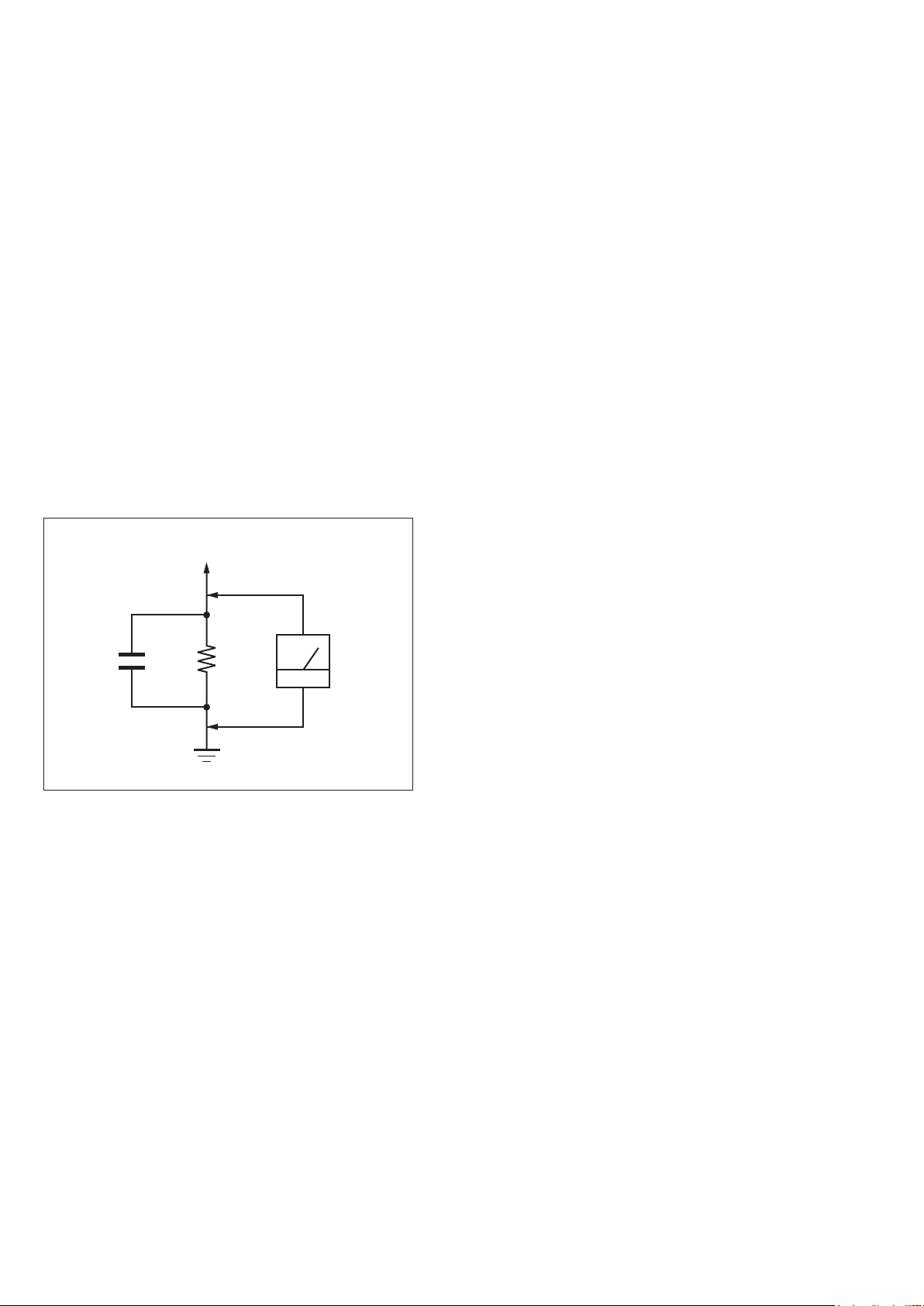
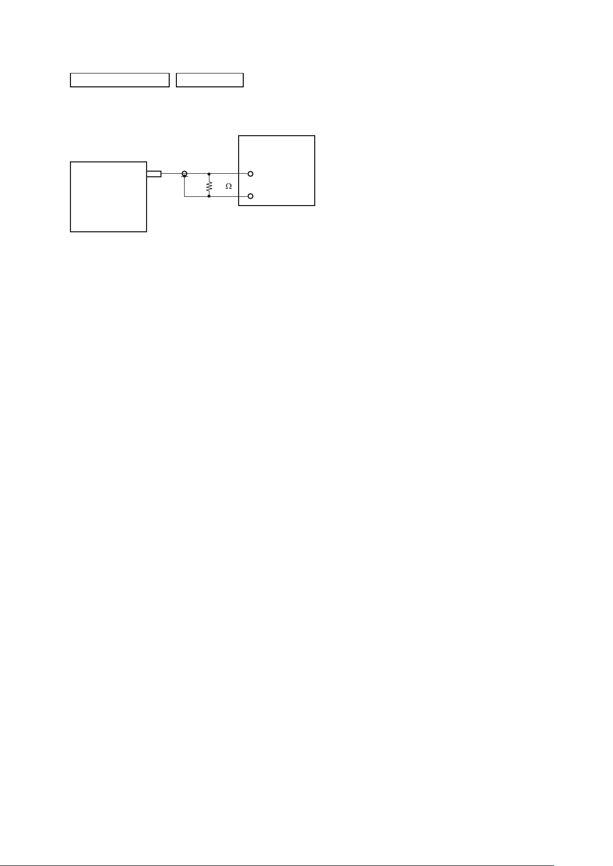
LEAKAGE TEST
The AC leakage from any exposed metal part to earth ground and
from all exposed metal parts to any exposed metal part having a
return to chassis, must not exceed 0.5 mA (500 microamperes).
Leakage current can be measured by any one of three methods.
1. A commercial leakage tester, such as the Simpson 229 or RCA
WT-540A. Follow the manufacturers’ instructions to use these
instruments.
2. A battery-operated AC milliammeter. The Data Precision 245
digital multimeter is suitable for this job.
3. Measuring the voltage drop across a resistor by means of a
VOM or battery-operated AC voltmeter. The “limit” indication
is 0.75 V, so analog meters must have an accurate low-voltage
scale. The Simpson 250 and Sanwa SH-63Trd are examples
of a passive VOM that is suitable. Nearly all battery operated
digital multimeters that have a 2V AC range are suitable. (See
Fig. A)
To Exposed Metal
Parts on Set
1.5 kΩ0.15 μF
Earth Ground
AC
voltmeter
(0.75 V)
Fig. A. Using an AC voltmeter to check AC leakage.
SAFETY-RELATED COMPONENT WARNING!
COMPONENTS IDENTIFIED BY MARK 0 OR DOTTED LINE
WITH MARK 0 ON THE SCHEMATIC DIAGRAMS AND IN
THE PARTS LIST ARE CRITICAL TO SAFE OPERATION.
REPLACE THESE COMPONENTS WITH SONY PARTS
WHOSE PART NUMBERS APPEAR AS SHOWN IN THIS
MANUAL OR IN SUPPLEMENTS PUBLISHED BY SONY.
2
Page 3

TABLE OF CONTENTS
HCD-SH2000
1. SERVICING NOTES ............................................. 4
2. DISASSEMBLY
2-1. Side Panel A, Side Panel B and Top Panel Section ........ 6
2-2. Back Panel Section ......................................................... 7
2-3. Front Panel Section ........................................................ 7
2-4. DMB21 Board ................................................................. 8
2-5. CDM Section .................................................................. 8
2-6. CD MECHANISM DECK BLOCK (1) ......................... 9
2-7. CD MECHANISM DECK BLOCK (2) ......................... 9
2-8. DAMP Board, MAIN Board ........................................... 10
2-9. SWITCHING REGULATOR ......................................... 10
3. TEST MODE ............................................................ 11
4. ELECTRICAL CHECK ......................................... 13
5. DIAGRAMS
5-1. Block Diagram - RS SERVO, USB Section - ................. 15
5-2. Block Diagram - MAIN Section - ................................... 16
5-3. Block Diagram - AMP Section - ..................................... 17
5-4. Block Diagram - PANEL, POWER SUPPLY Section - . 18
5-5. Printed Wiring Board
- MAIN Board (Component Side) (Suffi x 11) - .............. 20
5-6. Printed Wiring Board
- MAIN Board (Conductor Side) (Suffi x 11) - ............... 21
5-7. Printed Wiring Board
- MAIN Board (Component Side) (Suffi x 12) - ............. 22
5-8. Printed Wiring Board
- MAIN Board (Conductor Side) (Suffi x 12) - ............... 23
5-9. Schematic Diagram - MAIN Board (1/4) (Suffi x 11) - ... 24
5-10. Schematic Diagram - MAIN Board (2/4) (Suffi x 11) - ... 25
5-11. Schematic Diagram - MAIN Board (3/4) (Suffi x 11) - ... 26
5-12. Schematic Diagram - MAIN Board (4/4) (Suffi x 11) - ... 27
5-13. Schematic Diagram - MAIN Board (1/4) (Suffi x 12) - .. 28
5-14. Schematic Diagram - MAIN Board (2/4) (Suffi x 12) - .. 29
5-15. Schematic Diagram - MAIN Board (3/4) (Suffi x 12) - .. 30
5-16. Schematic Diagram - MAIN Board (4/4) (Suffi x 12) - .. 31
5-17. Printed Wiring Board
- DMB21 Board (Component Side) - ............................ 32
5-18. Printed Wiring Board
- DMB21 Board (Conductor Side) - ............................... 33
5-19. Schematic Diagram - DMB21 Board (1/3) - .................. 34
5-20. Schematic Diagram - DMB21 Board (2/3) - .................. 35
5-21. Schematic Diagram - DMB21 Board (3/3) - .................. 36
5-22. Printed Wiring Boards
- DAMP Board (Component Side) - ............................... 37
5-23. Printed Wiring Boards
- DAMP Board (Conductor Side) - ................................. 38
5-24. Schematic Diagram - DAMP Board (1/4) - .................... 39
5-25. Schematic Diagram - DAMP Board (2/4) - .................... 40
5-26. Schematic Diagram - DAMP Board (3/4) - .................... 41
5-27. Schematic Diagram - DAMP Board (4/4) - .................... 42
5-28. Printed Wiring Boards 5-29. Schematic Diagram -
5-30. Printed Wiring Boards - VOLUME Board- .................... 45
5-31. Schematic Diagram - VOLUME Board - ....................... 46
5-32. Printed Wiring Boards 5-33. Schematic Diagram 5-34. Printed Wiring Boards -
BOTTON LED AND TUNER Board - ........................... 49
DISPLAY Board - ................... 43
DISPLAY Board - ........................ 44
BUTTON, USB Board - .......... 47
BUTTON, USB Board - .............. 48
VOLUME LED,
5-35. Schematic Diagram -
BOTTON LED AND TUNER Board - ........................... 50
5-36. Printed Wiring Boards 5-37. Schematic Diagram 5-38. Printed Wiring Boards 5-39. Schematic Diagram -
VOLUME LED,
AUDIO-IN Board - ................. 51
AUDIO-IN Board - ...................... 51
MIC Board - ............................ 52
MIC Board - ................................. 52
6. EXPLODED VIEWS
6-1. Main Section ................................................................... 65
6-2. Front Panel Section (1) ................................................... 66
6-3. Back Panel Section ......................................................... 67
6-4. Chassis Section ............................................................... 68
6-5. CDM Section .................................................................. 69
7. ELECTRICAL PARTS LIST .............................. 70
3
Page 4
HCD-SH2000
Ver. 1.1
SECTION 1
SERVICING NOTES
Notes on chip component replacement
• Never reuse a disconnected chip component.
• Notice that the minus side of a tantalum capacitor may be
damaged by heat.
Flexible Circuit Board Repairing
• Keep the temperature of the soldering iron around 270 °C
during repairing.
• Do not touch the soldering iron on the same conductor of the
circuit board (within 3 times).
• Be careful not to apply force on the conductor when soldering
or unsoldering.
UNLEADED SOLDER
Boards requiring use of unleaded solder are printed with the
leadfree mark (LF) indicating the solder contains no lead.
(Caution: Some printed circuit boards may not come printed with
the lead free mark due to their particular size)
: LEAD FREE MARK
Unleaded solder has the following characteristics.
• Unleaded solder melts at a temperature about 40 °C higher
than ordinary solder.
Ordinary soldering irons can be used but the iron tip has to be
applied to the solder joint for a slightly longer time.
Soldering irons using a temperature regulator should be set to
about 350 °C.
Caution: The printed pattern (copper foil) may peel away if
the heated tip is applied for too long, so be careful!
• Strong viscosity
Unleaded solder is more viscous (sticky, less prone to fl ow)
than ordinary solder so use caution not to let solder bridges
occur such as on IC pins, etc.
• Usable with ordinary solder
It is best to use only unleaded solder but unleaded solder may
also be added to ordinary solder.
CAUTION
Use of controls or adjustments or performance of procedures
other than those specifi ed herein may result in hazardous radiation
exposure.
MODEL IDENTIFICATION
- BACK PANEL -
Model Part No.
E2, E51, EA, MY, SAF
MX
Abbreviation
•
E2 : 120 V AC area in E model
E51 : Chilean and Peruvian models
EA : Saudi Arabian model
MX : Mexican model
MY : Malaysia model
SAF : South African model
PLAYABLE DISC
Format of discs Logo
AUDIO CD
•
• CD-R/-RW in AUDIO
CD format
• CD-R/-RW in DATA CD
format, containing MP3
audio tracks 1) that
conforms to ISO 9660
2)
Level 1/Level 2, Joliet
(in expansion format), or
Multi Session
3)
PART No.
4-275-656-0[]
4-275-656-1[]
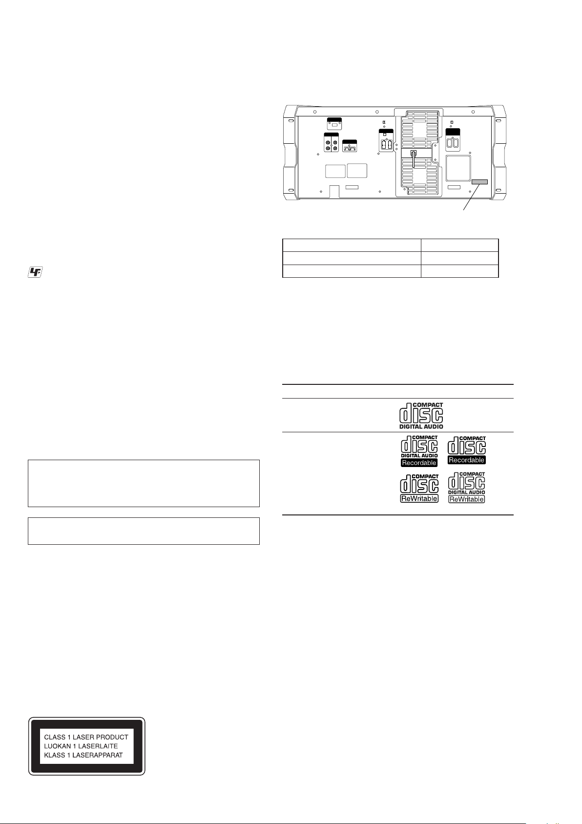
NOTES ON HANDLING THE OPTICAL PICK-UP BLOCK
OR BASE UNIT
The laser diode in the optical pick-up block may suffer electrostatic
break-down because of the potential difference generated by the
charged electrostatic load, etc. on clothing and the human body.
During repair, pay attention to electrostatic break-down and also
use the procedure in the printed matter which is included in the
repair parts.
The fl exible board is easily damaged and should be handled with
care.
NOTES ON LASER DIODE EMISSION CHECK
The laser beam on this model is concentrated so as to be focused
on the disc refl ective surface by the objective lens in the optical
pickup block. Therefore, when checking the laser diode emission,
observe from more than 30 cm away from the objective lens.
This appliance is
claassifi ed as a CLASS 1
LASER product. This
label is located on the
rear exterior.
4
1)
MP3 (MPEG 1 Audio Layer 3) is a standard format defi ned
by ISO/MPEG which compresses audio data. MP3 audio
tracks must be in MPEG 1 Audio Layer 3 format.
2)
A logical format of fi les and folders on CD-ROMs, defi ned
by ISO (International Organization for Standardization).
3)
This is a recording method that enables adding of data using
the Track-At-Once method. Conventional discs begin at a
disc control area called the Lead-in and end at an area called
Lead-out. A Multi Session disc is a disc having multiple
sessions, with each segment from Lead-in to Lead-out
regarded as a single session.
NOTE OF REPLACING THE IC102 AND IC4605 ON THE
DMB21 BOARD
IC102 and IC4605 on the DMB21 board cannot exchange with
single. When these parts on the DMB21 board are damaged,
exchange the entire mounted board.
NOTE OF REPLACEMENT OF THE MS-214 BOARD
When the MS-214 board is defective, exchange the entire MD
(AU) ASSY.
Page 5
MAIN BOARD DISCRIMINATION
In this set, the MAIN board has been changed in the midway of
production.
Repair after distinguishing each type set to doing the repair referring
to the following.
– MAIN Board (Component Side) –
SUFFIX-11 : 1-883-863-11
SUFFIX-12 : 1-883-863-12
NOTE OF REPLACING THE IC103 AND C242
(Combination: TYPE B) ON THE MAIN BOARD
(Suffi x-12)
IC103 and C242 (Combination: TYPE B) on the MAIN board
(Suffi x-12) cannot exchange with single. When these parts on
the MAIN board (Suffi x-12) are damaged, remove IC103 and
C242 (Combination: TYPE B) and replace with IC102 and C239
(Combination: TYPE A)
HCD-SH2000
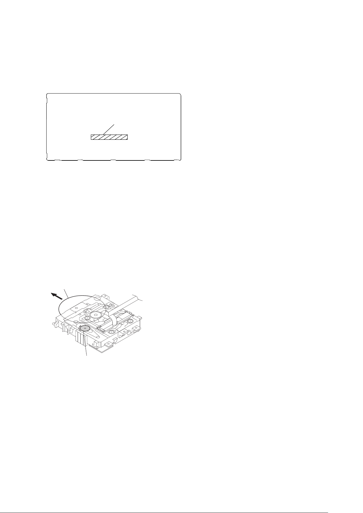
HOW TO EJECT THE DISC WHEN POWER SWITCH
TURNS OFF
Note: Please take out the CD mechanism block from a set
referring to “SECTION 2 DISASSEMBLY”.
disc
– CD mechanism block bottom view –
Please rotate the pully in the direction of the arrow and eject the disc.
5
Page 6
HCD-SH2000
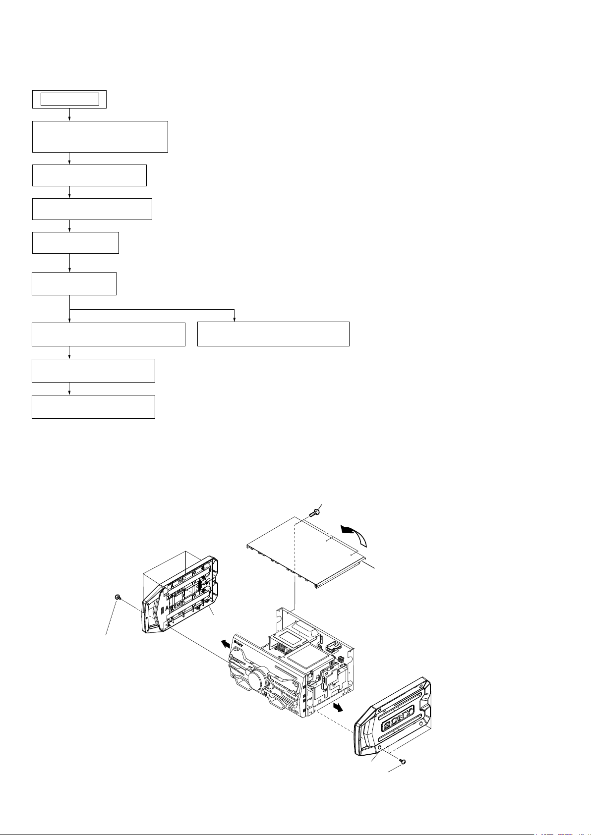
Note: Disassemble the unit in the order as shown below.
SET
2-1. SIDE PANEL A,SIDE PANEL B
AND TOP PANEL SECTION
(Page 6)
2-2. BACK PANEL SECTION
(Page 7)
2-3. FRONT PANEL SECTION
(Page 7)
2-4. DMB21 BOARD
(Page 8)
2-5. CDM SECTION
(Page 8)
SECTION 2
DISASSEMBLY
2-6. CD MECHANISM DECK BLOCK (1)
(Page 9)
2-8. DAMP Board, MAIN Board
(Page 10)
2-9. SWITCHING REGULATOR
(Page 10)
2-7. CD MECHANISM DECK BLOCK (2)
(Page 9)
Note: Follow the disassembly procedure in the numerical order given.
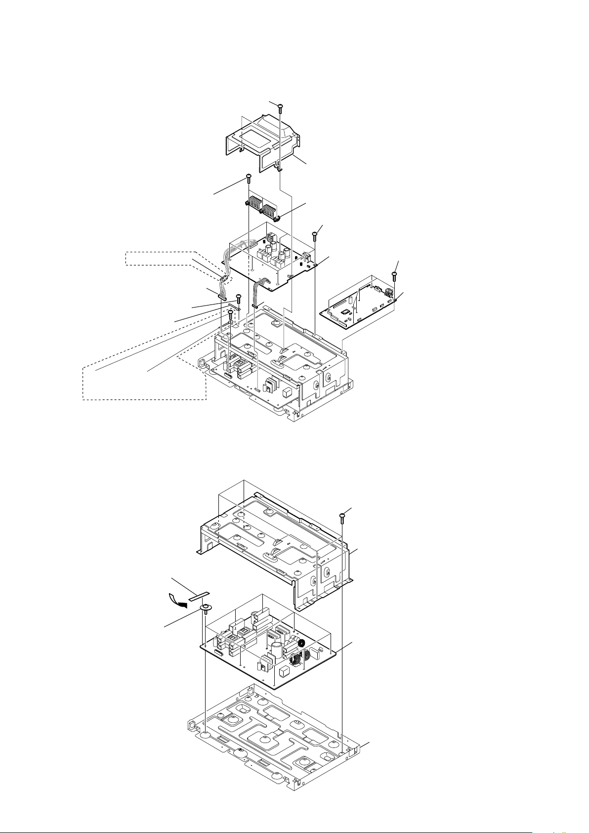
2-1. SIDE PANEL A, SIDE PANEL B AND TOP PANEL SECTION
7 three
(+BVTP 3
screws
10)
x
8
9 top panel section
3
side panel A
1 four
screws
(3.5 x 16)
2
5
6
side panel B
4 four
screws
(3.5 x 16)
6
Page 7
2-2. BACK PANEL SECTION
4 CN1404 (3P)
3 CN1405 (3P)
HCD-SH2000
1 twelve
(+BVTP 3
screws
x
Ver. 1.1
10)
2-3. FRONT PANEL SECTION
5
6 back panel section
2 wire (flat type) (7 core)
(CN703)
1 two
screws
(+BVTP 3
x
10)
(for SAF, EA only)
6
7 front panel section
2 eight
(+BVTP 3
screws
x
3 CN106 (7P)
4 wire (flat type) (23 core)
(CN105)
5 CN300 (14P)
10)
7
Page 8
HCD-SH2000
Ver. 1.1
2-4. DMB21 BOARD
(for SAF, EA only)
9 CN201 (6P)
q; CN302 (3P)
qa wire (flat type) (13 core)
(CN700)
8 wire (flat type) (7P core)
(CN202/CN203)
7 wire (flat type) (24 core)
(CN101)
qd shield plate bottom DMB21
qs DMB21 board
6 CN701 (7P)
2
4 four
1 four
(+BVTP 3
(+BV3 (3-CR))
screws
x
10)
5 wire (flat type) (13 core)
(CN702)
3 Shield plate top DMB21
screws
2-5. CDM SECTION
1 two
screws
(+BVTP 3
x
10)
2 cover CDM top
3 three
(+BVTP 3
7 two
(+BVTP 3
screws
x
10)
4 CD MECHANISM DECK BLOK
5 two
screws
(+BVTP 3
6 cover CDM bottom
screws
x
10)
x
10)
(for SAF, EA only)
8
8 CDM bracket
Page 9
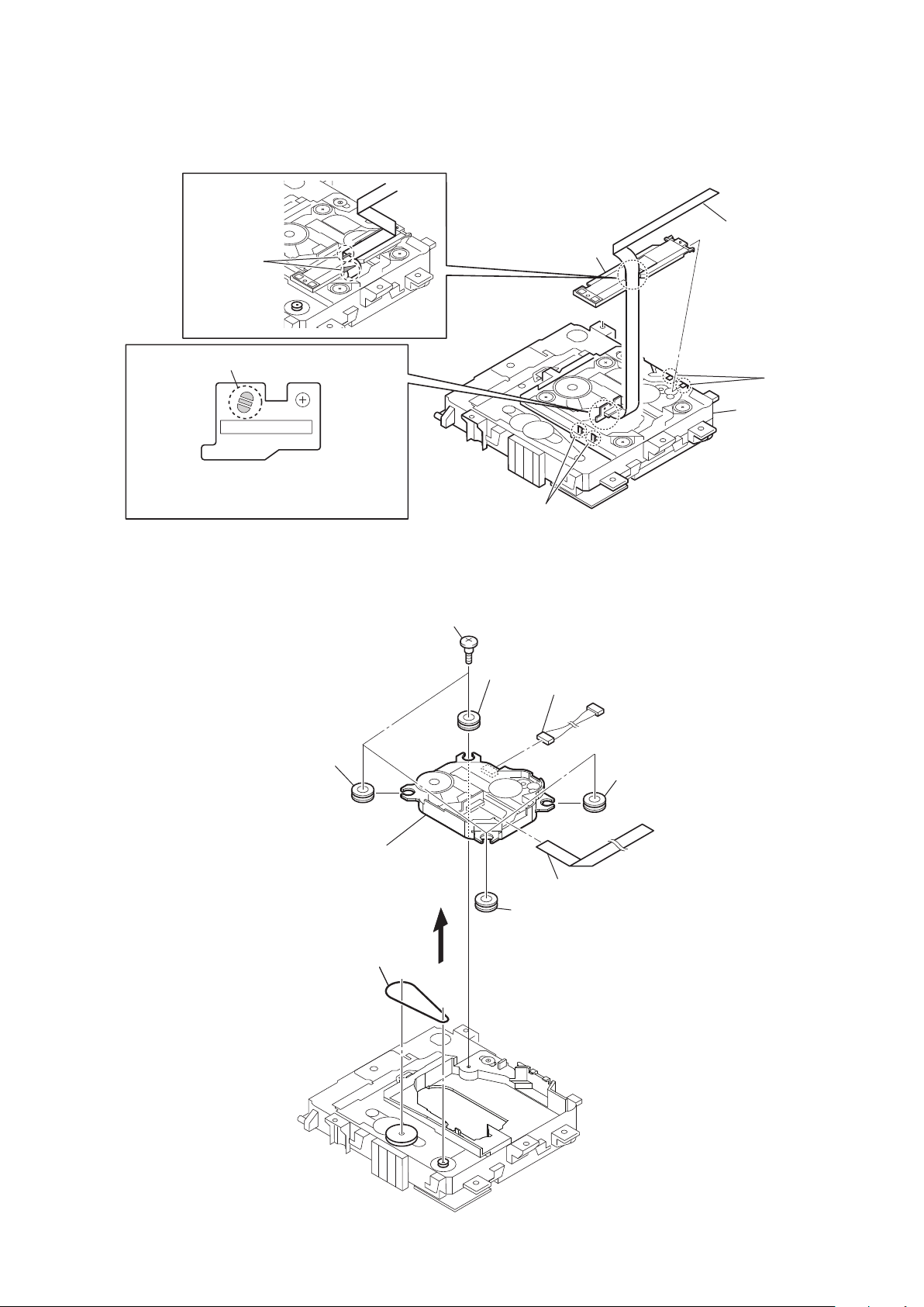
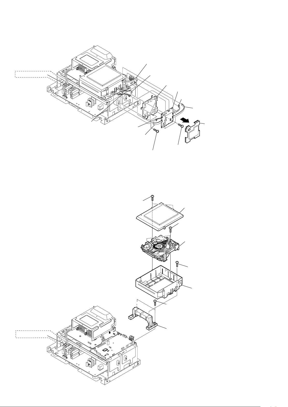
2-6. CD MECHANISM DECK BLOCK (1)
Note 1 : Before disconnecting the wire (fl at type) (24 core) of optical pick-up block, solder the short-land.
4
2
two claws
Solder the short-land.
5
Note 2: When assembling the optical pick-up block,
remove the solder of short-land after
connecting the wire (flat type) (24 core).
FFC holder
3 two claws
– CD mechanism deck block bottom view –
HCD-SH2000
6
wire (flat type)
(24 core) (CN101)
3 two claws
1 CD mechanism
deck block
2-7. CD MECHANISM DECK BLOCK (2)
four insulator screws
1
insulator
5
6
device, optical
(KHM-313CAB/CZRP)
belt (MOT)
7
belt (MOT)
2
insulator
5
insulator
5
connector
3
insulator
5
wire (flat type) (24 core)
4
– CD mechanism deck block bottom view –
9
Page 10
HCD-SH2000
Ver. 1.1
2-8. DAMP BOARD, MAIN BOARD
1 two
screws
(+BVTP 3
x
10)
2 bracket tunnel
3 three
(+BVTT 3
(for SAF, EA only)
6 CN2 (9P)
qa one
screw
(+BVTP 3
qsstopper wiring
qdone screw
(+BVTP 3x10)
qfstopper wiring
(for SAF, EA only)
x
2-9. SWITCHING REGULATOR
10)
screws
x
12 (S))
7 CN3 (6P)
4 heat sink DAMP
5 six
screws
(+BVTP 3
8 DAMP board
x
10)
9 six
screws
x
(+BVTP 3
q; MAIN board
10)
3saranet cushion
4 nine
screws
(SCREW, WASHER (M3))
1 four
screws
(+BV3 (3-CR))
2 sub chassis
5SWITCHING REGULATOR
6 chassis
10
Page 11

SECTION 3
TEST MODE
HCD-SH2000
PANEL TEST MODE
This mode is used to check the fl uorescent indicator tube, LEDs,
keys, [MASTER VOLUME] jog, model, destination and software
version.
Procedure:
1. Press [SEARCH] button and [OPTIONS] button simultaneously and hold 3 seconds.
2. All LEDs and segments in fl uorescent indicator tube will light
up.
3. When you want to enter to the software version display mode,
press [FLANGER] button. The model information appears on
the fl uorescent indicator tube. Press [FLANGER] button again
to view the destination information.
4. During the destination information display, press [FLANGER]
button. Each time [FLANGER] button is pressed, the fl uorescent
indicator tube shows the version of each category software in
the following sequence: SC, MTK (DMB Board fi rmware
version), UI, PF, SYS, CD, CDMA, CDMB, ST, TA, TAS, TM
and return back to model information display.
5. When [SEARCH] button is pressed while the version
numbers are being displayed except model and destination, the
date of the software creation appears. When [SEARCH] button
is pressed again, the display returns to the software version
display.
6. Press [ISOLATOR] button, the key check mode is activated.
7. In the key check mode, the fl uorescent indicator tube displays
“K 0 V0”. Each time a button is pressed, “K” value increases.
However, once a button has been pressed, it is no longer taken
into account.
“V” value increases in the manner of 0, 1, 2, 3 ... if [MAS-
TER VOLUME] knob is turned clockwise, or it decreases
in the manner of 0, 9, 8, 7 ... if [MASTER VOLUME] knob
is turned counterclockwise.
8. When [SOUND FLASH] button is pressed after all LEDs and
segments in fl uorescent indicator tube light up, alternate
segments in fl uorescent indicator tube and LEDs would light
up. If you press [SOUND FLASH] button again, another half
of alternate segments in fl uorescent indicator tube and LEDs
would light up. Pressing [SOUND FLASH] button again
would cause all segments in fl uorescent indicator tube and
LEDs light OFF. Pressing [SOUND FLASH] button again
would cause all segments in fl uorescent indicator tube and all
LEDs light up.
9. To release from this mode, press the [SEARCH] button and
[OPTIONS] button in the same manner as step 1, or disconnect
the power cord.
COMMON TEST MODE
This mode is used to check operations of the Amplifi er section.
Procedure:
To enter Common Test Mode
1. Press [USB/USB SELECT] button and [PRESET EQ] button
simultaneously and hold for 3 seconds.
2. The upper segments of fl uorescent indicator tube will blink.
The function is changed to TV and the volume is changed to
VOLUME MIN.
Check of Amplifi er
1. Press [PRESET EQ] button repeatedly until a message “GEQ
MAX” appears on the fluorescent indicator tube. GEQ
increases to its maximum.
2. Press [PRESET EQ] button repeatedly until a message “GEQ
MIN” appears on the fluorescent indicator tube. GEQ
decreases to its minimum.
3. Press [PRESET EQ] button repeatedly until a message “GEQ
FLAT” appears on the fl uorescent indicator tube. GEQ is set to
fl at.
4. When the [MASTER VOLUME] knob is turned clockwise
even slightly, the sound volume increases to its maximum and
a message “VOLUME MAX” appears on the fluorescent
indicator tube.
5. When the [MASTER VOLUME] knob is turned counterclockwise even slightly, the sound volume decreases to its minimum
and a message “VOLUME MIN” appears on the fl uorescent
indicator tube.
To release from Common Test mode
1. To release from this mode, press
button.
@/1
2. The cold reset is enforced at the same time.
COLD RESET
The cold reset clears all data including preset data stored in the
EEPROM to initial conditions. Execute this mode when returning
the set to the customer.
Procedure:
1. Press
2. Press [
button to turn on the system.
@/1
] button and
x
@/1
button simultaneously for 3
seconds.
3. “COLD RESET” appears on the fl uorescent indicator tube.
After that, the fl uorescent indicator tube becomes blank for a
while, and the system is reset.
TUNER STEP CHANGE
The step interval of AM channels can be toggled between 9
kHz and 10 kHz. This mode is not available for Saudi Arabian,
European and Russian models.
Procedure:
1. Press
button to turn on the system.
@/1
2. Press [FUNCTION] button repeatedly to select the “AM”.
3. Press
4. Press [ENTER] button and
button to turn off the system.
@/1
button simultaneously. The
@/1
system turns on automatically. The message “AM 9K STEP”
or “AM 10K STEP” appears on the fl uorescent indicator tube
and thus the channel step is changed.
CD SHIP MODE (WITH MEMORY CLEAR)
This mode moves the optical pick-up to the position durable to
vibration and clears all data including preset data stored in the
data flash to initial conditions during the next AC-In. Use this
mode when returning the set to the customer after repair.
Procedure:
1. Press
button to turn on the system.
@/1
2. Select CD function and without dics inserted.
@/1
3. Press [EJECT] button and
button simultaneously for 3
seconds. The system turns off automatically.
4. A message “MECHA LOCK” is displayed on the fl uorescent
indicator tube and the CD ship mode is set.
CD SHIP MODE (WITHOUT MEMORY CLEAR)
This mode moves the optical pick-up to the position durable to
vibration. Use this mode when returning the set to the customer
after repair.
Procedure:
5. Press
@/1
button to turn on the system.
6. Select CD function and without dics inserted.
7. Press [CD] button and
@/1
button simultaneously. The system
turns off automatically.
8. A message “MECHA LOCK” is displayed on the fl uorescent
indicator tube and the CD ship mode is set.
11
Page 12

HCD-SH2000
DISC THEFT PREVENTION MODE
This mode let prevent disc to be ejected. When this mode is
activated, the disc will not eject when [EJECT] button is pressed.
The message “LOCKED” will be displayed on the fl uorescent
indicator tube. This mode only applied when there is disc.
Procedure:
1. Press
2. Select CD function.
3. Press [PLAY/PAUSE] button and [EJECT] button simultaneously
for 3 seconds. The message “LOCKED” or “UNLOCKED”
displayed on the fl uorescent indicator tube.
FACTORY PRESET
This mode is use to load all the factory use preset frequencies
into FM 1-FM 20 and AM 1-AM 10. Originally, frequency of FM
1-FM 20 and AM 1-AM10 are set to the minimum frequency.
Procedure:
1. Press
2. Press [SEARCH] button and [TUNER/BAND] button simultaneously and hold for 3 seconds, message “FACTORY” appears
on the fl uorescent indicator tube. The function is changed to
TUNER automatically.
button to turn on the system.
@/1
button to turn on the system.
@/1
12
Page 13
SECTION 4
ELECTRICAL CHECK
HCD-SH2000
TUNER SECTION
FM AUTO STOP CHECK
set
Procedure:
1. Turn the power on.
2. Input the following signal from Signal Generator to FM
antenna input directly.
Carrier frequency : A = 87.5 MHz, B = 98 MHz, C = 108 MHz
Deviation : 75 kHz
Modulation : 1 kHz
ANT input : 35 dBu (EMF)
Note: Please use 75 ohm “coaxial cable” to connect SG and the
set. You cannot use video cable for checking.
Please use SG whose output impedance is 75 ohm.
0 dB = 1 ȝV
signal
generator
+
75
–
3. Set to FM tuner function and scan the input FM signal with
automatic scanning.
4. Confi rm that input Frequency of A, B and C detected and
automatic scanning stops.
The stop of automatic scanning means “The station signal is
received in good condition”.
13
Page 14
HCD-SH2000
• Circuit Boards Location
SECTION 5
DIAGRAMS
DAMP board
MS-214 board
TUNER
MAIN board
DMB21 board
DISPLAY board
BUTTON board
MIC board
BUTTON LED board
SWITCHING REGULATOR
14
VOLUME LED board
USB board
VOLUME board
AUDIO-IN board
Page 15
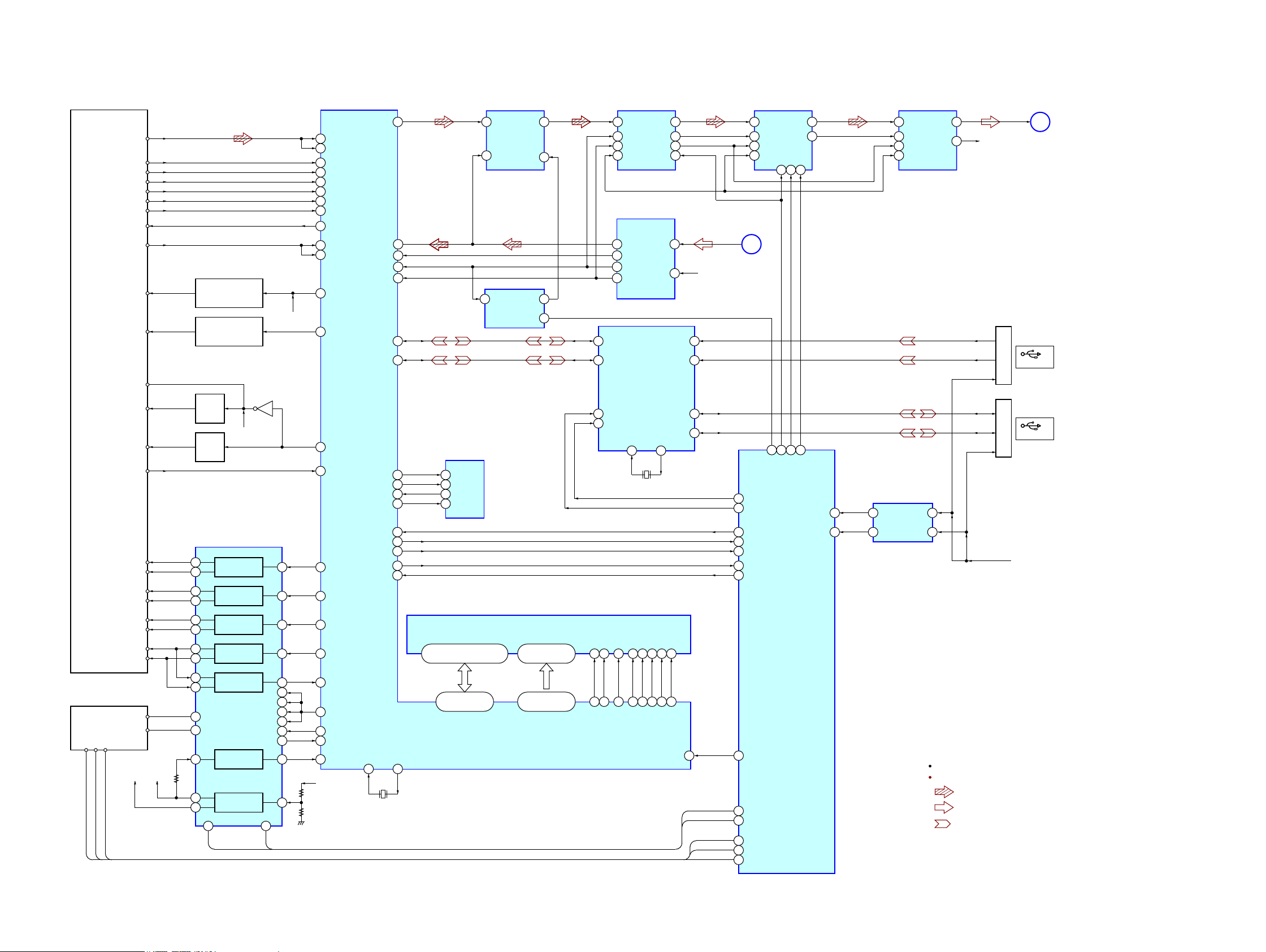
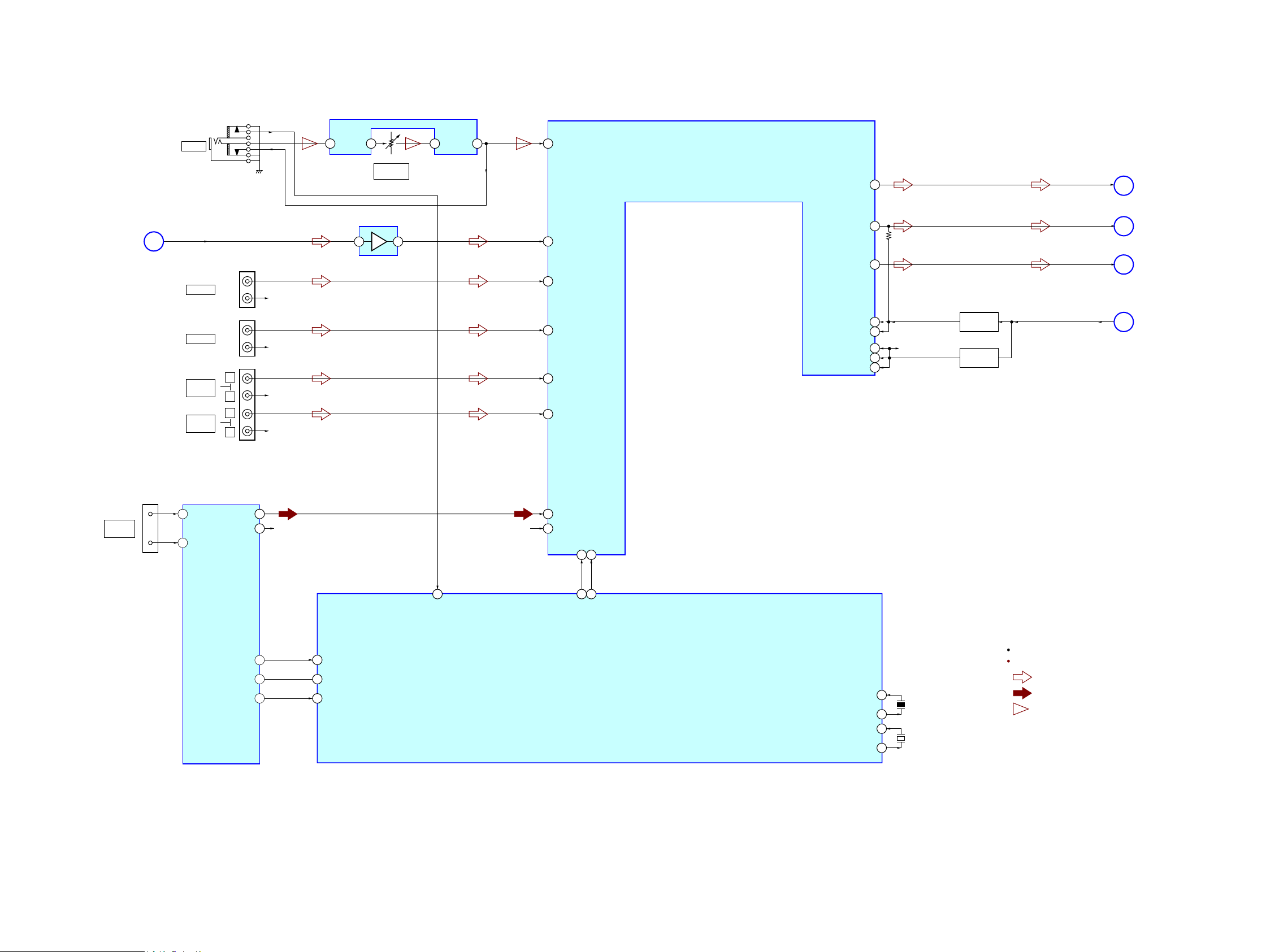
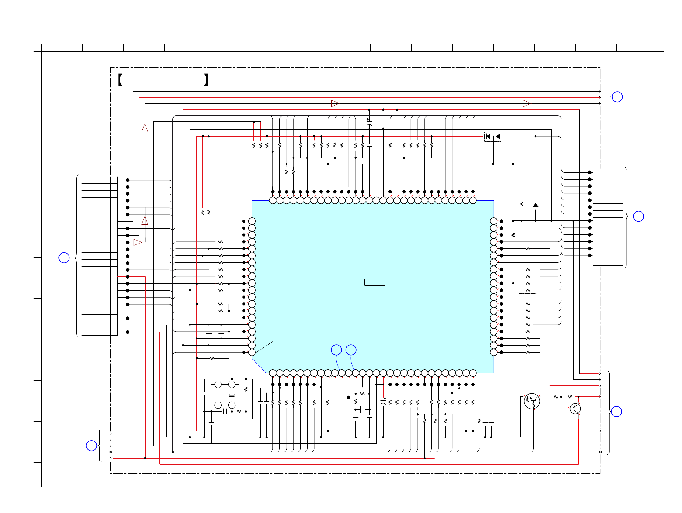
5-1. BLOCK DIAGRAM – RS SERVO, USB Section –
HCD-SH2000
VOA/A
VOB/B
VOC/C
VOD/D
DEVICE, OPTICAL
KHM-313CAB/C2RP
VR (780)
VR (650)
RF
PD
MSW
LIMIT
FCS+
FCS– 37
TRK+ 35
TRK– 34
SL+ 29
SL– 30
SP+ 27
SP– 28
AUTOMATIC POWER
CONTROL
Q102-1
AUTOMATIC POWER
CONTROL
Q102-2
CD ON
SWITCH
Q101-1
CD ON
SWITCH
Q101-2
FOCUS/TRACKING COIL DRIVE,
SPINDLE/SLED MOTOR DRIVE
36
COIL DRIVE
TRACKING
COIL DRIVE
MOTOR DRIVE
MOTOR DRIVE
Q103
REGO1
IC201
FOCUS
SLED
SPINDLE
REGO2
1
4
10
13
RF_IP125
OPOUT126
RF_C3
RF_B2
RF_A1
RF_D4
RF_F6VOE/E+G
RF_E5VOF/F+H
V2O12VC
MDI115
MDI216
LDO117LD (780)
LDO218LD (650)
RF AMP, SERVO DSP,
AUDIO PROCESSOR
MSW
23
118
GPIO
FOO25
TRO24
FMO21
DMO20
IC101
GPIO
GPIO19
GPIO
GPIO
GPIO
USB_DP 27
USB_DM 28
SF_CK
SF_CS#
SF_DI
SF_DO
IFSDI 35
IFSOD 41
IFSCK 40
IFCS# 88
IFBSY 87
MULTIPLEXER
IC4608
A
120
106
114
119
115
39
36
38
37
6
1
5
2
DG0, DQ1 – DQ15
2, 4, 5, 7, 8, 10, 11, 13, 42,
44, 45, 47, 48, 50, 51, 53
1
B
2
CK
15
D TYPE FLIP FLOP
SCK
CS_
SI
SO
IC102
FLASH ROM
IC4609
Y
5
SEL
6
Q
D
2
64M SDRAM
IC104
A0 – A11
23 – 26,
29 – 34, 22, 35
ASYNCHRONOUS SAMPLE
RATE CONVERTER
IC4607
SDIN
4
6
BCKI
LRCKI
5
2
RCKI
A/D CONVERTER
IC4601
9
DOUT
6
SCKI
7
LRCK
8
BCK
USBUP_DP
31
USBUP_DM
30
USB CONTROLLER
IC300
VBUS_DET27
RESET_N26
XTAL1/
CLKIN
33
X332
24MHz
20
21
38
15
39
SDOUT
LRCKO
BCKO
_RST
VINL
VINR
XTAL2
32
18
17
23
25
24
13
13
L-OUT
(Page 16)
14
R-CH
2USBDN1_DP
1USBDN1_DM
4USBDN2_DP
3USBDN2_DM
16
11
22
19
21
B
HUB_RST47
VBus_Det45
MTK-OSD35
MTK-SID36
MTK-CLK37
MTK-XIFCS41
MTK-BUSY40
DSP
IC4605
SDIN1
SCLKOUT2
SCLKOUT1
LRCK
MCLKO
32
38 79 77 78
DIGITAL-SEL
SYSTEM
CONTROLLER
IC100 (1/4)
SDOUT1
_RESET
SDA1
SCL1
15 16
DSP-CLK
DSP-DATA
/DSP-RESET
27
23
27/HUB-OC1
28/HUB-OC2
1
COMPARATOR
7
D/A CONVERTER
IC4602
DATA
2
BCK
1
LRCK
3
SCK
16
USB
IC301
VOUT L
VOUT L
3
5
VBUS
VBUS
R-CH
D+
D–
D+
D–
CN1150
3
2
1
CN1151
3
2
1
L-OUT
VBUS +5V
A
PLAY
REC/PLAY
(Page 16)
A
B
7
8
MS-214 BOARD
OCSW/REV
REW
HCD-SH2000
CKSW/FWD
TRG-SW
FWD
SW
LDM-
LDM+
REGO1
REGO2
46
47
24
25
41
31
32
DO5-
DO5+
REV
REV
BUFFER
BUFFER
REGULATOR
FWD
1617
PS
FWD
7
6
21
SPFG/OPINN12845
GPIOMUTE123 11619
MUTE4MUTE4 2220
GPIOTSD-M 9422
IOPMON/
12740
OPINP
RF +3.3V
45 – 49, 51 – 53,
64 – 61, 56 – 59
RD0 – RD15
XTALI
XTALO
9
10
82, 83, 85, 86,
74 – 69, 81, 67
RA0 – RA11
78
80
66
55
65
77
76
75
BA0 BA0
BA1 BA1
RCLK CLK
DQM0 LDQM
DQM1 UDQM
RAS# RAS
CAS# CAS
PRST #
RWE# WE
43
MTK-RST42
R-ch is omitted due to same as L-ch.
SIGNAL PATH
: AUDIO (DIGITAL)
8
X101
27MHz
REV
FWD
REW
FWD
SW
87
88
18
REV
FWR
OCSW86
CKSW85
TRG-SW
: AUDIO
: USB
1515
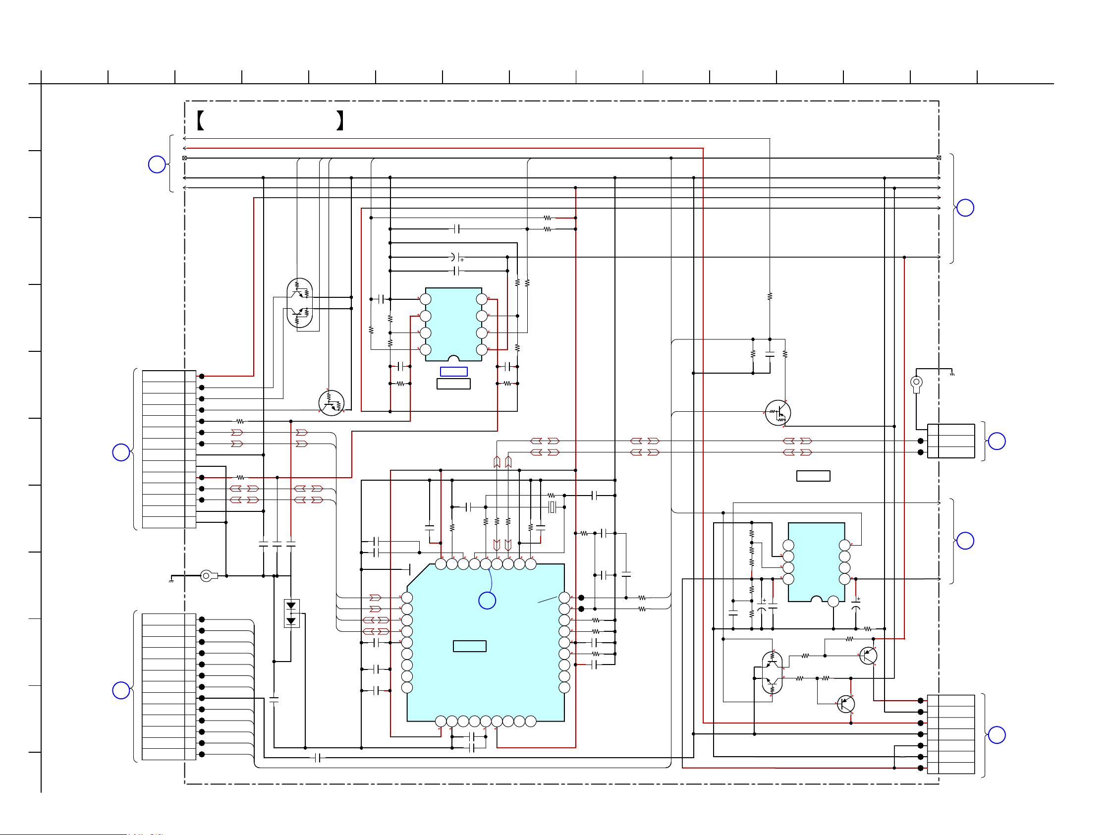
Page 16
HCD-SH2000
5-2. BLOCK DIAGRAM – MAIN Section –
IC1300 MIC AMP
(Page 15)
J1300
MIC IN
RV1300
MIC LEVEL
MIN MAX
IC501
OP AMP
A
L-OUT
TV
PC
GAME
AUDIO IN
DVD/SAT
AUDIO IN
J1200
R-CH
J1201
R-CH
J500
L
R
L
R
R-CH
R-CH
75
1375
46 MIC
39 GAME_L
43 TV IN-L
45 PC IN-L
40 GAME IN-L
42 DVD/SAT IN-L
INPUT SELECTOR,
ELECTRICAL VOLUME
IC500
BB2L
38INGAIN OUTL
26OUTL
25SWOUT
28BB1L
27
19
R-CH
18
17
BASS AGC
Q528
BASS AGC
Q518
L-OUT
SW OUT
BASS AGC
OUT
B
C
D
E
(Page 15)
(Page 17)
(Page 17)
(Page 17)
ANTENNA
FM/AM
4
6
TUNER (FM/AM)
FM ANT
AM ANT
IC1602
15
LOUT
ROUT
RDSI
R-CH
14 ST-R
80
MIC DET
DA
13
10
CK
8
24 ST-DATA
22 ST-CLK
20 ST-RDS
R-CH
41 ST-L
2
DATA22CLK
21
47
49
AUDIO CLK
AUDIO DATA
SYSTEM CONTROLLER
IC100 (2/4)
R-ch is omitted due to same as L-ch.
SIGNAL PATH
: AUDIO
15X-IN
X113
8MHz
13X-OUT
10XC-IN
11XC-OUT
X110
32.768kHz
: TUNER (FM/AM)
: MIC
HCD-SH2000
1616
Page 17
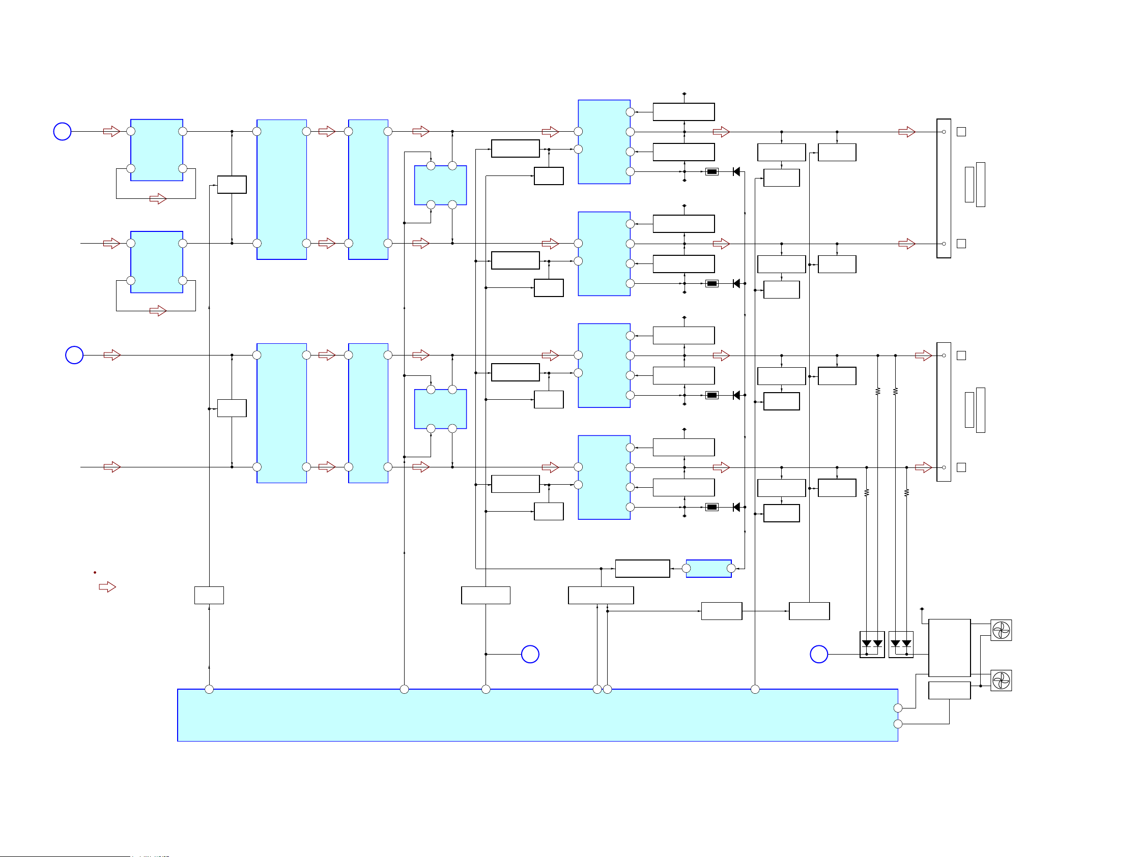
5-3. BLOCK DIAGRAM – AMP Section –
HCD-SH2000
D
(Page 16)
(Page 16)
AMPLIFIER CONTROLLER
IC1406
AMPLIFIER
IC502
Lch
R-CH
Lch
C
R-CH
5
7
5
7
INPUT+
OUTPUT
AMPLIFIER
INPUT+
OUTPUT
IC503
OUTPUT
INPUT+
OUTPUT
INPUT+
1
3
1
MUTE
Q601
3
OP AMP
5
INPUT+ OUTPUT
IC805
1
OUTPUTINPUT+
7
3
MUTE
Q600
3
OP AMP
5
INPUT+ OUTPUT
IC600
1
OUTPUTINPUT+
7
2
INB+ BOUT
5
2
5
INB+ BOUT
PREAMP
IC1403
PREAMP
IC1404
AOUTINA-
1
BUFFER
IC1410
75
BOUT
AOUT
INA+ INB+
13
7
1
AOUTINA-
7
BUFFER
IC1411
INA+ INB+
75
BOUT
AOUT
13
CEC DATA SWITCH
Q1412
CEC DATA SWITCH
Q1413
CEC DATA SWITCH
Q1411
CEC DATA SWITCH
Q1410
SWITCH
Q1414
SWITCH
Q1415
SWITCH
Q1416
SWITCH
Q1417
3
IN
VB
15
AMPLIFIER CONTROLLER
3
IN
VB
15
AMPLIFIER CONTROLLER
3
IN
VB
15
AMPLIFIER CONTROLLER
3
IN
VB
15
IC1407
IC1408
IC1409
COM
COM
COM
COM
HO
14
13
VS
LO
11
10
HO
14
13
VS
LO
11
10
HO
14
13
VS
LO
11
10
HO
14
13
VS
LO
11
10
+53V
DIGITAL AUDIO MOSFET
Q1422
DIGITAL AUDIO MOSFET
Q1423
-53V
+53V
DIGITAL AUDIO MOSFET
Q1418
DIGITAL AUDIO MOSFET
Q1419
-53V
+53V
DIGITAL AUDIO MOSFET
Q1420
DIGITAL AUDIO MOSFET
Q1421
-53V
+53V
DIGITAL AUDIO MOSFET
Q1424
DIGITAL AUDIO MOSFET
Q1425
-53V
TH1400
TH1401
TH1402
TH1403
D1420
D1419
D1418
D1417
RESONANCE DETECT
Q1430
SWITCH
Q1426
RESONANCE DETECT
Q1432
SWITCH
Q1428
RESONANCE DETECT
Q1433
SWITCH
Q1429
RESONANCE DETECT
Q1431
SWITCH
Q1427
DC PROTECTION
Q1443,1454
DC PROTECTION
Q1444,1455
DC PROTECTION
Q1445,1456
DC PROTECTION
Q1446,1457
TB1400
3
4
TB1401
3
4
L
LOW SPEAKER
R
L
HIGH SPEAKER
R
IMPEDANCE USE 4ȍ
IMPEDANCE USE 4ȍ
HCD-SH2000
SIGNAL PATH
: AUDIO
MUTE
Q207
/LINE-MUTE
26
DAMP-CLK
TRANSISTOR SWITCH
Q1407
/DAMP-RESET
G
SYSTEM CONTROLLER
IC100 (3/4)
OTW DRIVE / SD-SLOW DRIVE
Q1405
71697051
NO USE
/SD-SLOW
1717
OTP DRIVE
Q1469, 1470
COMPARATOR
IC1405
OUT -IN
12
DC PROTECTION
Q1449
75
RESONANCE
DC PROTECTION
Q1448
E
(Page 16)(Page 18)
D1403
FAN-EN
/FAN-LOCK
13V
FAN MOTOR DRIVE
Q1451, Q1441,
D1435
Q1439, Q1458,
Q1453, Q1476
FAN LOCK DETECT
Q1447
60
61
M101
DC FAN
DAMP FAN
M102
DC FAN
SMPS FAN
Page 18
HCD-SH2000
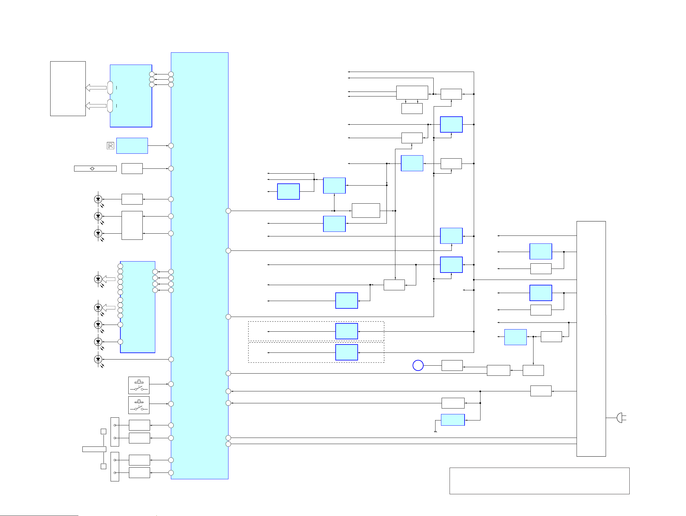
5-4. BLOCK DIAGRAM – PANEL, POWER SUPPLY Section –
FLUORESCENT INDICATOR
TUBE DRIVER
FL9001
FLUORESCENT
INDICATOR
TUBE
GRIDS 1-16
SEGMENTS 1-24
MASTER DJ CONTROL
D1151
(USB B : BLUE)
D1154
(USB B : RED)
D1150
(USB A : BLUE)
D1000 – D1005
(ILLUMINATION LED)
D1256 – D1259
(DJ LED)
D1280
(LED BAR2)
D1290
(LED BAR1)
D1251
(STANDBY LED)
IC901
GR1
GR16
34 – 49
SG1/KS1
SG24/KS24
10 – 33
REMOTE CONTROL
RECEIVER
IC982
S1000
ROTARY
ENCODER
LED DRIVE
Q303
LED DRIVE
Q301
Q12
15
Q11
16
Q10
17
Q9
18
Q8
19
Q7
20
Q4
23
Q3
24
Q1
1
2
Q2
22
Q5
21
Q6
SG4/KS4
SG3/KS3
SG2/KS2
LED DRIVE
IC1000
DATA
/OE
LATCH
CLOCK
1 2
2 1
3 21
4
5
6
8
FL-DRIVER-CLK
FL-DRIVER-DATA
/FL-DRIVER-CS
4 SIRCS
97
MASTER-VOL
100
USBB-LED-BLUE
95
USBB-LED-RED
USBA-LED-BLUE
82
LED-DRIVER-DATA
5
/LED-DRIVER-OE
6
LED-DRIVER-LATCH
3
LED-DRIVER-CLK
7
STBY-LED
89
SYSTEM CONTROLLER
IC100 (4/4)
MTK-POWER-CTL
VBUS-OE
/SD-FAST
SUB-ON
LED +13.5V
LED +13.5V
TD FL
TUBE
M +9V
VM +9V
D +9V
AVDD +5V
DVDD +5V
+3.3V
RF +3.3V
43
TU +3.3V
VBUS +5V
25
D 3.3V
DVDD +3.3V
DVDD +1.8V
58
72
MAIN BOARD (Suffix-11 and Suffix-12 (TYPE A))
EVER +4V
EVER +4V
MAIN BOARD (Suffix-12 (TYPE B))
REGULATOR
IC107
+5V
REGULATOR
IC804
+3.3V
REGULATOR
IC1601
REGULATOR
REGULATOR
REGULATOR
+1.8V
IC 111
+4V
IC102
+4V
IC103
SWITCHING
DRIVER
Q803
DC-DC CONVERTER
SWITCHING
Q805
(Page 17)
TRANSFOMER
T900
SWITCHING
Q906, Q907
SWITCHING
Q804
+9V
REGULATOR
IC803
G
SWITCHING
Q205, Q204
+9V
REGULATOR
IC800
SWITCHING
Q800, Q801
+5V
REGULATOR
IC802
+3.3V
REGULATOR
IC801
+13V
AMP RESET
Q1475
+53V
+18V
+5.0V
-18V
-5.0V
-53V
-40V
SD-FAST
Q1402, Q1460
-40V
REGULATOR
IC1402
+18V
REGULATOR
IC1400
+5.0V REG
Q1403
-18V
REGULATOR
IC1401
-5.0V REG
Q1401
OVP
Q1401
REGULATOR
Q1400
SWITCHING
REGULATOR
+VH
+VL
13V
-VL
-VH
HCD-SH2000
LED SPEAKER
S1250 – S1262
S1001 – S1013
CN705
3
L
4
CN704
3
R
4
LED DRIVE
Q604
LED DRIVE
Q605
LED DRIVE
Q606
LED DRIVE
Q607
68
AD-KEY-0
94
AD-KEY-1
SPK-L-LED-RED
52
SPK-L-LED-BLUE
53
SPK-R-LED-RED
54
SPK-R-LED-BLUE
55
AC-CUT
RESET
PCONT-MAIN
PCONT-SUB
19
12
63
59
μ COM RESET
Q200
μ COM RESET
IC101
BUFFER
Q203
AC-DET
(AC IN)
MAIN ON
SUB ON
Note: IC103 (TYPE B) on the MAIN board (Suffi x-12) cannot exchange with
single. When this part on the MAIN board (Suffi x-12) is damaged, remove
IC103 and C242 (Combination: TYPE B) and replace with IC102 and
C239 (Combination: TYPE A).
1818
Page 19
• Note for Printed Wiring Boards and Schematic Diagrams
HCD-SH2000
Ver. 1.1
Note on Printed Wiring Board:
• X : parts extracted from the component side.
• : parts extracted from the conductor side.
•
(The other layer’s patterns are not indicated.)
t Indication of transistor
• Abbreviation
E2 : 120 V AC area in E model
E51 : Chilean and Peruvian models
EA : Saudi Arabia model
MX : Mexican model
MY : Malaysia model
SAF : South African model
: Pattern from the side which enables seeing.
Caution:
Pattern face side:
(Conductor Side)
Parts face side:
(Component Side)
C
Q
B
E
D
Q
G
S
Q
B
CE
Q
B
CE
Parts on the pattern face side seen from
the pattern face are indicated.
Parts on the parts face side seen from
the parts face are indicated.
These are omitted.
These are omitted.
These are omitted.
These are omitted.
Note on Schematic Diagram:
• All capacitors are in μF unless otherwise noted. (p: pF)
50 WV or less are not indicated except for electrolytics
and tantalums.
• All resistors are in and 1/4 W or less unless otherwise
specifi ed.
•
• C : panel designation.
• A : B+ Line.
• B : B– Line.
• Voltage and waveforms are dc with respect to ground
under no-signal (detuned) conditions.
< > : CD PLAY
* : Impossible to measure
• Voltages are taken with a VOM (Input impedance 10 MΩ).
Voltage variations may be noted due to normal production
tolerances.
• Waveforms are taken with a oscilloscope.
Voltage variations may be noted due to normal production
tolerances.
• Circled numbers refer to waveforms.
• Signal path.
F : AUDIO
E : USB
f : TUNER
J : AUDIO (DIGITAL)
• Abbreviation
E51 : Chilean and Peruvian models
EA : Saudi Arabia model
MX : Mexican model
MY : Malaysia model
SAF : South African model
: nonfl ammable resistor.
2
Note: The components identifi ed by mark 0 or
dotted line with mark 0 are critical for safety.
Replace only with part number specifi ed.
no mark : TUNER
E2 : 120 V AC area in E model
HCD-SH2000
1919
Page 20
HCD-SH2000
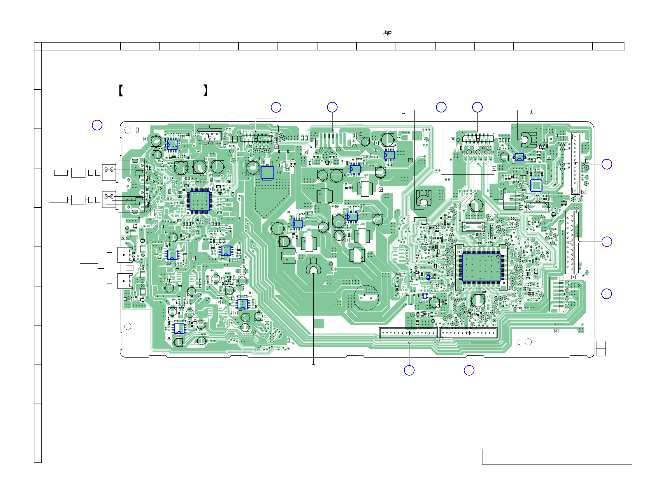
5-5. PRINTED WIRING BOARDS – MAIN BOARD (Component Side) (Suffi x-11) –
1 2 3 4 5 6 7 8 9 10 11 14 1512 13
A
MAIN BOARD (Component side)
B
TUNER
C
D
E
F
G
H
GAME
DVD/SAT
BOARD
CN1601
(Page 49)
AUDIO
IN
AUDIO
IN
L R
L R
LED
SPEAKER
J
IC501
C559
C558
C557
R870
J500
B1 E1C2
B2E2
13
C810
L
R
C811
CN704
Q604
13
CN705
C807
C808
F700
C806
C894
R740
R544
C723
R742
R741
C722
R739
C726
R867
C805
R747
C725
C605
R749
C724
R748
R743
C804
Q606
C1
R727
B1 E1C2
Q607
C1
B2E2
C809
B1 E1C2
C1
B2E2
C1
B2 E2
Q605
B1E1 C2
R728
R692
IC503
R725R726
C513
R696
C697
IC805
R546
R869
R840
R698
R662
C662
R853
‚W
‚P ‚S
R545
C503
C620
R697
‚T
‚W
C694
C778
R852
C782
R551
R548
R549
C565
C568
R751
7
R557
C566
‚T
C564
R552
C562
R558
C567
R547
C561
R550
C651
C554
C556
R502
C501
C502
C509
R509
C615
C617
R518
R612
R620
C698
C691
‚P ‚S
C686
R688
C687
R690
R762
R658
C657
R793
R788
R791
C770
B1 E1C2
R790
R851
R850
‚T
‚W
‚P ‚S
C893
C783
CN703
6
R559
R560
C649
C570
C551
C549
C880
114
56
15
R521
C522
C521
C518
R519
R619
Q518
R542
R848
R691
R689
R659
R657
C661
R792
C769
C1
Q601
B2E2
C777
R789
C780
R798
R799
1
2
FB750
C754
R763
C548
C547
C545
C546
C648
43
42
28
29
C524
R522
C887
C886
C543
C542
R541
C541
C540
C533
IC500
C629
R626
R526
C627
C528
R528
Q528
R628
R847
R678
C680
R677
R839
R857
IC502
R679
‚T
C678
R680
‚W
C676
C761
R785
B1 E1C2
C768
R787
R784
R854
R856
2
CN702
1
L751
C825
C583
C674
R676
‚P ‚S
R675
R674
C660
R673
C659
Q600
R797
C760
C1
B2E2
R782
C771
C767
R786
R783
C772
R796
R795
C776
‚T
IC600
C774
R794
‚W
‚P ‚S
C892
C784
C884
• See page 14 for Circuit Boards Location.
F
CN701
‚a ‚d
B1E1 C2
Q805
R835
R834
C834
C874
DMB21
BOARD
CN602
(Page 32)
1
R836
C841
IC802
R844
C836
R855
C843
8
1
C802
C840
8
1
C801
R843
C833
12
13
C813
3
IC803
C885
I
R822
C812
R821
R818
C847
12
IC800
C826
C873
L806
DMB21
BOARD
CN4604
(Page 32)
R817
Q800
Q801
‚a ‚d
R819
R820
C828
1
R842
C800
C823
R543
R745
R744
7
Q804
R841
‚a ‚d
Q803
R830
B2 E2
C1
R831
C875
L808
R804
R803
C829
R801
R802
58
C831
4
L803
ET800
• : Uses unleaded solder.
DMB21
BOARD
E
CN1108
(CHASSIS) (CHASSIS)
C748
R827
C850
R826
R815
R812
C844
R814
5
4
L805
R808
C837
R806
R807
5
4
L804
L807
C820
C852
R828
C851
5
8
R825
R824
R816
R810
1
C846
IC804
4
R823
ET302
IC801
R125
R239
JL520
R231
CN102
D231
Q200
R243
R242
R224
R222
R602
R135
R136
R137
C231
IC101
IC102
C241
C239
D267
C803
C821
R123
R126
D602
R128
R229
R127
R230
R603
R138
C233
C232
C238
R167
D167
C839
Q207
R263
R264
R262
C250
114
(Page 32)
2
1
C707
R118
R120
R121
R119
R122
R124
C124
C126
R226
C128
C226
R227
C127
R225
R129
R130
RB131
R134
RB140
R241
R232
D232
R233
Q203
R236
C240
R237
R238
C237
C267
1
30
31
50
51 80
R146
D233
R159
R158
CN100
D
CN700
X113
IC100
R160
R161
R113
C116
C163
R261
DMB21
BOARD
CN109
(Page 32)
12
C216
C112
X110
C111
R213
R111
C113C115
R110
C165
C162
ET300
R343
R341
13
R337
C341
R339
C339
IC301
C337
JL105
C110
R109
1
R163
14
‚T‚W
C338
C426
R426
R326
R327
C326
JL327
C327
JL326
R328
CN302
1
R105R107
C105
R104
R103
C102
R102
R100
C100
Q204
100
C298
C198
81
R178
R177
R172
R272
R175
C342
‚P ‚S
R342
R340
C311
R338
C340
C411
R322
C321
C415
C323
R325
R324
C328
R332
R333
JL350
R330
R331
C332
JL351
X332
Q205
‚a‚d
R258
R259
R194
R197
R294
R190
R290
C192
R186
R189
R285
RB185
R184
R180
R527
R278
R277
R171
R271
R174
R274
R170
C347
D704
R344
C310
C305
IC300
R335
C334
C435
C345
C346
C344
15
FB302
JL311
FB300
USB
BOARD
C
NO1152
(Page 47)
CN300
CN105
1
23
22
C336
Q303
C335
Q301
VOLUME
BOARD
A
CN1000
(Page 45)
2
1
7
AUDIO-IN
CN106
BOARD
H
NO1200
(Page 51)
1
11
1-883-863-
(11)
I
J
HCD-SH2000
(CHASSIS)
G
DAMP
BOARD
CN1400
(Page 37)
B
DAMP
BOARD
CN1401
(Page 37)
Note: Refer to the servicing notes “MAIN BOARD DISCRIMINATION”
(page 5) for how to distinguish SUFFIX-11 and SUFFIX-12.
2020
Page 21
HCD-SH2000
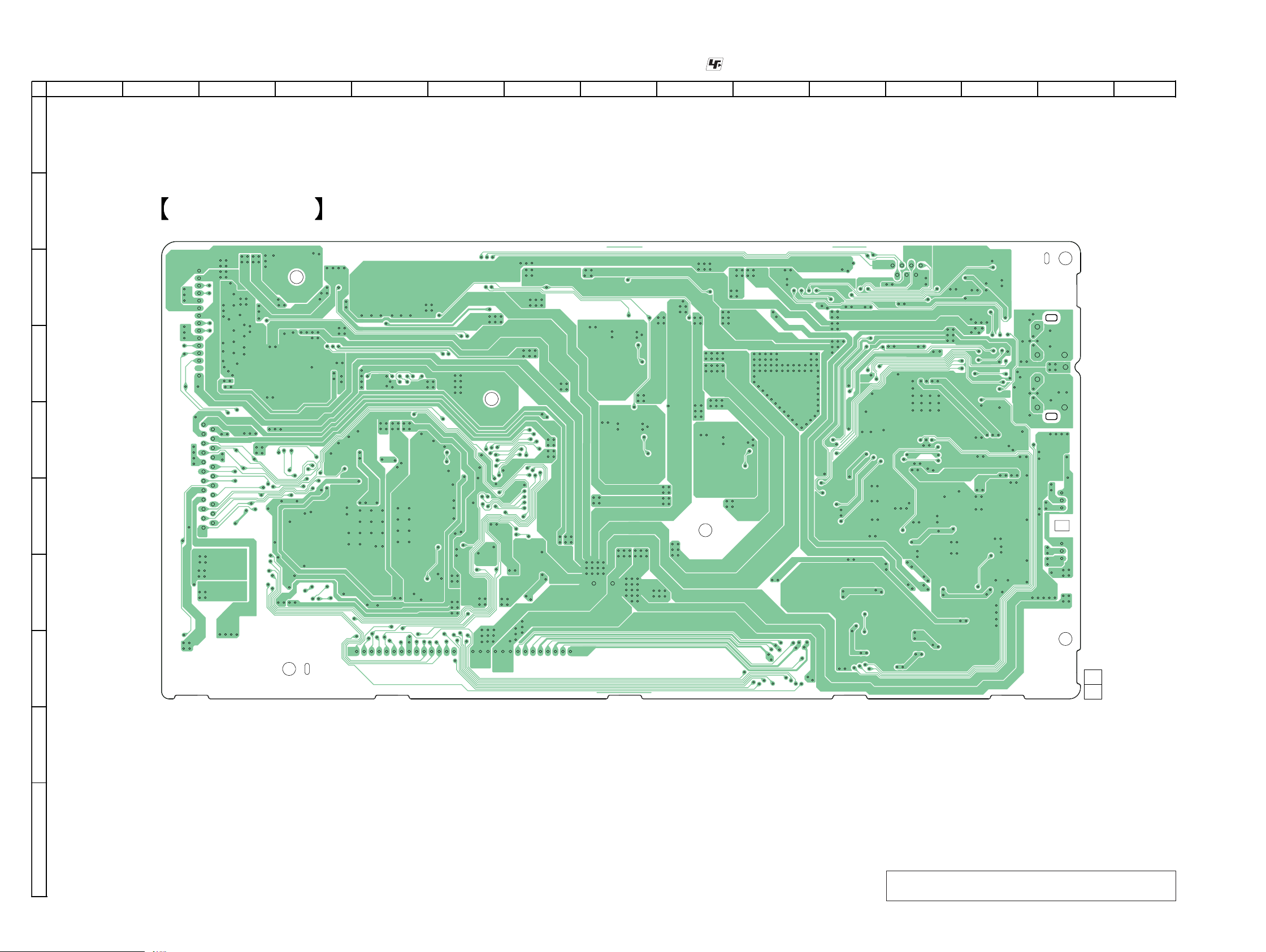
5-6. PRINTED WIRING BOARDS – MAIN BOARD (Conductor Side) (Suffi x-11) –
1 2 3 4 5 6 7 8 9 10 11 14 1512 13
A
B
MAIN BOARD (Conductor side)
C
D
• See page 14 for Circuit Boards Location.
• : Uses unleaded solder.
E
F
G
H
11
1-883-863-
(11)
I
J
HCD-SH2000
Note: Refer to the servicing notes “MAIN BOARD DISCRIMINATION”
(page 5) for how to distinguish SUFFIX-11 and SUFFIX-12.
2121
Page 22
HCD-SH2000
5-7. PRINTED WIRING BOARDS – MAIN BOARD (Component Side) (Suffi x-12) –
1 2 3 4 5 6 7 8 9 10 11 14 1512 13
A
MAIN BOARD (Component side)
B
TUNER
C
D
E
F
G
H
GAME
DVD/SAT
BOARD
CN1601
(Page 49)
AUDIO
IN
AUDIO
IN
L R
L R
LED
SPEAKER
J
IC501
C558
R870
J500
B1 E1C2
B2E2
13
C810
L
R
C811
CN704
Q604
13
CN705
C807
C808
F700
C806
C894
R740
R544
C723
R742
R741
C722
R739
C726
R867
C805
R747
C725
C605
R749
C724
R748
R743
C804
Q606
C1
R727
B1 E1C2
Q607
C1
B2E2
R696
R728
C697
R692
C809
B1 E1C2
IC503
C1
B2E2
R725R726
C1
B2 E2
Q605
B1E1 C2
IC805
R551
R548
R549
C565
C568
R751
7
R557
C566
‚W
‚T
C559
C557
C513
R869
R840
R662
C662
R853
‚P ‚S
R546
C503
R697
R698
C694
C778
R852
C782
C564
R552
C562
R558
C567
R547
C561
R550
R545
C651
C554
R502
C501
C502
C509
R509
C615
C617
R518
C620
R612
R620
C698
‚T
C691
‚W
‚P ‚S
C686
R688
C687
R690
R762
R658
C657
R793
R788
R791
C770
B1 E1C2
R790
R851
R850
‚T
‚W
‚P ‚S
C893
C783
CN703
6
R559
R560
C649
C570
C551
C556
C769
C1
Q601
B2E2
R789
C549
C880
114
56
15
R521
C522
C521
C518
R519
R619
Q518
R542
R848
R691
R689
R659
R657
C661
R792
C777
C780
R798
R799
1
2
FB750
C754
R763
C548
C547
C545
C543
C546
C542
C648
R541
43
C541
42
C540
C533
28
R522
C887
C886
IC500
29
C629
C524
R626
R526
C627
C528
R528
Q528
R628
R847
R678
C680
R677
R839
R857
IC502
R679
‚T
C678
R680
‚W
C676
C761
R785
B1 E1C2
C768
R787
R784
R854
R856
2
CN702
1
L751
C825
C583
C674
R676
‚P ‚S
R675
R674
C660
R673
C659
Q600
R797
C760
C1
B2E2
R782
C771
C767
R786
R783
C772
R796
R795
C776
‚T
IC600
C774
R794
‚W
‚P ‚S
C892
C784
C884
• See page 14 for Circuit Boards Location.
12
13
C813
3
IC803
C885
I
R822
C812
R821
R818
C847
12
IC800
C826
C873
L806
DMB21
BOARD
CN4604
(Page 32)
R817
Q800
Q801
‚a ‚d
R819
R820
C828
1
R842
C800
C823
R543
R745
R744
7
Q804
R841
‚a ‚d
Q803
R830
B2 E2
C1
R831
C875
L808
R804
R803
C829
R801
R802
58
C831
4
L803
ET800
CN701
‚a ‚d
F
Q805
R835
B1E1 C2
R834
C834
R836
C841
C874
R855
DMB21
BOARD
CN602
(Page 32)
1
C843
8
1
C802
IC802
C840
R844
C836
8
1
C801
R843
• : Uses unleaded solder.
DMB21
BOARD
E
CN1108
(CHASSIS) (CHASSIS)
C748
R827
C850
R826
R815
C844
R812
R816
R814
5
4
L805
R808
C837
R806
R810
R807
5
4
L804
C833
L807
C820
C852
R828
C851
5
8
R825
R824
1
C846
IC804
4
R823
ET302
IC801
R125
C242
R136
R137
D231
Q200
C231
R231
TYPE A
IC102
JL520
CN102
R224
R123
R222
R126
R602
R135
IC101
C241
C239
D267
D167
C803
C821
D602
R128
R229
R127
R230
R603
R138
C233
C232
C238
R167
C839
Q207
R263
R264
R262
C250
TYPE B
IC103
114
(Page 32)
2
1
C707
R118
R120
R121
R119
R122
R124
C124
C126
C128
R226
C226
R227
C127
R225
R129
R130
RB131
R134
RB140
R241
R232
D232
R233
Q203
R236
C240
R237
R238
C237
C267
1
30
31
50
51 80
R146
D233
R159
R158
CN100
D
CN700
X113
IC100
R160
R161
R113
C116
C163
R261
DMB21
BOARD
CN109
(Page 32)
12
C216
C112
X110
C111
R213
R111
C113C115
R110
C165
C162
ET300
R343
R341
13
R337
C341
R339
C339
IC301
C337
JL105
C110
R109
1
R163
14
‚T‚W
C338
C426
R426
R326
R327
C326
JL327
C327
JL326
R328
CN302
1
R105R107
C105
R104
R103
C102
R102
R100
C100
Q204
100
C298
C198
81
R172
R272
C342
‚P ‚S
R342
R340
C311
R338
C340
C411
R322
C321
C415
C323
R325
R324
C328
R332
R333
JL350
R330
R331
C332
JL351
X332
Q205
‚a‚d
R258
R259
R194
R197
R294
R190
R290
C192
R186
R189
R285
RB185
R184
R180
R527
R278
R178
R177
R277
R171
R271
R174
R274
R170
R175
C347
D704
R344
C310
C305
IC300
R335
C334
C435
C345
C346
C344
15
FB302
JL311
FB300
USB
BOARD
C
NO1152
(Page 47)
CN300
CN105
1
23
22
C336
Q303
C335
Q301
VOLUME
BOARD
A
CN1000
(Page 45)
2
1
7
AUDIO-IN
CN106
BOARD
H
NO1200
(Page 51)
1
12
1-883-863-
(12)
I
J
HCD-SH2000
Note 1: Refer to the servicing notes “MAIN BOARD
DISCRIMINATION” (page 5) for how to distinguish
SUFFIX-11 and SUFFIX-12.
(CHASSIS)
DAMP
BOARD
CN1400
(Page 37)
Note 2: A part of circuit composition of MAIN board (Suffi x-12) has been changed in the
midway of production. MAIN board (Suffi x-12) that has not been changed appears
as TYPE A, and the changed MAIN board (Suffi x-12) appears as TYPE B.
2222
G
B
DAMP
BOARD
CN1401
(Page 37)
Note 3: IC103 and C242 (Combination: TYPE B) on the MAIN board (Suffi x-12) cannot exchange
with single. When these parts on the MAIN board (Suffi x-12) are damaged, remove IC103
and C242 (Combination: TYPE B) and replace with IC102 and C239 (Combination: TYPE A).
Page 23
HCD-SH2000
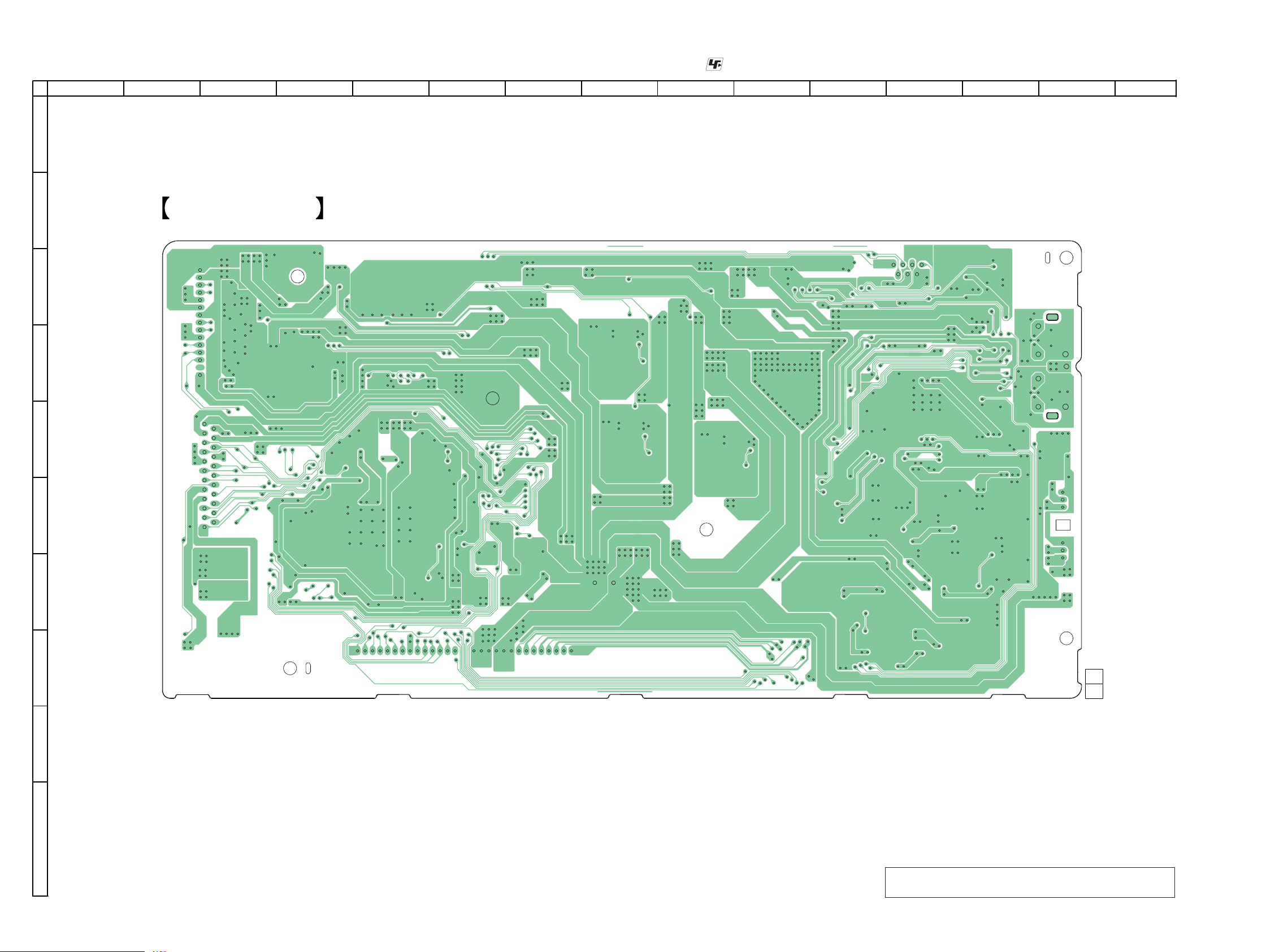
5-8. PRINTED WIRING BOARDS – MAIN BOARD (Conductor Side) (Suffi x-12) –
1 2 3 4 5 6 7 8 9 10 11 14 1512 13
A
B
MAIN BOARD (Conductor side)
C
D
• See page 14 for Circuit Boards Location.
• : Uses unleaded solder.
E
F
G
H
12
1-883-863-
(12)
I
J
HCD-SH2000
Note: Refer to the servicing notes “MAIN BOARD DISCRIMINATION”
(page 5) for how to distinguish SUFFIX-11 and SUFFIX-12.
2323
Page 24
HCD-SH2000
Ver. 1.1
5-9. SCHEMATIC DIAGRAM – MAIN BOARD (1/4) (Suffi x 11) –
1234567891011 141512 13
A
MAIN BOARD
(1/4)
B
C
CN105
D
E
F
G
A
VOLUME
BOARD
CN1000
(Page 46)
AD-KEY-1
MASTER-VOL
LED-DRIVER-CLK
LED-DRIVER-LATCH
LED-DRIVER-OE
LED-DRIVER-DATA
MIC-GND
A+9V
MIC-SIGNAL
MIC-DET
STBY-LED
AD-KEY-0
SIRCS
D+3.3V
EVER+3.3V
/FL-DEIVER-CS
FL-DRIVER-DATA
FL-DRIVER-CLK
LED-GND
D-GND
LED+13.5V
23P
JL211
1
JL212
2
JL213
3
JL214
4
JL215
5
JL216
6
7
JL217
8
JL218
9
JL219
10
JL220
11
JL221
12
JL222
13
JL223
14
JL224
15
JL225
16
JL226
17
JL227
18
JL228
19
20
JL229
-VG
21
22
JL230
23
94
97
7
3
6
5
R186 10k
C298
0.1
RB185
100
R285 10k
*1 R190
*2 R290
C198
8282
93
84
85
80
86
89
87
68
88
4
89
21
92
1
2
94
9595
97
100100
H
C110
22p
I
J
MAIN
BOARD
(2/4)
(Page 25)
5
4
8
1
7
6
50V
• See page 53 for Waveforms. • See page 61 for IC Pin Function Descriptions.
IC100
C163
0.1
VCC1
63
100R163
JL163
VSS
VCC2
PCONT-MAIN
AC-CUT
NMI
TRG-SW
JL118
JL119
JL120
16VC216 100
47kR119
100R118
18
19
*1 R190
4.7K - SAF, EA
1k
- E2, E51, MX
*2 R290
330 - SAF
1k - EA
4.7k - E2, E51, MX
0 - MY
100R184
100R189
15kR294
470R194
0.1
10kR197
4
X110
32.768kHz
3
C111
22p
50V
C116
0.1
78
80
10kR180
1.5kR278
1.5kR277
JL180
0
JL181
81
1.3
JL182
JL183
JL184
JL185
JL186
JL187
JL188
JL189
JL190
JL191
JL192
JL193
JL194
JL195
JL197
JL200
2
1
R111
220k
R110
10M
3.2
3.2
0.4
2.8
1.4
3.4
3.4
3.4
3.2
1.3
USBA-LED-BLUE
82
0
83
TRYOPENPWM
84
CKSW
85
OCSW
86
0
REV
87
0
FWR
88
0
STBY-LED
89
DEST-IN
90
0
91
MTK-POWER-MONITOR
92
0
93
AD-KEY-1
94
0
USBB-LED-RED
95
0
Avss
96
MASTER-VOL
97
VREF
98
AVCC
99
100
50V100pC102
1
JL101
50VC100 100p
470R100
1
77
100R527
100R178
JL179
JL178
DSP-CLK
/DSP-RESET
MIC-DETECT
USBB-LED-BLUE
FL-DRIVER-CLK3LED-DRIVER-LATCH4SIRCS5LED-DRIVER-DATA
FL-DRIVER-DATA
2
2.7 3.2 3.2
JL102
JL103
JL104
470R102
100R103
3
2
4
75
10kR271
10kR272
10kR175
100R177
JL176
JL175
JL177
DSP-DATA
100R104
JL174
JL173
RESONANCE
/LED-DRIVER-OE
LED-DRIVER-CLK
BYTE9CNVss
6
7
8
3.2
0 0 0 0 0 0
JL105
JL106
JL107
100R107
100R105
5
7
6
707968
71
100R171
JL171
/SD-SLOW
69
C162
100
16V
15kR274
470R174
100R170
JL170
JL169
NO USE
/DAMP-RESET
0.47
C165
JL168
JL167
3.3 03.4 3.4 0 3.23.23.23.23.2 3.02.9 3.2 0.8
AD-KEY-0
MIC-DATA-IN
72
100
R172
JL172
/SD-FAST
IC100
SYSTEM CONTROL
R5F3650KBDFA
1 2
Xcin
Xcout
RESET
X-OUT
VSS
R213
X113
8MHz
X-IN
1MR113
0
C115
22p
50V
10 11 12 13 14 15 16 17 18 19 20 21 22 23 24 25 26 27 28 29 30
2.9
1.2 3.2 1.7 1.6 3.2 3.2 3.2 3.1 3.3 3.3 3.3 1.6 0.6 3.3 3.4 3.43.10
1.1
150k
R109
JL112
C113
27p
50V
61
100R161
JL161
/FAN-LOCK
ST-RDS
100
R120
20
59
60
100R159
100R160
JL159
JL160
FAN- EN
/FL-DRIVER-CS
JL121
JL122
220R121
100
R122
21
22
PCONT-SUB
ST-CLK
R222
4.7k
58
100R158
JL123
JL158
SUB-ON
R224
4.7k
JL124
24
10kR261
JL157
ST-DATA
100R124
JL156
VBUS-OE
JL125
100R125
54
55
JL155
JL154
SPK-R-LED-BLUE
DAMP-CLK
JL126
JL127
100R126
100R229
R225 100k
25
27
52
53
JL153
JL152
SPK-L-LED-RED
SPK-R-LED-RED
SPK-L-LED-BLUE
/HUB-OC1
/HUB-OC2
I2C-CLK
JL129
JL128
100R230
10kR129
28
51
D167
MC2840-T112-1
JL151
3.200000 3.2 3.1 3.2 3.4 0 1.6 3.4 3.20
515253545556575859606162636465666768697071727374757677787980
/LINE-MUTE
AUDIO-CLK
AUDIO-DATA
FLASH-MEMORY
HUB-VBUS-DET
HUB-RESET
MTK-POWER-CTL
MTK-RESET
MTK-XIFCS
MTK-BUSY
CLK-OUT
DIGITAL-SEL
MTK-CLK
MTK-SIO
MTK-SOD
RTS1
CLK1
RXD1
TXD1
I2C-DATA
JL130
10kR130
0R226
26
0.1C127
0.1C128
2
3
MAIN
BOARD
(4/4)
(Page 27)
B
DAMP
BOARD
(1/4)
CN1401
(Page 39)
MAIN
BOARD
(3/4)
(Page 26)
2
3
1
MIC-DATA-IN
CN100
JL512
JL511
JL510
JL508
JL507
JL506
JL505
JL513
JL504
JL503
JL502
JL501
JL500
13.4
LED SWITCH
Q205
2SB1690TL
13.4
14P
14
13
12
11
10
9
8
7
6
5
4
3
2
1
PCONT (SUB)
PCONT (MAIN)
AC-DET
/SD-FAST
DBFB
FAN- EN
FAN-LOCK
DGND
DAMP-CLK
/S D - S L O W
NO USE
/DAMP-RESET
RESONANCE
NC
9
11
10
14
12
13
59
63
AC-DET
7272
R258
4.7k
DBFB
60
61
26
49
71
69
4747
70
75
4545
44
43
42
41
40
38
37
36
35
R259
10k
12.7
2.2C267
0
JL150
50
0
JL149
49
0
R241
JL148
48
47
46
45
44
43
42
41
40
39
38
37
36
35
34
33
32
31
10k
0
JL147
0
JL146
3.2
JL145
3.2
3.2
JL143
3.0
JL142
2.4
JL141
2.4
JL140
0
JL139
3.2
JL138
3.1
JL137
0.1
JL136
0.4
JL135
1.3
JL134
1.3
JL133
1.3
JL132
3.2
JL131
DA2J10100LD267
100kR167
10kR146
RB140
100
R138
100
R137
100
100
R136
100
R135
RB131
100
POWER SWITCHING
Q204
RT1N141C-TP-1
0
58
3.10
HCD-SH2000
2424
Page 25
HCD-SH2000
5-10. SCHEMATIC DIAGRAM – MAIN BOARD (2/4) (Suffi x 11) –
1234567891011 141512 13
A
B
MAIN
BOARD
(1/4)
(Page 24)
5
8
7
1
4
6
MAIN BOARD
82
95
C
Q301
LED DRIVE
RT3NDDM-T111-1
D
CN300
14P
1
3
4
5
6
7
8
9
10
11
12
13
14
15
ET300
CN700
13P
13
12
11
10
9
8
7
6
5
4
3
2
1
JL361
JL362
JL363
JL364
JL365
JL366
JL367
JL310
JL311
JL312
JL711
JL710
JL709
JL708
JL707
JL706
JL705
JL712
JL704
JL703
JL702
JL701
JL700
Q303
LED DRIVE
RT1N141C-TP-1
MC2840-T112-1
C707
6.9 0
D704
FB300
0
FB302
0
C345
E
18
84
85
86
87
88
37
36
35
42
40
41
C347
C346
0.1
0.1
0.1
C344 0.1
E
F
G
H
J
LED13.5V
USBA-LED-BLUE
USBB-LED-RED
USBB-LED-BLUE
USB A+5V
USB
BOARD
NO1152
C
(Page 48)
I
DMB21
BOARD
(2/3)
CN109
(Page 35)
D
D-A
D+A
USB A GND
SHIELD
USB B+5V
D-B
D+B
USB B GND
SHIELD
(CHASSIS)
TRG-SW
TROPENPWM
CKSW
OCSW
REV
FWD
IFSCK
DGND
IFSOD
IFSDI
XSYSRST
XIBSY
XIFCS
• See page 53 for Waveforms. • See page 54 for IC Block Diagrams.
(2/4)
1.3
D-A
D+A
D-B
D+B
100
27
100R340
C340
R342
330
C339
0.1
0.1
+IN2
OUT2
VCC
16V10
0
5
0
-IN2
6
3.3
7
9.0
8
C337
C338
0
4
GND
0.1
R338
C342
0
3
22k
0.1
+IN1
0
2
-IN1
0
1
OUT1
IC B/D
R344
0.1
C335
10
C435
0.1
C305
0.1
C310
C415
0
1
0
2
0
3
0
4
3.3
5
6
7
0.1
0.1
8
9
D-A
D+A
D-B
D+B
0.1
IC301
IC301
USB COMPARATOR
NJM2903V(TE2)
C332
22p
12kR335
0.1
C336
USBDN1_DM
USBDN1_DP
USBDN2_DM
USBDN2_DP
VDDA33
NC
NC
NC
NC
3.3 0 3.3 3.3
50V
RBIAS
VDD33PLL
VDD18PLL
IC300
IC300
USB CONTROLER
USB2512B-AEZG
VDDA33
PRTPWR1
TEST
101112 13 14 15 16 17
C311
C411
0
R333
XTAL2
XTAL1/CLKIN
3
VDD18
OCS1_N
10
0.1
28
100R339
22kR337
330
R341
C341
0.1
R343
0.1
0R331
0R330
100kR328
28
2930313233343536
VDDA33
USBUP_DP
USBUP_DM
NON_REM0
VBUS_DET
HS_IND/CFG_SEL1
SCL/SMBCLK/CFG_SEL0
SDA/SMBDATA/NON_REM1
OCS2_N
PRTPWR2
VDD33CR
NC
18
R332
1M
X332
0.1C328
24MHz
03.303.01.61.301.23.3
SUSP_IND/
LOCAL_PWR/
RESET_N
VDD33
10kR127
10kR128
R426
100k
3.2
JL327
27
3.2
JL326
26
0
25
0.3
24
3.3
23
0.4
22
21
NC
20
NC
19
NC
C334
10p
50V
C426
C326
100kR325
100kR324
0.1C323
100kR322
10C321
15
16
17
18
19
MAIN
BOARD
4
(3/4)
(Page 26)
20
470kR263
MUTE
2.2C250
47kR262
51
Q207
MUTING
RT1P141C-TP-1
2.2kR264
(CHASSIS)
ET302
JL351
JL350
E
CN302
3P
SHIELD
1
USBP
2
USBM
3
DMB21
BOARD
E
(2/3)
CN1108
-3.0
3.2
3.3
(Page 35)
IC804
IC804
+5V REG
BD00GC0WEFJ-E2
43
R823
0.1
C748
R824
R825
R826
100k
R827
100k
10k
27k
27k
0.1
C327
0.1
10
R327 220
R326 220
45
44
16V
10
C850
3.1
4
0
3
0.8
2
5.1
1
0.1
C851
3.1
R830 1.2k
0
0
R834 470
POWER CONTROL
SWITCH
Q803
RT3N77M-TP-1
NC
GND
FB
VO
R835
10k
5
EN
6
NC
7
NC
8
VCC
9
R831 10k
8.3
2.6
POWER CONTROL
DRIVER
Q805
2SB1690TL
3.1
9.0
C852
100
16V
R828
0
9.0
POWER CONTROL
DRIVER
Q804
2SB1690TL
9.0
3.3
3.2
JL720
JL724
JL721
JL725
JL722
JL726
JL723
CN701
7P
7
6
5
4
3
2
1
22
21
VM (9V)
MGND
DVDD3.3V
DGND
DVDD5V
AGND
AVDD5V
5
MAIN
BOARD
(4/4)
(Page 27)
F
DMB21
BOARD
(1/3)
CN602
(Page 34)
HCD-SH2000
2525
Page 26
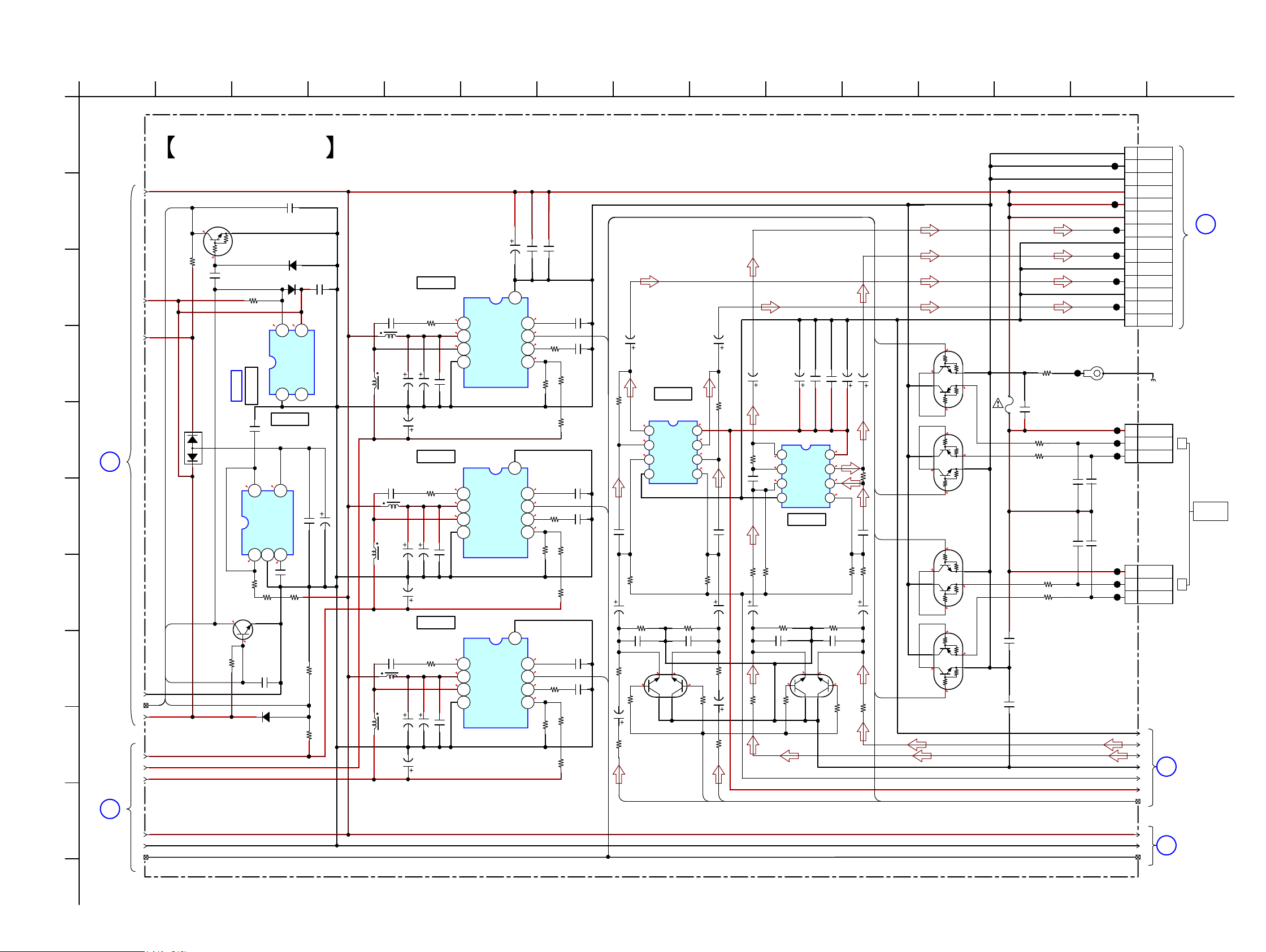
HCD-SH2000
5-11. SCHEMATIC DIAGRAM – MAIN BOARD (3/4) (Suffi x 11) –
1234567891011 141512 13
A
MAIN BOARD
14
12
C231
0.1
(3/4)
B
C
D
E
3.2
0
C232
0.47
R231 10k
10
9
RESET
IC B/D
MC2836-T112-1
D233
Q200
RESET
RT1N141C-TP-1
D231
D232
DA2J10100L
4.7kR232
3.4
1
IC101
OUT
S-80829CNNB-B8OT2G
VSS
IC101
0.1
IC102
+4V REG
IC102
TK11140CSCL-G
C241
3.4
DA2J10100L
C233
0.1
2
VDO
3NC4
C823
33uHL803
3
F
G
H
MAIN
BOARD
(1/4)
(Page 24)
19
AC-DET
11
13
12
92
I
17
20
19
4.0 13.5
13.5
R243
3.4
10k
R238
0
0
C240
5
VIN
ON/OFF2GND3NB
1
1.3
R242
0
Q203
AC-DET
0.1
4
VOUT
C239
0.1
R239
RT1N141M-TP-1
DA2J10100LD602
33uH
L804
C840
C833
L805
33uH
L808
33uH
C846
22
25V
16V
47
0.1
C238
C237
0
3.3k
R602
4.7k
R603
4
J
MAIN
BOARD
(Page 25)
(2/4)
18
16
15
• See page 54 for IC Block Diagrams.
16V
3300
0.1
C821
C820
IC800
0.1
L806
33uH
16V
47
C873
R842
C831
REGULATOR
IC800
BD9329AEFJ-E2
22
50V
16V100C 826
1000p
C800
22
25V
16.8
1
BST
13.5
2
VIN
12.5
3
SW
4
GND
COMP
9
2.6
8
SS
3.1
7
EN
2.0
6
0.8
5
FB
IC801
0.1
L807
33uH
16V47C874
REGULATOR
IC801
BD9329AEFJ-E2
R843
16V100C834
C839
22
25V
8.6
22
1
BST
13.5
2
VIN
4.0
3
50V1000pC801
SW
45
GND
COMP
9
2.6
SS
8
3.1
EN
7
1.5
6
0.6
FB
IC802
0.1
R844
16V
47
C875
REGULATOR
IC802
BD9329AEFJ-E2
22
50V
16V
100
1000p
C802
C841
0
BST
1
13.5
VIN
2
0
SW
3
GND
45
COMP
9
0
SS
8
0
EN
7
0
6
0
FB
10k
R802
10kR807
R810
10kR814
1000p
C803
R804
8.2k
0
R816
CN102
14P
14
CN705
3P
CN704
3P
13
12
11
10
9
8
7
6
5
4
3
2
1
1
2
3
1
2
3
GND
GND
GND
+13V
+13V
+13V
SW-L-CH
AGND
SW-R-CH
AGND
L-CH
AGND
R-CH
AGND
(CHASSIS)
13.5V
RED_LED
BLUE_LED
13.5V
RED_LED
BLUE_LED
23
24
25
26
27
28
29
30
31
32
6
7
G
DMB21
BOARD
(1/4)
CN1400
(Page 39)
L
SPEAKER
R
MAIN
BOARD
(4/4)
(Page 27)
MAIN
BOARD
(4/4)
(Page 27)
LED
JL519
JL520
JL521
JL522
JL523
JL100
ET800
JL524
E
JL401
JL402
JL403
C808
1000p
50V
C811
1000p
50V
JL404
JL405
JL406
C828
0.1
C829
1000p
50V
C836
C837
3300p
C843
0.1
25V
C844
2200p
50V
58
0.1
58
25
R801
22k
82k
R803
R806
7.5k
27kR808
R812
12k
47k
R815
0
4.7k
R794
22p
C774
100R782
16V10C7600R526
OUTL
50V
C767
C771
16V
R786
RT3CLLM
10
2.2k
R783
4.5
4.5
4.5
R795
Q600
MUTE
-3.0
47 k
C885
16V
10
IC600
OP-AMP
BA4558F
1
OUTPUT
2
INPUT-
3
INPUT+
4
GND
4.7k
470p
50V
0
600
IC
OUTPUT
R787
C768
VCC
INPUT-
INPUT+
0
R784
2.2k
R796
-3.0
C884
10
16V
4.7k
9
R797
8
4.5
7
4.5
6
4.5
5
47k
C772
16V
10
4.7k
470p
50V
R785
100
16V
10
C761
0R619
OUTR
MUTE
50V
22p
C776
16V
10
C887
0
R798
100
R788
C780
22p
50V
R799
4.7k
C777
16V
10
R792
C769
47k
R850
16V10C784
0.1C892
0.1C893
9
1
OUTPUT
4.5
4.5
2
INPUT-
4.5
3
INPUT+
4
GND
VCC
OUTPUT
INPUT-
INPUT+
8
4.5
7
4.5
6
4.5
5
IC805
OP-AMP
805
IC
BA4558F
C778
C770
16V
4.7kR793
470p
Q601
MUTE
0
RT3CLLM
-3.0
2.2k
R790
4.7k
470p
50V
0
-3.0
2.2k
R789
16V10C783
10
R791
52
16VC886 10
4.7k
R853
53
50V
22p
54
C782
0
R851 47k
R852
50V
55
100
0
Q604
0.6
0
0.8
0
RT3TAAM-TP-1
RT3TAAM-TP-1
RT3TAAM-TP-1
RT3TAAM-TP-1
0.5A
F700
50V
1000pC809
50V1000p
C804
0.8
0.6
0
0
3.2
Q605
0.8
Q606
0.9
0.8
Q607
0
0
Q607 - Q604
LED DRIVER
3.2
50V1000pC806
0R855
560R725
560R726
C807
1000p
50V
C810
1000p
50V
560R727
560R728
HCD-SH2000
2626
Page 27
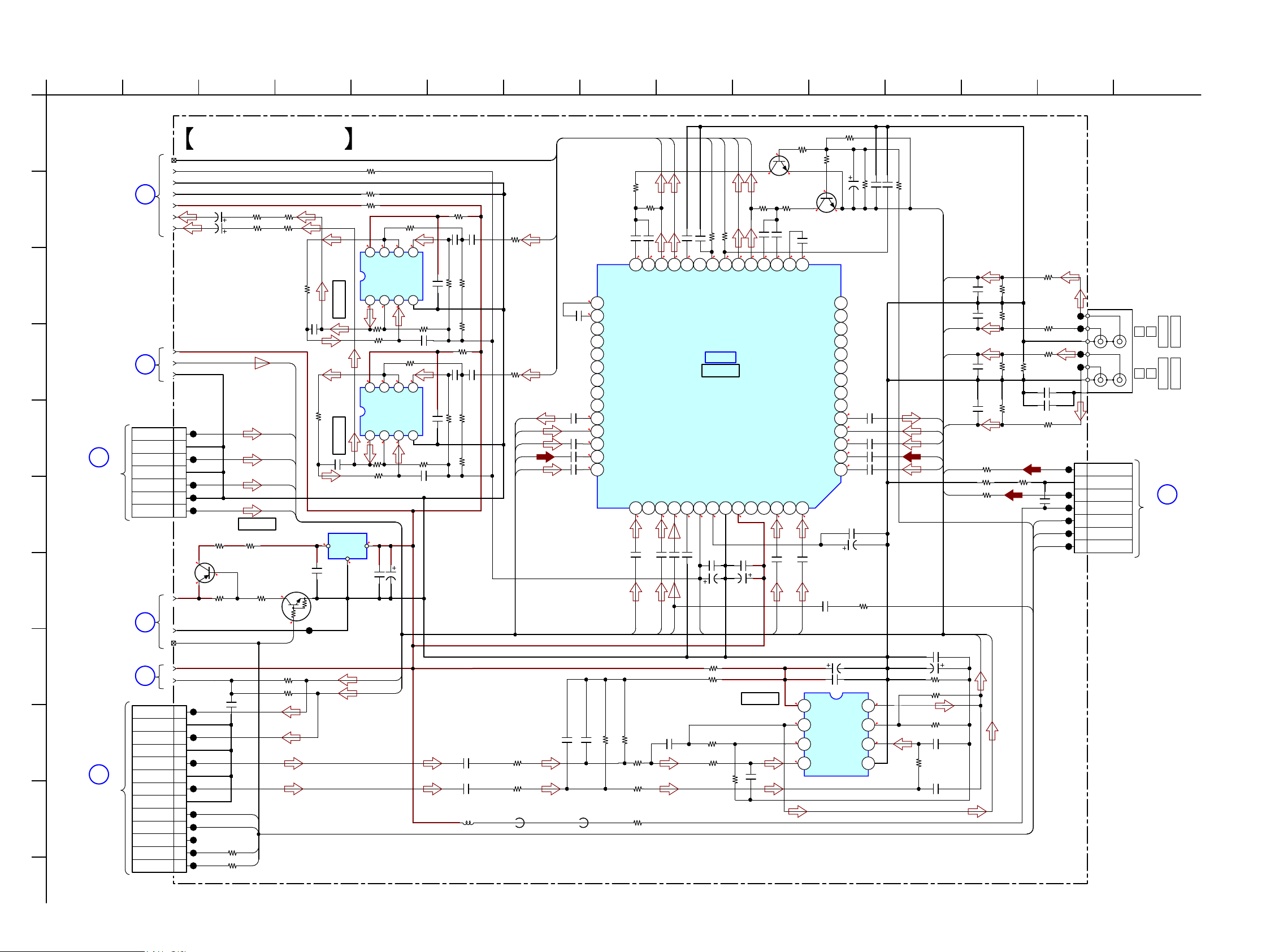
HCD-SH2000
5-12. SCHEMATIC DIAGRAM – MAIN BOARD (4/4) (Suffi x 11) –
1234567891011 141512 13
A
B
C
D
E
G
H
MAIN
BOARD
(3/4)
6
(Page 26)
MAIN
BOARD
(1/4)
2
(Page 24)
TV IN-L
A-GND
H
AUDIO-IN
BOARD
NO1200
(Page 51)
F
TV IN-R
A-GND
PC IN-R
A-GND
PC IN-L
MAIN
BOARD
(3/4)
7
(Page 26)
MAIN
BOARD
(2/4)
5
(Page 25)
RIN
AGND
I
I
DMB21
BOARD
(1/3)
J
CN4604
(Page 34)
LIN
AGND
LOUT
AGND(AVDD)
ROUT
AGND
/TAS_RESET
DATA_SEL
DGND
DSP-CLK
DSP-DATA
MAIN BOARD
29
27
26
23
28
24
25
3
1
2
CN106
7P
1
2
3
4
5
6
7
13.5
13.5
30
31
32
21
22
CN702
13P
13
12
11
10
9
8
7
6
5
4
3
2
1
16VC662 10
16VC661 10 0R6590R657
JL201
JL202
JL203
JL205
JL204
R817 0 R818 0
POWER SWITCH
Q800
2SB1690TL
12.8
R819 10k
POWER SWITCH
RT1N141C-TP-1
C812
0.1
JL743
JL741
JL739
JL773
JL735
JL734
JL744
JL732
JL731
0R745
0R744
IC803
R820
4.7k
Q801
79
38
78
77
0R658 0R662
MIC
TV IN-L
TV IN-R
PC IN-R
PC IN-L
IC803
+9V REG
KIA7809AF/API
0
3.1
58
47kR821
47kR822
C847
(4/4)
R857
R856
R854
BPF
IC503
C686
13.4
JL800
0.1
15k
R673
C659
IC502
I
IC503
BPF
IC502
0.1
COM
BA4558F
4.5
R690
R689 10k
4.5 4.5 4.5 9
BA4558F
4.5
R675
R674 10k
O
0
15k
R688
0.1
• See page 54 for IC Block Diagrams.
0
0
0
10R840
R692 10k
9 4.5 4.5 4.5
7
8
6
VCC
INPUT-
OUTPUT
OUTPUT
INPUT-
INPUT+
123
4.5
4.5
3.3k
R680 10k
7
8
6
VCC
INPUT-
OUTPUT
OUTPUT2INPUT-3INPUT+4GND
1
4.5
4.5
3.3k
9
16V100C825
0.1C813
INGAINOUTR
INGAINOUTL
5
INPUT+
GND
4
R691 10k
C691
5
INPUT+
R676
0.1
10k
0.1C674
0.1
C694
0.1
C676
0.1
C697
33k
R696 100k
R698
R697
10R839
0.1
C678
C680
100k
33k
R677
R679
C568 4.7
C570 4.7
C698
100k
0.22
R678
220uHL751
R848
0.22
R847
100k
0
AGCOUTR
0
AGCOUTL
INGAINOUTL
GAME_L
GAME IN-L
ST-L
DVD/SAT-L
C583
4.7
C540
4.7
C541
4.7
C542
4.7
C567
470p
3.3kR559
3.3kR560
600ohmFB750 600ohm
FB751
C629
C566
470p
4.7
4.5
29
4.5
30
31
32
33
34
35
36
37
4.5
38
4.5
39
4.5
40
4.5
41
4.5
42
R558 R557
10k 10k
47
OUTL
AGCOUTL
10kR528
R626
2.7k
0.1
0.1
C627
C528
4.5 4.5 4.5 4.5 4.5 0 0 4.5 4.5 4.5 4.5 4.5 4.5
VOLINL
TONEOUTL
BASS2L
BASS1L
MID2L
MID1L
TREL
RECBL
RECAL
INGAINOUTL
GAME_L
GAME IN-L
ST-L
DVD/SAT-L
R763 0
28
BB1L
43 44 45 46 47
4.7
C543
TV IN-L
R551
2.7k
R550
2.7k
TV IN-L
4.5
27
BB2L
NO_USE
OUTL
PC IN-L
4.5
4.7
C545
PC IN-L
2526
AGCOUTL
MIC
4.7
C546
MIC
820pC565
49
50VC522 220p
470
470R522
C524
1
AGCC
SWOUT
R521
CLK
DATA
IC B/D
IC500
IC500
SOUND CONTROL
R2A15216FP
GND
REFIN
REFOUT
VC
49 50 51 52 53 54 55 56
48
0.47
C648
0.1
C547
C548
100
16V
REFOUT
22R544
4.7k
R869
3.9kR548
2.7k
R549
R552
4.7k
VOLUME CONTROL
OUTR
AGCOUTR
2021222324
OUTR
AGCOUTR
DPLL/SURL
VCC
C551
0.1
C651
100
16V
IC501
IC501
BA4558F
Q528
2SC4154TP-1EF
0
4.6
R519
2.7k
0.1
C518
1819
BB1R
BB2R
PC IN-R
DPLR/SURR
4.7
C554
PC IN-R
LPF
C564
1000p
C617
4.6
R518
10k
0.1
1617
VOLINR
NO_USE
9
4.5
4.5
4.5
R628
47k
4.5
C615
4.7
15
TONEOUTR
BASS2R
BASS1R
INGAINOUTR
GAME_R
GAME IN-R
DVD/SAT-R
TV IN-R
4.54.594.54.54.54.5
4.7
C556
TV IN-R
C558
C559
8
VCC
7
OUT
6
-
5
+
R542
R620
47k
0
4.6
VOLUME CONTROL
2SC4154TP-1EF
MID2R
MID1R
TRER
SA2
SA1
RECBR
RECAR
ST-R
C549
4.7C509
1k
50V470pC513
C605
C503
C502
C501
-
+
50V
100kR543
C521 220p
R612 1M
4.7
4.7
4.7
4.7
0.1
16V100C649
100
16V47
4.5
1
4.5
2
4.5
3
4
REFOUT
INGAINOUTR
GAME_R
GAME IN-R
ST-R
DVD/SAT-R
R546
R547
2.7k
GAME IN-L
GAME IN-R
DVD/SAT-L
DVD/SAT-R
ST-L
ST-R
0.1C557
4.7kR870
3.9kR545
4.7k
C562
1000p
C561
820p
50V
6.3V47C894
C722
220p
C723
220p
C724
220p
C725
220p
R541
R841 0
R502
GAME_R
R741
R742
R748
R749
100
R751 0
100
DBFB
MIC-DATA-IN
GAME_L
27kR739
33k
R740
R743
R867
C726
C805
R747
1
JL600
27k
JL601
27k
0
24
22
20
JL602
JL603
0.47
1000p
27k
CN703
JL407
JL408
JL409
JL410
JL411
JL412
7P
7
6
5
4
3
2
1
REDRED
TUNER-L
AGND
TUNER-R
A+9V
TUNER_SDA
TUNER_SCK
TUNER_RDS
WHT
WHT
J500
LL
RR
TUNER
BOARD
CN1601
(Page 50)
AUDIO IN AUDIO IN
J
DVD/SAT GAME
33k
33k
33k
C754
16V
C620 10
Q518
14
13
12
11
10
9
8
7
6
4.5
5
4.5
4
4.5
3
4.5
2
4.5
1
R509
0.1
OUT
GND
HCD-SH2000
2727
Page 28

HCD-SH2000
Ver. 1.1
5-13. SCHEMATIC DIAGRAM – MAIN BOARD (1/4) (Suffi x 12) –
1234567891011 141512 13
A
MAIN BOARD
(1/4)
B
C
CN105
D
E
F
G
A
VOLUME
BOARD
CN1000
(Page 46)
AD-KEY-1
MASTER-VOL
LED-DRIVER-CLK
LED-DRIVER-LATCH
LED-DRIVER-OE
LED-DRIVER-DATA
MIC-GND
A+9V
MIC-SIGNAL
MIC-DET
STBY-LED
AD-KEY-0
SIRCS
D+3.3V
EVER+3.3V
/FL-DEIVER-CS
FL-DRIVER-DATA
FL-DRIVER-CLK
LED-GND
D-GND
LED+13.5V
23P
JL211
1
JL212
2
JL213
3
JL214
4
JL215
5
JL216
6
7
JL217
8
JL218
9
JL219
10
JL220
11
JL221
12
JL222
13
JL223
14
JL224
15
JL225
16
JL226
17
JL227
18
JL228
19
20
JL229
-VG
21
22
JL230
23
94
97
7
3
6
5
R186 10k
C298
RB185
0.1
R285 10k
100
*1 R190
*2 R290
C198
8282
93
84
85
80
86
89
87
68
88
4
89
21
92
1
2
94
9595
97
100100
H
C110
22p
I
J
MAIN
BOARD
(2/4)
(Page 29)
5
4
8
1
7
6
50V
• See page 53 for Waveforms. • See page 61 for IC Pin Function Descriptions.
IC100
C163
63
0.1
100R163
JL163
VSS
VCC2
PCONT-MAIN
VCC1
AC-CUT
NMI
TRG-SW
JL118
JL119
JL120
16VC216 100
47kR119
100R118
18
19
*1 R190
4.7K - SAF, EA
1k
- E2, E51, MX
*2 R290
330 - SAF
1k - EA
4.7k - E2, E51, MX
0 - MY
100R184
100R189
15kR294
470R194
0.1
10kR197
X110
32.768kHz
341
C111
22p
50V
C116
0.1
78
80
10kR180
1.5kR278
1.5kR277
JL180
0
JL181
81
1.3
JL182
JL183
JL184
JL185
JL186
JL187
JL188
JL189
JL190
JL191
JL192
JL193
JL194
JL195
JL197
JL200
2
R111
220k
R110
10M
3.2
3.2
0.4
2.8
1.4
3.4
3.4
3.4
3.2
1.3
USBA-LED-BLUE
82
0
83
TRYOPENPWM
84
CKSW
85
OCSW
86
0
REV
87
0
FWR
88
0
STBY-LED
89
DEST-IN
90
0
91
MTK-POWER-MONITOR
92
0
93
AD-KEY-1
94
0
USBB-LED-RED
95
0
Avss
96
MASTER-VOL
97
VREF
98
AVCC
99
100
50V100pC102
1
JL101
50VC100 100p
470R100
1
77
100R527
100R178
JL179
JL178
DSP-CLK
/DSP-RESET
MIC-DETECT
USBB-LED-BLUE
FL-DRIVER-CLK3LED-DRIVER-LATCH4SIRCS5LED-DRIVER-DATA
FL-DRIVER-DATA
2
2.7 3.2 3.2
JL102
JL103
JL104
470R102
100R103
3
2
4
75
10kR271
10kR272
10kR175
100R177
JL176
JL175
JL177
DSP-DATA
100R104
JL174
JL173
RESONANCE
/LED-DRIVER-OE
LED-DRIVER-CLK
BYTE9CNVss
6
7
8
3.2
0 0 0 0 0 0
JL105
JL106
JL107
100R107
100R105
5
7
6
707968
71
100R171
JL171
/SD-SLOW
69
C162
100
16V
100R170
JL170
/DAMP-RESET
15kR274
470R174
0.47
C165
JL169
JL168
JL167
3.3 03.4 3.4 0 3.23.23.23.23.2 3.02.9 3.2 0.8
NO USE
AD-KEY-0
MIC-DATA-IN
72
100
R172
JL172
/SD-FAST
IC100
SYSTEM CONTROL
R5F3650KBDFA
1 2
Xcin
Xcout
RESET
X-OUT
VSS
R213
X113
8MHz
X-IN
1MR113
0
C115
22p
50V
10 11 12 13 14 15 16 17 18 19 20 21 22 23 24 25 26 27 28 29 30
2.9
1.2 3.2 1.7 1.6 3.2 3.2 3.2 3.1 3.3 3.3 3.3 1.6 0.6 3.3 3.4 3.43.10
1.1
150k
R109
JL112
C113
27p
50V
61
100R161
JL161
/FAN-LOCK
ST-RDS
100
R120
20
59
60
100R159
100R160
JL159
JL160
FAN- EN
/FL-DRIVER-CS
JL121
JL122
220R121
100
R122
R222
21
22
PCONT-SUB
ST-CLK
4.7k
58
100R158
JL158
JL123
SUB-ON
JL124
R224
4.7k
24
10kR261
JL157
ST-DATA
100R124
JL156
VBUS-OE
JL125
100R125
54
55
JL155
JL154
SPK-R-LED-RED
SPK-R-LED-BLUE
/HUB-OC1
DAMP-CLK
JL126
JL127
100R126
100R229
R225 100k
25
27
52
53
JL153
JL152
SPK-L-LED-RED
SPK-L-LED-BLUE
MTK-POWER-CTL
/HUB-OC2
I2C-CLK
JL128
JL129
100R230
10kR129
28
51
D167
MC2840-T112-1
JL151
3.200000 3.2 3.1 3.2 3.4 0 1.6 3.4 3.20
515253545556575859606162636465666768697071727374757677787980
/LINE-MUTE
AUDIO-CLK
AUDIO-DATA
FLASH-MEMORY
HUB-VBUS-DET
HUB-RESET
MTK-RESET
MTK-XIFCS
MTK-BUSY
CLK-OUT
DIGITAL-SEL
MTK-CLK
MTK-SIO
MTK-SOD
RTS1
CLK1
RXD1
TXD1
I2C-DATA
JL130
10kR130
0R226
26
0.1C127
0.1C128
2
3
MAIN
BOARD
(4/4)
(Page 31)
B
DAMP
BOARD
(1/4)
CN1401
(Page 39)
MAIN
BOARD
(3/4)
(Page 30)
2
3
1
MIC-DATA-IN
CN100
JL512
JL511
JL510
JL508
JL507
JL506
JL505
JL513
JL504
JL503
JL502
JL501
JL500
13.4
LED SWITCH
Q205
2SB1690TL
13.4
14P
14
13
12
11
10
9
8
7
6
5
4
3
2
1
PCONT (SUB)
PCONT (MAIN)
AC-DET
/SD-FAST
DBFB
FAN-EN
FAN-LOCK
DGND
DAMP-CLK
/S D - S L O W
NO USE
/DAMP-RESET
RESONANCE
NC
9
11
10
14
12
13
59
63
AC-DET
7272
R258
4.7k
DBFB
60
61
26
49
71
69
4747
70
75
4545
44
43
42
41
40
38
37
36
35
R259
10k
12.7
2.2C267
0
JL150
50
0
JL149
49
0
R241
JL148
48
47
46
45
44
43
42
41
40
39
38
37
36
35
34
33
32
31
10k
0
JL147
0
JL146
3.2
JL145
3.2
3.2
JL143
3.0
JL142
2.4
JL141
2.4
JL140
0
JL139
3.2
JL138
3.1
JL137
0.1
JL136
0.4
JL135
1.3
JL134
1.3
JL133
1.3
JL132
3.2
JL131
DA2J10100LD267
100kR167
10kR146
RB140
100
R138
100
R137
100
100
R136
100
R135
RB131
100
POWER SWITCHING
Q204
RT1N141C-TP-1
0
58
3.10
HCD-SH2000
2828
Page 29

HCD-SH2000
5-14. SCHEMATIC DIAGRAM – MAIN BOARD (2/4) (Suffi x 12) –
1234567891011 141512 13
A
B
MAIN
BOARD
(1/4)
(Page 28)
1
MAIN BOARD
5
8
7
4
6
82
C
Q301
LED DRIVE
RT3NDDM-T111-1
D
CN300
14P
JL361
1
JL362
3
JL363
4
JL364
5
JL365
FB300
FB302
0
0
C345
C346
0.1
18
84
85
86
87
88
37
36
35
42
40
41
6
JL366
D-A
7
JL367
8
9
10
JL310
11
JL311
D-B
12
JL312
13
14
15
ET300
E
CN700
13P
JL711
13
JL710
12
JL709
11
JL708
10
JL707
9
JL706
8
JL705
7
JL712
6
JL704
5
JL703
4
JL702
3
JL701
2
JL700
1
0.1
C347
0.1
C344 0.1
Q303
LED DRIVE
RT1N141C-TP-1
MC2840-T112-1
C707
6.9 0
D704
E
F
G
H
J
LED13.5V
USBA-LED-BLUE
USBB-LED-RED
USBB-LED-BLUE
USB A+5V
USB
BOARD
NO1152
C
(Page 48)
I
DMB21
BOARD
(2/3)
CN109
(Page 35)
D
D+A
USB A GND
SHIELD
USB B+5V
D+B
USB B GND
SHIELD
(CHASSIS)
TRG-SW
TROPENPWM
CKSW
OCSW
REV
FWD
IFSCK
DGND
IFSOD
IFSDI
XSYSRST
XIBSY
XIFCS
• See page 53 for Waveforms. • See page 54 for IC Block Diagrams.
(2/4)
95
100
1.3
D-A
D+A
D-B
D+B
0.1
D+A
D+B
27
C339
0.1
0.1
+IN2
OUT2
VCC
16V10
0
5
0
-IN2
6
3.3
7
9.0
8
100R340
C340
R342
330
C337
C338
0
4
GND
0.1
R338
C342
0
3
22k
0.1
+IN1
0
2
-IN1
0
1
OUT1
IC B/D
R344
0.1
C335
10
C435
0.1
C305
C310
C415
0
1
0
2
0
3
0
4
3.3
5
0.1
0.1
0.1
6
7
8
9
D-A
D-B
IC301
IC301
USB COMPARATOR
NJM2903V(TE2)
C332
22p
12kR335
0.1
C336
USBDN1_DM
USBDN1_DP
USBDN2_DM
USBDN2_DP
VDDA33
NC
NC
NC
NC
3.3 0 3.3 3.3
50V
RBIAS
VDD33PLL
VDD18PLL
IC300
IC300
USB CONTROLER
USB2512B-AEZG
VDDA33
PRTPWR1
TEST
101112 13 14 15 16 17
C311
C411
0
R333
XTAL2
XTAL1/CLKIN
3
VDD18
OCS1_N
10
0.1
28
100R339
22kR337
330
R341
C341
0.1
R343
0.1
0R331
0R330
100kR328
28
2930313233343536
VDDA33
USBUP_DP
USBUP_DM
NON_REM0
VBUS_DET
HS_IND/CFG_SEL1
SCL/SMBCLK/CFG_SEL0
SDA/SMBDATA/NON_REM1
OCS2_N
PRTPWR2
VDD33CR
NC
18
R332
1M
X332
0.1C328
24MHz
03.303.01.61.301.23.3
SUSP_IND/
LOCAL_PWR/
RESET_N
VDD33
NC
NC
NC
10kR127
10kR128
R426
100k
3.2
27
3.2
26
0
25
0.3
24
3.3
23
0.4
22
21
20
19
JL327
JL326
C334
10p
50V
C426
C326
100kR325
100kR324
0.1C323
100kR322
10C321
15
16
17
18
19
MAIN
BOARD
4
(3/4)
(Page 30)
20
470kR263
MUTE
2.2C250
47kR262
51
Q207
MUTING
RT1P141C-TP-1
2.2kR264
(CHASSIS)
ET302
JL351
JL350
E
CN302
3P
SHIELD
1
USBP
2
USBM
3
DMB21
BOARD
E
(2/3)
CN1108
-3.0
3.2
3.3
(Page 35)
IC804
IC804
+5V REG
BD00GC0WEFJ-E2
43
R823
0.1
C748
10k
R824
27k
R825
27k
R826
100k
R827
100k
0.1
C327
10
0.1
R327 220
R326 220
45
44
16V
10
C850
3.1
4
0
3
0.8
2
5.1
1
0.1
C851
3.1
R830 1.2k
0
0
R834 470
POWER CONTROL
SWITCH
Q803
RT3N77M-TP-1
NC
GND
FB
VO
R835
10k
POWER CONTROL
EN
NC
NC
VCC
9
R831 10k
2.6
DRIVER
Q805
2SB1690TL
3.1
5
6
7
9.0
8
C852
100
16V
R828
0
9.0
9.0
POWER CONTROL
DRIVER
Q804
2SB1690TL
JL720
JL724
JL721
JL725
JL722
JL726
JL723
8.3
3.3
3.2
CN701
7P
7
6
5
4
3
2
1
22
21
VM (9V)
MGND
DVDD3.3V
DGND
DVDD5V
AGND
AVDD5V
5
MAIN
BOARD
(4/4)
(Page 31)
F
DMB21
BOARD
(1/3)
CN602
(Page 34)
HCD-SH2000
2929
Page 30

HCD-SH2000
5-15. SCHEMATIC DIAGRAM – MAIN BOARD (3/4) (Suffi x 12) –
1234567891011 141512 13
A
14
B
10
MAIN BOARD
12
3.2
0
C232
0.47
R231 10k
C231
Q200
RESET
RT1N141C-TP-1
D231
D232
DA2J10100L
4.7kR232
0.1
DA2J10100L
C233
(3/4)
0.1
C
3.4
3.4
1
0.1
C238
4
VOUT
0.1
C241
VSS
OUT
3NC4
C237
16V
2
47
VDO
4.0
5
VOUT
RESET
IC B/D
IC101
TYPE B
IC103
+4V REG
IC103
XC6216B402MR
4
13.5
CE
IC101
S-80829CNNB-B8OT2G
C242
0.1
D
E
3
MAIN
BOARD
(1/4)
9
TYPE A
MC2836-T112-1
IC102
D233
+4V REG
IC102
TK11140CSCL-G
4.0
5
13.5
VIN
(Page 28)
F
G
H
ON/OFF2GND3NB
1
1.3
13.5
19
AC-DET
11
13
12
I
17
20
19
92
3.4
0
10k
C240
R238
Q203
AC-DET
0.1
C239
0.1
RT1N141M-TP-1
DA2J10100LD602
VIN2VSS3NC
1
13.5
3.3k
R602
4.7k
R603
4
MAIN
BOARD
J
(Page 29)
(2/4)
18
16
15
• See page 54 for IC Block Diagrams.
16V
3300
0.1
C821
C820
IC800
33uHL803
C823
0.1
L806
33uH
16V
47
C873
R842
C831
REGULATOR
IC800
BD9329AEFJ-E2
22
50V
16V100C 826
1000p
C800
22
25V
16.8
1
BST
13.5
2
VIN
12.5
3
SW
4
GND
COMP
9
8
SS
7
EN
6
5
FB
IC801
33uH
L804
C833
0.1
L807
33uH
16V47C874
REGULATOR
IC801
BD9329AEFJ-E2
R843
16V100C834
C839
22
25V
8.6
22
1
BST
13.5
2
VIN
4.0
3
50V1000pC801
SW
45
GND
COMP
9
SS
8
EN
7
6
FB
IC802
C840
L805
33uH
L808
33uH
C846
25V
REGULATOR
IC802
BD9329AEFJ-E2
0.1
R844
16V
47
C875
22
16V
100
C841
0
22
50V
1000p
C802
BST
1
13.5
VIN
2
0
SW
3
GND
45
COMP
9
SS
8
EN
7
6
FB
14
C808
1000p
50V
C811
1000p
50V
JL404
JL405
JL406
CN102
14P
CN705
3P
CN704
GND
13
GND
12
GND
11
+13V
10
+13V
9
+13V
8
SW-L-CH
7
AGND
6
SW-R-CH
5
AGND
4
L-CH
3
AGND
2
R-CH
1
AGND
(CHASSIS)
13.5V
1
RED_LED
2
BLUE_LED
3
3P
1
13.5V
2
RED_LED
3
BLUE_LED
23
24
25
26
6
27
28
29
30
31
7
32
G
DMB21
BOARD
(1/4)
CN1400
(Page 39)
L
SPEAKER
R
MAIN
BOARD
(4/4)
(Page 31)
MAIN
BOARD
(4/4)
(Page 31)
LED
JL519
JL520
JL521
1000p
JL522
C803
C828
10k
R802
10kR807
R810
10kR814
R804
8.2k
0
R816
0.1
C829
1000p
50V
C836
C837
3300p
C843
25V
C844
2200p
50V
58
0.1
58
0.1
25
R801
22k
82k
R803
R806
7.5k
27kR808
R812
12k
47k
R815
0
4.7k
R794
50V
22p
C774
100R782
16V10C7600R526
OUTL
C771
R786
C767
C885
16V
4.5
4.5
4.5
R795
47 k
16V
10
Q600
MUTE
RT3CLLM
-3.0
2.2k
R783
10
470p
1
2
3
4
OUTPUT
INPUT-
INPUT+
GND
4.7k
50V
0
IC600
OP-AMP
BA4558F
600
IC
R787
C768
VCC
OUTPUT
INPUT-
INPUT+
0
R784
2.2k
R796
-3.0
47k
470p
C884
10
16V
4.7k
9
R797
8
4.5
7
4.5
6
4.5
5
C772
16V
10
4.7k
50V
R785
100
16V
10
C761
0R619
OUTR
MUTE
50V
22p
C776
16V
10
C887
C780
0
R798
100
R788
22p
50V
R799
4.7k
C777
16V
10
R792
C769
47k
R850
16V10C784
0.1C893
0.1C892
9
1
OUTPUT
4.5
4.5
2
INPUT-
4.5
3
INPUT+
4
GND
VCC
OUTPUT
INPUT-
INPUT+
8
4.5
7
4.5
6
4.5
5
IC805
OP-AMP
805
IC
BA4558F
C778
C770
16V
4.7kR793
470p
Q601
MUTE
0
RT3CLLM
-3.0
2.2k
R790
4.7k
470p
50V
0
-3.0
2.2k
R789
16V10C783
10
R791
52
16VC886 10
4.7k
R853
53
50V
22p
54
C782
R851 47k
R852 0
50V
55
100
0
Q604
0.6
0
0.8
0
RT3TAAM-TP-1
50V1000pC806
RT3TAAM-TP-1
RT3TAAM-TP-1
RT3TAAM-TP-1
0.5A
F700
50V
1000pC809
50V1000p
C804
0.8
0.6
0
0
3.2
Q605
0.8
Q606
0.9
0.8
Q607
0
0
Q607 - Q604
LED DRIVER
3.2
2.6
3.1
2.0
0.8
2.6
3.1
1.5
0.6
0
0
0
0
R855
0
C807
1000p
C810
1000p
50V
JL523
JL524
JL100
E
ET800
JL401
JL402
560R725
JL403
560R726
50V
560R727
560R728
HCD-SH2000
Note 1: Refer to the servicing notes “MAIN BOARD
DISCRIMINATION” (page 5) for how to distinguish
SUFFIX-11 and SUFFIX-12.
Note 2: A part of circuit composition of MAIN board (Suffi x-12) has been changed in the
midway of production. MAIN board (Suffi x-12) that has not been changed appears
as TYPE A, and the changed MAIN board (Suffi x-12) appears as TYPE B.
3030
Note 3: IC103 and C242 (Combination: TYPE B) on the MAIN board (Suffi x-12) cannot exchange
with single. When these parts on the MAIN board (Suffi x-12) are damaged, remove IC103
and C242 (Combination: TYPE B) and replace with IC102 and C239 (Combination: TYPE A).
Page 31

HCD-SH2000
5-16. SCHEMATIC DIAGRAM – MAIN BOARD (4/4) (Suffi x 12) –
1234567891011 141512 13
A
B
C
D
E
F
G
H
MAIN
BOARD
(3/4)
6
(Page 30)
MAIN
BOARD
(1/4)
2
(Page 28)
TV IN-L
A-GND
H
AUDIO-IN
BOARD
NO1200
(Page 51)
TV IN-R
A-GND
PC IN-R
A-GND
PC IN-L
MAIN
BOARD
(3/4)
7
(Page 30)
MAIN
BOARD
(2/4)
5
(Page 29)
RIN
AGND
I
I
DMB21
BOARD
(1/3)
J
CN4604
(Page 34)
LIN
AGND
LOUT
AGND(AVDD)
ROUT
AGND
/TAS_RESET
DATA_SEL
DGND
DSP-CLK
DSP-DATA
MAIN BOARD
29
27
26
23
28
24
25
3
1
2
CN106
7P
1
2
3
4
5
6
7
13.5
13.5
30
31
32
21
22
CN702
13P
13
12
11
10
9
8
7
6
5
4
3
2
1
16VC662 10
16VC661 10 0R6590R657
JL201
JL202
JL203
JL205
JL204
R817 0 R818 0
POWER SWITCH
Q800
2SB1690TL
12.8
R819 10k
POWER SWITCH
RT1N141C-TP-1
C812
0.1
JL743
JL741
JL739
JL773
JL735
JL734
JL744
JL732
JL731
0R745
0R744
IC803
R820
4.7k
Q801
79
38
78
77
0R658 0R662
MIC
TV IN-L
TV IN-R
PC IN-R
PC IN-L
IC803
+9V REG
KIA7809AF/API
0
3.1
58
47kR821
47kR822
C847
(4/4)
R857
R856
R854
9 4.5 4.5 4.5
BPF
IC503
C686
13.4
JL800
0.1
15k
R673
C659
I
IC503
BPF
IC502
IC502
0.1
COM
BA4558F
4.5
R690
R689 10k
4.5 4.5 4.5 9
BA4558F
4.5
R675
R674 10k
O
0
15k
R688
0.1
• See page 54 for IC Block Diagrams.
0
0
0
10R840
R692 10k
7
8
6
VCC
INPUT-
OUTPUT
OUTPUT
INPUT-
INPUT+
234
1
4.5
4.5
3.3k
R680 10k
7
8
6
VCC
INPUT-
OUTPUT
OUTPUT2INPUT-3INPUT+4GND
1
4.5
4.5
3.3k
9
16V100C825
0.1C813
INGAINOUTR
INGAINOUTL
5
INPUT+
GND
R691 10k
C691
5
INPUT+
R676
0.1
10k
0.1C674
0.1
C694
0.1
C676
0.1
C697
33k
R696 100k
R698
10R839
0.1
C678
100k
33k
R677
R679
C568 4.7
C570 4.7
C698
R697
C680
100k
R678
220uHL751
R848
0
0.22
R847
0
0.22
100k
FB750 600ohmFB751
AGCOUTR
AGCOUTL
INGAINOUTL
GAME_L
GAME IN-L
ST-L
DVD/SAT-L
3.3kR559
3.3kR560
600ohm
C567
470p
C583
4.7
C540
4.7
C541
4.7
C542
4.7
C629
C566
470p
4.7
4.5
29
4.5
30
31
32
33
34
35
36
37
4.5
38
4.5
39
4.5
40
4.5
41
4.5
42
R558 R557
10k 10k
47
OUTL
AGCOUTL
10k
R626
2.7k
R528
0.1
0.1
C627
C528
4.5 4.5 4.5 4.5 4.5 0 0 4.5 4.5 4.5 4.5 4.5 4.5
VOLINL
TONEOUTL
BASS2L
BASS1L
MID2L
MID1L
TREL
RECBL
RECAL
INGAINOUTL
GAME_L
GAME IN-L
ST-L
DVD/SAT-L
R763 0
28
BB1L
TV IN-L
43 44 45 46 47
4.7
C543
TV IN-L
R551
2.7k
R550
2.7k
2526
27
BB2L
OUTL
AGCOUTL
MIC
PC IN-L
NO_USE
4.5
4.5
4.7
4.7
C545
C546
MIC
PC IN-L
820pC565
49
50VC522 220p
470
470R522
C524
1
AGCC
SWOUT
R521
222324
CLK
DATA
IC B/D
IC500
IC500
SOUND CONTROL
R2A15216FP
GND
REFOUT
REFIN
VC
49 50 51 52 53 54 55 56
48
0.47
C648
0.1
C547
C548
100
16V
REFOUT
22R544
4.7k
R869
3.9kR548
2.7k
R549
R552
4.7k
2021
VOLUME CONTROL
2SC4154TP-1EF
OUTR
AGCOUTR
OUTR
AGCOUTR
DPLL/SURL
VCC
C551
0.1
C651
100
16V
IC501
IC501
LPF
BA4558F
1000p
4.6
R519
2.7k
0.1
C518
1819
BB2R
DPLR/SURR
C564
Q528
0
BB1R
PC IN-R
4.7
C554
PC IN-R
C617
4.6
R518
10k
0.1
1617
4.5
4.5
4.5
15
VOLINR
NO_USE
4.7
TV IN-R
9
R628
47k
0
4.5
C615
4.7
TONEOUTR
BASS2R
BASS1R
MID2R
MID1R
TRER
RECBR
RECAR
INGAINOUTR
GAME_R
GAME IN-R
ST-R
DVD/SAT-R
TV IN-R
4.54.594.54.54.54.5
C556
C558
C559
8
VCC
7
OUT
6
-
5
+
R542
R620
47k
16VC620 10
4.6
VOLUME CONTROL
Q518
2SC4154TP-1EF
14
13
12
11
10
SA2
9
SA1
8
7
6
4.5
5
4.5
4
4.5
3
4.5
2
4.5
1
C549
4.7C509
R509
0.1
OUT
GND
C605
C503
C502
C501
-
+
1k
50V470pC513
50VC521 220p
100kR543
R612 1M
4.7
4.7
4.7
4.7
0.1
16V100C649
100
16V47
4.5
1
4.5
2
4.5
3
4
REFOUT
INGAINOUTR
GAME_R
GAME IN-R
ST-R
DVD/SAT-R
R546
R547
2.7k
GAME IN-L
GAME IN-R
DVD/SAT-L
DVD/SAT-R
ST-L
ST-R
0.1C557
4.7kR870
3.9kR545
4.7k
C562
1000p
C561
820p
50V
6.3V47C894
C722
220p
C723
220p
C724
220p
C725
220p
R541
R841 0
R502
GAME_R
R741
R742
33k
R748
R749
33k
100
R751 0
100
DBFB
MIC-DATA-IN
GAME_L
27kR739
33k
JL600
R740
27k
JL601
R743
27k
R867
33k
0
C726
C805
R747
C754
1
JL602
JL603
0.47
1000p
27k
CN703
JL407
JL408
JL409
24
JL410
22
JL411
20
JL412
7P
7
6
5
4
3
2
1
REDRED
TUNER-L
AGND
TUNER-R
A+9V
TUNER_SDA
TUNER_SCK
TUNER_RDS
WHT
WHT
J500
LL
RR
TUNER
BOARD
CN1601
(Page 50)
AUDIO IN AUDIO IN
J
DVD/SAT GAME
HCD-SH2000
3131
Page 32

HCD-SH2000
5-17. PRINTED WIRING BOARDS – DMB21 BOARD (Component Side) –
1234567891011 141512 13
A
DMB21 BOARD (Component side)
B
C
D
E
F
G
H
(CHASSIS)
MAIN
BOARD
CN702
(Page 20) (Suffix 11)
(Page 22) (Suffix 12)
MAIN
BOARD
CN701
F
(Page 20) (Suffix 11)
(Page 22) (Suffix 12)
I
(CHASSIS)
ET004
D004
C623
C4631
R521
R4847
C4608
R4835
JL010
JL012
13
I
CN4604
JL021
JL022
JL002
1
JL023
C4632
R4841
R4843
JL019
C4634
IC4609
C4638
R4848
C4633
JL014
JL016
JL024
C4636
JL017
C604
17
C608
C607
CN602
JL006
C601
JL007
R608
D003
C622
ET003
• See page 14 for Circuit Boards Location.
JL1216
IC4608
R4845
R4846
R4861
C4650
IC4605
R4850
R4873
C4639
JL001
JL003
JL005
C4637
R4879
X002
R4842
C4635
C4644
R4853
C4641
C4640
C602
C603
R4856
CL4001
CL4005
R4878
R4857
R4854
R4867
R4855
JL201
CL4003
R4877
CL4004
CL4002
R4852
R4862
JL202
C217
CL208
R247
C185
JL004
R232
R231
CN201
CL207
CL206
R230
JL1214
R1248
CL1141
JL115
C189
C220
JL205
CL1142
CL1146
JL1218
R1276
C218
R1283
JL206
• : Uses unleaded solder.
CL1151
JL1220
R1281
R1269
JL113
R1277
R246
R1282
CL213
JL114
CL1140
JL203
JL210
CL1147
C216
JL214
CL1150
CL1139
CL1148
CL106
JL213
C190
R1249
CL1149
C1504
C112
CL107
7
RB114 RB115
C124
R107
JL212
CN202
CL1152
RB111
CL1138
R142
R1168
X101
C152 C153
JL111 6
JL1120
C105
1
NC
CN105
RB113
RB112
IC101
JL111 4
JL1101
C106
C113
R114
JL1105
JL1102
IC104
FB111 4
R1121
C118
JL1107
JL1106
JL1123
C620
CL105
C160
R156
JL1131
JL1132
JL1133
JL1134
JL111 7
FB1265
JL1209
JL111 5
JL111 8
JL1122
R1151
JL1203
JL1208
D001
JL1204
JL1206
JL1207
R1152
JL1213
JL111 9
JL1201
JL1212
C621
RB105
RB106
JL1202
JL1205
JL1211
12
R1110
RB108
RB107
R1263
CL109
CL108
FB1266
FB1264
R1123
C156
R103
JL111 3
R102
C101
JL1111
CN101
JL111 0
JL111 2
JL1108
ET002
1
13
JL1210
CN1108
D002
JL1121
ET001
1-883-583-
CN109
(CHASSIS)
D
(Page 20) (Suffix 11)
(Page 22) (Suffix 12)
E
(Page 20) (Suffix 11)
(Page 22) (Suffix 12)
12
(12)
(CHASSIS)
MAIN
BOARD
CN700
MAIN
BOARD
CN302
J
HCD-SH2000
DEVICE, OPTICAL
KHM-313CAB/C2RPA
MS-214
BOARD
DEVICE, OPTICAL
KHM-313CAB/C2RP
Note 1: IC4605 on the DMB21 board cannot exchange with
single. When this part on the DMB21 board is damaged,
exchange the entire mounted board.
Note 2: When the MS-214 board is defective,
exchange the entire MD (AU) ASSY.
3232
Page 33

HCD-SH2000
5-18. PRINTED WIRING BOARDS – DMB21 BOARD (Conductor Side) –
1 2 3 4 5 6 7 8 9 10 11 14 1512 13
A
DMB21 BOARD (Conductor side)
B
C
D
E
F
G
H
I
• See page 14 for Circuit Boards Location.
C144
R117
Q101
R122
C175
C151
C197
C1505
FB108
C172
C149
C111
C115
R136
C116
R1184
R109
R1129
G1 D2S1
Q103
D1 G2 S2
C1507
C179
C180
IC102
R1192
C191
FB1267
FB1268
R1252
C1513
C102
R125
C1512
C181
C150
R1177
R1193
R1191
R1194
R108
R116
R111
R1150
C119
R115
C127
R1255
R110
Q102
R113
R2502
C168
• : Uses unleaded solder.
R1280
IC4607
R4844
FB607
C4629
R4840
R604
C4626
D005
C4602
C4603
C4606
R4876
R4602
R4872
R630
R4608
R4838
IC4601
R4837
R601
R4606
R4601
R4611
R4609
R4849
R4834
C4622
R4833
8
1
C4645
FL603
IO
R605
FB603
C4623
R611
C611
12
1-883-583-
(12)
R4874
C4628
R214
1
R206
48
37
C205
R208
C221
C198
CL201
R212
R226
C214
R233
C215
R4851
R223
R225
C212
C209
R234
R221
R4858
C211
R220
C4642
C4643
C233
R4839
R4859
R4871
R4870
IC4602
9
16
R606
R612
R1213
IO
FL105
R1105
R154
C146
C125
R155
C169
C155
R2507
R1101
C154
C213
C108
C145
C199
C1506
CL205
R133
C210
C126
R1262
R1261
R1250
R210
R219
R254
R227
R228
R224
R213
R101
CL204
13
C208
R216
12
IC111
R1278
R205
R204
C203
R1279
R207
C183
C192
R1290
CL202
R1178
C193
R1256
C188
IC107
C195
R2506
R209
C206
R215
IC201
R118
R120
R121
R123
R256
24
E1B1B2E2C2
C1
R124
R237
C226
R2505
R255
R112
C225
25 36
C223
R236
R239
R238
C222
C219
C224
J
HCD-SH2000
Note: IC102 on the DMB21 board cannot exchange with
single. When this part on the DMB21 board is
damaged, exchange the entire mounted board.
3333
Page 34

HCD-SH2000
5-19. SCHEMATIC DIAGRAM – DMB21 BOARD (1/3) –
1234567891011 141512 13
A
B
BOARD
CN701
(Page 25) (Suffix 11)
(Page 29) (Suffix 12)
C
D
E
F
MAIN
(2/4)
DMB21
BOARD
(3/3)
(Page 36)
DMB21
BOARD
(2/3)
(Page 35)
AVDD5V
AGND
DVDD5V
DGND
DVDD3.3V
MGND
VM (9V)
VM9V
MTR_GND
DVDD5V
8
DGND
DVDD3.3V
DGND
ACLK
ALRCK
ABCK
9
ADIN
ASDATA0
DMB21 BOARD
CN602
7P
JL001
1
JL002
2
JL003
3
JL004
4
5
6
7
47
R4841
100
10k
R4843
R4872
JL005
JL006
JL007
0
3.1
JL019
FB603 220ohm
IC4609
1
CK
2
D
3
_Q
4
GND
D TYPE FLIP FLOP
TC7WH74FK
VCC
_PR
_CLR
000
R604 R612
000
FL603
R608
IC4609
3.1
8
3.1
7
3.1
6
3.1
5
Q
F
G
H
IC B/D
IC4607
IC4607
ASYNCHRONOUS SAMPLE
RATE CONVERTER
SRC4182
C4629 0.10.01C4630
I
R4844 100
J
DATA-SEL
• See page 53 for Waveforms. • See page 54 for IC Block Diagrams.
(1/3)
R611 R601
0
R4839
R4847
0.1
C4632
100
0
G
EMI
1
0
2
0
3
4
0
1
1.5
2
3
1.1
4
1.7
5
1.7
6
2.9
7
0
8
9
10
11
12
3.2
13
0
R605
R606
FB607 220ohm
IC4608
MULTIPLEXER
TC7WH157FK
A
B
_Y
GND
LGAP
RCKI
NC
SDIN
BCKI
LRCKI
VIO
DGND
BYPAS
IFMT0
IFMT1
IFMT2
_RST
MUTE
R4874
VCC
MODE2
MODE1
MODE0
BCKO
LRCKO
SDOUT
DGND
TDMI
OFMT0
OFMT1
OWL0
OWL1
_RDY
0
10V100C602
10V100C603
C611 0.1
IC B/D
3.1
8
C4631
0.1
7
_ST
3.1
6
SEL
0
5
Y
R4845
100
28
27
26
25
24
23
VDD
22
21
20
19
18
17
16
1514
47
0
R4842
R4876
1.5
1.5
R4851
100
1.1
2.9
C4628
0.1
0
IC4608
C4633
10
16V
7
X002
12.288MHz
C4635
R4871
R4856
10k
R4857
10k
R4852
100
16VC4634 10
0
C4636 0.1
R4849
0.01C4638
27pC4639
33pC4640
R4873
0
R4850
0
0.1
R4879
CL4001
10k
10p
10p
CL4002
C4642
C4643
CL4003
CL4004
R4877
47
47
R4870
100
DATA
CLK
IC4605
IC4605
DSP
TAS3108DCPR
1
AVSS
1.8
2
VR_PLL
0.9
3
XTALI
0.8
4
XTALO
0
5
MCLKI
6
MCRCK_DVR
7
CS0
0
8
GPIO
3.1
9
DVDD
10
DVSS
0
11
SDIN1
12
SDIN2
13
SDIN3
14
SDIN4
3
15
SDA1
3.0
16
SCL1
3.1
17
SDA2
3.1
18
SCL2
0.1
19
LRCK
AVDD
RSRV
PLL2
PLL1
PLL0
SRV
_RESET
_PDN
DVDD
DVSS
VR_DIG
SDOUT1
SDOUT2
SDOUT3
SDOUT4
SCLKOUT2
SCLKOUT1
MCLKO
SCLKIN
R4837
0
2.6
2.6
2.9
0
0
1.1
9
1.7
8
D005
MC2840-T112-1
R4838
R4608
R4609
R4611
R4601
100
R IN
0
L IN
0
0
0
R IN
L IN
L OUT
R OUT
RESET
DATA-SEL
CLK
DATA
MC2840-T112-1
C623 0.1
MC2840-T112-1
R630
D004
D003
CN4604
13P
JL010
JL012
JL014
0
JL014
JL021
JL022
JL023
JL024
ET004
E
R IN
13
AGND
12
L IN
11
AGND
10
L OUT
9
AGND(C-COUPLE)/AVDD
8
R OUT
7
AGND
6
TAS-RESET
5
DATA-SEL
4
DGND(C-COUPLE)
3
TAS-IIC_CLK
2
TAS-IIC_DATA
1
(CHASSIS)
MAIN
BOARD
I
(4/4)
CN702
(Page 27) (Suffix 11)
(Page 31) (Suffix 12)
JL017
R4848
C608
0.1
3.3
R4846
C4606
0.1
C4603
2.6
1
C4608
10
16V
C604
R4835
R4602
100
R4606
22
100
10V
C4602
0.1
0
0.1
VREF
2
AGND
5
3
VCC
2.9
4
VDD
5
DGND
1.7
6
SCKI
1.7
7
LRCK
VINR
VINL
FMT
MD1
MD0
DOUT
BCK
14
13
12
11
10
IC B/D
IC4601
IC4601
R521
10k
100
A/D CONVERTER
PCM1808PWR
0.01C4626
IC B/D
IC4602
39
3.1
38
C4645
0.1
1.5
1.1
1.5
5.1
2.6
2.6
37
36
35
34
33
3.2
32
3.1
31
3.1
30
29
28
27
26
25
24
23
22
21
20
1.8
0
0
0
1.6
0
R4862
R4854
CL4005
C4641
4.7
R4859
R4858
R4853
R4878
R4855
C4637
0.1
47
C4650
0.01
R4861
47
47
47
0
47
47
100
D/A CONVERTER
PCM1753DBQR
1
BCK
2
DATA
3
LRCK
4
DGND
5
NC
6
VCC
7
VOUT L
8
VOUT R
R4833 0
R4867 47
IC4602
SCK
ZEROL
ZEROR
VCOM
AGND
0R4834
1.5
16
L OUT
R OUT
RESET
C622 0.1
D001
MC2840-T112-1
C620 0.1
D002
MC2840-T112-1
C621 0.1
ML
15
MC
14
MD
13
12
C4644
11
10
16V
2.6
10
9
100p
100p
C4623
C4622
ET003
E
(CHASSIS)
ET002
E
(CHASSIS)
ET001
E
(CHASSIS)
HCD-SH2000
Note: IC4605 on the DMB21 board cannot exchange with
single. When this part on the DMB21 board is damaged,
exchange the entire mounted board.
3434
Page 35

HCD-SH2000
Ver. 1.1
5-20. SCHEMATIC DIAGRAM – DMB21 BOARD (2/3) –
1234567891011 141512 13
A
DMB21 BOARD
B
DMB21
BOARD
(3/3)
(Page 36)
C
D
DEVICE,
OPTICAL
KHM313CAB/
C2RP
(1/2)
E
F
G
H
I
J
BOARD
(Page 25) (Suffix 11)
(Page 29) (Suffix 12)
DMB21
BOARD
(Page 36)
NC
E
MAIN
(2/4)
CN302
(3/3)
11
(LO:DVD.HI:CD)MSW
10
DVDD3.3V
RF+3.3V
DVDD5V
VREFO
SPFG
GND (LD)
LD (650)
LD (780)
VR (650)
VR (780)
VOE/E+G
GND (PDIC)
VOF/F+H
REG01
REG02
IOPMON
TRK+
FCS+
DGND
RFMON
V2REFO
DMO
VOB/B
VOA/A
VOD/D
VOC/C
TRK-
FCS-
USBM
SPFG/OPINN
DMO
CL1152
CL1151
JL1133
JL1132
DVD_LD
CD_LD
FMO
TRO
FOO
0.01C101
R102 0
MD
VOE
VOF
VOB
VOA
OPOUT
VOD
VOC
TRK-
TRK+
FCS+
FCS-
TRK-
TRK+
DVD_LD
FCS+
CD_LD
FCS-
2.7kR1110
1k
R116
CL107
4700p
C199
0
100R101
R1280
CL105
FMO
TRO
FOO
CN101
24P
JL1101
1
JL1102
2
3
NC
4
NC
JL1105
5
PD
JL1106
6
JL1107
7
JL1108
8
9
NC
JL1110
10
JL1111
11
VCC
JL1112
12
VC
JL1113
13
JL1114
14
JL1115
15
JL1116
16
JL1117
17
RF
JL1118
18
JL1119
19
JL1120
20
JL1121
21
TRK-
JL1122
22
TRK+
JL1123
23
FCS+
JL1124
24
FCS-
IOP
CN105
6P
6
5
+3.3V
4
GND
3
RXD
2
TXD
1
CN1108
2P
1
USBP
2
IC B/D
IC 111
2.9
IC111
+1.8V_REG
5
MM1661JHBE
IC107
REG LDO 3.3V
MM1836A33NRE
D2G1S1
0
5
0
CD ON SWITCH
UM6K1N-TN
100R111
1M
R108
CL106
47k
22R112
100
10k
R109
R110
R107
C105
47
10V
3.4
C106
R1129
0.01
100k
Cont
6
NC
7
NC
2.9
8
Vin
C198
1
5
IC107
2.9
0
0
0
D1 G2 S2
Q101
5
0.1
Q103
INVERTER
RT1N241M-TP-1
22R121
22R120
22R115
22R113
22R118
3.8
3.8
3.4
0.5
0.5
C113
0.01
R114
100k
R1121
0
R1123
0
• See page 53 for Waveforms. • See page 54 for IC Block Diagrams. • See page 61 for IC Pin Function Descriptions.
(2/3)
0
R1276
100
R1277
0.6
4
Cn
3
GND
2
NC
1
Vo
3.55.1
4
VIN
CONT
GND
NOISE VOUT
C193
21
3
1.4
C192
0.01
C115
47k
R117
47k
10V47C112
100R123
R124
Q102
AUTOMATIC POWER CONTROL
QST8TR
C188
470p
1C183
1kR1178
R1248 0
OPOUT
1.9
R1256
0
0.22
0.22C195
0.1C116
10C118
0.1
R1290 0
10V47C189
C152
12p
C153
10p
C155
0
R1255
16V
6.3V10C119
C125
R136
C156
OPINP
SPFG/OPINN
6
VOC
X101
VOB
27MHz
VOA
R142
100k
VOD
R1168
VOF
330
VOE
0.1
0.1
15k
MD
DMO
0.1C111
FMO
UTE4
TRO
FOO
USBP
USBM
0.01C144
5.1kR103
0.01
OPINP
RXD
TXD
USBP
USBM
1
2.1
2
2.1
3
2.1
4
2.1
5
2.1
6
2.1
7
1.9
8
3.4
9
1.0
10
1.0
11
12
0
13
1.5
14
0.6
15
0
16
0
17
2.7
18
3.4
19
3.4
20
1.5
21
3.1
22
0
23
1.5
24
1.5
25
R1177
3.1
0
26
3.0
27
2.7
28
0
29
3.0
30
31
0
32
1.9
JL1134
C1507
0.1
JL1131
RF_A
RF_B
RF_C
RF_D
RF_E
RF_F
AVDD18_2
AVDD33_1
XTALI
XTALO
AGND33
V20
V14/VREF0
REXT
MDI1
MDI2
LDO1
LDO2
AVDD33_2
DMO
FMO
MUTE4
MSW
TRO
FOO
EEWP
USB_DP
USB_DM
VDD33_USB
VSS33_USB
PAD_V RT
VDD18_USB
127
128
SPFG/OPINN
SCL
33
R1252
0
1
220p
C124
C1504
126
OPOUT
IOPMON/OPINP
5
SDA
IFSDI
35
34
125
RFIP
SF_CS#
36
100
0.1
CL1146
C154
0R1281
R1269
CL1148
CL1147
1.8 3.4 3.3 0 0 0 0.7 0.2 1.6 1.6 0 3.4 3.4 0 0 0 3.4 3.4 1.3
123
124
AGND18
AVDD18_1
SF_DO
SF_DI
38
37
0
R11910R11920R11940R1193
122
ADACVDD2
SF_CK
39
FB1266
330ohm
121
ADACVDD1
IFSCK
40
FB1265
330ohm
2.9
2.9
1.3
0.2
118
119
120
GPIO
GPIO
GPIO
IFSOD
ICE
PRST#
43
42
41
CL108
0.01
C160
VCC
_HOLD
SCK
5 67 8
SI
10kR1262
10kR1261
1C127
10k
10k
1500pC108
CL1141
CL1142
10
0
0
CL1149
C126
R1282
R1283
111
112
113
115
116
117
114
GPIO
GPIO
GPIO
AVCM
IR
RD0
45
44
CL109
RD0
C102
IC101
RF AMP, SERVO DSP,
AUDIO PROCESSOR
RD1
RD2
46
47
RD1
RD2
_CS
SO
_W
GND
0.1
ADACVSS1
IC101
CXD9968R(LE)
RD3
48
RD3
RD4
0.3
1.2
2.9
432 1
ADACVSS2
RD4
49
0.01C151
APLLCAP
DVDD33
50
JL115
R1279
R1278
JL113
JL114
CL1140
110
107
108
109
AADVDD
LIMITSW
APLLVDD
MUTE123
RD5
RD6
RD7
DVDD18
54
53
52
51
0.01
RD7
RD5
RD6
C175
3.3kR1152
3.3k
R1151
106
GPIO19
DQM0
55
DQM0
104
105
CR/R
AADVSS
RD15
RD14
57
56
RD15
RD14
IC102
IC102
FLASH ROM
W25Q16BVSSIG
102
103
SY/Y/G
SC/CB/B
RD13
RD12
59
58
RD12
RD13
101
DACVDDA
DVSS33
60
RD11
100
DACVDDB
RD11
61
560R1101
97
98
99
FS
CVBS
DACVSSC
DACVDDC
XMAMUTE
DVDD18
DVDD33
DVSS18
DVDD33
RD10
RD9
RD8
63
62
64
1.2
0.30.30.30.30.30.30.302.91.92.31.61.52.91.51.31.52.13.20.12.9000.12.90.4
RD8
RD9
RD10
10V
47
0.01
C145
C1851C146
0.1
VREF
96
3.4
95
3.4
GPIO
94
SPDIF
93
92
0.9
TX
91
1.9
90
1.9
RX
89
2.9
IFCS#
88
2.6
IFBSY
87
2.2
RA3
86
0.5
RA2
85
0
84
2.9
RA1
83
2.9
RA0
82
0
RA10
81
0
BA1
80
79
0
BA0
78
0
RAS#
77
0
CAS#
76
2.9
RWE#
75
2.9
RA4
74
2.9
RA5
73
1.2
RA6
72
0
RA7
71
0
RA8
70
0
RA9
69
2.9
68
2.9
RA11
67
1.4
RCLK
66
2.9
DQM1
65
R1150
3.3k
CL1139
CL1138
CL1150
C169 0.1
C168 0.1
C1506
1000p
R1249
1k
R155 0
0.01C172
R154 0
0.01
C149
0.01C150
FB1114
47ohm
DRCLK
R1263
0
R1250
0
ASDATA0
TSD_M
MUTE4
JL1201
JL1202
JL1203
JL1204
JL1205
JL1206
JL1207
JL1208
JL1209
JL1210
JL1211
JL1212
JL1213
CN109
ALRCK
9
BOARD
CN700
DMB21
BOARD
(1/3)
(Page 34)
D
MAIN
(2/4)
ABCK
ACLK
ADIN
DGND
13P
XIFCS
1
XIBSY
2
XSYSRST
3
IFSDI
4
IFSDO
5
DGND
6
IFSCK
7
FWD
8
9
REV
10
OCSW
11
CKSW
12
TROPENPW M
13
TRG-SW
LIMITSW
MUTE123
MUTE4
IC104
IC104
64M SDRAM
EM638165TS-6G
RB113
0
RA4
RA5
RA6
RB112
0
RA7
TX
RA8
RA9
RX
RA11
RA3
RA2
DQM1
RA1
RA0
DQM1
RA10
BA1
RB108
BA0
RAS
CAS
RWE
RA4
RA5
RA6
RA7
RA8
RA9
RA11
DQM1
0
RD8
RD9
RD10
RD11
RB107
0
RD12
RD13
RD14
RD15
R11050R12130FB108
220ohm
0R133
100R1184
C181
0.1
C191
0.1
C1513
0.1
VDD
A10/AP
BA1
BA0
CS
RAS
CAS
WE
LDQM
64M SDRAM
VDD
DQ7
VSSQ
DQ6
DQ5
VDDQ
DQ4
DQ3
VSSQ
DQ2
DQ1
VDDQ
DG0
VDD
3.1
27
0
26
A3
0
25
A2
0
24
A1
0
23
A0
0
22
0
21
0
20
0
19
3.1
18
3.1
17
3.1
16
3.1
15
3.1
14
1.5
13
12
1.5
11
1.5
10
3.0
9
1.5
8
1.5
7
6
1.5
5
1.5
4
3.1
3
1.5
2
3.1
1
FB1268
FB1267
R156
FB1264
28
VSS
0
A4
29
0
30
A5
0
A6
31
0
32
A7
0
33
A8
0
34
A9
0
A11
35
NC
36
3.1
37
CLKE
1.5
CLK
38
3.1
39
UDQM
R122
40
NC
10k
41
VSS
1.5
42
DQ8
3.1
43
VDDQ
1.5
44
DQ9
1.5
DQ10
45
46
VSSQ
1.5
47
DQ1
1
1.5
48
DQ12
3.1
49
VDDQ
1.5
50
DQ13
1.5
51
DQ14
52
VSSQ
1.5
DQ15
53
VSS
54
C190
C180
C1512
C179
C197
330ohm
330ohm
100
330ohm
10V100
0.1
0.1
0.1
0.1
RB114
RB115
RB111
RA3
0
RA2
RA1
RA0
RA10
0
BA1
BA0
0.01
C1505
10kR125
RAS
0
CAS
RWE
DQM0
RB106
0
RD7
RD6
RD5
RD4
RD3
RD2
RD1
RD0
RB105
0
REV
FWD
OCSW
CKSW
TRG_SW
(Page 25) (Suffix 11)
(Page 29) (Suffix 12)
12
DMB21
BOARD
BUS 1
(3/3)
(Page 36)
Note: IC102 on the DMB21 board cannot exchange with
single. When this part on the DMB21 board is damaged,
exchange the entire mounted board.
HCD-SH2000
3535
Page 36

HCD-SH2000
5-21. SCHEMATIC DIAGRAM – DMB21 BOARD (3/3) –
1234567891011 141512 13
A
DMB21 BOARD
B
DVDD3.3V
DVDD5V
VREFO
C
SPFG
D
33k
33kR209
FWD
REV
MUTE123
MUTE4
TSD_M
LIMITSW
OCSW
CKSW
TRG_SW
R208
C205
220p
C206
220p
C203
R2506 1M
R204
R210
0.01
1.2k
47k
C208
0.01
E
F
G
H
J
FOO
DMB21
BOARD
(2/3)
11
TRO
(Page 35)
RF+3.3V
FMO
DMO
DMB21
BOARD
(2/3)
12
BUS 1
(Page 35)
I
• See page 54 for IC Block Diagrams.
(3/3)
CL213
56kR221
0.033C209
4700p
0.033C211
56kR226
IN1+
IN1-
OUT1
IN2+
IN2-
OUT2
RES1
RES2
REGCTL
IN3+
IN3-
OUT3
IN4+
IN4-
13 14 15 16 17 18
10k
0.01
R254
4.7k
R214
R219
R2507
R227
R228
R247
R236
R237
R2502
15k
R215
R207
2.7k
R216
C233
R220
1k
10k
R212
1.5
1
1.5
CL201
R206
R205
R213
CL202
10k
6.8k
12k
12k
CL204
27k
2.2k
0
0
1k
1k
1k
1k
2
1.5
10k
3
1.5
4
1.5
5
3.3
6
FIN
3.3
7
2.3
8
1.5
9
1.5
10
1.5
11
1.5
12
R224
C210
C213
0.01
100k
R223
OPIN1+
OUT4
CL205
100k
R225
SVCC
OPIN1-
OPOUT1
FOCUS/TRACKING COIL DRIVE,
CTL
FWD
REV
82kR230
0.01
1000p
C214
C212
CL206
FIN
VREF
OPIN2+
IC B/D
IC201
IC201
SPINDLE/SLED MOTOR DRIVE
FAN8036L
SGND
MUTE123
FIN
19 20 21 22 23 24
R234
33kR233
CL207
CL208
OPIN2-
OPOUT2
REGVCC
MUTE4PSTSD_M
PVCC1
PVCC2
373839404142434445464748
C216
0.01
10k
44992.83.43.51.54.11.52.52.51.5
DO1+
DO5-
1.492.93.33.33.3002.31.51.5
DO1-
DO2+
DO2-
PGND1
REGO1
REGO2
DO3+
DO3-
DO4+
DO4-
PGND2
DO5+
R256
C217
100
16V
IOPMON
IOP
4.7k
R255
FCS-
FCS+
TRK+
TRK-
REG02
REG01
LDM-
IOP
SL-
SL+
SP-
SP+
1k
R2391kR238
REG02
REG01
FCS-
FCS+
TRK+
TRK-
SP-
SP+
SL-
SL+
LDM-
LDM+LDM+
4.7k
R246
0
R2505
C225
C226
C221
0.1
C222
JL201
JL202
JL203
JL205
JL206
0.1
0.001
CN202
JL214
JL213
0.001
JL212
JL210
JL211
JL215
18kR232
15kR231
4.4
4.3
4.5
5
3.8
FIN
4.4
4.4
4.4
4.4
1.4
25 26 27 28 29 30 31 32 33 34 35 36
0.1
C223
C215
0.01
10k
C218
10V
C219
0.01
47
C220
10V
C224
0.01
47
CN201
6P
7P
1
2
3
4
5
6
7
6
5
4
3
2
1
IOP
REG02
REG01
FCS-
FCS+
TRK+
TRK-
DGND
SP-
SP+
LIMIT
(GND)LIMIT
SL-
SL+
OCSW1/REV
CKSW1/FWD
GND
LDM-
LDM+
NC
TRG-SW
VM9V
DVDD5V
MTR_GND
DGND
DVDD3.3V
10
8
DMB21
BOARD
(2/3)
(Page 35)
KHM-313CAB/
DMB21
BOARD
(1/3)
(Page 34)
DEVICE,
OPTICAL
C2RP
(2/2)
MS-214
BOARD
HCD-SH2000
Note: When the MS-214 board is defective,
exchange the entire MD (AU) ASSY.
3636
Page 37

HCD-SH2000
Ver. 1.1
5-22. PRINTED WIRING BOARDS – DAMP BOARD (Component Side) –
1 2 3 4 5 6 7 8 9 10 11 14 1512 13
A
DAMP BOARD (Component side)
B
R1716
BE
Q1401
C1665
R1676
R1672
R1430
R1717
C1402
C1401
R1715
D1406
C1556
BE
ET1400
NO1402
19
Q1400
D1431
C1442
R1690
R1689
R1426
IC1401
IC1400
C
D
E
F
G
H
J
(CHASSIS)
SWITCHING
REGULATOR
D1407
IC1402
I
• See page 14 for Circuit Boards Location.
LOW SPEAKER
L R
,0PE'A1&E 8SE 4
C1480
Q1412
R1429
R1688
C1406
C1405
R1506
R1662
C1496
R1691
TB1400
R1645
L1407
C1666
L1406
C1669
C1557
E2, E51, MX, MY SAF, EA
C1436 C1437
R1546
R1542
R1522
R1523
C1429 C1430
R1705
D1442
R1470
C1508
Q1414
R1706
R1707
D1408
IC1406
Q1422
R1566
D1422
R1554
R1524
C1516
C1520
16 9
1
B1E1C2
C1
B2E2
C1504
R1471
R1498
D1409
Q1402
C1
B2E2
R1704
B1E1 C2
Q1460
D1448
R1709
R1485
R1494
C1487
C1482
C1492
R1486
R1510
D1421
C1450
OI
Q1404
E
R1693
B
EB
Q1403
R1694
C1408
IO
IO
C1407
LP1402
Q1454
Q1443
C1582
C1425
Q1423
R1567
8
R1515
C1509
C1481
C1497
R1481
IC1403
D1443
D1444
D1449
R1729
R1728
R1710
R1711
R1708
C1424
R1558
R1534
R1562
R1535
R1514
C1498
R1814 R1815
TH1400
R1668
R1547
R1543
R1525
D1426
C1510
C1478
C1608
C1607
Q1455
R1644C1581
Q1444
R1555
D1423
R1459
R1669
IC1407
Q1418
R1568
C1517
16 9
1
C1488
C1511
B1E1C2
C1
B2E2
C1461
C1470
C1460
C1468
R1458
R1487
R1495
R1507
R1663
C1498
Q1413
R1488
Q1415
R1468
R1499
Q1419
R1511
R1482
C1505
D1433
8
C1456
R1447
C1483C1493
C1563
R1517
C1479
C1499
C1458
‚W
‚P
R1469
C1562
R1516
R1449
R1671
C1670
R1444
‚T
‚S
R1443
• : Uses unleaded solder.
Q1456
Q1457
R1642
R1670
Q1445
C1578
Q1446
C1579
R1643
C1564
D1434
C1671
C1565
E2, E51, MX, MY SAF, EA
E2, E51, MX, MY SAF, EA
IC1408
Q1420
Q1421
R1551
R1545
R1531
C1518
R1813
R1812
C1606
C1484
R1512
C1506
R1530
R1539
C1522
C1513
R1463
R1571
8
C1605
R1560
C1501
R1519
C1475
R1563
R1538
D1428
R1518
R1460
R1532
TH1402
C1514
R1461
C1471
C1469
C1463
R1527
C1521
C1439
C1440
R1569
R1438
R1435
R1549
R1544
R1528
R1559
R1536R1537
R1437
R1436
D1427
TH1401
R1565
C1474
D1424
R1508
R1664
C1500
Q1411
Q1416
R1529
C1512
R1462
C1410
C1409
C1416
C1415
R1556
16 9
1
R1489
C1489
B1E1C2
C1
B2E2
R1496
C1494
R1490
R1483
R1500
R1570
C1431
C1432
L1402L1401L1403L1400
IC1409
Q1424
Q1425
R1572
R1557
R1533
C1519
D1425
16 9
1
8
B1E1C2
C1
B2E2
R1450
C1459
T
W
PS
C1457
R1445
R1448
C1462
R1446
R1521
C1446
C1441
C1435
R1440
D1432
R1441
L1404
C1559
R1480
C1491
R1442
R1439
R1473
‚T ‚W
R1472
C1414
‚P‚S
Q1407
R1451
LP1400
C1672
E2, E51, MX, MY SAF, EA
D1415
R1466
C1
R1573
C1523
R1548
C1473
C1486
B2E2
B1E1 C2
C1413
C1412
C1411
R1550
R1474
R1718
B1E1C2
B2E2
C1615
R1785
NO1403
163
R1561
Q1469
BE
C1
HIGH SPEAKER
L R
I0PEDANCE 8SE 4
C1667
R1682
R1654
R1780
C1558
Q1449
C1629
Q1476
R1667
TH1403
R1564
R1540
R1541
C1476
D1414
R1457
IC1405
Q1470
Q1475
Q1405
C1614
R1731
L1408
IC1404
C1634
C1400
C1673
R1680
R1638
Q1453
R1736
TB1401
R1607
R1608
Q1448
E
B
B
D1438
Q1451
Q1410
Q1417
R1464
D1435
D1430
Q1441
L1405
R1618
R1657
R1625
R1673
Q1458
R1647
R1655
R1652
E
D1439
Q1439
1
CN1405
R1497
R1491
C1490
R1509
C1495
R1665
C1502
R1513
R1492
R1484
R1465
R1501
C1507
E2, E51, MX, MY
SAF, EA
C1668
C1572
Q1447
C1584
3
R1520
C1515
C1485
C1477
C1503
1-883-864-
ET1401
13
CN1404
R1771
R1772
R1774
R1775
LP1401
M891
DC FAN
114
CN1400
114
CN1401
M891
DC FAN
G
(Page 20) (Suffix 11)
(Page 22) (Suffix 12)
B
(Page 20) (Suffix 11)
(Page 22) (Suffix 12)
12
(12)
(CHASSIS)
MAIN
BOARD
CN102
MAIN
BOARD
CN100
HCD-SH2000
SWITCHING
REGULATOR
3737
Page 38

HCD-SH2000
5-23. PRINTED WIRING BOARDS – DAMP BOARD (Conductor Side) –
1 2 3 4 5 6 7 8 9 10 11 14 1512 13
A
DAMP BOARD (Conductor side)
B
JL1475
C
JL1568
D
E
JL1478
JL1477
JL1484
JL1467
JL1483
JL1469
JL1466
JL1476
• See page 14 for Circuit Boards Location.
C1589
C1592
C1655
R1805
JL1455
C1643
C1638
C1656
JL1493
R1612
R1587
BE
R1604
JL1459
Q1431
D1450
R1599
C1590
JL1463
C1568
C1569
R1783
R1594
R1784
R1683
R1619
JL1461
Q1433
BE
JL1453
R1611
R1681
R1620
D1451
JL1457
JL1465
R1614
C1566
JL1494
C1664
JL1487
C1591
JL1486
JL1470
JL1495
C1580
C1635
JL1451
JL1485
C1620
JL1492
Q1427
R1622 R1621
R1584
JL1481
Q1429
R1601
R1589
R1586
C1567
R1782
R1592
R1781
R1751R1750
• : Uses unleaded solder.
JL1473
JL1474
JL1480
JL1456
Q1428
R1600
JL1460
JL1452
R1588
JL1464
R1585
R1760
R1758
R1761 R1762
R1759
C1627
C1626
D1453
JL1472
BE
R1610
Q1432
R1613
JL1471
C1628
C1624
R1763
R1765
R1764
JL1490
JL1491
C1587
C1642
C1660
C1658
C1639
JL1489
C1588
D1452
JL1458
C1617
C1585
JL1454
Q1430
C1616
JL1416
JL1420
C1640
JL1488
BE
JL1450
R1802
C1586
C1641
R1595
R1603R1602
JL1462
JL1419
R1582
R1583
JL1417
Q1426
R1591
JL1418
F
G
H
JL1468
R1679
C1574
R1630
JL1502
C1532C1533
R1502
JL1503
R1574R1575
C1524
C1540
C1525
C1541
R1578
JL1565
R1475
14
58
IC1410
C1618
R1747
R1753
D1413
D1411
JL1496
D1410
R1701
R1746
D1412
R1698
R1807
R1806
R1808
R1661
R1660
R1745
R1744
JL1400
JL1401
JL1402
JL1403
JL1404
JL1405
JL1406
JL1426
JL1409
JL1411
JL1567
JL1421
JL1407
JL1413
R1685
R1684
R1686
R1687
JL1408
JL1410
JL1412
JL1414
JL1415
JL1423
JL1422
R1409
R1412
R1413
R1410
IC1411
JL1564
14
JL1566
58
C1619
JL1431
JL1430
D1417
D1420
D1419
D1418
JL1515
JL1435
JL1434
JL1447
JL1443
JL1449
C1538C1539
JL1446
R1581
C1530
R1505
R1478
C1531
R1577
C1543
JL1514
C1542
C1536C1537
R1580
R1504
R1477
JL1510
R1576
C1528C1529
C1546
C1547
JL1433
JL1432
JL1436
JL1429
JL1445
JL1442
JL1448
JL1444
C1534C1535
R1579
R1503
R1476
C1526C1527
JL1506
C1544C1545
I
JL1425
JL1424
JL1498
JL1441
JL1563
JL1437
JL1440
1-883-864-
12
(12)
J
HCD-SH2000
3838
Page 39

5-24. SCHEMATIC DIAGRAM – DAMP BOARD (1/4) –
1234567891011 141512 13
A
HCD-SH2000
Ver. 1.1
B
C
D
E
(Page 24) (Suffix 11)
F
(Page 28) (Suffix 12)
G
H
I
J
MAIN
BOARD (3/4)
CN102
(Page 26) (Suffix 11)
(Page 30) (Suffix 12)
MAIN
BOARD (1/4)
CN100
G
B
SWITCHING
REGULATOR
DAMP
BOARD
(4/4)
(Page 42)
AGND
Rch-Input
AGND
Lch-Input
AGND
SW-Rch-Input
AGND
SW-Lch-Input
+13V
+13V
+13V
GND
GND
GND
RESONANCE
/AMP-RESET
/AMP-OTW
/AMP-SD-SLOW
AMP-CLK
D-GND
FAN-LOCK
FAN-DRIVE
DBFB
/AMP-SD-FAST
AC-DET
MAIN ON
SUB ON
SUB-ON
MAIN-ON
AC-DET
GND
13
DAMP BOARD
CN1400
14P
1
JL1400
2
JL1401
3
JL1402
4
JL1403
5
JL1404
6
JL1405
7
JL1406
8
9
10
11
12
13
14
CN1401
14P
JL1426
1
NC
13V
JL1567
2
JL1407
3
JL1408
4
JL1409
5
JL1410
6
JL1411
7
JL1412
8
JL1413
9
JL1414
10
JL1415
11
12
13
14
NO1403
5P
JL1421
6
JL1422
5
JL1423
4
JL1424
3
JL1425
1
1
2
3
4
5
6
7
8
9
10
11
12
RESONANCE
/AMP-RESET
/AMP-OTW
/AMP-SD
CLK
FAN-LOCK
FAN-DRIVE
DBFB-FR
Q1475
RESET
RT1N141C-TP-1
C1673
47
35V
CLK
(1/4)
L1408
220uH
C1400
470
16V
SAF, EA
E2, E51, MX, MY
R1684
C1614
470p
50V
R1409
100k
0R1685
R1412
100k
0
0R1686
0R1687
R1731
680 10k
0.15R1736
0.47C1634
R1698
0R1701
C1414
C1410
R1413
100k
C1409
C1416
R1410
100k
C1415
C1413
C1615
33p
50V
R1785
10R1813
50V
10
10
0
JL1431
50V
50V10C1412
50V10C1411
50V10
50V10
50V10
50V10
JL1435
JL1430
JL1434
JL1429
JL1433
JL1432
JL1436
R1439
R1438
R1437
R1436
27kR1442
27kR1441
27kR1440
27k
10k
10k
10k
10kR1435
C1401
100
35V
C1441 0.1 C1435 0.1
25VC1439 0.1
25VC1440 0.1
C1405
47
35V
C1406
47
35V
50V10C160550V10C1606
50V 10C1607 50V 10C1608
C1407
0.22
C1408
0.22
C1402
100kR1446
100kR1445
120kR1444
120kR1443
24.4
100
35V
D1411
JL1449
JL1447
0
5
INB+
V-
4
-18.3 0 0 0
JL1443
JL1445
5
INB+
V-
4
-18.3 0 0 0
JL1442
I
COM
-24.5
COM
IO
6
INB-
INA+
3
JL1446
JL1448
6
INB-
INA+
3
JL1444
O
R1690
10k
DZ2J056M0L
R1450
100k
7
BOUT
INA-
2
R1448
100k
R1449
120k
0 18.200
7
BOUT
INA-
2
R1447
120k
18.2
IC1400
+18V REG
IC1400
NJM7818FA
IC1401
-18V REG
IC1401
NJM7918FA
-18.3
R1691
18.100
8
V+
AOUT
1
8
V+
AOUT
1
10k
C1459
22p
50V
C1457
22p
50V
R1812
R1815
C1458
22p
50V
C1456
50V
22p
R1451 0
R1429
100
IC1404
PREAMP
IC1404
NJM2068M-D-TE2
10
10
IC1403
PREAMP
IC1403
NJM2068M-D-TE2
10R1814
C1429
10
50V
C1430
10
50V
-17
R1693
100
R1705
100k
R1704
56k
R1706
56k
R1707
100k
-5.7
-5.2
R1689
Q1404
-5.0V REG
KTA1023-Y-AT/P
10k
C1463
10
50V
C1462
10
50V
C1461
10
50V
C1460
10
50V
R1459
R1458
R1688
10k
MC2838-T112-1
D1443
MC2836-T112-1
R1426
100
D1442
100R1461
100R1460
C1469
0.033
C1470
0.1
50V
100
100
R1694
100
C1471
0.033
C1468
0.1
50V
16.1
C1437
220
10V
KTC1027-Y-AT/P
5.2
5.7
D1410
DZ2J056M0L
20
18
16
14
Q1403
+5.0V REG
C1436
220
10V
23
20
DAMP
14
BOARD
(2/4)
21
(Page 40)
22
19
HCD-SH2000
3939
Page 40

HCD-SH2000
5-25. SCHEMATIC DIAGRAM – DAMP BOARD (2/4) –
1234567891011 141512 13
A
B
C
D
E
DAMP
BOARD
(4/4)
(Page 42)
15
DAMP BOARD
24
25
0.1
100V
C1540
53
521
Q1422
Q1422, Q1423
IRF6775MTR1PBF
DIGITAL AUDIO MOSFET
4.7
R1554
33k
D1421
D1422
RF05VA2STR
RF05VA2STR
R1546
R1542
C1516
10k
22
R1522
4.7k
R1523
5.6k
15
16
VB
CSH
2 4 6 8
0.1
100V
22
R1566
C1541
444
14
HO
220p
C1532
10
R1574
444
-43.2 589 -43.2
Q1423
IRF6775MTR1PBF
22
10
R1567
R1558
R1524
33k
11
12
13
VS
VCC
-52.8
C1520
0.22
LO
220p
C1533
2200p
C1524
10
(2/4)
R1562
R1534
8.2k
COM
• See page 54 for IC Block Diagrams.
0.1
0.1
100V
100V
C1544
Q1418
IRF6775MTR1PBF
4.7
R1568
R1555
D1423
RF05VA2STR
C1517
22
10k
R1526
5.6k
15
VB
C1545
555
22
14
HO
555
Q1419
IRF6775MTR1PBF
R1559
R1527
33k
13
VS
220p
C1534
10
R1575
-52.8
10
22
R1569
C1521
0.22
11
12
LO
VCC
C1535
C1526
10
220p
2200p
R1536
COM
10
R1579
2200p
C1527
D1419
DA2J10100L
TH1401
R1565
4.7k
R1537
8.2k
3.3k
9
DT
Q1420, Q1421
DIGITAL AUDIO MOSFET
33kR1549
D1427
R1528
4.7k
RF05VA2STR
16
53
R1544
10k
CSH
Q1420
10
R1578
2200p
C1525
D1420
TH1400
4.7k
R1535
3.3k
-47.4-52.8-43.2-41 372 373 354 464 540
9
DT
DA2J10100L
Q1418, Q1419
DIGITAL AUDIO MOSFET
33kR1547
D1426
R1525
4.7k
53
RF05VA2STR
R1543
16
CSH
0.1
0.1
100V
100V
C1547
C1546
565
619 -42.9
IRF6775MTR1PB
22
4.7
R1556
R1570
D1424
RF05VA2STR
C1518
22
R1529
5.6k
14
15
13
VB
HO
220p
C1536
10
R1576
565
Q1421
IRF6775MTR1PBFS
10
R1560
R1530
33k
12
VS
VCC
R1571
10
220p
C1537
R1580
2200p
2200p
C1529
C1528
-52.8
R1563
22
C1522
0.22
R1538
8.2k
11
10
LO
COM
D1418
DA2J10100L
TH1402
Q1424, Q1425
4.7k
33kR1551
R1531
4.7k
R1539
3.3k
9
DT
DIGITAL AUDIO MOSFET
D1428
16
C1542
53
Q1424
IRF6775MTR1PBF
4.7
R1557
D1425
RF05VA2STR
10k
R1545
15
CSH
0.1
RF05VA2STR
C1519
R1532
VB
100V
22
5.6k
540
R1572
22
14
C1543
452
HO
0.1
100V
13
C1538
R1577
452
Q1425
IRF6775MTR1PB
10
R1561
R1533
33k
452
12
VS
VCC
220p
10
-40.9 -43 -52.8 -47.5574 619 565 -41 -42.9 -52.8 -47.4563 589 555 -40.9 -43.2 -52.8 -47.4444521455353
540
22
R1573
11
-52.8
C1523
0.22
LO
C1539
C1530
10
220p
2200p
R1540
COM
16
DAMP
BOARD
(3/4)
26
27
(Page 41)
10
R1581
R1564
4.7k
TH1403
D1417
DA2J10100L
2200p
C1531
R1541
8.2k
3.3k
9
DT
F
G
H
J
I
DAMP
BOARD
(1/4)
(Page 39)
14
VAA2GND3IN4COMP5CSD6VSS7VREF8OCSET
1
IC1406
IC B/D
IC406
IRS2092STRPBF
AMPLIFIER CONTROLLER
R1470
4.7
19
20
21
22
23
C1508
C1480
0.01
10
C1496
16V
50V
1000p
1500p
C1492
R1498
22k
C1504
R1494
3.3k
C1481
R1485
5.2
CEC DATA SWITCH
ISA1602AM1TP-1EF
14
50V
10
Q1412
5.3
R1506
R1662
C1487
0.01
0.01C1509
2.2k
16V
330
2.2k
1500p
0.1C1619
10
16V
C1497
1k
R1510
50V
R1486
220k
4.7
0
R1471
C1482
-5.2
220p
-51.1-47.6-5.25.1 5.2 0 -0.1 5.1 5.2 0 -0.2 5.2 5.2 0 -0.2 5.2 -5.2 -47.6 -51.1-5.2 -47.5 -51.1-5.2 -47.6 -51-0.205.2
R1515
2.7k
47kR1502
R1514
5.6k
IC B/D
-5.2
5.2
50V
JL1503
JL1502
8
7
6
5
-4.5
-5.2
BUFFER
BA4580RF-E2
V+
BOUT
INB-
INB+
Q1414
SWITCH
RT3CLLM
IC B/D IC B/D
10kR1481
IC1410
10kR1475
IC1410
1
AOUT
2
INA-
3
INA+
4
V-
VAA2GND3IN4COMP5CSD6VSS7VREF8OCSET
1
IC1407
IC407
IRS2092STRPBF
AMPLIFIER CONTROLLER
JL1565
4.7
R1468
C1483
C1510
C1478
10
220p
0.01
50V
1500p
C1493
1000p
C1498
R1499
22k
50V
2.2k
R1495
C1505
C1479
10
16V
16V
3.3k
R1487
5.2
16
10
R1507
R1663
C1488
0.01
0.01C1511
5
330
2.2k
1500p
50V
220k
R1488
C1499
R1511
0
16V
1k
50V
5.2
-5.2
10k
R1476
4.7R1469
CEC DATA SWITCH
ISA1602AM1TP-1EF
R1516
5.6k
Q1413
JL1506
-5.2
-4.5
R1517
2.7k
-5.2
-5.2
R1482
47kR1503
IC B/D
Q1415
SWITCH
RT3CLLM
10k
VAA2GND3IN4COMP5CSD6VSS7VREF8OCSET
1
IC1408
IC408
IRS2092STRPBF
AMPLIFIER CONTROLLER
R1462
4.7
C1512
C1474
0.01
10
16V
50V
1000p
C1500
R1496
3.3k
R1489
ISA1602AM1TP-1EF
18
C1494
R1500
22k
C1475
16V
1500p
10
5.2
50V
Q1411
R1508
R1664
C1489
0.01
C1506
0.01C1513
2.2k
5.7
330
2.2k
1500p
0.1C1618
10
C1501
1k
R1512
50V
220k
R1490
0
16V
4.7R1463
5.2
-5.2
C1484
10k
R1477
50V
220p
R1518
5.6k
JL1510
JL1566
-5.2
-4.5
8
7
6
5
R1519
2.7k
Q1416
SWITCH
RT3CLLM
-5.2
-5.2
R1483
BA4580RF-E2
V+
BOUT
INB-
INB+
10k
IC1411
BUFFER
47kR1504
AOUT
INA-
INA+
IC B/D
IC1411
1
2
3
4
V-
VAA2GND3IN4COMP5CSD6VSS7VREF8OCSET
1
IC1409
IC409
IRS2092STRPBF
AMPLIFIER CONTROLLER
JL1564
4.7R1464
C1485
C1514
C1476
0.01
220p
10
50V
1000p
C1502
50V
1500p
C1495
R1501
22k
50V
2.2k
R1497
C1507
C1515
C1477
16V
3.3k
R1491
5.2
20
10
C1503
330
R1509
1k
R1513
2.2k
R1665
50V
1500p
C1490
R1492
0.01
0.01
10
16V
5.4
0
220k
16V
4.7R1465
5.2
-5.2
JL1515
R1520
5.6k
-5.2
10k
R1478
-4.5
JL1514
Q1417
SWITCH
RT3CLLM
Q1410
CEC DATA SWITCH
ISA1602AM1TP-1EF
R1521
2.7k
-5.2
-5.2
10k
R1484
47kR1505
13
14
15
16
17
18
17
DAMP
BOARD
(4/4)
(Page 42)
HCD-SH2000
4040
Page 41

5-26. SCHEMATIC DIAGRAM – DAMP BOARD (3/4) –
1234567891011 141512 13
HCD-SH2000
Ver. 1.1
A
B
C
D
E
DAMP
BOARD
(2/4)
(Page 40)
16
DAMP BOARD
27
Q1426
SWITCH
2SC3052EF-T1-LEF
26
2
4
R1582
100k
0
2SC3052EF-T1-LEF
0
R1585
100k
0.7
Q1428
SWITCH
0.7
JL1450
JL1452
R1588
(3/4)
C1556
1
50V
1kR1583
4
1
4
1
1k
C1562
1
50V
E2, E51, MX, MYSAF, EA
50VC1585 1000p
100R1762
100R1760
100R1765
100R1761
L1406
L1407
100R1763
100R1759
0.6uH
0.6uH
0.01C1640
250VC1666 0.01
250VC1587 1000p 50VC1588 1000p
0.01C1639
250VC1665 0.01
250VC1586 1000p
ET1400
E
(CHASSIS)
TB1400
JL1489
4
JL1488
3
JL1490
JL1491
2
1
R L
LOW SPEAKER
IMPEDANCE 8SE 4ȍ
250V0.47C1557
250V0.47C1563
100R1764
100R1758
C1628
0.22
50V
C1624
0.22
50V
C1627
0.22
50V
C1626
0.22
50V
Q1454
330kR1645
4.7C15824.7C1581 330kR16444.7C1579
DC PROTECTION
2SC3052EF-T1-LEF
JL1471
0
100kR1668100kR1669100kR1670100kR1671
Q1455
DC PROTECTION
2SC3052EF-T1-LEF
JL1472
0
13.3
13.3
Q1443
0
DC PROTECTION
2SC3052EF-T1-LEF
13.3
13.3
Q1444
0
DC PROTECTION
2SC3052EF-T1-LEF
250V0.56C1669
250V0.56C1670
RF05VA2STRD1433
Q1430
2SA2026
Q1432
2SA2026
D1452
DA2J10100L
D1453
DA2J10100L
1
2.3
JL1458
0
0
3.2
JL1460
0.9
100R1595
JL1454
L1400
L1403
22uH
22uH
RESONANCE DETECT
RESONANCE DETECT
100R1600
JL1456
3
2
3
2
R1602
10k
R1610
10k
R1603
10k
R1613
10k
RF05VA2STRD1431
JL1462
JL1464
F
G
H
J
68kR1683
68kR1619
100
100
100
R1589
C1564
1
50V
1k
3
4
2
1
3
4
2
1
1kR1587 100R1599
C1558
1
50V
L1401
L1402
22uH
22uH
100R1601
JL1457
RESONANCE DETECT
RESONANCE DETECT
JL1455
Q1433
2SA2026
Q1431
2SA2026
D1451
DA2J10100L
D1450
DA2J10100L
Q1456
330kR1643
Q1448
DC PROTECTION
2SC3052EF-T1-LEF
JL1473
330kR16424.7C1578
Q1457
DC PROTECTION
2SC3052EF-T1-LEF
JL1474
3.5
0
JL1485
R1780
0
13.5
0
0
DC PROTECTION
RT1N141C-TP-1
120k
13.6
Q1449
100kR1657
250V0.47C1565
13.3
13.3
Q1445
0
DC PROTECTION
2SC3052EF-T1-LEF
13.3
13.3
Q1446
DC PROTECTION
0
2SC3052EF-T1-LEF
10V220C1629
47kR1654
JL1481
JL1480
250V0.56C1671
250V0.56C1672
250V0.47C1559
R1782
100
R1750
C1566
0.1
250V
C1567
0.1
250V
C1569
0.1
250V
C1568
0.1
250V
RF05VA2STR
0.8
2.4
0
1
1.4
-1.6
JL1461
JL1459
R1611
10k
R1604
10k
R1612
10k
10kR1614 RF05VA2STRD1434
JL1463
D1432
JL1465
10kR1620
10kR1680
68kR1682
10kR1681
68kR1621 10kR1622
DC PROTECTION
ISA1602AM1TP-1EF
R1586
Q1429
SWITCH
2SC3052EF-T1-LEF
6
8
Q1427
SWITCH
2SC3052EF-T1-LEF
28
18
29
30
31
32
33
34
35
I
DAMP
BOARD
(4/4)
(Page 42)
RESONANCE
100k
JL1453
0.6
0
0
-1.7
JL1451
R1584
100k
R1592
100
R1784
R1781
100
R1594
L1404
L1405
100
R1751
0.6uH
0.6uH
100
R1783
25V0.01C1638
250VC1668 0.01
250VC1591 1000p 50VC1592 1000p
0.01C1635
250VC1667 0.01
50VC1589 1000p250VC1590 1000p
ET1401
E
JL1492
JL1493
JL1494
JL1495
TB1401
4
3
2
1
(CHASSIS)
R L
HIGH SPEAKER
IMPEDANCE 8SE 4ȍ
HCD-SH2000
4141
Page 42

HCD-SH2000
5-27. SCHEMATIC DIAGRAM – DAMP BOARD (4/4) –
1234567891011 141512 13
A
DAMP BOARD
13
15
+VH
+VH
+VH
P-GND
2
8
9
3
12
4
1
10
11
6
7
5
NO1402
9P
JL1416
1
2
3
JL1417
4
+VL
-VL
-VH
-VH
-VH
JL1418
5
JL1419
6
7
8
JL1420
9
25
24
R1746
120k
R1745
47k
R1747
120k
R1744
B
C
D
E
F
G
H
J
DAMP
BOARD
(1/4)
(Page 39)
SWITCHING
REGULATOR
DAMP
BOARD
(2/4)
(Page 40)
I
• See page 54 for IC Block Diagrams.
(4/4)
Q1460
SD-FAST
RT1P141C-TP-1
D1408
DZ2J068M0L
D1409
-52.7
DZ2J068M0L
R1709
R1708
R1710
Q1400
REGULATOR
KTC3203Y-AT
5.1
-52.7
150k
22k
22k
R1711
150k
-25
-24.3
JL1496
R1715
10k
R1716
10k
C1424
3300
71V
C1425
3300
71V
DZ2J150M0L
-25
DZ2J150M0L
D1413
47k
JL1441
MC2838-T112-1
MC2836-T112-1
DA2J10100L
39kR1728 150kR1729
R1676
R1430
R1806
R1661
R1660
D1448
D1449
D1444
1kR1672
1k
1k
27kR1808
27kR1807
27k
27k
27k
150kR1717
Q1401
OVP
2SC5625
0
JL1437
D1407
D1406
DZ2J330M0L
5.2
C1431
3300
71V
C1432
3300
71V
D1412
0
5.2
3.4 5.2
C1616
100V
0.1
C1617
100V
0.1
DZ2J140M0L
C1442
0.22
0
JL1563
IC1402
-40V REG
KIA7812AF-RTF/P
-25
IO
-52.7
Q1402
SD-FAST
RT3N11M-TP-1
IC1402
G
C1450
17
16
Q1407
TRANSISTOR SWITCH
/AMP-RESET
/AMP-OTW
/AMP-SD
DBFB-FR
-41
47
16V
0.1C1620
-5.2
10k
R1618
C1572
10
50V
5.2 -5.1
MC2836-T112-1
MC2838-T112-1
RT3T11M-TP-1
Q1405
OTW DRIVE / SD-SLOW DRIVE
RT3N11M-TP-1
D1414
RT1P141C-TP-1
FAN-DRIVE
D1435
2.9
0
0.1
RT3NDDM-T111-1
0.8
JL1466
R1625
1k
0 5.2
3.2 0
5.2
1kR1457
5.2
5.2
Q1470
OTP DRIVE
R1673
4.7k
13.1
R1630
Q1451
JL1468
0
Q1451, Q1441, Q1439, Q1458, Q1453, Q1476
FAN MOTOR DRIVE
Q1458
100
RT1P141C-TP-1
13
0.1
0
R1679
100k
Q1439
2SC3052EF-T1-LEF
0.1
C1574
0.1
-52.8
5.2
13
13
6.8
0
COMPARATOR
NJM2903V(TE2)
Q1469
OTP DRIVE
2SC5625
13.5
R1638
1.2k
Q1453
RT1P141C-TP-1
IC B/D
IC1405
IC1405
-52.7
13
D1438
DZ2J06200L
D1439
DZ2J068M0L
0.1C1486
R1718
10k
KTC3203Y-AT
12.3
KTC3203Y-AT
JL1470
-41
7
8
VCC
OUT2-IN3+IN4GND
1
50V1000pC1491
10kR1473
0.1C1473
R1474
4.7k
FAN-LOCK
Q1441
Q1476
2.9
Q1447
100kR1667
FAN LOCK DETECT
6
-IN
OUT
-51.8-49.5-52.7
DA2J10100LD1415
R1480
D1430
MC2838-T112-1
R1647
1k
0.5
JL1476
50VC1584 4.7
2SC3052EF-T1-LEF
18
5
+IN
17
DAMP
BOARD
(2/4)
(Page 40)
13
100kR1548
100kR1550
14
CN1405
3P
CN1404
3P
15
31
18
DAMP
BOARD
(3/4)
(Page 41)
M891
DC FAN
DAMP FAN
M891
DC FAN
SMPS FAN
32
29
34
35
33
30
28
1
FAN+
2
FAN-
3
FAN+
FAN+
3
FAN-
2
FAN+
1
1k
R1607
100k
R1608
100k
JL1486
JL1487
0.1
0.1C16550.1C1656
0
10R1772
10
8.2
8.2
R1774
R1775
R1652 8.2
R1655
R1771
C1580
0.1
C1643
JL1484
JL1483
HCD-SH2000
4242
Page 43

HCD-SH2000
Ver. 1.1
5-28. PRINTED WIRING BOARDS – DISPLAY BOARD –
1 2 3 4 5 6 7 8 9 10 11 14 1512 13
A
B
C
DISPLAY BOARD
D
IC982
VCC
E
F
G
O
JL901
C901
• See page 14 for Circuit Boards Location.
C902
JL902
55
JL900
R900
50 1627 21
JL903
JL904
JR911
JL905
JL908
JL912
JL906
JL916
JR
JL907
C907
JR
JL909
C918
C920
R902
14
13
R901
JL914
JR919
JL910
C908
JR
JR
C915
R904
JL911
JR917
JR922
JL913
R903
• : Uses unleaded solder.
JL919
26
JL915
27
JL917
JL918
JL920
JL921
JL922
JL923
JL924
JL925
JL926
IC901
39
40
52
1
C929
C926
C925
JR
JR921
JR920
JR
C930
Q902
JR
JR914
R907
R909
R914
R906
R910
R911
R915
R908
R913
R912
R905
Q900
Q901
E1
C2
B1
B2 E2C1
JR902
JR
B2E2 C1
B1C2
E1
JL946
JR
JR
JL948
JL944
JR923
JR913
JL942
JL930
JL928
JL927
JL929
JR
R916
JR904
JR
JR
JR
110
JL938
JL940
JR912
JR900
JR901
JL950
Q904
JL952
JR
JR
JR
JR
JR
JL954
JL931
JR909
JR908
JR910
JR915
JR903
JR906
JL956
JL933
JL932
JR
C953
R917
JR
CN900
C954
JR916
JL934
Q906
JL935
JL936
Q907
JL937
D901
L900
JR400
JL939
JR
D904
JL941
C957
D905
T900
JL943
JR918
D903
JL945
JR905
JR
JR
JL947
R919
JL949
C959
R920
R918
JL951
D902
JL953
JR
JR907
C958
JL955
R922
JL957
C952
FL901
LP900
1-883-869-
13
(13)
(CHASSIS)
H
I
J
HCD-SH2000
K
VOLUME
BOARD
NO1002
(Page 45)
4343
Page 44

HCD-SH2000
5-29. SCHEMATIC DIAGRAM – DISPLAY BOARD –
1234567891011 141512 13
A
DISPLAY BOARD
B
C
D
E
F
G
H
JL902
C902
0.1
0
P8
-32
P9
-30
P10
-32
P11
-23
P12
-23
P13
-30
P14
-32
P15
-30
P16
-23
P17
-27
P18
-27
P19
-24
P20
-32
P21
P22
P23
P24
IC982
REMOTE CONTROL
SIGNAL RECEIVER
PNA4823M03S0
3.4 2.8
JL900
R900
22
E+3.3V
R922
IC982
IR
GND
OUT
VCC
C901
0.22
JL901
SIRCS
I
JL903
JL904
JL906
JL905
P22
P23
P24
P5
P6
P7
-32 -32 -32 -31 -32 -30 -32 -30 -31 -31 -31 -31 -31
28
27
29 30 31 32 33 34 35 36 37 38 39
SG20/KS20
SG18/KS18
SG4/KS4
SG19/KS19
SG2/KS2
SG3/KS3
SG17/KS17
26
SG16/KS16
25
SG15/KS15
24
SG14/KS14
23
SG13/KS13
22
SG12/KS12
21
SG11/KS11
20
SG10/KS10
19
SG9/KS9
18
SG8/KS8
17
SG7/KS7
16
15
SG6/KS6
SG5/KS5
14
• See page 54 for IC Block Diagrams.
JL907
JL909
P19
P20
P21
P3
P4
SG22/KS22
SG21/KS21
FLUORESCENT INDICATOR
VDD
SG1/KS1
JL910
P18
P1
P2
SG23/KS23
IC B/D
IC901
TUBE DRIVER
IC901
PT6324-LQ
GND
C908
47
6.3V
JL908
JL913
JL915
JL911
P16
P17
G2G3G4G5G6
GR2
GR1
SG24/KS24
K1
K2
OSC
JL912
JL914
R901
100k
JL919
JL917
P14
P15
GR3
DOUT
JL916
C915
220p
C907
0.1
JL918
P13
GR4
STB
R902
JL921
JL920
JL922
P9
P10
P11
P12
GR6
GR5
GR7
40
GR8
41
GR9
42
GR10
43
GR11
44
GR12
45
GR13
46
GR14
47
GR15
48
GR16
49
VEE
50
51
VDD
GND
52
CLK
DIN
12345678910111213
3.22.83.11.71.71.72.33.3-3000-32
R903
470
C920
C918
100p
100p
220
JL923
P8
JL924
JL925
P6
P7
-31
G7
-31
G8
-31
G9
-31
G10
-31
G11
R905
-31
1k
-31
R906
-31
1k
-31
R907
-31
1k
-33
3.3
R904
470
FL901
FLUORESCENT INDICATOR TUBE
JL930
JL929
JL928
JL927
JL926
P1
P2
P3
P4
P5
R916
1k
R908
R909
1k
1k
C926
C925
0.1
0.1
GR12
GR13
GR14
GR15
GR16
SWITCHING
Q904
2SC3052EF-T1-LEF
-31
-31
C930
22
50V
3.3
-31
R915
2.2k
R910
678910111213141516171819202127282930313233343536373839404142434445464748495055 1
JL955
JL953
JL951
JL949
JL931
JL932
G1
G2G3G4G5G6
SWITCHING
Q900
RT3CLLM
-31-31
3.3
3.3
R911
2.2k
2.2k
JL935
JL934
JL933
-31
JL936
JL939
JL937
G7G8G9
-31
3.3
R912
2.2k
JL941
JL943
G10
-31-31
JL947
JL945
G12
G11
G13
-31
3.3
R913
2.2k
G14
SWITCHING
Q901
RT3CLLM
G15
G16
SWITCHING
2SC3052EF-T1-LEF
-31
R914
2.2k
Q902
3.3
-31
JL957
C952
0.1
T900
DC-DC CONVERTER
TRANSFORMER
C959
0.1
D902
DZ2J068M0L
C958
C957
0.01
D903
RF05VA2STR
D901
RF05VA2STR
9
2456
L900
220uH
SWITCHING
Q906
2SC5865TLR
-0.2
R917
3.9k
33
50V
RF05VA2STR
RF05VA2STR
D905
D904
R920
R918
3
100
33k
C956
4700p
R919
100
F1F2
81
7
*
*
-0.2
SWITCHING
Q907
2SC5865TLR
LP900
E
CN900
10P
10
9
8
7
6
5
4
3
2
1
(CHASSIS)
LED_+13.5V
LED_GND
-VG
DGND
FL_DRIVER_CLK
FL_DRIVER_DATA
FL_DRIVER_CS
+3.3V
SIRCS
E+3.3V
K
VOLUME
BOARD
NO1002
(Page 46)
LED+13.5V
C953
16V47
JL956
JL954
JL952
JL950
JL948
JL946
JL944
JL942
JL940
JL938
J
HCD-SH2000
4444
Page 45

HCD-SH2000
Ver. 1.1
5-30. PRINTED WIRING BOARDS – VOLUME BOARD –
1 2 3 4 5 6 7 8 9 10 11 14 1512 13
A
B
C
VOLUME BOARD
D
JL1064
JR
JL1079
E
F
G
DISPLAY
BOARD
CN900
(Page 43)
BUTTON
BOARD
NO1252
(Page 47)
K
O
NO1002
JL1056
JL1054
NO1001
JL1024
111 3
JL1057
JR
JR1009
114 3
JL1028
JR1012
JL1078
JL1063
JL1062
JR
JR1031
JL1025
JR1011
JL1030
JL1032
JL1034
JL1036
JR
JR
JR1003
JL1027
JR
JL1029
JL1031
JL1033
JL1035
JR
JR1036
JR
JR1017
JR
JR1006
JL1041
JR1027
JR
JR1040
JR1002
JR1004
JR1021
JL1040
R1003
JR
JR
JR
JL1026
JL1075
D1001
D1002
R1002
JR
JL1055
JR1029
JL1039
JL1047
R1014
• See page 14 for Circuit Boards Location.
D1000
R1001
S1000
VOLUME DJ CONTROL
R1000
C1000
JR
JR1024
JL1082
D1005
JL1037
JL1080
R1028
R1012
D1003
D1004
JL1081
W001
C1007
C1008
JL1044
JL1049
JL1046
JL1043
JL1038
R1013
JL1048
JL1045
JL1042
JR1025
R1032
R1031
JRJR1014
JRJR1000
C1005
JR1028
JR1013
JR1030
JL1098
13 24
JL1065
JR
JR
JR
JR JR1035
JL1051
JL1052
JL1053
JR
1
IC1000
12
JL1066
JL1050
JR
JR1007
JL1072
JL1071
JL1077
JL1067
R1010
C1001
R1015
JRJR1026
JR1023
• : Uses unleaded solder.
R1009
R1008
JL1070
R1016
JL1069
JL1074
JL1068
JR1015
JL1073
R1030
R1029
JR1010
JR
S1003
JR
JL1090
13
JL1059
JR
JL1060
JR1008
JR1020
JL1091
NO1003
JR
JR
R1005
R1006
S1002
S1001
ENTER
+
JR1039
JR
S1004
TUNING +
JL1000
JR1034
JR
JL1061
R1007
JR1038
JL1058
23
JL1001
R1018
22
JL1002
S1006
CD
JR
JL1083
JL1003
JR1042
JL1005
JL1004
JL1006
JR
JL1008
JL1009
JL1007
S1005
PC
(Page 20) (Suffix 11)
(Page 22) (Suffix 12)
JL1017
JL1010
JL1012
JL1014
JL1016
JL1011
JL1013
JL1015
JL1076
CN1000
JL1088
BOARD
JL1020
JL1022
JL1018
2
JL1019
R1021
MAIN
CN105
A
USB/USB SELECT
1
JR
JL1085
JR1019
S1008
JL1021
S1007
TV
JL1084
R1019
R1011
R1022
JL1086
R1024
JL1089
JL1093
S1010
TUNER/BAND
S1009
DVD/SAT
JL1094
S1013
EJECT
JL1097
S1011
OPTIONS
S1012
GAME
R1026
H
I
J
HCD-SH2000
P
VOLUME LED
BOARD
CN1290
(Page 49)
R1023
R1027
1-883-871-
13
(13)
4545
Page 46

HCD-SH2000
5-31. SCHEMATIC DIAGRAM – VOLUME BOARD –
1234567891011 141512 13
A
B
VOLUME BOARD
C
D
E
F
G
H
LED GND
FL-DRIVER-CLK
FL-DRIVER-DATA
S1006
CD
S1008
USB/USB SELECTTV
S1010
TUNER/BAND
S1011
OPTIONS
S1013
EJECT
-VG
DGND
K
DISPLAY
BOARD
CN900
(Page 44)
O
BUTTON
BOARD
NO1252
(Page 48)
LED+13.5V
LED_GND
DGND
FL_DRIVER_CLK
FL_DRIVER_DATA
FL_DRIVER_CS
+3.3V
SIRCS
E+3.3V
AD-KEY-0
STBY-LED
DGND
MIC DET
MIC SIGNAL
A+9V
MIC GND
LED+13.5V
+3.3V
SIRCS
E+3.3V
FL-DRIVER-CS
IC1000
LED DRIVE
IC1000
R8A66166SP
5.0
JL1065
12
Q16 Q14
5.0
JL1066
11
Q15
0.3
JL1067
10
SO16
NO1002
11P
JL1054
11
JL1055
10
JL1056
-VG
9
JL1057
8
JL1062
7
JL1063
6
JL1064
5
JL1075
4
JL1078
3
JL1079
1
NO1001
14P
JL1024
1
JL1025
3
JL1026
4
JL1027
5
JL1028
6
JL1029
7
JL1030
8
JL1031
Q2
9
JL1032
Q1
10
JL1033
Q3
11
JL1034
Q4
12
JL1035
Q5
13
JL1036
14
LED+13.5V
DGND
LED GND
FL-DRIVER-CLK
FL-DRIVER-DATA
FL-DRIVER-CS
+3.3V
SIRCS
E+3.3V
MIC SIGNAL
-VG
AD-KEY-0
STBY-LED
MIC DET
A+9V
MIC GND
1L0352V22F3MIT02
1L0352V22F3MIT02
1L0352V22F3MIT02
D1002
1L0352V22F3MIT02
D1001
1L0352V22F3MIT02
D1000
1L0352V22F3MIT02
JL1041
JL1040
JL1039
D1003
D1004
D1005
R1001
R1012
560
JL1080
R1013
560
JL1081
R1014
560
JL1082
R1003
560
R1002
560
560
W001
C1008
CLOCK
LATCH
OE
DATA
0.1
R1009
10k
C1007
0.1
R1008
R1016
R1015
R1010
10k
10k
22k
10k
C1005
100
6.3V
R1028
JL1076
0
JL1068
9
GND
3.2
JL1069
8
CLOCK
3.3
JL1074
JL1070
JL1071
JL1072
C1001
0.1
JL1098
10
R1029
560
JL1077
0
0
0.1
3.3
13.1
12.9
JL1073
R1030
560
/R
6
LATCH
5
/OE
4
DATA
3
VCC
2
Q2
1
Q1
5.0
JL1042
13
5.0
JL1043
14
Q13
0.4
JL1044
15
Q12
0.4
JL1045
16
Q11
0.4
JL1046
17
Q10
0.4
JL1047
187
Q9
0.4
JL1048
19
Q8
0.4
JL1049
20
Q7
13.3
JL1050
21
Q6
13.0
JL1051
22
Q5
13.0
JL1052
23
Q4
13.2
24
Q3
JL1053
R1031
560
R1032
560
S1000
VOLUME DJ CONTROL
ENTER
TUNING +
S1001
S1002
S1003
S1004
C1000
1000p
DATA
OE
LATCH
CLOCK
JL1083
R1018
4.7k
JL1085
R1021
3.3k
JL1088
R1023
2.2k
JL1094
AD-KEY-0
TBY-LEDS
MIC DET
MIC SIGNAL
A+9V
MIC GND
S1005
PC
S1007
S1009
DVD/SAT
S1012
GAME
R1011
6.8k
23
1
JL1037
R1000
10k
JL1038
JL1058
R1005
680
+
JL1059
R1006
1k
JL1060
R1007
1.5k
JL1061
R1027
1.5k
I
LED+13.5V
JL1084
R1019
10k
JL1086
R1022
15k
JL1089
R1024
22k
JL1093
R1026
33k
JL1097
JL1022
JL1021
JL1020
JL1019
JL1018
JL1017
JL1016
JL1015
JL1014
JL1013
JL1012
JL1011
JL1010
JL1009
JL1008
JL1007
JL1006
JL1005
JL1004
JL1003
JL1002
JL1001
JL1000
JL1090
JL1091
CN1000
23P
NO1003
3P
1
2
3
4
5
6
7
8
9
10
11
12
13
14
15
16
17
18
19
20
21
22
23
1
2
3
LED+13.5V
DGND
-VG
LED GND
FL-DRIVER-CLK
FL-DRIVER-DATA
FL-DRIVER-CS
E+3.3V
+3.3V
SIRCS
AD-KEY-0
TBY-LEDS
MIC DET
MIC SIGNAL
A+9V
MIC GND
LED-DRIVER-DATA
LED-DRIVER-OE
LED-DRIVER-LATCH
LED-DRIVER-CLOCK
ASTER VOLM
AD-KEY-1
LED+13.5V
Q6
LED+13.5V
MAIN
BOARD
A
(1/4)
CN105
(Page 24) (Suffix 11)
(Page 28) (Suffix 12)
P
VOLUME LED
BOARD
CN1290
(Page 50)
J
HCD-SH2000
4646
Page 47

HCD-SH2000
Ver. 1.1
5-32. PRINTED WIRING BOARDS – BUTTON, USB BOARD –
1234567891011 141512 13
A
B
C
D
USB BOARD
D1164
C1151
JL1158
D1158
D1150
R1150
D1166
JL1150
D1160
JR1503
JR
14
CN1150
D1156
1133
C1159
JR
JR1501
NO1152
C
JL1153
JL1152
JL1161
(Page 20) (Suffix 11)
(Page 22) (Suffix 12)
JL1154
JL1163
JL1162
C1154
C1160
E
A
PLAY
F
• See page 14 for Circuit Boards Location.
MAIN
BOARD
CN300
JR1502
D1159
D1161
D1155
14
1-883-866-
PLAY /REC
JL1160
JR
D1157
CN1151
R1151
B
JL1151
D1162
R1152
JL1157
JL1159
D1154
JL1156
D1151
13
(13)
JL1164
JR1500
JR
JL1155
JR
JR1504
D1165
• : Uses unleaded solder.
BUTTON BOARD
D1251
R1250
S1251
JL1250
JL1262
R1257
JL1265
S1253
SEARCH
R1260
JL1267
S1255
GROOVE
S1257
PRESET EQ
JL1270
R1263 R1265
JL1274
S1258
REC TO USB B
R1270
R1271
JL1275
R1268
S1259
RETURN
R1269
JL1276
JL1278
S1260
JL1280
JL1281
-
S1261
JL1277
G
H
NO1252
114 3
JL1282
JL1283
JL1291
JL1292
JL1272
JL1271
JL1285
JL1289
JL1288
LP1250
JL1284
O
VOLUME
BOARD
NO1001
(Page 45)
R1259
JL1261
D1256
S1250
FLANGER
JL1260
NO1250
JR1201
JR
JL1252
153
JL1263
JL1286
JL1255
JL1253
JL1254
1-883-870-
D1257 D1258
S1252
ISOLATOR
R1261
JL1264
R1264
JL1268
JL1266
13
(13)
S1254
SOUND FLASH
JR
JR1250
JL1269
D1259
R1267
JL1273
JL1287
S1256
PHASER
JR
JR1251
JR
JR1252
S1262
TUNING -
JR
JR1253
JR1254
NO1251
13
JL1290
JR
N
BUTTON LED
M
MIC
I
BOARD
CN1300
BOARD
CN1280
(Page 49)
(Page 52)
J
HCD-SH2000
4747
Page 48

HCD-SH2000
5-33. SCHEMATIC DIAGRAM – BUTTON, USB BOARD –
1234567891011 141512 13
A
B
C
D
E
PLAY
PLAY /REC
USB BOARD
CN1150
4P
1
JL1152
A
B
2
3
4
1
2
3
4
CN1151
4P
JL1153
JL1154
JL1155
C1151
10
C1154
10
C1159
220
6.3V
D1156
MC2840-T112-1
C1160
220
6.3V
D1155
MC2840-T112-1
D1158
MC2840-T112-1
1L0352V22F3MIT02
1L0352B13F0MIT02
D1157
MC2840-T112-1
D1154
D1151
D1160
DZ2J068M0L
D1159
DZ2J068M0L
D1164
DZ2J068M0L
JL1156
JL1151
D1162
DZ2J068M0L
D1166
DZ2J068M0L
R1152
560
R1151
560
D1165
DZ2J068M0L
D1150
1L0352B13F0MIT02
JL1150
R1150
560
JL1157
JL1158
JL1159
JL1160
JL1161
JL1162
JL1163
JL1164
1
3
4
5
6
7
8
9
10
11
12
13
NO1152
13P
LED13.5V
USBA-LED-BLUE
USBB-LED-RED
USBB-LED-BLUE
USB A +5V
D-A
D+A
USB A GND
USB B+5V
D-B
D+B
USB B GND
MAIN
BOARD
(2/4)
C
CN300
(Page 25) (Suffix 11)
(Page 29) (Suffix 12)
F
G
H
J
BUTTON BOARD
D1251
SLI-325URT31WR
N
BUTTON LED
BOARD
CN1280
(Page 50)
LED+13.5V
LED+13.5V
D1257
JL1260
S1251
R1257
680
1L0352V22F3MIT02
R1250
JL1250
1k
NO1251
3P
JL1271
1
JL1272
2
Q5
3
D1256
1L0352V22F3MIT02
JL1265
D1258
JL1263
S1253
SEARCH
R1260
JL1267
1k
1L0352V22F3MIT02
JL1268
S1255
GROOVE
R1263 JL1274
1.5k
D1259
1L0352V22F3MIT02
S1257
PRESET EQ REC TO USB
JL1270
R1265JL1262
1.5k
JL1273
I
R1259
JL1261
33k
S1250 S1256S1254
FLANGER
JL1264
R1261
22k
S1252
JL1266
SOUND FLASH
R1264
15k
JL1269
S1258
R1268
2.2k
JL1275
R1269
3.3k
JL1276
R1270
4.7k
JL1277
R1271
6.8k
JL1278
R1267
PHASERISOLATOR
MIC DET
MIC SIGNAL
A+9V
S1259
RETURN
S1260
-
S1261
S1262
TUNING -
10k
Q2
Q5
LED+13.5V
MIC GND
MIC DET
MIC SIGNAL
MIC GND
A+9V
JL1280
JL1281
JL1282
JL1283
JL1284
JL1285
JL1286
JL1287
JL1288
JL1289
JL1290
JL1291
JL1292
JL1252
JL1253
JL1254
JL1255
NO1252
14P
NO1250
5P
1
3
4
5
6
7
8
9
10
11
12
13
14
1
3
4
5
AD-KEY-0
STBY-LED
DGND
MIC DET
MIC SIGNAL
A+9V
MIC GND
Q2
Q1
Q3
Q4
Q5
LED+13.5V
MIC DET
MIC SIGNAL
MIC GND
A+9V
O
VOLUME
BOARD
NO1001
(Page 46)
M
MIC
BOARD
CN1300
(Page 52)
HCD-SH2000
(CHASSIS)
LP1250
E
Q5
LED+13.5V
Q2Q1Q1Q3Q3Q4Q4
4848
Page 49

HCD-SH2000
Ver. 1.1
5-34. PRINTED WIRING BOARDS – VOLUME LED, BUTTON LED AND TUNER BOARD –
1234567891011 141512 13
A
B
TUNER BOARD
ANTENNA
FM/AM
(Component side)
C
13
D
E
F
C1619C1620
R1605
R1607
L1601
C1617
R1604
R1606
R1602
IC1602
R1601
R1603
11
C1603
D1601
R1608
C1604
D1602
R1609
CN1602
C1605
C1606
110
20
D1603
FL1601
C1608
C1611
C1613
X1601
C1621
C1622
IC1601
L1603
C1618
L1602
C1614
C1615
CN1601
1-885-186-
C1612
C1616
1
7
2
6
11
(11)
• See page 14 for Circuit Boards Location.
MAIN
BOARD
J
CN703
(Page 20) (Suffix 11)
(Page 22) (Suffix 12)
• : Uses unleaded solder.
TUNER BOARD (Conductor side)
JL1604
JL1606
JL1610
JL1607
JL1605
JL1609
JL1608
JL1602
JL1603
JL1601
1-885-186-
11
(11)
G
H
I
J
HCD-SH2000
JL1294
R1290
JL1295
D1290
1-884-121-
CN1290
JL1296
P
13
VOLUME
BOARD
NO1003
(Page 45)
13
(13)
BUTTON LED BOARDVOLUME LED BOARD
BUTTON
BOARD
NO1251
(Page 47)
4949
N
CN1280
JL1299
13
JL1298
D1280
R1280
1-884-122-
JL1297
13
(13)
Page 50

HCD-SH2000
Ver. 1.1
5-35. SCHEMATIC DIAGRAM – VOLUME LED, BUTTON LED AND TUNER BOARD –
1234567891011 141512 13
A
TUNER BOARD
B
C1605
C1615
0.47
1
9
2
3
1.3
C1614
0.01
C1604
1
0.01
L1603
C
D
L1602
C1612
0.47
C1616
0.47
9
3.3
5
+3.3 REGULATOR
4
MM1836A33NRE
IC1601
IC1601
C1611
100
16V
• See page 53 for Waveforms. • See page 54 for IC Block Diagrams.
CN1601
7P
JL1607
1
L-CH
2
AGND
3
R-CH
4
A+9V
5
I2C-DATA
6
I2C-CLK
7
RDSI
MAIN
BOARD
J
(4/4)
CN703
(Page 27) (Suffix 11)
(Page 31) (Suffix 12)
C1603
470p
JL1606
JL1605
JL1604
100R1603
JL1603
JL1602
100R1602
JL1601
100R1601
E
F
G
H
X1601
32.768kHz
R1609
100k
VOLUME LED BOARD
3.33.31.31.30.80.60.63.3
11
12
13
14
15
16
17
18
19
20
1000pC1613
IC B/D
IC1602
TUNER FM/AM
IC1602
RS5B800-0002E2
C1621
C1619
1000p
I
FM/AM
ANTENNA
CN1602
3P
FM
AM
AM
JL1610
1
JL1609
2
JL1608
3
1000p
C1622
1000p
C1618
1000p
VDD
X2
CP1
IISD
4
GND2VDDRF3CP24FRF15GNDRF
1
C1617
1000p
C1608
0.1
C1620
1000p
FL1601
C1606
0.047
R1608
100
O
BPF
G
I
D1603
LOUT
ARF17ARF2
6
123
MC2840-T112-1
R1607
0
ROUT
R1606
10k
DA
GND
IIC/RDSI9LA10CK
8
R1604
10k
46
L1601
R1605
0
D1602
MC2840-T112-1
VDD
3.303.31.01.000.63.3
D1601
MC2840-T112-1
X1
P
VOLUME
BOARD
NO1003
(Page 46)
N
BUTTON
BOARD
NO1251
(Page 48)
LED+13.5V
CN1280
LED+13.5V
CN1290
3P
JL1296
1
JL1295
2
Q6
3
R1290
560
BUTTON LED BOARD
JL1299
JL1298
R1280
560
3P
1
2
Q5
3
D1290
1L0352V22F3MIT02
JL1294
D1280
1L0352V22F3MIT02
JL1297
J
HCD-SH2000
5050
Page 51

5-36. PRINTED WIRING BOARDS – AUDIO-IN BOARD –
• : Uses unleaded solder.
• See page 14 for Circuit Boards Location.
HCD-SH2000
Ver. 1.1
5-37. SCHEMATIC DIAGRAM – AUDIO-IN BOARD –
A
B
C
D
E
F
1 2 3 4 5 6
AUDIO-IN BOARD
H
MAIN
BOARD
CN106
(Page 20) (Suffix 11)
(Page 22) (Suffix 12)
JL1202
C1201
JL1200
183
JL1204
C1202
NO1200
JL1206
R1201
C1200
JL1203
R1202
R1200
C1205
C1207
R1206
C1203
R1203
JL1205
R1207
R1204
C1204
C1206
1-883-868-
R1205
D1200D1201
JL1201
13
(13)
J1200J1201
A
B
C
D
E
BOARD
CN106
(Page 27) (Suffix 11)
(Page 31) (Suffix 12)
F
12345678
MAIN
(4/4)
AUDIO-IN BOARD
27kR1204
NO1200
8P
TV-L
1
A-GND
TV-L
H
A-GND
PC-L
A-GND
PC-L
JL1200
3
JL1201
4
JL1202
5
JL1203
6
JL1204
7
JL1205
8
JL1206
C1200
220p
C1201
220p
C1202
220p
C1203
220p
R1200
33k
R1201
33k
R1202
33k
R1203
33k
C1204
0.47
27kR1205
27kR1206
C1205
27kR1207
0.47
C1206
1000p
C1207
1000p
D1201
MC2840-T112-1
D1200
MC2840-T112-1
J1200
J1201
2p
WHT
TV
RED
2p
WHT
PC
RED
G
H
J
TVPC
G
H
I
I
J
HCD-SH2000
5151
Page 52

HCD-SH2000
Ver. 1.1
5-38. PRINTED WIRING BOARDS – MIC BOARD –
1 2 3 4 5 6 7 8 9 10 11 14 1512 13
A
B
C
D
• See page 14 for Circuit Boards Location.
MIC BOARD
BUTTON
BOARD
NO1250
(Page 47)
M
• : Uses unleaded solder.
MIC LEVEL
MIN MAX
R1303
R1310
JR
Q1301
JL1305
C1313
C1309
C1301
R1311
R1317
Q1300
R1308
C1311
JL1304
JR
R1300
JL1303
R1301
D1300
JL1302
JL1300
JR
JL1309
C1303
JL1313
JR1303
JL1306
C1304
C1322
R1309
JR1304
D1302
C1315
C1307
C1306
JL1307
JR
R1302
R1304
SG
C1302
C1300
JR
CN1300
JR1301
JR1300
14
JR
R1306
JR1308
C1323
RV1300
JR1305
JL1308
JL1312
JR JR1310
JR
JL1310
R1305
C1308
IC1300
C1305
R1307
JR1309
JR1306
C1317
J1300
JL1320
JR
C1310
R1313
JL1301
JL1317
MIC IN
R1316
C1312
R1314
R1312
C1314
C1316
JL1318
JL1321
JL1314
JL1311
R1315
C1320
JL1316
JL1319
C1321
C1319
JL1315
C1318
C1325
1-883-867-
D1301
13
(13)
E
5-39. SCHEMATIC DIAGRAM – MIC BOARD –
1234567891011 141512 13
A
MIC BOARD
D1300
A+9V
CN1300
4P
4
3
2
1
DA2J10100L
JL1300
JL1301
JL1302
JL1303
B
C
D
M
BUTTON
BOARD
NO1250
(Page 48)
MIC DET
MIC SIGNAL
MIC GND
R1300
1M
C1301
0.1
50V
C1300
0.47
JL1304
R1301
1M
4
R1302
R1303
220k
470
MIC DETECT
Q1300
ISA1235AC1-T112-1EF
4.5
MIC DETECT
0
Q1301
RHK005N03T146
4.5
JL1305
4
C1302
10
50V
R1304
3.3k
S
C1303
0.1
50V
C1304
0.1
50V
R1308
JL1306
100
C1307
680p
R1317
100k
C1309
0.1
R1305
10k
C1305
C1306
IC1300
MIC AMP
R1306
100k
4.5
C1308
56p
JL1308
4.5
50V
R1307
100k
68p
JL1307
JL1309
R1309
10k
2.2
50V
IC1300
BA4558F
4.5
4
GND
+IN A
3
2
-IN A
4.5
OUT A
1
+INB
OUTB
-INB
PWR
5
C1312
56p
4.5
6
7
8
4.5
9
C1310
C1311
220
10V
JL1311
R1310
R1311
10k
10k
0.1
JL1312
JL1310
C1313
R1313
C1317
C1319
1000p
33k
JL1314
C1314
R1312
1000p
33k
C1315
2.2
50V
JL1313
220
10V
MIC LEVEL
MIN MAX
RV1300
50k
C1325
1000p
25V
2.2
50V
R1316
JL1316
R1314
1k
JL1315
C1318
2.2
50V
D1302
MC2840-T112-1
1k
JL1317
C1320
R1315
1000p
10k
C1323
C1322
1000p
0.1
JL1318
MC2840-T112-1
JL1319
JL1321
JL1320
C1321
D1301
J1300
6
7
2
1
5
4
3
0.1
MIC IN
E
HCD-SH2000
5252
Page 53

• Waveforms
– DMB21 Board –
HCD-SH2000
– MAIN Board –
5 IC101 9 (XTALI)
26.99 MHz
125 mV/DIV, 37 nsec/DIV
6 IC101 <zxn (XTALI)
30.32 MHz
5.26 mV/DIV, 4.1 Psec/DIV
7 IC4605 3 (XTALI)
12.27 MHz
133.3 mVp-p
Approx.
8.7 mVp-p
0.2 Vp-p
1 IC100 qa (XC-OUT)
98.7 mVp-p
87.41 kHz
34 mV/DIV, 30 Pssec/DIV
2 IC100 qd (X-OUT)
290 mVp-p
8 MHz
280 mV/DIV, 125 nssec/DIV
3 IC300 es (XTAL2)
106 mVp-p
284.4 MHz
170 mV/DIV, 82 nsec/DIV
– TUNER Board –
4 IC1602 qk (X1)
32.8 kHz
60 mV/DIV, 30 Pssec/DIV
90 mV/DIV, 23 nssec/DIV
82 mVp-p
53
Page 54

HCD-SH2000
• IC Block Diagrams
IC101 S-80829CNNB-B8OT2G
(MAIN BOARD (3/4))
OUT
1
VDD 2
+
–
VREF
VSS
4
NC
3
IC500 R2A15216FP (MAIN BOARD (4/4))
TV IN-R
PC IN-R
NO_USE
5455 525356 434445464748495051
ST-R
GAME_R
RECAR
RECBR
SA1
SA2
1
2
3
4
5
6
7
8
9
6 INPUT
SELECTOR
(R-CH)
+
+
VOCAL CUT
+
DVD/SAT-R
GAME IN-R
INGAINOUTR
DPLL/SURL
DPLR/SURR
VCC
GND
REFERENCE
REFIN
REFOUT
PC IN-L
MIC
VC
NO_USE
6 INPUT
SELECTOR
(L-CH)
+
+
TV IN-L
42
DVD/SAT-L
41
ST-L
40
GAME IN-L
39
GAME_L
38
INGAINOUTL
37
RECAL
36
RECBL
54
TRER
MID1R
MID2R
BASS1R
BASS2R
+
+
SURROUND OR DPL IN
10
TONE
11
R
(TRE,
12
MID,
13
BASS)
14
ELECTRICAL
VOLUME
MCU
INTERFACE
15 17 21 22 2419 20 231816 282625 27
BB1R
VOLINR
TONEOUTR
BB2R
OUTR
DATA
AGCOUTR
CLK
+
SWOUT
AUTO
GAIN
CONTROL
AGCC
OUTL
AGCOUTL
BB2L
BB1L
+
TONE
L
(TRE,
MID,
BASS)
ELECTRICAL
VOLUME
35
TREL
34
MID1L
33
MID2L
32
BASS1L
31
BASS2L
TONEOUTL
30
VOLINL
29
Page 55

IC111 MM1661JHBE (DMB21 BOARD (2/3))
HCD-SH2000
1
VO
2
NC
GND
CN
3
4
CURRENT
LIMITTER
REFERENCE
DRIVER
IC201 FAN8036L (DMB21 BOARD (3/3))
OPOUT1
OPIN1-
OPIN1+
IN1+
1
IN1-
BIAS
THERMAL
SHUTDOWN
SVCC
VREF
FIN
(GND)
8
VIN
7
NC
6
NC
5
CONT
DO1+
PVCC1
REGVCC
OPOUT2
OPIN2-
OPIN2+
REG VCC
373839404142434445464748
36
DO1-
OUT1
IN2+
IN2-
OUT2
RES1
FIN
(GND)
RES2
REGCTL
IN3+
IN3-
OUT3
IN4+
2
3
4
REG VCC REG VCC
5
6
REG VCC REG VCC
7
8
9
10
11
12
TSD
M
S
S
W
C
MUTE123
MUTE4
PS TSD_M
35
DO2+
DO2-
34
33
PGND1
32
REGO1
31
REGO2
FIN
(GND)
DO3+
30
29
DO3-
DO4+
28
DO4-
27
26
PGND2
DO5+
25
13 14 15 16 17 18 19 20 21 22 23 24
IN4-
OUT4
CTL
FWD
REV
SGND
FIN
(GND)
MUTE123
MUTE4
PS
TSD_M
PVCC2
DO5-
55
Page 56

HCD-SH2000
IC4601 PCM1808PWR (DMB21 BOARD (1/3))
BCK
SDO
MOD0
MOD1
FMT
8
9
10
11
12
Delta Sigma
Modulator
Serial
Interface
Mode/
Format
Control
x1/64
Decimation
Filter
with
High Pass Filter
Delta Sigma
Modulator
Clock
and
Timing
Control
Power
Supply
7
LRCK
SCKI
6
5
DGND
DVDD
4
3
AVCC
AIN_L
IN_R
AGND
13
14
Antialias
LPF
Reference
Antialias
LPF
2
VREF
1
56
Page 57

IC4602 PCM1753DBQR (DMB21 BOARD (1/3))
HCD-SH2000
BCK
DATA
LRCK
DGND
VCC (5V)
SYSTEM
CLOCK
1
2
3
4
POWER
5
NC
SUPPLY
6
D/A
CONVERTER
OUTPUT AMP
& LOW-PASS
FILTER
AUDIO
SERIAL
PORT
4x/8x OVERSAMPLING DIGITAL
FILTER & FUNCTION CONTROL
ENHANCED MULTILEVEL
DELTA-SIGMA MODULATOR
D/A
CONVERTER
OUTPUT AMP
& LOW-PASS
FILTER
SYSTEM
CLOCK
MANAGER
SERIAL
CONTROL
PORT
ZERO
DETECT
16
15
14
13
12
11
10
9
SCK
ML (MS)
MC
MD (MDI)
ZEROR
ZEROL
VCOM
AGND
7
VOUTL
8
VOUTR
IC4607 SRC4182 (DMB21 BOARD (1/3))
PRGL1
2RCKI
3NC
4SDIN
5BCKI
6LRCKI
7VIO
8DGND
9BYPAS
10IFMT0
11IFMT1
12IFMT2
13RST
14MUTE
REFERENCE
CLOCK
AUDIO
INPUT
PORT
CONTROL
LOGIC
ESTIMATOR
RATE
INTERPOLATION
FILTERS
RE-SAMPLER
DECIMATION
FILTERS
AUDIO
OUTPUT
PORT
28
MODE2
27
MODE1
26 MODE0
25 BCKO
24 LRCKO
23 SDOUT
22 VDD
21 DGND
20 TDMI
19 OFMT0
18 OFMT1
17 OWL0
16 OWL1
15 RDY
57
Page 58

HCD-SH2000
IC4608 TC7WH157FK (DMB21 BOARD (1/3))
8
VCC
117
ST
116
SELECT
1
A
2
B
3
Y
4
GND
IC901 PT6324-LQ (DISPLAY BOARD)
EN G
Y
A
B
Y
5
Y
DOUT
STB
DIN
CLK
OSC
K1
K2
567
4
3
2
1
Serial
Data
Interface
OSC
Control
Display Memory
Timing Generator
Key Matrix Memory
Dimming Circuit
Grid Driver
GND
89
Segment Driver
VDD
10
11
12
13
14
15
16
17
18
19
20
21
22
23
24
25
26
27
28
29
30
31
32
33
SG1/KS1
SG2/KS2
SG3/KS3
SG4/KS4
SG5/KS5
SG6/KS6
SG7/KS7
SG8/KS8
SG9/KS9
SG10/KS10
SG11/KS11
SG12/KS12
SG13/KS13
SG14/KS14
SG15/KS15
SG16/KS16
SG17
SG18
SG19
SG20
SG21
SG22
SG23
SG24
58
52 51
GND
VDD
VEE
GR16
GR15
GR14
GR13
GR12
GR11
GR10
GR9
GR8
GR7
GR6
GR5
GR4
GR3
34
35363738394041424344454647484950
GR1
GR2
Page 59

IC1406, IC1407, IC1408, IC1409 IRS2092STRPBF (DAMP BOARD (2/4))
VAA
GND
COMP
FLOATING INPUT
CLICK NOISE
1
6V6V
2
OTA
3
IN-
ENABLE
4
UV
DETECT
ELLIMINATION
VAA+VSS
2
COMP
PWM MODULATOR
HV
LEVEL
SHIFT
HV
LEVEL
SHIFT
FLOATING HIGH SIDE
5V REG
HIGH
SIDE
CS
DETECT
UV
DETECT
UV
UV
HV
LEVEL
SHIFT
HCD-SH2000
16
CSH
15
VB
Q
14
HO
20.4V
13
VS
12
VCC
5
CSD
VSS
CHARGE/
DISCHARGE
PROTECTION
6
CONTROL
HV
LEVEL
SHIFT
HV
LEVEL
SHIFT
IC1410, IC1411 BA4580RF-E2 (DAMP BOARD (2/4))
IC1405 NJM2903V (TE2) (DAMP BOARD (4/4))
IC301 NJM2903V (TE2) (MAIN BOARD (2/4))
B OUTPUT
B- INPUT
V+
7
8
VCC
+
–
B+ INPUT
5
6
–
+
DEAD TIME
SD
DT
LOW SIDE CS
20.4V
11
LO
10
COM
9
DT
8
OCSET
7
VREF
1
A OUTPUT
2
A- INPUT
3
A+ INPUT
GND
4
V-
59
Page 60

HCD-SH2000
IC1602 RS5B800-0002E2 (TUNER BOARD)
1
GND
1
VDDRF VDD
2
2
3
CP2
3
FRF1
4
4
GNDRF
5
5
ARF1
6
ARF2
7
FM Antenna
AM Antenna
AM
TUNE
FM LNA
AM LNA
LOSC
Filter
VDD
20
VDD
Clock
Generator
AGC
AMP
AGC
AMP
AMP
ADC
ADC
X2
X1
18
19
Digital Signal Process
Digital
Mixer
Digital
AGC
Image
Control
Digital Filters
XOSC
12C
SPI
CP1
17
FM
Demodulator
AM
Demodulator
Station
Detector
Serial Interface / Registers
HOST Controller
LA
DSI
IIC / R
Stereo
Decoder
RDS
Decoder
Generator
RSSI
Calculation
VDD
CK
VDD
IISD
IISD
16
Lch
Amplifier
LRCK
BCLK
IIS Controller
Rch
LRCK / LOUT
15
SW
BCLK / ROUT
14
SW
LOUT
DAC
ROUT
LRCK
IIS
BCLK
IISD
12111098
GND
13
DA
60
Page 61

• IC Pin Function Descriptions
MAIN BOARD (1/4) IC100 R5F3650KBDFA (SYSTEM CONTROL)
Pin No. Pin Name I/O Description
1 FL-DATA O Serial data output signal to FL Driver, PT6324
2 FL-CLK O Serial data clock signal to FL Driver, PT6324
3 LED-DRIVER-LATCH O Latch Signal to LED Driver, R8A66166SP
4 SIRCS I Remote control signal input
5 LED-DRIVER-DATA O Serial data output signal to LED Driver, R8A66166SP
6 /LED-DRIVER-OE O Output Enable Signal to LED Driver, R8A66166SP
7 LED-DRIVER-CLK O Serial data clock signal to LED Driver, R8A66166SP
8 BYTE - Ground terminal
9 CNVSS - Ground terminal
10 XC-IN I Sub system clock input terminal (32.768kHz)
11 XC-OUT O Sub system clock output terminal (32.768kHz)
12 RESET I
13 XOUT O Main system clock output terminal (8MHz)
14 VSS - Ground terminal
15 XIN I Main system clock input terminal (8MHz)
16 VCC - Power supply terminal (+3.3V)
17 NMI I Non-maskable interrupt input terminal
18 TRG-SW I CDM Triggering switch
19 AC-CUT I AC off detection signal input from the reset signal IC “L”: AC Cut detected
20 ST-RDS I Input for RDS Text Detect Signal (L: RDS Detect)
21 /FL-DRIVER-CS O Serial data chip select signal to FL Driver, PT6324
22 ST-CLK I/O Tuner IC: Data signal for IIC communcation
23 NO-USE O Unused
24 ST-DATA I/O Tuner IC: Clock signal for IIC communcation
25 VBUS-OE O MTK Vbus Output enable control pin
26 DAMP-CLK O Clock to Digital Amp
27 /HUB-OC1 I USB Overcurrent Detection input port 1
28 /HUB-OC2 I USB Overcurrent Detection input port 2
29 I2C-CLK I/O
30 I2C-DATA I/O
31 TXD1 I Unused
32 RXD1 I Unused
33 CLK1 I Unused
34 RTS1 I Unused
35 MTK-SOD O Data Out Signal to MTK DMB Board
36 MTK-SIO I Data In Signal from MTK DMB Board
37 MTK-CLK I Clock Signal from MTK DMB Board
38 DIGITAL_SEL O Digital Selector Pin
39 CLKOUT O Unused
40 MTK-BUSY O BUSY Signal communication between MTK Board
41 MTK-XIFCS I Chip Select Signal from MTK DMB Board
42 MTK-RESET O MTK DMB Board reset pin
43 MTK_POWER_CTRL O Power Control pin for MTK DMB board
44 HUB-RESET O MTK Hub Board reset pin
45 HUB-VBUS-DETECT O Hub Power (V-DET) Control Port
46 FLASH-MEMORY O Update software recovery
47 AUDIO-DATA O Serial data output to audio signal processor, R2A15216FP
48 NO-USE O Unused
49 AUDIO-CLK O Serial data transfer clock signal output to audio signal processor, R2A15216FP
50 NO-USE O Unused
51 /LINE-MUTE O Muting Control Switch for all speaker mute control pin. “L”: MUTE on
System reset signal input from the reset signal IC “L”: reset
After the power supply rises, “L” is input for several hundreds msec and then change to “H”.
Clock signal for IIC communcation between Master Control controller and Display Control
controller
Data signal for IIC communcation between Master Control controller and Display Control
controller
HCD-SH2000
61
Page 62

HCD-SH2000
Pin No. Pin Name I/O Description
52 SPK-L-LED-RED O Speaker Left RED LED Control Pin. “H”: LED on
53 SPK-L-LED-BLUE O Speaker Left BLUE LED Control Pin. “H”: LED on
54 SPK-R-LED-RED O Speaker RIGHT RED LED Control Pin. “H”: LED on
55 SPK-R-LED-BLUE O Speaker RIGHT BLUE LED Control Pin. “H”: LED on
56 NO-USE O Unused
57 NO-USE O Unused
58 SUB-ON O Main power on/off control signal output “H”:power on
59 PCONT-SUB O 13.5V & 7V Power Switch Control pin. “H”: 13V
60 FAN-EN O Fan Control Switch “H”: fan on
61 /FANBLOCK I Fan Block Detection Pin. “L”: Block On
62 VCC2 - Power supply terminal (+3.3V)
63 PCONT-MAIN O Digital Amp Module Power Control Pin. “H”: ON
64 VSS - Ground terminal
65 NO-USE O Unused
66 NO-USE O Unused
67 MIC-DATA-IN I VACS level detection signal (A/D input)
68 AD-KEY-0 I Key input terminal (A/D input)
69 NO-USE O Unused
70 /DAMP-RESET O Digital Amp Reset Pin
71 /SD-SLOW I Digital Amp Shutdown Protection Detect on Amplifi er Pin. “L”: Protect on’
72 /SD-FAST I Protection Detect on power supply Pin. “L”: Protect on’
73 NO-USE O Unused
74 NO-USE O Unused
75 RESONANCE I Resonance Protection Detection Pin
76 NO-USE O Unused
77 DSP-DATA I/O DSP IC: Data signal for IIC communcation
78 DSP-CLK I/O DSP IC: Clock signal for IIC communcation
79 DSP-RESET O DSP reset pin
80 MIC-DETECT I Mic Input Detection pin. “H”: Mic detected
81 NO-USE O Unused
82 USBA-LED-BLUE O USB A LED Control Pin. “H”: LED on
83 NO-USE O Unused
84 TRYOPENPWM O CDM tray open PWM
85 CKSW I CDM chucking switch
86 OCSW I CDM open close switch
87 REV O CDM motor revious
88 FWR O CDM motor forward
89 STBY-LED O Standby LED
90 DEST-IN I Destination setting terminal (A/D input)
91 NO-USE O Unused
MTK-POWER-MONITOR
92
93 NO-USE O Unused
94 AD-KEY-1 I Key input terminal (A/D input)
95 USBB-LED-RED O USB B RED LED Control Pin. “H”: LED on
96 AVSS I Ground terminal (for A/D conversion)
97 MASTER-VOLUME I Jog dial pulse input from the MASTER VOLUME encoder (A/D input)
98 VREF I A/D Converter reference voltage input terminal (+3.3V)
99 AVCC - Power supply terminal (+3.3V) (for A/D conversion)
100 USBB-LED-BLUE O USB B BLUE LED Control Pin. “H”: LED on
I MTK DMB Board power monitor input pin (A/D input)
62
Page 63

DMB21 BOARD (2/3) IC101 CXD9968R (LE)
Pin No. Pin Name I/O Description
1 RF_A I RF main beam (C) input from the optical pick-up block
2 RF_B I RF main beam (B) input from the optical pick-up block
3 RF_C I RF main beam (A) input from the optical pick-up block
4 RF_D I RF main beam (D) input from the optical pick-up block
5 RF_E I RF sub beam (F) input from the optical pick-up block
6 RF_F I RF sub beam (E) input from the optical pick-up block
7 AVDD18_2 - Power supply terminal (+1.8V)
8 AVDD33_1 - Power supply terminal (+3.3V)
9 XTALI I System clock input terminal (27 MHz)
10 XTALO O System clock output terminal (27 MHz)
11 AGND33 - Ground terminal
12 V2O O Reference voltage (+2V) output to the optical pick-up block
13 V14/VREFO O Reference voltage (+1.4V) output terminal
14 REXT I Current reference input terminal Fixed at “L” in this set
15, 16 MDI1, MDI2 I Laser power monitor input from the optical pick-up block
17, 18 LDO1, LDO2 O Laser diode drive signal output to the optical pick-up block
19 AVDD33_2 - Power supply terminal (+3.3V)
20 DMO O Spindle motor control signal output to the motor driver
21 FMO O Sled motor control signal output to the motor driver
22 MUTE4 O Muting signal output to the coil/motor driver (for spindle motor)
23 MSW O CD/DVD selection signal output terminal “L”: CD, “H”: DVD
24 TRO O Tracking coil control signal output to the coil driver
25 FOO O Focus coil control signal output to the coil driver
26 EEWP - Not used
27, 28 USB_DP, USB_DM I/O Two-way audio serial data with the USB controller
29 VDD33_USB - Power supply terminal (+3.3V)
30 VSS33_USB - Ground terminal
31 PAD_VRT I/O USB generating reference current terminal
32 VDD18_USB - Power supply terminal (+1.8V)
33 SCL O Serial clock signal output terminal Not used
34 SDA I/O Two-way serial data bus terminal Not used
35 IFSDI I Serial data input from the system controller
36 FS_CS# O Chip select signal output to the fl ash ROM
37 SF_DO O Serial data output to the fl ash ROM
38 SF_DI I Serial data input from the fl ash ROM
39 SF_CK O Serial clock signal output to the fl ash ROM
40 IFSCK O Serial data transfer clock signal output to the system controller
41 IFSOD O Serial data output to the system controller
42 ICE I ICE mode enable setting terminal Not used
43 PRST# I Reset signal input from the system controller “L”: reset
44 IR I IR control signal input terminal Not used
45 to 49 RD0 to RD4 I/O Two-way data bus with the SD-RAM
50 DVDD33 - Power supply terminal (+3.3V)
51 to 53 RD5 to RD7 I/O Two-way data bus with the SD-RAM
54 DVDD18 - Power supply terminal (+1.8V)
55 DQM0 O Data mask signal output to the SD-RAM
56 to 59 RD15 to RD 12 I/O Two-way data bus with the SD-RAM
60 DVSS33 - Ground terminal
61 to 64 RD11 to RD8 I/O Two-way data bus with the SD-RAM
65 DQM1 O Data mask signal output to the SD-RAM
66 RCLK O Clock signal output to the SD-RAM
67 RA11 O Address signal output to the SD-RAM
68 DVDD33 - Power supply terminal (+3.3V)
HCD-SH2000
63
Page 64

HCD-SH2000
Pin No. Pin Name I/O Description
69 to 74 RA9 to RA4 O Address signal output to the SD-RAM
75 RWE# O Write enable signal output to the SD-RAM
76 CAS# O Column address strobe signal output to the SD-RAM
77 RAS# O Row address strobe signal output to the SD-RAM
78 BA0 O Bank address signal output to the SD-RAM
79 DVSS18 - Ground terminal
80 BA1 O Bank address signal output to the SD-RAM
81 to 83 RA10, RA0, RA1 O Address signal output to the SD-RAM
84 DVDD33 - Power supply terminal (+3.3V)
85, 86 RA2, RA3 O Address signal output to the SD-RAM
87 IFBSY I Communication initialization request signal input from the system controller
88 IFCS# O Communication initialization request acknowledge signal output to the system controller
89 RX - Not used
90 DVDD18 - Power supply terminal (+1.8V)
91 TX - Not used
92 XMAMUTE - Not used
93 SPDIF O SPDIF signal output terminal Not used
94 GPIO I Thermal shut down signal input from the coil/motor driver
95 DACVDDC - Power supply terminal (+3.3V)
96 VREF I Band gap reference voltage terminal
97 FS I Full scale adjustment terminal
98 DACVSSC - Ground terminal
99 CVBS O Composite video signal output terminal Not used
100, 101
102 SY/Y/G O Component video (Y) signal output terminal Not used
103 SC/CB/B O Component video (Pb/Cb) signal output terminal Not used
104 CR/R O Component video (Pr/Cr) signal output terminal Not used
105 AADVSS - Ground terminal
106 GPIO19 I Audio data input from the A/D converter (for USB)
107 MUTE123 - Not used
108 LIMITSW - Not used
109, 110 AADVDD, APLLVDD - Power supply terminal (+3.3V)
111 APLLCAP I External capacitor connecting terminal
112, 113
114 GPIO O Master clock signal output to the A/D converter and D/A converter
115 GPIO O Bit clock signal output to the A/D converter and D/A converter
116 GPIO O Muting signal output to the coil/motor driver (for focus/tracking coil and sled motor)
117 AVCM - Audio D/A converter reference voltage terminal
118 GPIO I Limit detection switch input terminal
119 GPIO O L/R sampling clock signal output to the A/D converter and D/A converter
120 GPIO O Audio data output to the D/A converter
121, 122
123 AVDD18_1 - Power supply terminal (+1.8V)
124 AGND18 - Ground terminal
125, 126 RF_IP, OPOUT I AC coupled RF signal input from the optical pick-up block
127 IOPMON/OPINP I Power monitor terminal
128 SPFG/OPINN I Spindle motor hall sensor input from the motor driver
DACVDDB,
DACVDDA
ADACVSS2,
ADACVSS1
ADACVDD1,
ADACVDD2
- Power supply terminal (+3.3V)
- Ground terminal
- Power supply terminal (+3.3V)
64
Page 65

Note:
• The mechanical parts with no reference
number in the exploded views are not sup-
plied.
• Items marked “*” are not stocked since
they are seldom required for routine
service.
Some delay should be anticipated
when ordering these items.
• -XX and -X mean standardized parts, so
they may have some difference from the
original one.
• Accessories are given in the last of this
parts list.
SECTION 6
EXPLODED VIEWS
• Abbreviation
E2 : 120 V AC area in E model
E51 : Chilean and Peruvian models
EA : Saudi Arabia model
MX : Mexican model
MY : Malaysia model
SAF : South African model
HCD-SH2000
Ver. 1.1
The components identifi ed by mark 0
or dotted line with mark 0 are critical for
safety.
Replace only with part number specifi ed.
6-1. MAIN SECTION
7
1
8
#1
10
not supplied
#2
4
back panel section
11
4
6
#1
4
not supplied
9
4
3
#1
5
4
chassis section
6
4
3
1
front panel section (1)
#1
not supplied
7
2
Ref. No. Part No. Description Remark Ref. No. Part No. Description Remark
1 4-874-614-62 SCREW(1) (3.5 X 16), TAPPING
2 4-275-639-01 PANEL, SIDE B
3 3-363-099-02 SCREW (CASE 3 TP2)
4 3-087-053-01 +BVTP2.6 (3CR)
5 4-275-641-01 HANDLE, COVER B
6 4-291-803-01 COVER, HOLE
7 4-277-991-01 PLATE, SONY
8 4-275-638-01 PANEL, SIDE A
9 4-275-640-01 HANDLE, COVER A
10 4-275-642-01 PANEL, TOP (E2, E51, MX)
10 4-275-642-11 PANEL, TOP (SAF, EA, MY)
11 1-828-944-51 WIRE (FLAT TYPE) (7 CORE)
#1 7-685-647-71 SCREW +BVTP 3X10 TYPE2 IT-3
#2 7-685-646-71 SCREW +BVTP 3X8 TYPE2 IT-3
1
65
Page 66

HCD-SH2000
6-2. FRONT PANEL SECTION (1)
not supplied
(DISPLAY board)
not supplied
(BUTTON board)
not supplied (MIC board)
54
52
57
not supplied
52
52
55
not supplied
not supplied
52
(Button board)
not supplied
not supplied (VOLUME board)
53
52
not supplied (AUDIO-IN board)
not supplied
(VOLUME LED board)
52
FL901
52
not supplied
not supplied
56
51
Ref. No. Part No. Description Remark Ref. No. Part No. Description Remark
51 X-2581-185-1 KNOB VOLUME, ASSY
52 3-087-053-01 +BVTP2.6 (3CR)
53 1-829-021-51 WIRE (FLAT TYPE) (23 CORE)
54 2-895-507-01 KNOB (MIC)
55 A-1820-972-A USB BOARD, COMPLETE
56 X-2581-184-1 PANEL FRONT, ASSY
57 4-176-619-01 FOOT, RUBBER
FL901 1-483-367-11 VACUUM FLUORESCENT DISPLAY
66
Page 67

6-3. BACK PANEL SECTION
HCD-SH2000
#1
M891
M891
not supplied
101
not supplied
not supplied (TUNER board)
#2
#1
#1
Ref. No. Part No. Description Remark
101 4-275-644-01 COVER, FAN
M891 1-855-006-11 FAN, DC
0
#1 7-685-647-71 SCREW +BVTP 3X10 TYPE2 IT-3
#2 7-685-646-71 SCREW +BVTP 3X8 TYPE2 IT-3
67
Page 68

HCD-SH2000
Ver. 1.1
6-4. CHASSIS SECTION
#1
not supplied
159
(SAF, EA)
not supplied
not supplied
(SAF, EA)
not supplied
not supplied
#3
151
#1
not supplied
156
#1
#1
155
CDM section
#1
not supplied
not supplied
153
158
152
#1
#1
#1
160
not supplied
152
154
153
#1
161
not supplied
159
not supplied
not supplied
#2
not supplied
Ref. No. Part No. Description Remark Ref. No. Part No. Description Remark
151 A-1820-978-A DAMP BOARD, COMPLETE
152 1-828-328-51 WIRE (FLAT TYPE) (13 CORE)
153 3-077-331-01 +BV3 (3-CR)
154 A-1820-980-A DMB21 BOARD, COMPLETE
155 A-1820-965-A MAIN BOARD, COMPLETE (E2, E51)
155 A-1820-984-A MAIN BOARD, COMPLETE (EA)
155 A-1833-646-A MAIN BOARD, COMPLETE (MX)
155 A-1833-653-A MAIN BOARD, COMPLETE (MY)
156 4-295-657-01 SCREW, WASHER (M3)
157 1-474-315-11 SWITCHING REGULATOR
157
not supplied
not supplied
Note: If wire (fl at type) is replaced, install it after bending
162
158 1-837-344-11 CORD, POWER SUPPLY (E2, E51, MX)
158 1-838-939-11 CORD, POWER (SAF)
158 1-838-969-11 POWER-SUPPLY CORD (EA, MY)
159 1-457-369-12 CORE, FERRITE
160 4-966-267-12 BUSHING (FBS001), CORD
161 1-569-007-12 ADAPTOR, CONVERSION 2P (E2, E51)
162 4-176-619-01 FOOT, RUBBER
#1 7-685-647-71 SCREW +BVTP 3X10 TYPE2 IT-3
#2 7-685-646-71 SCREW +BVTP 3X8 TYPE2 IT-3
#3 7-685-874-09 SCREW +BVTT 3X12(S)
it in the same form as that before replacement.
68
Page 69

6-5. CDM SECTION
HCD-SH2000
#1
not supplied
201 (including
not supplied
(MS-214 board)
MS-214
board)
not supplied
206
(including sled motor, spindle motor)
not supplied
202
205
204
spindle motor
205
205
#1
207
sled motor
205
204
not supplied
not supplied
203
not supplied
not supplied
Note: If wire (fl at type) is replaced, install it after bending
it in the same form as that before replacement.
Ref. No. Part No. Description Remark Ref. No. Part No. Description Remark
201 A-1114-646-A MD (AU) ASSY (including MS-214 board)
202 4-245-653-01 BELT (MOT)
203 1-828-252-51 WIRE (FLAT TYPE) (24 CORE)
204 3-087-599-01 INSULATOR SCREW
205 2-634-618-31 INSULATOR
0
(including sled motor, spindle motor)
207 1-828-300-11 WIRE (FLAT TYPE) (7 CORE)
#1 7-685-647-71 SCREW +BVTP 3X10 TYPE2 IT-3
#1
206 8-820-322-04 DEVICE, OPTICAL KHM-313CAB/C2RP
69
Page 70

HCD-SH2000
Ver. 1.1
AUDIO-IN BUTTON
ELECTRICAL PARTS LIST
BUTTON LED
Note:
• Due to standardization, replacements in
the parts list may be different from the
parts specifi ed in the diagrams or the com-
ponents used on the set.
• -XX and -X mean standardized parts, so
they may have some difference from the
original one.
• RESISTORS
All resistors are in ohms.
METAL: Metal-fi lm resistor.
METAL OXIDE: Metal oxide-fi lm resistor.
F: nonfl ammable
Ref. No. Part No. Description Remark Ref. No. Part No. Description Remark
AUDIO-IN BOARD
**************
• Items marked “*” are not stocked since
they are seldom required for routine service.
Some delay should be anticipated when
ordering these items.
• SEMICONDUCTORS
In each case, u: μ, for example:
uA. . : μA. . , uPA. . , μPA. . ,
uPB. . : μPB. . , uPC. . , μPC. . ,
uPD. . : μPD. .
• CAPACITORS
uF: μF
• COILS
uH: μH
SECTION 7
The components identifi ed by mark 0
or dotted line with mark 0 are critical for
safety.
Replace only with part number specifi ed.
When indicating parts by reference number, please include the board name.
• Abbreviation
E2 : 120V AC area in E model
E51 : Chilean and Peruvian models
EA : Saudi Arabia model
MX : Mexican model
MY : Malaysia model
SAF : South African model
JR1252 1-216-296-11 SHORT CHIP 0
JR1253 1-216-296-11 SHORT CHIP 0
< CAPACITOR >
C1200 1-162-960-11 CERAMIC CHIP 220PF 10% 50V
C1201 1-162-960-11 CERAMIC CHIP 220PF 10% 50V
C1202 1-162-960-11 CERAMIC CHIP 220PF 10% 50V
C1203 1-162-960-11 CERAMIC CHIP 220PF 10% 50V
C1204 1-100-385-91 CERAMIC CHIP 0.47uF 25V
C1205 1-100-385-91 CERAMIC CHIP 0.47uF 25V
C1206 1-162-964-11 CERAMIC CHIP 0.001uF 10% 50V
C1207 1-162-964-11 CERAMIC CHIP 0.001uF 10% 50V
< DIODE >
D1200 6-500-848-01 DIODE MC2840-T112-1
D1201 6-500-848-01 DIODE MC2840-T112-1
< JACK >
J1200 1-764-767-21 JACK, PIN 2P (TV)
J1201 1-764-767-21 JACK, PIN 2P (PC)
< RESISTOR >
R1200 1-216-839-11 METAL CHIP 33K 5% 1/10W
R1201 1-216-839-11 METAL CHIP 33K 5% 1/10W
R1202 1-216-839-11 METAL CHIP 33K 5% 1/10W
R1203 1-216-839-11 METAL CHIP 33K 5% 1/10W
R1204 1-216-838-11 METAL CHIP 27K 5% 1/10W
R1205 1-216-838-11 METAL CHIP 27K 5% 1/10W
R1206 1-216-838-11 METAL CHIP 27K 5% 1/10W
R1207 1-216-838-11 METAL CHIP 27K 5% 1/10W
*************************************************************
BUTTON BOARD
*************
< DIODE >
D1251 6-502-469-01 DI SLI-325URT31WR
D1256 6-503-224-02 DI 1L0352V22F3MIT02
D1257 6-503-224-02 DI 1L0352V22F3MIT02
D1258 6-503-224-02 DI 1L0352V22F3MIT02
D1259 6-503-224-02 DI 1L0352V22F3MIT02
JR1254 1-216-864-11 SHORT CHIP 0
< RESISTOR >
R1250 1-216-821-11 METAL CHIP 1K 5% 1/10W
R1257 1-216-819-11 METAL CHIP 680 5% 1/10W
R1259 1-216-839-11 METAL CHIP 33K 5% 1/10W
R1260 1-216-821-11 METAL CHIP 1K 5% 1/10W
R1261 1-216-837-11 METAL CHIP 22K 5% 1/10W
R1263 1-216-823-11 METAL CHIP 1.5K 5% 1/10W
R1264 1-216-835-11 METAL CHIP 15K 5% 1/10W
R1265 1-216-823-11 METAL CHIP 1.5K 5% 1/10W
R1267 1-216-833-11 METAL CHIP 10K 5% 1/10W
R1268 1-216-825-11 METAL CHIP 2.2K 5% 1/10W
R1269 1-216-827-11 METAL CHIP 3.3K 5% 1/10W
R1270 1-216-829-11 METAL CHIP 4.7K 5% 1/10W
R1271 1-218-867-11 METAL CHIP 6.8K 0.5% 1/10W
< SWITCH >
S1250 1-771-410-21 SWITCH, TACTILE (FLANGER)
S1251 1-771-410-21 SWITCH, TACTILE (+/1)
S1252 1-771-410-21 SWITCH, TACTILE (ISOLATOR)
S1253 1-771-410-21 SWITCH, TACTILE (SEARCH)
S1254 1-771-410-21 SWITCH, TACTILE (SOUND FLASH)
S1255 1-771-410-21 SWITCH, TACTILE (GROOVE)
S1256 1-771-410-21 SWITCH, TACTILE (PHASER)
S1257 1-771-410-21 SWITCH, TACTILE (PRESET EQ)
S1258 1-771-410-21 SWITCH, TACTILE (REC TO USB)
S1259 1-771-410-21 SWITCH, TACTILE (RETURN)
S1260 1-771-410-21 SWITCH, TACTILE (-)
S1261 1-771-410-21 SWITCH, TACTILE (u)
S1262 1-771-410-21 SWITCH, TACTILE (TUNING -
*************************************************************
BUTTON LED BOARD
****************
< CONNECTOR >
CN1280 1-564-719-11 PIN, CONNECTOR (SMALL TYPE) 3P
lm
)
< JUMPER RESISTOR >
JR1201 1-216-296-11 SHORT CHIP 0
JR1250 1-216-296-11 SHORT CHIP 0
JR1251 1-216-296-11 SHORT CHIP 0
70
< DIODE >
D1280 6-503-224-02 DI 1L0352V22F3MIT02
Page 71

HCD-SH2000
Ver. 1.1
BUTTON LED DAMP
Ref. No. Part No. Description Remark Ref. No. Part No. Description Remark
< RESISTOR >
R1280 1-257-173-91 METAL CHIP 560 5% 1/3W
*************************************************************
C1483 1-164-933-11 CERAMIC CHIP 220PF 10% 50V
C1484 1-164-933-11 CERAMIC CHIP 220PF 10% 50V
C1485 1-164-933-11 CERAMIC CHIP 220PF 10% 50V
C1486 1-100-597-91 CERAMIC CHIP 0.1uF 10% 25V
A-1820-978-A DAMP BOARD, COMPLETE (E2, E51, MX, MY)
A-1842-418-A DAMP BOARD, COMPLETE (SAF, EA)
*********************
< CAPACITOR >
C1400 1-126-935-11 ELECT 470uF 20% 16V
C1401 1-126-948-11 ELECT 100uF 20% 35V
C1402 1-126-948-11 ELECT 100uF 20% 35V
C1405 1-126-947-11 ELECT 47uF 20% 35V
C1406 1-126-947-11 ELECT 47uF 20% 35V
C1407 1-137-909-91 CERAMIC CHIP 0.22uF 10% 35V
C1408 1-137-909-91 CERAMIC CHIP 0.22uF 10% 35V
C1409 1-126-964-11 ELECT 10uF 20% 50V
C1410 1-126-964-11 ELECT 10uF 20% 50V
C1411 1-126-964-11 ELECT 10uF 20% 50V
C1412 1-126-964-11 ELECT 10uF 20% 50V
C1413 1-126-964-11 ELECT 10uF 20% 50V
C1414 1-126-964-11 ELECT 10uF 20% 50V
C1415 1-126-964-11 ELECT 10uF 20% 50V
C1416 1-126-964-11 ELECT 10uF 20% 50V
C1424 1-127-813-11 ELECT (BLOCK) 3300uF 20% 71V
C1425 1-127-813-11 ELECT (BLOCK) 3300uF 20% 71V
C1429 1-126-964-11 ELECT 10uF 20% 50V
C1430 1-126-964-11 ELECT 10uF 20% 50V
C1431 1-127-813-11 ELECT (BLOCK) 3300uF 20% 71V
C1432 1-127-813-11 ELECT (BLOCK) 3300uF 20% 71V
C1435 1-100-597-91 CERAMIC CHIP 0.1uF 10% 25V
C1436 1-126-923-91 ELECT 220uF 20% 10V
C1437 1-126-923-91 ELECT 220uF 20% 10V
C1439 1-100-597-91 CERAMIC CHIP 0.1uF 10% 25V
C1487 1-112-514-91 CERAMIC CHIP 1500PF 5% 50V
C1488 1-112-514-91 CERAMIC CHIP 1500PF 5% 50V
C1489 1-112-514-91 CERAMIC CHIP 1500PF 5% 50V
C1490 1-112-514-91 CERAMIC CHIP 1500PF 5% 50V
C1491 1-162-964-11 CERAMIC CHIP 0.001uF 10% 50V
C1492 1-112-514-91 CERAMIC CHIP 1500PF 5% 50V
C1493 1-112-514-91 CERAMIC CHIP 1500PF 5% 50V
C1494 1-112-514-91 CERAMIC CHIP 1500PF 5% 50V
C1495 1-112-514-91 CERAMIC CHIP 1500PF 5% 50V
C1496 1-112-692-11 CERAMIC CHIP 1000PF 5% 50V
C1497 1-124-779-00 ELECT CHIP 10uF 20% 16V
C1498 1-112-692-11 CERAMIC CHIP 1000PF 5% 50V
C1499 1-124-779-00 ELECT CHIP 10uF 20% 16V
C1500 1-112-692-11 CERAMIC CHIP 1000PF 5% 50V
C1501 1-124-779-00 ELECT CHIP 10uF 20% 16V
C1502 1-112-692-11 CERAMIC CHIP 1000PF 5% 50V
C1503 1-124-779-00 ELECT CHIP 10uF 20% 16V
C1504 1-107-726-91 CERAMIC CHIP 0.01uF 10% 16V
C1505 1-107-726-91 CERAMIC CHIP 0.01uF 10% 16V
C1506 1-107-726-91 CERAMIC CHIP 0.01uF 10% 16V
C1507 1-107-726-91 CERAMIC CHIP 0.01uF 10% 16V
C1508 1-107-726-91 CERAMIC CHIP 0.01uF 10% 16V
C1509 1-107-726-91 CERAMIC CHIP 0.01uF 10% 16V
C1510 1-107-726-91 CERAMIC CHIP 0.01uF 10% 16V
C1511 1-107-726-91 CERAMIC CHIP 0.01uF 10% 16V
C1512 1-107-726-91 CERAMIC CHIP 0.01uF 10% 16V
C1513 1-107-726-91 CERAMIC CHIP 0.01uF 10% 16V
C1514 1-107-726-91 CERAMIC CHIP 0.01uF 10% 16V
C1515 1-107-726-91 CERAMIC CHIP 0.01uF 10% 16V
C1516 1-114-236-21 CERAMIC CHIP 22uF 10% 25V
C1440 1-100-597-91 CERAMIC CHIP 0.1uF 10% 25V
C1441 1-100-597-91 CERAMIC CHIP 0.1uF 10% 25V
C1442 1-137-909-91 CERAMIC CHIP 0.22uF 10% 35V
C1450 1-126-947-11 ELECT 47uF 20% 35V
C1456 1-162-919-11 CERAMIC CHIP 22PF 5% 50V
C1457 1-162-919-11 CERAMIC CHIP 22PF 5% 50V
C1458 1-162-919-11 CERAMIC CHIP 22PF 5% 50V
C1459 1-162-919-11 CERAMIC CHIP 22PF 5% 50V
C1460 1-126-964-11 ELECT 10uF 20% 50V
C1461 1-126-964-11 ELECT 10uF 20% 50V
C1462 1-126-964-11 ELECT 10uF 20% 50V
C1463 1-126-964-11 ELECT 10uF 20% 50V
C1468 1-165-895-91 CERAMIC CHIP 0.1uF 10% 50V
C1469 1-100-436-91 CERAMIC CHIP 0.033uF 10% 25V
C1470 1-165-895-91 CERAMIC CHIP 0.1uF 10% 50V
C1471 1-100-436-91 CERAMIC CHIP 0.033uF 10% 25V
C1473 1-100-597-91 CERAMIC CHIP 0.1uF 10% 25V
C1474 1-124-779-00 ELECT CHIP 10uF 20% 16V
C1475 1-124-779-00 ELECT CHIP 10uF 20% 16V
C1476 1-124-779-00 ELECT CHIP 10uF 20% 16V
C1477 1-124-779-00 ELECT CHIP 10uF 20% 16V
C1478 1-124-779-00 ELECT CHIP 10uF 20% 16V
C1479 1-124-779-00 ELECT CHIP 10uF 20% 16V
C1480 1-124-779-00 ELECT CHIP 10uF 20% 16V
C1481 1-124-779-00 ELECT CHIP 10uF 20% 16V
C1482 1-164-933-11 CERAMIC CHIP 220PF 10% 50V
C1517 1-114-236-21 CERAMIC CHIP 22uF 10% 25V
C1518 1-114-236-21 CERAMIC CHIP 22uF 10% 25V
C1519 1-114-236-21 CERAMIC CHIP 22uF 10% 25V
C1520 1-127-715-11 CERAMIC CHIP 0.22uF 10% 16V
C1521 1-127-715-11 CERAMIC CHIP 0.22uF 10% 16V
C1522 1-127-715-11 CERAMIC CHIP 0.22uF 10% 16V
C1523 1-127-715-11 CERAMIC CHIP 0.22uF 10% 16V
C1524 1-164-161-11 CERAMIC CHIP 0.0022uF 10% 100V
C1525 1-164-161-11 CERAMIC CHIP 0.0022uF 10% 100V
C1526 1-164-161-11 CERAMIC CHIP 0.0022uF 10% 100V
C1527 1-164-161-11 CERAMIC CHIP 0.0022uF 10% 100V
C1528 1-164-161-11 CERAMIC CHIP 0.0022uF 10% 100V
C1529 1-164-161-11 CERAMIC CHIP 0.0022uF 10% 100V
C1530 1-164-161-11 CERAMIC CHIP 0.0022uF 10% 100V
C1531 1-164-161-11 CERAMIC CHIP 0.0022uF 10% 100V
C1532 1-100-153-91 CERAMIC CHIP 220PF 5% 100V
C1533 1-100-153-91 CERAMIC CHIP 220PF 5% 100V
C1534 1-100-153-91 CERAMIC CHIP 220PF 5% 100V
C1535 1-100-153-91 CERAMIC CHIP 220PF 5% 100V
C1536 1-100-153-91 CERAMIC CHIP 220PF 5% 100V
C1537 1-100-153-91 CERAMIC CHIP 220PF 5% 100V
C1538 1-100-153-91 CERAMIC CHIP 220PF 5% 100V
C1539 1-100-153-91 CERAMIC CHIP 220PF 5% 100V
C1540 1-100-623-91 CERAMIC CHIP 0.1uF 10% 100V
C1541 1-100-623-91 CERAMIC CHIP 0.1uF 10% 100V
C1542 1-100-623-91 CERAMIC CHIP 0.1uF 10% 100V
7171
Page 72

HCD-SH2000
Ver. 1.1
DAMP
Ref. No. Part No. Description Remark Ref. No. Part No. Description Remark
C1543 1-100-623-91 CERAMIC CHIP 0.1uF 10% 100V
C1544 1-100-623-91 CERAMIC CHIP 0.1uF 10% 100V
C1545 1-100-623-91 CERAMIC CHIP 0.1uF 10% 100V
C1546 1-100-623-91 CERAMIC CHIP 0.1uF 10% 100V
C1547 1-100-623-91 CERAMIC CHIP 0.1uF 10% 100V
C1556 1-126-960-11 ELECT 1uF 20% 50V
C1557 1-116-881-11 FILM 0.47uF 5% 250V
(E2, E51, MX, MY)
C1558 1-126-960-11 ELECT 1uF 20% 50V
C1559 1-116-881-11 FILM 0.47uF 5% 250V
(E2, E51, MX, MY)
C1656 1-100-597-91 CERAMIC CHIP 0.1uF 10% 25V
C1665 1-114-754-91 MYLAR 0.01uF 5% 250V
C1666 1-114-754-91 MYLAR 0.01uF 5% 250V
C1667 1-114-754-91 MYLAR 0.01uF 5% 250V
C1668 1-114-754-91 MYLAR 0.01uF 5% 250V
C1669 1-118-020-11 FILM 0.56uF 5% 250V
(SAF, EA)
C1670 1-118-020-11 FILM 0.56uF 5% 250V
(SAF, EA)
C1671 1-118-020-11 FILM 0.56uF 5% 250V
(SAF, EA)
C1562 1-126-960-11 ELECT 1uF 20% 50V
C1563 1-116-881-11 FILM 0.47uF 5% 250V
(E2, E51, MX, MY)
C1564 1-126-960-11 ELECT 1uF 20% 50V
C1565 1-116-881-11 FILM 0.47uF 5% 250V
(E2, E51, MX, MY)
C1566 1-114-754-91 CERAMIC CHIP 0.1uF 10% 250V
C1567 1-114-754-91 CERAMIC CHIP 0.1uF 10% 250V
C1568 1-114-754-91 CERAMIC CHIP 0.1uF 10% 250V
C1569 1-114-754-91 CERAMIC CHIP 0.1uF 10% 250V
C1572 1-126-964-11 ELECT 10uF 20% 50V
C1574 1-100-597-91 CERAMIC CHIP 0.1uF 10% 25V
C1578 1-127-820-11 CERAMIC CHIP 4.7uF 10% 16V
C1579 1-127-820-11 CERAMIC CHIP 4.7uF 10% 16V
C1580 1-100-597-91 CERAMIC CHIP 0.1uF 10% 25V
C1581 1-127-820-11 CERAMIC CHIP 4.7uF 10% 16V
C1582 1-127-820-11 CERAMIC CHIP 4.7uF 10% 16V
C1584 1-126-963-11 ELECT 4.7uF 20% 50V
C1585 1-162-964-11 CERAMIC CHIP 0.001uF 10% 50V
C1586 1-100-245-21 CERAMIC CHIP 0.001uF 10% 250V
C1587 1-100-245-21 CERAMIC CHIP 0.001uF 10% 250V
C1588 1-162-964-11 CERAMIC CHIP 0.001uF 10% 50V
C1589 1-162-964-11 CERAMIC CHIP 0.001uF 10% 50V
C1590 1-100-245-21 CERAMIC CHIP 0.001uF 10% 250V
C1591 1-100-245-21 CERAMIC CHIP 0.001uF 10% 250V
C1592 1-162-964-11 CERAMIC CHIP 0.001uF 10% 50V
C1605 1-126-964-11 ELECT 10uF 20% 50V
C1606 1-126-964-11 ELECT 10uF 20% 50V
C1607 1-126-964-11 ELECT 10uF 20% 50V
C1608 1-126-964-11 ELECT 10uF 20% 50V
C1614 1-164-935-11 CERAMIC CHIP 470PF 10% 50V
C1615 1-164-862-11 CERAMIC CHIP 33PF 5% 50V
C1616 1-100-623-91 CERAMIC CHIP 0.1uF 10% 100V
C1617 1-100-623-91 CERAMIC CHIP 0.1uF 10% 100V
C1618 1-107-826-11 CERAMIC CHIP 0.1uF 10% 16V
C1619 1-107-826-11 CERAMIC CHIP 0.1uF 10% 16V
C1620 1-100-597-91 CERAMIC CHIP 0.1uF 10% 25V
C1624 1-125-898-11 CERAMIC CHIP 0.22uF 10% 50V
C1626 1-125-898-11 CERAMIC CHIP 0.22uF 10% 50V
C1627 1-125-898-11 CERAMIC CHIP 0.22uF 10% 50V
C1628 1-125-898-11 CERAMIC CHIP 0.22uF 10% 50V
C1629 1-126-923-91 ELECT 220uF 20% 10V
C1634 1-100-565-91 CERAMIC CHIP 0.47uF 10% 35V
(E2, E51, MX, MY)
C1635 1-162-970-11 CERAMIC CHIP 0.01uF 10% 25V
C1638 1-162-970-11 CERAMIC CHIP 0.01uF 10% 25V
C1639 1-162-970-11 CERAMIC CHIP 0.01uF 10% 25V
C1640 1-162-970-11 CERAMIC CHIP 0.01uF 10% 25V
C1643 1-100-597-91 CERAMIC CHIP 0.1uF 10% 25V
C1655 1-100-597-91 CERAMIC CHIP 0.1uF 10% 25V
C1672 1-118-020-11 FILM 0.56uF 5% 250V
(SAF, EA)
C1673 1-126-947-11 ELECT 47uF 20% 35V
< CONNECTOR >
CN1400 1-842-784-11 CONNECTOR, BOARD TO BOARD 14P
CN1401 1-842-784-11 CONNECTOR, BOARD TO BOARD 14P
* CN1404 1-564-506-11 PLUG, CONNECTOR 3P
* CN1405 1-564-506-11 PLUG, CONNECTOR 3P
< DIODE >
D1406 6-502-976-01 DI DZ2J150M0L
D1407 6-502-976-01 DI DZ2J150M0L
D1408 6-502-970-01 DI DZ2J068M0L
D1409 6-502-970-01 DI DZ2J068M0L
D1410 6-502-966-01 DI DZ2J056M0L
D1411 6-502-966-01 DI DZ2J056M0L
D1412 6-503-042-01 DI DZ2J330M0L
D1413 6-502-974-01 DI DZ2J140M0L
D1414 6-500-334-01 DIODE MC2836-T112-1
D1415 6-502-961-01 DI DA2J10100L
D1417 6-502-961-01 DI DA2J10100L
D1418 6-502-961-01 DI DA2J10100L
D1419 6-502-961-01 DI DA2J10100L
D1420 6-502-961-01 DI DA2J10100L
D1421 6-503-469-01 DI RF05VA2STR
D1422 6-503-469-01 DI RF05VA2STR
D1423 6-503-469-01 DI RF05VA2STR
D1424 6-503-469-01 DI RF05VA2STR
D1425 6-503-469-01 DI RF05VA2STR
D1426 6-503-469-01 DI RF05VA2STR
D1427 6-503-469-01 DI RF05VA2STR
D1428 6-503-469-01 DI RF05VA2STR
D1430 6-500-335-01 DIODE MC2838-T112-1
D1431 6-503-469-01 DI RF05VA2STR
D1432 6-503-469-01 DI RF05VA2STR
D1433 6-503-469-01 DI RF05VA2STR
D1434 6-503-469-01 DI RF05VA2STR
D1435 6-500-335-01 DIODE MC2838-T112-1
D1438 6-502-967-01 DI DZ2J06200L
D1439 6-502-970-01 DI DZ2J068M0L
D1442 6-500-335-01 DIODE MC2838-T112-1
D1443 6-500-334-01 DIODE MC2836-T112-1
D1444 6-502-961-01 DI DA2J10100L
D1448 6-500-335-01 DIODE MC2838-T112-1
D1449 6-500-334-01 DIODE MC2836-T112-1
D1450 6-502-961-01 DI DA2J10100L
D1451 6-502-961-01 DI DA2J10100L
D1452 6-502-961-01 DI DA2J10100L
D1453 6-502-961-01 DI DA2J10100L
72
Page 73

HCD-SH2000
Ver. 1.1
DAMP
Ref. No. Part No. Description Remark Ref. No. Part No. Description Remark
< IC >
Q1444 8-729-620-07 TRANSISTOR 2SC3052EF-T1-LEF
IC1400 8-759-982-17 IC RC7818FA
IC1401 8-759-982-42 IC RC7918FA
IC1402 6-717-191-01 IC KIA7812AF-RTF/PW
IC1403 8-759-394-76 IC NJM2068M-D-TE2
IC1404 8-759-394-76 IC NJM2068M-D-TE2
IC1405 8-759-338-95 IC NJM2903V (TE2)
IC1406 6-716-579-01 IC IRS2092STRPBF
IC1407 6-716-579-01 IC IRS2092STRPBF
IC1408 6-716-579-01 IC IRS2092STRPBF
IC1409 6-716-579-01 IC IRS2092STRPBF
IC1410 6-717-488-01 IC BA4580RF-E2
IC1411 6-717-488-01 IC BA4580RF-E2
< COIL >
L1400 1-481-819-11 INDUCTOR 22uH
L1401 1-481-819-11 INDUCTOR 22uH
L1402 1-481-819-11 INDUCTOR 22uH
L1403 1-481-819-11 INDUCTOR 22uH
L1404 1-457-078-11 AIR-CORE COIL
L1405 1-457-078-11 AIR-CORE COIL
L1406 1-457-078-11 AIR-CORE COIL
L1407 1-457-078-11 AIR-CORE COIL
L1408 1-414-406-11 INDUCTOR 220uH
< TRANSISTOR >
Q1400 8-729-036-86 TRANSISTOR KTC3203Y-AT
Q1401 6-551-268-01 TRANSISTOR 2SC5625
Q1402 6-551-690-01 TRANSISTOR RT3N11M-TP-1
Q1403 6-552-812-01 TR KTC1027-Y-AT/P
Q1404 6-552-810-01 TR KTA1023-Y-AT/P
Q1405 6-551-690-01 TRANSISTOR RT3N11M-TP-1
Q1407 6-551-693-01 TRANSISTOR RT3T11M-TP-1
Q1410 6-551-699-01 TR ISA1602AM1-T111-1EF
Q1411 6-551-699-01 TR ISA1602AM1-T111-1EF
Q1412 6-551-699-01 TR ISA1602AM1-T111-1EF
Q1413 6-551-699-01 TR ISA1602AM1-T111-1EF
Q1414 6-551-272-01 TRANSISTOR RT3CLLM
Q1415 6-551-272-01 TRANSISTOR RT3CLLM
Q1416 6-551-272-01 TRANSISTOR RT3CLLM
Q1417 6-551-272-01 TRANSISTOR RT3CLLM
Q1418 6-552-698-01 TR IRF6775MTR1PBF
Q1419 6-552-698-01 TR IRF6775MTR1PBF
Q1420 6-552-698-01 TR IRF6775MTR1PBF
Q1421 6-552-698-01 TR IRF6775MTR1PBF
Q1422 6-552-698-01 TR IRF6775MTR1PBF
Q1423 6-552-698-01 TR IRF6775MTR1PBF
Q1424 6-552-698-01 TR IRF6775MTR1PBF
Q1425 6-552-698-01 TR IRF6775MTR1PBF
Q1426 8-729-620-07 TRANSISTOR 2SC3052EF-T1-LEF
Q1427 8-729-620-07 TRANSISTOR 2SC3052EF-T1-LEF
Q1428 8-729-620-07 TRANSISTOR 2SC3052EF-T1-LEF
Q1429 8-729-620-07 TRANSISTOR 2SC3052EF-T1-LEF
Q1430 6-551-270-01 TRANSISTOR 2SA2026
Q1431 6-551-270-01 TRANSISTOR 2SA2026
Q1432 6-551-270-01 TRANSISTOR 2SA2026
Q1433 6-551-270-01 TRANSISTOR 2SA2026
Q1439 8-729-620-07 TRANSISTOR 2SC3052EF-T1-LEF
Q1441 8-729-036-86 TRANSISTOR KTC3203Y-AT
Q1443 8-729-620-07 TRANSISTOR 2SC3052EF-T1-LEF
Q1445 8-729-620-07 TRANSISTOR 2SC3052EF-T1-LEF
Q1446 8-729-620-07 TRANSISTOR 2SC3052EF-T1-LEF
Q1447 8-729-620-07 TRANSISTOR 2SC3052EF-T1-LEF
Q1448 6-551-699-01 TR ISA1602AM1-T111-1EF
Q1449 8-729-038-23 TRANSISTOR RT1N141C-TP-1
Q1451 6-552-681-01 TR RT3NDDM-T111-1
Q1453 8-729-027-23 TRANSISTOR DTA114EKA-T146
Q1454 8-729-620-07 TRANSISTOR 2SC3052EF-T1-LEF
Q1455 8-729-620-07 TRANSISTOR 2SC3052EF-T1-LEF
Q1456 8-729-620-07 TRANSISTOR 2SC3052EF-T1-LEF
Q1457 8-729-620-07 TRANSISTOR 2SC3052EF-T1-LEF
Q1458 8-729-027-23 TRANSISTOR DTA114EKA-T146
Q1460 8-729-027-23 TRANSISTOR DTA114EKA-T146
Q1469 6-551-268-01 TRANSISTOR 2SC5625
Q1470 8-729-027-23 TRANSISTOR DTA114EKA-T146
Q1475 8-729-038-23 TRANSISTOR RT1N141C-TP-1
Q1476 8-729-036-86 TRANSISTOR KTC3203Y-AT
< RESISTOR >
R1409 1-216-845-11 METAL CHIP 100K 5% 1/10W
R1410 1-216-845-11 METAL CHIP 100K 5% 1/10W
R1412 1-216-845-11 METAL CHIP 100K 5% 1/10W
R1413 1-216-845-11 METAL CHIP 100K 5% 1/10W
R1426 1-227-869-21 METAL CHIP 100 5% 1/2W
R1429 1-227-869-21 METAL CHIP 100 5% 1/2W
R1430 1-215-892-11 METAL OXIDE 1K 5% 2W
R1435 1-216-833-11 METAL CHIP 10K 5% 1/10W
R1436 1-216-833-11 METAL CHIP 10K 5% 1/10W
R1437 1-216-833-11 METAL CHIP 10K 5% 1/10W
R1438 1-216-833-11 METAL CHIP 10K 5% 1/10W
R1439 1-216-838-11 METAL CHIP 27K 5% 1/10W
R1440 1-216-838-11 METAL CHIP 27K 5% 1/10W
R1441 1-216-838-11 METAL CHIP 27K 5% 1/10W
R1442 1-216-838-11 METAL CHIP 27K 5% 1/10W
R1443 1-216-846-11 METAL CHIP 120K 5% 1/10W
R1444 1-216-846-11 METAL CHIP 120K 5% 1/10W
R1445 1-216-845-11 METAL CHIP 100K 5% 1/10W
R1446 1-216-845-11 METAL CHIP 100K 5% 1/10W
R1447 1-216-846-11 METAL CHIP 120K 5% 1/10W
R1448 1-216-845-11 METAL CHIP 100K 5% 1/10W
R1449 1-216-846-11 METAL CHIP 120K 5% 1/10W
R1450 1-216-845-11 METAL CHIP 100K 5% 1/10W
R1451 1-218-990-81 SHORT CHIP 0
R1457 1-216-821-11 METAL CHIP 1K 5% 1/10W
R1458 1-216-809-11 METAL CHIP 100 5% 1/10W
R1459 1-216-809-11 METAL CHIP 100 5% 1/10W
R1460 1-216-809-11 METAL CHIP 100 5% 1/10W
R1461 1-216-809-11 METAL CHIP 100 5% 1/10W
R1462 1-216-793-11 METAL CHIP 4.7 5% 1/10W
R1463 1-216-793-11 METAL CHIP 4.7 5% 1/10W
R1464 1-216-793-11 METAL CHIP 4.7 5% 1/10W
R1465 1-216-793-11 METAL CHIP 4.7 5% 1/10W
R1468 1-216-793-11 METAL CHIP 4.7 5% 1/10W
R1469 1-216-793-11 METAL CHIP 4.7 5% 1/10W
R1470 1-216-793-11 METAL CHIP 4.7 5% 1/10W
R1471 1-216-793-11 METAL CHIP 4.7 5% 1/10W
R1473 1-218-965-11 METAL CHIP 10K 5% 1/16W
R1474 1-208-699-11 METAL CHIP 4.7K 0.5% 1/16W
R1475 1-216-833-11 METAL CHIP 10K 5% 1/10W
7373
Page 74

HCD-SH2000
Ver. 1.1
DAMP
Ref. No. Part No. Description Remark Ref. No. Part No. Description Remark
R1476 1-216-833-11 METAL CHIP 10K 5% 1/10W
R1477 1-216-833-11 METAL CHIP 10K 5% 1/10W
R1478 1-216-833-11 METAL CHIP 10K 5% 1/10W
R1480 1-218-847-11 METAL CHIP 1K 0.5% 1/10W
R1481 1-216-833-11 METAL CHIP 10K 5% 1/10W
R1538 1-218-869-11 METAL CHIP 8.2K 0.5% 1/10W
R1539 1-208-695-11 METAL CHIP 3.3K 0.5% 1/16W
R1540 1-218-869-11 METAL CHIP 8.2K 0.5% 1/10W
R1541 1-208-695-11 METAL CHIP 3.3K 0.5% 1/16W
R1542 1-218-965-11 METAL CHIP 10K 5% 1/16W
R1482 1-216-833-11 METAL CHIP 10K 5% 1/10W
R1483 1-216-833-11 METAL CHIP 10K 5% 1/10W
R1484 1-216-833-11 METAL CHIP 10K 5% 1/10W
R1485 1-216-827-11 METAL CHIP 3.3K 5% 1/10W
R1486 1-218-981-91 METAL CHIP 220K 5% 1/16W
R1487 1-216-827-11 METAL CHIP 3.3K 5% 1/10W
R1488 1-218-981-91 METAL CHIP 220K 5% 1/16W
R1489 1-216-827-11 METAL CHIP 3.3K 5% 1/10W
R1490 1-218-981-91 METAL CHIP 220K 5% 1/16W
R1491 1-216-827-11 METAL CHIP 3.3K 5% 1/10W
R1492 1-218-981-91 METAL CHIP 220K 5% 1/16W
R1494 1-216-825-11 METAL CHIP 2.2K 5% 1/10W
R1495 1-216-825-11 METAL CHIP 2.2K 5% 1/10W
R1496 1-216-825-11 METAL CHIP 2.2K 5% 1/10W
R1497 1-216-825-11 METAL CHIP 2.2K 5% 1/10W
R1498 1-216-837-11 METAL CHIP 22K 5% 1/10W
R1499 1-216-837-11 METAL CHIP 22K 5% 1/10W
R1500 1-216-837-11 METAL CHIP 22K 5% 1/10W
R1501 1-216-837-11 METAL CHIP 22K 5% 1/10W
R1502 1-216-841-11 METAL CHIP 47K 5% 1/10W
R1503 1-216-841-11 METAL CHIP 47K 5% 1/10W
R1504 1-216-841-11 METAL CHIP 47K 5% 1/10W
R1505 1-216-841-11 METAL CHIP 47K 5% 1/10W
R1506 1-208-671-11 METAL CHIP 330 0.5% 1/16W
R1507 1-208-671-11 METAL CHIP 330 0.5% 1/16W
R1508 1-208-671-11 METAL CHIP 330 0.5% 1/16W
R1509 1-208-671-11 METAL CHIP 330 0.5% 1/16W
R1510 1-248-057-81 METAL CHIP 1K 0.5% 1/16W
R1511 1-248-057-81 METAL CHIP 1K 0.5% 1/16W
R1512 1-248-057-81 METAL CHIP 1K 0.5% 1/16W
R1543 1-218-965-11 METAL CHIP 10K 5% 1/16W
R1544 1-218-965-11 METAL CHIP 10K 5% 1/16W
R1545 1-218-965-11 METAL CHIP 10K 5% 1/16W
R1546 1-216-839-11 METAL CHIP 33K 5% 1/10W
R1547 1-216-839-11 METAL CHIP 33K 5% 1/10W
R1548 1-218-977-11 METAL CHIP 100K 5% 1/16W
R1549 1-216-839-11 METAL CHIP 33K 5% 1/10W
R1550 1-218-977-11 METAL CHIP 100K 5% 1/16W
R1551 1-216-839-11 METAL CHIP 33K 5% 1/10W
R1554 1-216-793-11 METAL CHIP 4.7 5% 1/10W
R1555 1-216-793-11 METAL CHIP 4.7 5% 1/10W
R1556 1-216-793-11 METAL CHIP 4.7 5% 1/10W
R1557 1-216-793-11 METAL CHIP 4.7 5% 1/10W
R1558 1-216-797-11 METAL CHIP 10 5% 1/10W
R1559 1-216-797-11 METAL CHIP 10 5% 1/10W
R1560 1-216-797-11 METAL CHIP 10 5% 1/10W
R1561 1-216-797-11 METAL CHIP 10 5% 1/10W
R1562 1-208-699-11 METAL CHIP 4.7K 0.5% 1/16W
R1563 1-208-699-11 METAL CHIP 4.7K 0.5% 1/16W
R1564 1-208-699-11 METAL CHIP 4.7K 0.5% 1/16W
R1565 1-208-699-11 METAL CHIP 4.7K 0.5% 1/16W
R1566 1-216-801-11 METAL CHIP 22 5% 1/10W
R1567 1-216-801-11 METAL CHIP 22 5% 1/10W
R1568 1-216-801-11 METAL CHIP 22 5% 1/10W
R1569 1-216-801-11 METAL CHIP 22 5% 1/10W
R1570 1-216-801-11 METAL CHIP 22 5% 1/10W
R1571 1-216-801-11 METAL CHIP 22 5% 1/10W
R1572 1-216-801-11 METAL CHIP 22 5% 1/10W
R1573 1-216-801-11 METAL CHIP 22 5% 1/10W
R1574 1-216-797-11 METAL CHIP 10 5% 1/10W
R1513 1-248-057-81 METAL CHIP 1K 0.5% 1/16W
R1514 1-208-905-11 METAL CHIP 5.6K 0.5% 1/16W
R1515 1-218-958-11 METAL CHIP 2.7K 5% 1/16W
R1516 1-208-905-11 METAL CHIP 5.6K 0.5% 1/16W
R1517 1-218-958-11 METAL CHIP 2.7K 5% 1/16W
R1518 1-208-905-11 METAL CHIP 5.6K 0.5% 1/16W
R1519 1-218-958-11 METAL CHIP 2.7K 5% 1/16W
R1520 1-208-905-11 METAL CHIP 5.6K 0.5% 1/16W
R1521 1-218-958-11 METAL CHIP 2.7K 5% 1/16W
R1522 1-208-699-11 METAL CHIP 4.7K 0.5% 1/16W
R1523 1-208-905-11 METAL CHIP 5.6K 0.5% 1/16W
R1524 1-218-971-11 METAL CHIP 33K 5% 1/16W
R1525 1-208-699-11 METAL CHIP 4.7K 0.5% 1/16W
R1526 1-208-905-11 METAL CHIP 5.6K 0.5% 1/16W
R1527 1-218-971-11 METAL CHIP 33K 5% 1/16W
R1528 1-208-699-11 METAL CHIP 4.7K 0.5% 1/16W
R1529 1-208-905-11 METAL CHIP 5.6K 0.5% 1/16W
R1530 1-218-971-11 METAL CHIP 33K 5% 1/16W
R1531 1-208-699-11 METAL CHIP 4.7K 0.5% 1/16W
R1532 1-208-905-11 METAL CHIP 5.6K 0.5% 1/16W
R1533 1-218-971-11 METAL CHIP 33K 5% 1/16W
R1534 1-218-869-11 METAL CHIP 8.2K 0.5% 1/10W
R1535 1-208-695-11 METAL CHIP 3.3K 0.5% 1/16W
R1536 1-218-869-11 METAL CHIP 8.2K 0.5% 1/10W
R1537 1-208-695-11 METAL CHIP 3.3K 0.5% 1/16W
R1575 1-216-797-11 METAL CHIP 10 5% 1/10W
R1576 1-216-797-11 METAL CHIP 10 5% 1/10W
R1577 1-216-797-11 METAL CHIP 10 5% 1/10W
R1578 1-250-312-21 METAL CHIP 10 5% 1/2W
R1579 1-250-312-21 METAL CHIP 10 5% 1/2W
R1580 1-250-312-21 METAL CHIP 10 5% 1/2W
R1581 1-250-312-21 METAL CHIP 10 5% 1/2W
R1582 1-216-845-11 METAL CHIP 100K 5% 1/10W
R1583 1-216-821-11 METAL CHIP 1K 5% 1/10W
R1584 1-216-845-11 METAL CHIP 100K 5% 1/10W
R1585 1-216-845-11 METAL CHIP 100K 5% 1/10W
R1586 1-216-845-11 METAL CHIP 100K 5% 1/10W
R1587 1-216-821-11 METAL CHIP 1K 5% 1/10W
R1588 1-216-821-11 METAL CHIP 1K 5% 1/10W
R1589 1-216-821-11 METAL CHIP 1K 5% 1/10W
R1592 1-257-172-91 METAL CHIP 100 5% 1/3W
R1594 1-257-172-91 METAL CHIP 100 5% 1/3W
R1595 1-216-809-11 METAL CHIP 100 5% 1/10W
R1599 1-216-809-11 METAL CHIP 100 5% 1/10W
R1600 1-216-809-11 METAL CHIP 100 5% 1/10W
R1601 1-216-809-11 METAL CHIP 100 5% 1/10W
R1602 1-216-222-00 RES-CHIP 10K 0.5% 1/8W
R1603 1-216-222-00 RES-CHIP 10K 0.5% 1/8W
R1604 1-216-222-00 RES-CHIP 10K 0.5% 1/8W
R1607 1-216-845-11 METAL CHIP 100K 5% 1/10W
74
Page 75

HCD-SH2000
Ver. 1.1
DAMP DISPLAY
Ref. No. Part No. Description Remark Ref. No. Part No. Description Remark
R1608 1-216-845-11 METAL CHIP 100K 5% 1/10W
R1610 1-216-222-00 RES-CHIP 10K 0.5% 1/8W
R1611 1-216-222-00 RES-CHIP 10K 0.5% 1/8W
R1612 1-216-222-00 RES-CHIP 10K 0.5% 1/8W
R1613 1-216-222-00 RES-CHIP 10K 0.5% 1/8W
R1710 1-216-837-11 METAL CHIP 22K 5% 1/10W
R1711 1-216-847-11 METAL CHIP 150K 5% 1/10W
R1715 1-216-833-11 METAL CHIP 10K 5% 1/10W
R1716 1-216-833-11 METAL CHIP 10K 5% 1/10W
R1717 1-216-847-11 METAL CHIP 150K 5% 1/10W
R1614 1-216-222-00 RES-CHIP 10K 0.5% 1/8W
R1618 1-216-833-11 METAL CHIP 10K 5% 1/10W
R1619 1-216-843-11 METAL CHIP 68K 5% 1/10W
R1620 1-216-833-11 METAL CHIP 10K 5% 1/10W
R1621 1-216-843-11 METAL CHIP 68K 5% 1/10W
R1622 1-216-833-11 METAL CHIP 10K 5% 1/10W
R1625 1-216-821-11 METAL CHIP 1K 5% 1/10W
R1630 1-216-829-11 METAL CHIP 4.7K 5% 1/10W
R1638 1-216-822-11 METAL CHIP 1.2K 5% 1/10W
R1642 1-216-851-11 METAL CHIP 330K 5% 1/10W
R1643 1-216-851-11 METAL CHIP 330K 5% 1/10W
R1644 1-216-851-11 METAL CHIP 330K 5% 1/10W
R1645 1-216-851-11 METAL CHIP 330K 5% 1/10W
R1647 1-216-821-11 METAL CHIP 1K 5% 1/10W
R1652 1-216-796-11 METAL CHIP 8.2 5% 1/10W
R1654 1-216-841-11 METAL CHIP 47K 5% 1/10W
R1655 1-216-796-11 METAL CHIP 8.2 5% 1/10W
R1657 1-216-845-11 METAL CHIP 100K 5% 1/10W
R1660 1-216-838-11 METAL CHIP 27K 5% 1/10W
R1661 1-216-838-11 METAL CHIP 27K 5% 1/10W
R1662 1-208-691-11 METAL CHIP 2.2K 0.5% 1/16W
R1663 1-208-691-11 METAL CHIP 2.2K 0.5% 1/16W
R1664 1-208-691-11 METAL CHIP 2.2K 0.5% 1/16W
R1665 1-208-691-11 METAL CHIP 2.2K 0.5% 1/16W
R1667 1-216-845-11 METAL CHIP 100K 5% 1/10W
R1668 1-216-845-11 METAL CHIP 100K 5% 1/10W
R1669 1-216-845-11 METAL CHIP 100K 5% 1/10W
R1670 1-216-845-11 METAL CHIP 100K 5% 1/10W
R1671 1-216-845-11 METAL CHIP 100K 5% 1/10W
R1672 1-215-892-11 METAL OXIDE 1K 5% 2W
R1673 1-216-809-11 METAL CHIP 100 5% 1/10W
R1676 1-215-892-11 METAL OXIDE 1K 5% 2W
R1679 1-216-845-11 METAL CHIP 100K 5% 1/10W
R1680 1-216-833-11 METAL CHIP 10K 5% 1/10W
R1681 1-216-833-11 METAL CHIP 10K 5% 1/10W
R1682 1-216-843-11 METAL CHIP 68K 5% 1/10W
R1683 1-216-843-11 METAL CHIP 68K 5% 1/10W
R1684 1-216-864-11 SHORT CHIP 0
R1685 1-216-864-11 SHORT CHIP 0
R1686 1-216-864-11 SHORT CHIP 0
R1687 1-216-864-11 SHORT CHIP 0
R1688 1-216-833-11 METAL CHIP 10K 5% 1/10W
R1689 1-216-833-11 METAL CHIP 10K 5% 1/10W
R1690 1-216-833-11 METAL CHIP 10K 5% 1/10W
R1691 1-216-833-11 METAL CHIP 10K 5% 1/10W
R1718 1-216-833-11 METAL CHIP 10K 5% 1/10W
R1728 1-216-840-11 METAL CHIP 39K 5% 1/10W
R1729 1-216-847-11 METAL CHIP 150K 5% 1/10W
R1731 1-216-819-11 METAL CHIP 680 5% 1/10W
R1736 1-131-664-91 CERAMIC CHIP 0.15uF 10% 10V
(SAF, EA)
R1744 1-216-841-11 METAL CHIP 47K 5% 1/10W
R1745 1-216-841-11 METAL CHIP 47K 5% 1/10W
R1746 1-216-846-11 METAL CHIP 120K 5% 1/10W
R1747 1-216-846-11 METAL CHIP 120K 5% 1/10W
R1750 1-257-172-91 METAL CHIP 100 5% 1/3W
R1751 1-257-172-91 METAL CHIP 100 5% 1/3W
R1758 1-257-172-91 METAL CHIP 100 5% 1/3W
R1759 1-257-172-91 METAL CHIP 100 5% 1/3W
R1760 1-257-172-91 METAL CHIP 100 5% 1/3W
R1761 1-257-172-91 METAL CHIP 100 5% 1/3W
R1762 1-257-172-91 METAL CHIP 100 5% 1/3W
R1763 1-257-172-91 METAL CHIP 100 5% 1/3W
R1764 1-257-172-21 RES, CHIP 100 (3216)
R1765 1-257-172-21 RES, CHIP 100 (3216)
R1771 1-216-864-11 SHORT CHIP 0
R1772 1-216-797-11 METAL CHIP 10 5% 1/10W
R1774 1-216-797-11 METAL CHIP 10 5% 1/10W
R1775 1-216-796-11 METAL CHIP 8.2 5% 1/10W
R1780 1-216-846-11 METAL CHIP 120K 5% 1/10W
R1781 1-257-172-21 RES, CHIP 100 (3216)
R1782 1-257-172-21 RES, CHIP 100 (3216)
R1783 1-257-172-21 RES, CHIP 100 (3216)
R1784 1-257-172-21 RES, CHIP 100 (3216)
R1785 1-216-833-11 METAL CHIP 10K 5% 1/10W
R1806 1-216-838-11 METAL CHIP 27K 5% 1/10W
R1807 1-216-838-11 METAL CHIP 27K 5% 1/10W
R1808 1-216-838-11 METAL CHIP 27K 5% 1/10W
R1812 1-216-797-11 METAL CHIP 10 5% 1/10W
R1813 1-216-797-11 METAL CHIP 10 5% 1/10W
R1814 1-216-797-11 METAL CHIP 10 5% 1/10W
R1815 1-216-797-11 METAL CHIP 10 5% 1/10W
< TERMINAL >
TB1400 1-780-886-11 TERMINAL BOARD (SPEAKER)
(LOW SPEAKER L/R IMPEDANCE USE 4Ω)
TB1401 1-780-897-11 TERMINAL BOARD, (SPEAKER)
(HIGH SPEAKER L/R IMPEDANCE USE 4Ω)
< THERMISTOR >
R1693 1-227-869-21 METAL CHIP 100 5% 1/2W
R1694 1-227-869-21 METAL CHIP 100 5% 1/2W
R1698 1-216-864-11 SHORT CHIP 0
R1701 1-216-864-11 SHORT CHIP 0
R1704 1-216-842-11 METAL CHIP 56K 5% 1/10W
R1705 1-216-845-11 METAL CHIP 100K 5% 1/10W
R1706 1-216-842-11 METAL CHIP 56K 5% 1/10W
R1707 1-216-845-11 METAL CHIP 100K 5% 1/10W
R1708 1-216-837-11 METAL CHIP 22K 5% 1/10W
R1709 1-216-847-11 METAL CHIP 150K 5% 1/10W
TH1400 1-804-045-11 THERMISTOR
TH1401 1-804-045-11 THERMISTOR
TH1402 1-804-045-11 THERMISTOR
TH1403 1-804-045-11 THERMISTOR
*************************************************************
DISPLAY BOARD
*************
< CAPACITOR >
C901 1-127-715-11 CERAMIC CHIP 0.22uF 10% 16V
7575
Page 76

HCD-SH2000
Ver. 1.1
DISPLAY DMB21
Ref. No. Part No. Description Remark Ref. No. Part No. Description Remark
C902 1-114-868-11 CERAMIC CHIP 0.1uF 10% 50V
C907 1-100-597-91 CERAMIC CHIP 0.1uF 10% 25V
C908 1-126-513-11 ELECT 47uF 20% 6.3V
C915 1-162-960-11 CERAMIC CHIP 220PF 10% 50V
C918 1-127-804-91 CERAMIC CHIP 100PF 1% 50V
C920 1-127-804-91 CERAMIC CHIP 100PF 1% 50V
C925 1-114-868-11 CERAMIC CHIP 0.1uF 10% 50V
C926 1-100-597-91 CERAMIC CHIP 0.1uF 10% 25V
C930 1-128-131-11 ELECT 22uF 20% 50V
C952 1-114-868-11 CERAMIC CHIP 0.1uF 10% 50V
C953 1-126-786-11 ELECT 47uF 20% 16V
C956 1-162-968-11 CERAMIC CHIP 0.0047uF 10% 50V
C957 1-163-021-91 CERAMIC CHIP 0.01uF 10% 50V
C958 1-126-966-11 ELECT 33uF 20% 50V
C959 1-100-597-91 CERAMIC CHIP 0.1uF 10% 25V
< CONNECTOR >
* CN900 1-564-726-11 PIN, CONNECTOR (SMALL TYPE) 10P
< DIODE >
D901 6-503-469-01 DI RF05VA2STR
D902 6-502-970-01 DI DZ2J068M0L
D903 6-503-469-01 DI RF05VA2STR
D904 6-503-469-01 DI RF05VA2STR
D905 6-503-469-01 DI RF05VA2STR
< FLUORESCENT INDICATOR TUBE >
FL901 1-483-367-11 VACUUM FLUORESCENT DISPLAY
< IC >
IC901 6-717-584-01 IC PT6324-LQ
IC982 6-600-768-01 IC PNA4823M03S0
< COIL >
L900 1-412-541-41 INDUCTOR 220uH
< TRANSISTOR >
Q900 6-551-272-01 TRANSISTOR RT3CLLM
Q901 6-551-272-01 TRANSISTOR RT3CLLM
Q902 8-729-620-07 TRANSISTOR 2SC3052EF-T1-LEF
Q904 8-729-620-07 TRANSISTOR 2SC3052EF-T1-LEF
Q906 6-552-829-01 TR 2SC5865TLR
Q907 6-552-829-01 TR 2SC5865TLR
< RESISTOR >
R900 1-216-801-11 METAL CHIP 22 5% 1/10W
R901 1-216-845-11 METAL CHIP 100K 5% 1/10W
R902 1-216-813-11 METAL CHIP 220 5% 1/10W
R903 1-216-817-11 METAL CHIP 470 5% 1/10W
R904 1-216-817-11 METAL CHIP 470 5% 1/10W
R905 1-216-821-11 METAL CHIP 1K 5% 1/10W
R906 1-216-821-11 METAL CHIP 1K 5% 1/10W
R907 1-216-821-11 METAL CHIP 1K 5% 1/10W
R908 1-216-821-11 METAL CHIP 1K 5% 1/10W
R909 1-216-821-11 METAL CHIP 1K 5% 1/10W
R910 1-216-825-11 METAL CHIP 2.2K 5% 1/10W
R911 1-216-825-11 METAL CHIP 2.2K 5% 1/10W
R912 1-216-825-11 METAL CHIP 2.2K 5% 1/10W
R913 1-216-825-11 METAL CHIP 2.2K 5% 1/10W
R914 1-216-825-11 METAL CHIP 2.2K 5% 1/10W
R915 1-216-825-11 METAL CHIP 2.2K 5% 1/10W
R916 1-216-821-11 METAL CHIP 1K 5% 1/10W
R917 1-216-828-11 METAL CHIP 3.9K 5% 1/10W
R918 1-216-839-11 METAL CHIP 33K 5% 1/10W
R919 1-257-172-91 METAL CHIP 100 5% 1/3W
< JUMPER RESISTOR >
JR400 1-216-296-11 SHORT CHIP 0
JR900 1-216-296-11 SHORT CHIP 0
JR901 1-216-296-11 SHORT CHIP 0
JR902 1-216-296-11 SHORT CHIP 0
JR903 1-216-296-11 SHORT CHIP 0
JR904 1-216-296-11 SHORT CHIP 0
JR905 1-216-296-11 SHORT CHIP 0
JR906 1-216-296-11 SHORT CHIP 0
JR907 1-216-296-11 SHORT CHIP 0
JR908 1-216-296-11 SHORT CHIP 0
JR909 1-216-296-11 SHORT CHIP 0
JR910 1-216-296-11 SHORT CHIP 0
JR911 1-216-296-11 SHORT CHIP 0
JR912 1-216-296-11 SHORT CHIP 0
JR913 1-216-296-11 SHORT CHIP 0
JR914 1-216-296-11 SHORT CHIP 0
JR915 1-216-296-11 SHORT CHIP 0
JR916 1-216-296-11 SHORT CHIP 0
JR917 1-216-296-11 SHORT CHIP 0
JR918 1-216-296-11 SHORT CHIP 0
JR919 1-216-296-11 SHORT CHIP 0
JR920 1-216-296-11 SHORT CHIP 0
JR921 1-216-296-11 SHORT CHIP 0
JR922 1-216-296-11 SHORT CHIP 0
JR923 1-216-864-11 SHORT CHIP 0
R920 1-257-172-91 METAL CHIP 100 5% 1/3W
R922 1-216-864-11 SHORT CHIP 0
< TRANSFORMER >
0 T900 1-697-047-11 DC-DC CONVERTER TRANSFORMER
*************************************************************
A-1820-980-A DMB21 BOARD, COMPLETE
**********************
< CAPACITOR >
C101 1-100-567-81 CERAMIC CHIP 0.01uF 10% 25V
C102 1-125-777-11 CERAMIC CHIP 0.1uF 10% 10V
C105 1-128-994-21 ELECT CHIP 47uF 20% 10V
C106 1-162-970-11 CERAMIC CHIP 0.01uF 10% 25V
C108 1-164-938-11 CERAMIC CHIP 0.0015uF 10% 50V
C111 1-125-777-11 CERAMIC CHIP 0.1uF 10% 10V
C112 1-128-994-21 ELECT CHIP 47uF 20% 10V
C113 1-162-970-11 CERAMIC CHIP 0.01uF 10% 25V
C115 1-107-826-11 CERAMIC CHIP 0.1uF 10% 16V
C116 1-107-826-11 CERAMIC CHIP 0.1uF 10% 16V
C118 1-124-779-00 ELECT CHIP 10uF 20% 16V
C119 1-137-710-91 CERAMIC CHIP 10uF 20% 6.3V
C124 1-165-908-11 CERAMIC CHIP 1uF 10% 10V
C125 1-125-777-11 CERAMIC CHIP 0.1uF 10% 10V
C126 1-165-989-11 CERAMIC CHIP 10uF 10% 6.3V
C127 1-112-717-91 CERAMIC CHIP 1uF 10% 6.3V
76
Page 77

HCD-SH2000
Ver. 1.1
DMB21
Ref. No. Part No. Description Remark Ref. No. Part No. Description Remark
C144 1-100-567-81 CERAMIC CHIP 0.01uF 10% 25V
C145 1-100-567-81 CERAMIC CHIP 0.01uF 10% 25V
C146 1-112-717-91 CERAMIC CHIP 1uF 10% 6.3V
C149 1-100-567-81 CERAMIC CHIP 0.01uF 10% 25V
C621 1-107-820-81 CERAMIC CHIP 0.1uF 16V
C622 1-107-820-81 CERAMIC CHIP 0.1uF 16V
C623 1-107-820-81 CERAMIC CHIP 0.1uF 16V
C1504 1-162-960-11 CERAMIC CHIP 220PF 10% 50V
C150 1-100-567-81 CERAMIC CHIP 0.01uF 10% 25V
C151 1-100-567-81 CERAMIC CHIP 0.01uF 10% 25V
C152 1-164-852-11 CERAMIC CHIP 12PF 5% 50V
C153 1-164-850-11 CERAMIC CHIP 10PF 0.5PF 50V
C154 1-125-777-11 CERAMIC CHIP 0.1uF 10% 10V
C155 1-125-777-11 CERAMIC CHIP 0.1uF 10% 10V
C156 1-100-567-81 CERAMIC CHIP 0.01uF 10% 25V
C160 1-100-567-81 CERAMIC CHIP 0.01uF 10% 25V
C168 1-125-777-11 CERAMIC CHIP 0.1uF 10% 10V
C169 1-125-777-11 CERAMIC CHIP 0.1uF 10% 10V
C172 1-100-567-81 CERAMIC CHIP 0.01uF 10% 25V
C175 1-100-567-81 CERAMIC CHIP 0.01uF 10% 25V
C179 1-107-826-11 CERAMIC CHIP 0.1uF 10% 16V
C180 1-107-826-11 CERAMIC CHIP 0.1uF 10% 16V
C181 1-107-826-11 CERAMIC CHIP 0.1uF 10% 16V
C183 1-112-717-91 CERAMIC CHIP 1uF 10% 6.3V
C185 1-128-994-21 ELECT CHIP 47uF 20% 10V
C188 1-114-214-81 CERAMIC CHIP 470PF 5% 50V
C189 1-128-994-21 ELECT CHIP 47uF 20% 10V
C190 1-165-492-21 ELECT CHIP 100uF 20% 10V
C191 1-107-826-11 CERAMIC CHIP 0.1uF 10% 16V
C192 1-100-567-81 CERAMIC CHIP 0.01uF 10% 25V
C193 1-165-887-91 CERAMIC CHIP 0.22uF 10% 6.3V
C195 1-165-887-91 CERAMIC CHIP 0.22uF 10% 6.3V
C197 1-107-826-11 CERAMIC CHIP 0.1uF 10% 16V
C198 1-112-717-91 CERAMIC CHIP 1uF 10% 6.3V
C199 1-162-968-11 CERAMIC CHIP 0.0047uF 10% 50V
C203 1-100-567-81 CERAMIC CHIP 0.01uF 10% 25V
C205 1-164-882-11 CERAMIC CHIP 220PF 5% 16V
C206 1-164-882-11 CERAMIC CHIP 220PF 5% 16V
C1505 1-162-970-11 CERAMIC CHIP 0.01uF 10% 25V
C1506 1-164-937-11 CERAMIC CHIP 0.001uF 10% 50V
C1507 1-125-777-11 CERAMIC CHIP 0.1uF 10% 10V
C1512 1-107-826-11 CERAMIC CHIP 0.1uF 10% 16V
C1513 1-107-826-11 CERAMIC CHIP 0.1uF 10% 16V
C4602 1-107-820-81 CERAMIC CHIP 0.1uF 16V
C4603 1-107-820-81 CERAMIC CHIP 0.1uF 16V
C4606 1-107-820-81 CERAMIC CHIP 0.1uF 16V
C4608 1-124-779-00 ELECT CHIP 10uF 20% 16V
C4622 1-164-874-11 CERAMIC CHIP 100PF 5% 50V
C4623 1-164-874-11 CERAMIC CHIP 100PF 5% 50V
C4626 1-100-567-81 CERAMIC CHIP 0.01uF 10% 25V
C4628 1-107-820-81 CERAMIC CHIP 0.1uF 16V
C4629 1-107-820-81 CERAMIC CHIP 0.1uF 16V
C4630 1-100-567-81 CERAMIC CHIP 0.01uF 10% 25V
C4631 1-107-820-81 CERAMIC CHIP 0.1uF 16V
C4632 1-107-820-81 CERAMIC CHIP 0.1uF 16V
C4633 1-124-779-00 ELECT CHIP 10uF 20% 16V
C4634 1-124-779-00 ELECT CHIP 10uF 20% 16V
C4635 1-107-820-81 CERAMIC CHIP 0.1uF 16V
C4636 1-107-820-81 CERAMIC CHIP 0.1uF 16V
C4637 1-107-820-81 CERAMIC CHIP 0.1uF 16V
C4638 1-100-567-81 CERAMIC CHIP 0.01uF 10% 25V
C4639 1-164-860-11 CERAMIC CHIP 27PF 5% 50V
C4640 1-164-862-11 CERAMIC CHIP 33PF 5% 50V
C4641 1-112-746-11 CERAMIC CHIP 4.7uF 10% 6.3V
C4642 1-164-850-11 CERAMIC CHIP 10PF 0.5PF 50V
C4643 1-164-850-11 CERAMIC CHIP 10PF 0.5PF 50V
C4644 1-124-779-00 ELECT CHIP 10uF 20% 16V
C4645 1-107-820-81 CERAMIC CHIP 0.1uF 16V
C208 1-100-567-81 CERAMIC CHIP 0.01uF 10% 25V
C209 1-164-677-11 CERAMIC CHIP 0.033uF 10% 16V
C210 1-100-567-81 CERAMIC CHIP 0.01uF 10% 25V
C211 1-164-677-11 CERAMIC CHIP 0.033uF 10% 16V
C212 1-162-970-11 CERAMIC CHIP 0.01uF 10% 25V
C213 1-100-567-81 CERAMIC CHIP 0.01uF 10% 25V
C214 1-162-964-11 CERAMIC CHIP 0.001uF 10% 50V
C215 1-100-567-81 CERAMIC CHIP 0.01uF 10% 25V
C216 1-100-567-81 CERAMIC CHIP 0.01uF 10% 25V
C217 1-117-681-11 ELECT CHIP 100uF 20% 16V
C218 1-128-994-21 ELECT CHIP 47uF 20% 10V
C219 1-100-567-81 CERAMIC CHIP 0.01uF 10% 25V
C220 1-128-994-21 ELECT CHIP 47uF 20% 10V
C221 1-107-820-81 CERAMIC CHIP 0.1uF 16V
C222 1-107-820-81 CERAMIC CHIP 0.1uF 16V
C223 1-107-820-81 CERAMIC CHIP 0.1uF 16V
C224 1-100-567-81 CERAMIC CHIP 0.01uF 10% 25V
C225 1-164-937-11 CERAMIC CHIP 0.001uF 10% 50V
C226 1-164-937-11 CERAMIC CHIP 0.001uF 10% 50V
C233 1-162-968-11 CERAMIC CHIP 0.0047uF 10% 50V
C602 1-165-492-21 ELECT CHIP 100uF 20% 10V
C603 1-165-492-21 ELECT CHIP 100uF 20% 10V
C604 1-165-492-21 ELECT CHIP 100uF 20% 10V
* C608 1-114-582-11 CERAMIC CHIP 0.1uF 10% 16V
C611 1-125-777-11 CERAMIC CHIP 0.1uF 10% 10V
C620 1-107-820-81 CERAMIC CHIP 0.1uF 16V
C4650 1-100-567-81 CERAMIC CHIP 0.01uF 10% 25V
< CONNECTOR >
CN101 1-815-763-32 CONNECTOR, FFC/FPC 24P
CN105 1-770-470-21 PIN, CONNECTOR (PC BOARD) 6P
CN109 1-784-865-51 CONNECTOR, FFC (LIF (NON-ZIF)) 13P
CN201 1-770-161-21 PIN, CONNECTOR (PC BOARD) 6P
CN202 1-784-859-51 CONNECTOR, FFC (LIF (NON-ZIF)) 7P
CN602 1-774-297-21 PIN, CONNECTOR (PC BOARD) 7P
CN1108 1-770-160-21 PIN, CONNECTOR (PC BOARD) 2P
CN4604 1-784-865-51 CONNECTOR, FFC (LIF (NON-ZIF)) 13P
< DIODE >
D001 6-500-848-01 DIODE MC2840-T112-1
D002 6-500-848-01 DIODE MC2840-T112-1
D003 6-500-848-01 DIODE MC2840-T112-1
D004 6-500-848-01 DIODE MC2840-T112-1
D005 6-500-848-01 DIODE MC2840-T112-1
< TERMINAL, LUG >
* ET001 1-780-408-11 TERMINAL, LUG
* ET002 1-780-408-11 TERMINAL, LUG
* ET003 1-780-408-11 TERMINAL, LUG
* ET004 1-780-408-11 TERMINAL, LUG
7777
Page 78

HCD-SH2000
Ver. 1.1
DMB21
Ref. No. Part No. Description Remark Ref. No. Part No. Description Remark
< FERRITE BEAD >
FB108 1-469-324-21 FERRITE, EMI (SMD) (2012)
FB603 1-469-324-21 FERRITE, EMI (SMD) (2012)
FB607 1-469-324-21 FERRITE, EMI (SMD) (2012)
FB1114 1-500-903-21 EMI FERRITE (SMD)
FB1264 1-469-118-21 FERRITE, EMI (SMD) (1608)
FB1265 1-469-118-21 FERRITE, EMI (SMD) (1608)
FB1266 1-469-118-21 FERRITE, EMI (SMD) (1608)
FB1267 1-469-118-21 FERRITE, EMI (SMD) (1608)
FB1268 1-469-118-21 FERRITE, EMI (SMD) (1608)
< FLUORESCENT INDICATOR TUBE >
FL603 1-234-494-21 FILTER, EMI REMOVAL (SMD)
< IC >
IC101 6-714-821-01 IC CXD9968R (LE)
IC102 (Not supplied) IC W25Q16BVSSIG
IC104 6-714-642-01 IC EM638165 TSA-6G
IC107 6-716-993-01 IC MM1836A33NRE
IC111 6-706-838-01 IC MM1661JHBE
IC201 6-704-524-01 IC FAN8036L
IC4601 6-710-554-01 IC PCM1808PWR
IC4602 6-707-111-01 IC PCM1753DBQR
IC4605 (Not supplied) IC TAS3108DCPR
IC4607 6-707-800-01 IC SRC4182
IC4608 8-759-680-48 IC TC7WH157FK
IC4609 8-759-698-31 IC TC7WH74FK
< TRANSISTOR >
R155 1-216-295-91 SHORT CHIP 0
R156 1-218-941-81 METAL CHIP 100 5% 1/16W
R204 1-218-954-11 METAL CHIP 1.2K 5% 1/16W
R205 1-218-965-11 METAL CHIP 10K 5% 1/16W
R206 1-218-965-11 METAL CHIP 10K 5% 1/16W
R207 1-218-958-11 METAL CHIP 2.7K 5% 1/16W
R208 1-218-971-11 METAL CHIP 33K 5% 1/16W
R209 1-218-971-11 METAL CHIP 33K 5% 1/16W
R210 1-218-973-11 METAL CHIP 47K 5% 1/16W
R212 1-218-965-11 METAL CHIP 10K 5% 1/16W
R213 1-218-963-11 METAL CHIP 6.8K 5% 1/16W
R214 1-218-967-11 METAL CHIP 15K 5% 1/16W
R215 1-218-966-11 METAL CHIP 12K 5% 1/16W
R216 1-218-966-11 METAL CHIP 12K 5% 1/16W
R219 1-218-970-11 METAL CHIP 27K 5% 1/16W
R220 1-216-821-11 METAL CHIP 1K 5% 1/10W
R221 1-218-889-11 METAL CHIP 56K 0.5% 1/10W
R223 1-218-895-11 METAL CHIP 100K 0.5% 1/10W
R224 1-218-965-11 METAL CHIP 10K 5% 1/16W
R225 1-218-895-11 METAL CHIP 100K 0.5% 1/10W
R226 1-218-889-11 METAL CHIP 56K 0.5% 1/10W
R227 1-218-990-81 SHORT CHIP 0
R228 1-218-990-81 SHORT CHIP 0
R230 1-218-893-11 METAL CHIP 82K 0.5% 1/10W
R231 1-218-875-11 METAL CHIP 15K 0.5% 1/10W
R232 1-218-877-11 METAL CHIP 18K 0.5% 1/10W
R233 1-218-883-11 METAL CHIP 33K 0.5% 1/10W
R234 1-216-833-11 METAL CHIP 10K 5% 1/10W
R236 1-218-953-11 METAL CHIP 1K 5% 1/16W
R237 1-218-953-11 METAL CHIP 1K 5% 1/16W
Q101 6-550-008-01 TRANSISTOR UM6K1N-TN
Q102 6-550-653-01 TRANSISTOR QST8TR
Q103 8-729-029-06 TRANSISTOR DTC124EUA-T106
< RESISTOR >
R101 1-216-809-11 METAL CHIP 100 5% 1/10W
R102 1-218-990-81 SHORT CHIP 0
R103 1-218-864-11 METAL CHIP 5.1K 0.5% 1/10W
R107 1-218-965-11 METAL CHIP 10K 5% 1/16W
R108 1-216-857-11 METAL CHIP 1M 5% 1/10W
R109 1-216-809-11 METAL CHIP 100 5% 1/10W
R110 1-216-841-11 METAL CHIP 47K 5% 1/10W
R111 1-216-809-11 METAL CHIP 100 5% 1/10W
R112 1-211-977-11 METAL CHIP 22 0.5% 1/10W
R113 1-211-977-11 METAL CHIP 22 0.5% 1/10W
R114 1-216-845-11 METAL CHIP 100K 5% 1/10W
R115 1-211-977-11 METAL CHIP 22 0.5% 1/10W
R116 1-216-821-11 METAL CHIP 1K 5% 1/10W
R117 1-216-841-11 METAL CHIP 47K 5% 1/10W
R118 1-216-801-11 METAL CHIP 22 5% 1/10W
R120 1-216-801-11 METAL CHIP 22 5% 1/10W
R121 1-216-801-11 METAL CHIP 22 5% 1/10W
R122 1-216-833-11 METAL CHIP 10K 5% 1/10W
R123 1-216-809-11 METAL CHIP 100 5% 1/10W
R124 1-216-841-11 METAL CHIP 47K 5% 1/10W
R125 1-216-833-11 METAL CHIP 10K 5% 1/10W
R133 1-218-990-81 SHORT CHIP 0
R136 1-218-967-11 METAL CHIP 15K 5% 1/16W
R142 1-218-977-11 METAL CHIP 100K 5% 1/16W
R154 1-216-295-91 SHORT CHIP 0
R238 1-218-953-11 METAL CHIP 1K 5% 1/16W
R239 1-218-953-11 METAL CHIP 1K 5% 1/16W
R246 1-218-961-11 METAL CHIP 4.7K 5% 1/16W
R247 1-218-953-11 METAL CHIP 1K 5% 1/16W
R254 1-218-961-11 METAL CHIP 4.7K 5% 1/16W
R255 1-218-961-11 METAL CHIP 4.7K 5% 1/16W
R256 1-218-965-11 METAL CHIP 10K 5% 1/16W
R521 1-218-965-11 METAL CHIP 10K 5% 1/16W
R601 1-216-295-91 SHORT CHIP 0
R604 1-216-295-91 SHORT CHIP 0
R605 1-216-295-91 SHORT CHIP 0
R606 1-216-295-91 SHORT CHIP 0
R608 1-216-295-91 SHORT CHIP 0
R611 1-216-295-91 SHORT CHIP 0
R612 1-216-295-91 SHORT CHIP 0
R630 1-218-990-81 SHORT CHIP 0
R1101 1-208-677-11 METAL CHIP 560 0.5% 1/16W
R1105 1-216-295-91 SHORT CHIP 0
R1110 1-218-958-11 METAL CHIP 2.7K 5% 1/16W
R1121 1-218-990-81 SHORT CHIP 0
R1123 1-218-990-81 SHORT CHIP 0
R1129 1-216-845-11 METAL CHIP 100K 5% 1/10W
R1150 1-218-959-11 METAL CHIP 3.3K 5% 1/16W
R1151 1-216-827-11 METAL CHIP 3.3K 5% 1/10W
R1152 1-216-827-11 METAL CHIP 3.3K 5% 1/10W
R1168 1-218-947-11 METAL CHIP 330 5% 1/16W
R1177 1-218-990-81 SHORT CHIP 0
R1178 1-218-953-11 METAL CHIP 1K 5% 1/16W
R1184 1-218-941-81 METAL CHIP 100 5% 1/16W
R1191 1-218-990-81 SHORT CHIP 0
Note: IC102 and IC4605 on the DMB21 board cannot exchange with
single. When these parts on the DMB21 board are damaged,
exchange the entire mounted board.
78
Page 79

HCD-SH2000
Ver. 1.1
DMB21 MAIN
Ref. No. Part No. Description Remark Ref. No. Part No. Description Remark
R1192 1-218-990-81 SHORT CHIP 0
R1193 1-218-990-81 SHORT CHIP 0
R1194 1-218-990-81 SHORT CHIP 0
R1213 1-216-295-91 SHORT CHIP 0
R1248 1-218-990-81 SHORT CHIP 0
R4857 1-218-965-11 METAL CHIP 10K 5% 1/16W
R4858 1-218-937-11 METAL CHIP 47 5% 1/16W
R4859 1-218-937-11 METAL CHIP 47 5% 1/16W
R4861 1-218-941-81 METAL CHIP 100 5% 1/16W
R4862 1-218-937-11 METAL CHIP 47 5% 1/16W
R1249 1-218-953-11 METAL CHIP 1K 5% 1/16W
R1250 1-216-295-91 SHORT CHIP 0
R1252 1-216-295-91 SHORT CHIP 0
R1255 1-216-295-91 SHORT CHIP 0
R1256 1-216-295-91 SHORT CHIP 0
R1261 1-218-965-11 METAL CHIP 10K 5% 1/16W
R1262 1-218-965-11 METAL CHIP 10K 5% 1/16W
R1263 1-216-864-11 SHORT CHIP 0
R1269 1-218-941-81 METAL CHIP 100 5% 1/16W
R1276 1-218-990-81 SHORT CHIP 0
R1277 1-218-941-81 METAL CHIP 100 5% 1/16W
R1278 1-218-965-11 METAL CHIP 10K 5% 1/16W
R1279 1-218-965-11 METAL CHIP 10K 5% 1/16W
R1280 1-218-990-81 SHORT CHIP 0
R1281 1-218-990-81 SHORT CHIP 0
R1282 1-218-990-81 SHORT CHIP 0
R1283 1-216-864-11 SHORT CHIP 0
R1290 1-216-295-91 SHORT CHIP 0
R2502 1-218-953-11 METAL CHIP 1K 5% 1/16W
R2505 1-218-990-81 SHORT CHIP 0
R2506 1-218-989-11 METAL CHIP 1M 5% 1/16W
R2507 1-218-957-11 METAL CHIP 2.2K 5% 1/16W
R4601 1-218-941-81 METAL CHIP 100 5% 1/16W
R4602 1-218-941-81 METAL CHIP 100 5% 1/16W
R4606 1-218-933-11 METAL CHIP 22 5% 1/16W
R4608 1-218-990-81 SHORT CHIP 0
R4609 1-218-990-81 SHORT CHIP 0
R4611 1-218-990-81 SHORT CHIP 0
R4833 1-216-864-11 SHORT CHIP 0
R4834 1-216-864-11 SHORT CHIP 0
R4835 1-216-295-91 SHORT CHIP 0
R4837 1-216-864-11 SHORT CHIP 0
R4838 1-216-864-11 SHORT CHIP 0
R4839 1-218-990-81 SHORT CHIP 0
R4841 1-218-937-11 METAL CHIP 47 5% 1/16W
R4842 1-218-937-11 METAL CHIP 47 5% 1/16W
R4843 1-218-965-11 METAL CHIP 10K 5% 1/16W
R4844 1-218-941-81 METAL CHIP 100 5% 1/16W
R4845 1-218-941-81 METAL CHIP 100 5% 1/16W
R4846 1-218-941-81 METAL CHIP 100 5% 1/16W
R4847 1-218-941-81 METAL CHIP 100 5% 1/16W
R4848 1-216-791-11 METAL CHIP 3.3 5% 1/10W
R4849 1-216-295-91 SHORT CHIP 0
R4850 1-218-990-81 SHORT CHIP 0
R4851 1-218-941-81 METAL CHIP 100 5% 1/16W
R4852 1-218-937-11 METAL CHIP 47 5% 1/16W
R4853 1-218-937-11 METAL CHIP 47 5% 1/16W
R4854 1-218-937-11 METAL CHIP 47 5% 1/16W
R4855 1-218-990-81 SHORT CHIP 0
R4856 1-218-965-11 METAL CHIP 10K 5% 1/16W
R4867 1-218-937-11 METAL CHIP 47 5% 1/16W
R4870 1-218-941-81 METAL CHIP 100 5% 1/16W
R4871 1-218-941-81 METAL CHIP 100 5% 1/16W
R4872 1-218-941-81 METAL CHIP 100 5% 1/16W
R4873 1-218-990-81 SHORT CHIP 0
R4874 1-218-990-81 SHORT CHIP 0
R4876 1-218-990-81 SHORT CHIP 0
R4877 1-218-937-11 METAL CHIP 47 5% 1/16W
R4878 1-218-937-11 METAL CHIP 47 5% 1/16W
R4879 1-218-965-11 METAL CHIP 10K 5% 1/16W
< COMPOSITION CIRCUIT BLOCK >
RB105 1-234-400-21 CONDUCTOR, NETWORK (1005X4)
RB106 1-234-400-21 CONDUCTOR, NETWORK (1005X4)
RB107 1-234-400-21 CONDUCTOR, NETWORK (1005X4)
RB108 1-234-400-21 CONDUCTOR, NETWORK (1005X4)
RB111 1-234-400-21 CONDUCTOR, NETWORK (1005X4)
RB112 1-234-400-21 CONDUCTOR, NETWORK (1005X4)
RB113 1-234-400-21 CONDUCTOR, NETWORK (1005X4)
RB114 1-234-400-21 CONDUCTOR, NETWORK (1005X4)
RB115 1-234-400-21 CONDUCTOR, NETWORK (1005X4)
< VIBRATOR >
X002 1-814-415-11 QUARTZ CRYSTAL UNIT (12.288MHZ)
X101 1-814-417-11 QUARTZ CRYSTAL UNIT (27MHZ)
*************************************************************
A-1820-965-A MAIN BOARD, COMPLETE (E2, E51, MX)
A-1820-982-A MAIN BOARD, COMPLETE (SAF)
A-1820-984-A MAIN BOARD, COMPLETE (EA)
A-1833-653-A MAIN BOARD, COMPLETE (MY)
*********************
< CAPACITOR >
C100 1-164-874-11 CERAMIC CHIP 100PF 5% 50V
C102 1-164-874-11 CERAMIC CHIP 100PF 5% 50V
C110 1-164-858-11 CERAMIC CHIP 22PF 5% 50V
C111 1-164-858-11 CERAMIC CHIP 22PF 5% 50V
C113 1-162-920-11 CERAMIC CHIP 27PF 5% 50V
C115 1-162-919-11 CERAMIC CHIP 22PF 5% 50V
C116 1-100-597-91 CERAMIC CHIP 0.1uF 10% 25V
C127 1-125-777-11 CERAMIC CHIP 0.1uF 10% 10V
C128 1-125-777-11 CERAMIC CHIP 0.1uF 10% 10V
C162 1-117-681-11 ELECT CHIP 100uF 20% 16V
C163 1-100-597-91 CERAMIC CHIP 0.1uF 10% 25V
C165 1-125-891-11 CERAMIC CHIP 0.47uF 10% 10V
C198 1-100-597-91 CERAMIC CHIP 0.1uF 10% 25V
C216 1-117-681-11 ELECT CHIP 100uF 20% 16V
C231 1-100-597-91 CERAMIC CHIP 0.1uF 10% 25V
C232 1-125-891-11 CERAMIC CHIP 0.47uF 10% 10V
C233 1-100-597-91 CERAMIC CHIP 0.1uF 10% 25V
Note 1: Refer to the servicing notes “MAIN BOARD DISCRIMINATION” (page 5) for how to distinguish SUFFIX-11 and SUFFIX-12.
Note 2: A part of circuit composition of MAIN board (Suffi x-12) has been changed in the midway of production. MAIN board (Suffi x-12)
that has not been changed appears as TYPE A, and the changed MAIN board (Suffi x-12) appears as TYPE B.
7979
Page 80

HCD-SH2000
Ver. 1.1
MAIN
Ref. No. Part No. Description Remark Ref. No. Part No. Description Remark
C237 1-137-765-21 ELECT CHIP 47uF 20% 16V
C238 1-100-597-91 CERAMIC CHIP 0.1uF 10% 25V
C239 1-100-597-91 CERAMIC CHIP 0.1uF 10% 25V
(SUFFIX-11, SUFFIX-12 (TYPE A))
C240 1-125-777-11 CERAMIC CHIP 0.1uF 10% 10V
C241 1-100-597-91 CERAMIC CHIP 0.1uF 10% 25V
C242 (Not supplied) CERAMIC CHIP 0.1uF 10% 25V
(SUFFIX-12 (TYPE B))
C250 1-125-889-11 CERAMIC CHIP 2.2uF 10% 10V
C267 1-125-889-11 CERAMIC CHIP 2.2uF 10% 10V
C549 1-100-597-91 CERAMIC CHIP 0.1uF 10% 25V
C551 1-100-597-91 CERAMIC CHIP 0.1uF 10% 25V
C554 1-112-300-91 CERAMIC CHIP 4.7uF 10% 10V
C556 1-112-300-91 CERAMIC CHIP 4.7uF 10% 10V
C557 1-100-597-91 CERAMIC CHIP 0.1uF 10% 25V
C558 1-137-765-21 ELECT CHIP 47uF 20% 16V
C559 1-100-597-91 CERAMIC CHIP 0.1uF 10% 25V
C561 1-117-949-81 CERAMIC CHIP 820PF 10% 50V
C562 1-112-692-11 CERAMIC CHIP 1000PF 5% 50V
C564 1-112-692-11 CERAMIC CHIP 1000PF 5% 50V
C298 1-100-597-91 CERAMIC CHIP 0.1uF 10% 25V
C305 1-100-597-91 CERAMIC CHIP 0.1uF 10% 25V
C310 1-100-597-91 CERAMIC CHIP 0.1uF 10% 25V
C311 1-127-692-11 CERAMIC CHIP 10uF 10% 16V
C321 1-127-692-11 CERAMIC CHIP 10uF 10% 16V
C323 1-100-597-91 CERAMIC CHIP 0.1uF 10% 25V
C326 1-100-597-91 CERAMIC CHIP 0.1uF 10% 25V
C327 1-127-692-11 CERAMIC CHIP 10uF 10% 16V
C328 1-100-597-91 CERAMIC CHIP 0.1uF 10% 25V
C332 1-164-858-11 CERAMIC CHIP 22PF 5% 50V
C334 1-164-850-11 CERAMIC CHIP 10PF 0.5PF 50V
C335 1-127-692-11 CERAMIC CHIP 10uF 10% 16V
C336 1-100-597-91 CERAMIC CHIP 0.1uF 10% 25V
C337 1-124-779-00 ELECT CHIP 10uF 20% 16V
C338 1-100-597-91 CERAMIC CHIP 0.1uF 10% 25V
C339 1-100-597-91 CERAMIC CHIP 0.1uF 10% 25V
C340 1-100-597-91 CERAMIC CHIP 0.1uF 10% 25V
C341 1-100-597-91 CERAMIC CHIP 0.1uF 10% 25V
C342 1-100-597-91 CERAMIC CHIP 0.1uF 10% 25V
C344 1-100-597-91 CERAMIC CHIP 0.1uF 10% 25V
C345 1-100-597-91 CERAMIC CHIP 0.1uF 10% 25V
C346 1-100-597-91 CERAMIC CHIP 0.1uF 10% 25V
C347 1-100-597-91 CERAMIC CHIP 0.1uF 10% 25V
C411 1-100-597-91 CERAMIC CHIP 0.1uF 10% 25V
C415 1-100-597-91 CERAMIC CHIP 0.1uF 10% 25V
C426 1-100-597-91 CERAMIC CHIP 0.1uF 10% 25V
C435 1-100-597-91 CERAMIC CHIP 0.1uF 10% 25V
C501 1-112-300-91 CERAMIC CHIP 4.7uF 10% 10V
C502 1-112-300-91 CERAMIC CHIP 4.7uF 10% 10V
C503 1-112-300-91 CERAMIC CHIP 4.7uF 10% 10V
C565 1-117-949-81 CERAMIC CHIP 820PF 10% 50V
C566 1-164-935-11 CERAMIC CHIP 470PF 10% 50V
C567 1-164-935-11 CERAMIC CHIP 470PF 10% 50V
C568 1-112-300-91 CERAMIC CHIP 4.7uF 10% 10V
C570 1-112-300-91 CERAMIC CHIP 4.7uF 10% 10V
C583 1-112-300-91 CERAMIC CHIP 4.7uF 10% 10V
C605 1-112-300-91 CERAMIC CHIP 4.7uF 10% 10V
C615 1-112-300-91 CERAMIC CHIP 4.7uF 10% 10V
C617 1-118-021-91 CERAMIC CHIP 0.12uF 10% 16V
C620 1-124-779-00 ELECT CHIP 10uF 20% 16V
C627 1-100-597-91 CERAMIC CHIP 0.1uF 10% 25V
C629 1-112-300-91 CERAMIC CHIP 4.7uF 10% 10V
C648 1-100-597-91 CERAMIC CHIP 0.1uF 10% 25V
C649 1-117-681-11 ELECT CHIP 100uF 20% 16V
C651 1-117-681-11 ELECT CHIP 100uF 20% 16V
C659 1-100-597-91 CERAMIC CHIP 0.1uF 10% 25V
C661 1-124-779-00 ELECT CHIP 10uF 20% 16V
C662 1-124-779-00 ELECT CHIP 10uF 20% 16V
C674 1-100-597-91 CERAMIC CHIP 0.1uF 10% 25V
C676 1-100-597-91 CERAMIC CHIP 0.1uF 10% 25V
C678 1-100-597-91 CERAMIC CHIP 0.1uF 10% 25V
C680 1-118-022-91 CERAMIC CHIP 0.15uF 10% 16V
C686 1-100-597-91 CERAMIC CHIP 0.1uF 10% 25V
C691 1-100-597-91 CERAMIC CHIP 0.1uF 10% 25V
C694 1-100-597-91 CERAMIC CHIP 0.1uF 10% 25V
C697 1-100-597-91 CERAMIC CHIP 0.1uF 10% 25V
C698 1-118-022-91 CERAMIC CHIP 0.15uF 10% 16V
C707 1-100-597-91 CERAMIC CHIP 0.1uF 10% 25V
C722 1-162-960-11 CERAMIC CHIP 220PF 10% 50V
C723 1-162-960-11 CERAMIC CHIP 220PF 10% 50V
C509 1-112-300-91 CERAMIC CHIP 4.7uF 10% 10V
C513 1-164-935-11 CERAMIC CHIP 470PF 10% 50V
C518 1-100-597-91 CERAMIC CHIP 0.1uF 10% 25V
C521 1-164-933-11 CERAMIC CHIP 220PF 10% 50V
C522 1-164-933-11 CERAMIC CHIP 220PF 10% 50V
C524 1-165-908-11 CERAMIC CHIP 1uF 10% 10V
C528 1-118-021-91 CERAMIC CHIP 0.12uF 10% 16V
C540 1-112-300-91 CERAMIC CHIP 4.7uF 10% 10V
C541 1-112-300-91 CERAMIC CHIP 4.7uF 10% 10V
C542 1-112-300-91 CERAMIC CHIP 4.7uF 10% 10V
C543 1-112-300-91 CERAMIC CHIP 4.7uF 10% 10V
C545 1-112-300-91 CERAMIC CHIP 4.7uF 10% 10V
C546 1-112-300-91 CERAMIC CHIP 4.7uF 10% 10V
C547 1-125-891-11 CERAMIC CHIP 0.47uF 10% 10V
C548 1-117-681-11 ELECT CHIP 100uF 20% 16V
Note 1: Refer to the servicing notes “MAIN BOARD DISCRIMINATION” (page 5) for how to distinguish SUFFIX-11 and SUFFIX-12.
Note 2: A part of circuit composition of MAIN board (Suffi x-12) has been changed in the midway of production. MAIN board (Suffi x-12)
that has not been changed appears as TYPE A, and the changed MAIN board (Suffi x-12) appears as TYPE B.
Note 3: C242 (TYPE B) on the MAIN board (Suffi x-12) cannot exchange with single. When this part on the MAIN board (Suffi x-12)
is damaged, remove IC103 and C242 (Combination: TYPE B) and replace with IC102 and C239 (Combination: TYPE A).
C724 1-162-960-11 CERAMIC CHIP 220PF 10% 50V
C725 1-162-960-11 CERAMIC CHIP 220PF 10% 50V
C726 1-100-385-91 CERAMIC CHIP 0.47uF 25V
C748 1-100-597-91 CERAMIC CHIP 0.1uF 10% 25V
C754 1-165-908-11 CERAMIC CHIP 1uF 10% 10V
C760 1-124-779-00 ELECT CHIP 10uF 20% 16V
C761 1-124-779-00 ELECT CHIP 10uF 20% 16V
C767 1-164-935-11 CERAMIC CHIP 470PF 10% 50V
C768 1-164-935-11 CERAMIC CHIP 470PF 10% 50V
C769 1-164-935-11 CERAMIC CHIP 470PF 10% 50V
C770 1-164-935-11 CERAMIC CHIP 470PF 10% 50V
C771 1-124-779-00 ELECT CHIP 10uF 20% 16V
C772 1-124-779-00 ELECT CHIP 10uF 20% 16V
C774 1-162-919-11 CERAMIC CHIP 22PF 5% 50V
C776 1-162-919-11 CERAMIC CHIP 22PF 5% 50V
80
Page 81

HCD-SH2000
Ver. 1.1
MAIN
Ref. No. Part No. Description Remark Ref. No. Part No. Description Remark
C777 1-124-779-00 ELECT CHIP 10uF 20% 16V
C778 1-124-779-00 ELECT CHIP 10uF 20% 16V
C780 1-162-919-11 CERAMIC CHIP 22PF 5% 50V
C782 1-162-919-11 CERAMIC CHIP 22PF 5% 50V
C783 1-124-779-00 ELECT CHIP 10uF 20% 16V
C784 1-124-779-00 ELECT CHIP 10uF 20% 16V
C800 1-164-937-11 CERAMIC CHIP 0.001uF 10% 50V
C801 1-164-937-11 CERAMIC CHIP 0.001uF 10% 50V
C802 1-164-937-11 CERAMIC CHIP 0.001uF 10% 50V
C803 1-164-937-11 CERAMIC CHIP 0.001uF 10% 50V
C804 1-164-937-11 CERAMIC CHIP 0.001uF 10% 50V
C805 1-164-937-11 CERAMIC CHIP 0.001uF 10% 50V
C806 1-164-937-11 CERAMIC CHIP 0.001uF 10% 50V
C807 1-164-937-11 CERAMIC CHIP 0.001uF 10% 50V
C808 1-164-937-11 CERAMIC CHIP 0.001uF 10% 50V
CN102 1-568-673-11 CONNECTOR, BOARD TO BOARD 14P
CN105 1-784-784-11 CONNECTOR, FFC 23P
CN106 1-785-728-21 PIN (PC BOARD), CONNECTOR 7P
CN300 1-784-929-11 PIN, CONNECTOR 14P
CN302 1-794-509-11 PIN, CONNECTOR (PC BOARD) (3P)
CN700 1-785-468-51 CONNECTOR, FFC/FPC 13P
CN701 1-785-728-21 PIN (PC BOARD), CONNECTOR 7P
CN702 1-785-468-51 CONNECTOR, FFC/FPC 13P
CN703 1-568-826-11 CONNECTOR, FFC 7P
CN704 1-564-719-11 PIN, CONNECTOR (SMALL TYPE) 3P
(LED SPEAKER R)
CN705 1-564-719-11 PIN, CONNECTOR (SMALL TYPE) 3P
(LED SPEAKER L)
< DIODE >
C809 1-164-937-11 CERAMIC CHIP 0.001uF 10% 50V
C810 1-164-937-11 CERAMIC CHIP 0.001uF 10% 50V
C811 1-164-937-11 CERAMIC CHIP 0.001uF 10% 50V
C812 1-125-777-11 CERAMIC CHIP 0.1uF 10% 10V
C813 1-100-597-91 CERAMIC CHIP 0.1uF 10% 25V
C820 1-126-936-11 ELECT 3300uF 20% 16V
C821 1-100-597-91 CERAMIC CHIP 0.1uF 10% 25V
C823 1-100-597-91 CERAMIC CHIP 0.1uF 10% 25V
C825 1-117-681-11 ELECT CHIP 100uF 20% 16V
C826 1-112-791-11 ELECT CHIP 100uF 20% 16V
C828 1-100-597-91 CERAMIC CHIP 0.1uF 10% 25V
C829 1-164-937-11 CERAMIC CHIP 0.001uF 10% 50V
C831 1-112-795-11 ELECT CHIP 22uF 20% 25V
C833 1-100-597-91 CERAMIC CHIP 0.1uF 10% 25V
C834 1-112-791-11 ELECT CHIP 100uF 20% 16V
C836 1-100-597-91 CERAMIC CHIP 0.1uF 10% 25V
C837 1-164-940-11 CERAMIC CHIP 0.0033uF 10% 16V
C839 1-112-795-11 ELECT CHIP 22uF 20% 25V
C840 1-100-597-91 CERAMIC CHIP 0.1uF 10% 25V
C841 1-112-791-11 ELECT CHIP 100uF 20% 16V
C843 1-100-597-91 CERAMIC CHIP 0.1uF 10% 25V
C844 1-164-939-11 CERAMIC CHIP 0.0022uF 10% 50V
C846 1-112-795-11 ELECT CHIP 22uF 20% 25V
C847 1-100-597-91 CERAMIC CHIP 0.1uF 10% 25V
C850 1-124-779-00 ELECT CHIP 10uF 20% 16V
C851 1-100-597-91 CERAMIC CHIP 0.1uF 10% 25V
C852 1-117-681-11 ELECT CHIP 100uF 20% 16V
C873 1-137-765-21 ELECT CHIP 47uF 20% 16V
C874 1-137-765-21 ELECT CHIP 47uF 20% 16V
C875 1-137-765-21 ELECT CHIP 47uF 20% 16V
C884 1-124-779-00 ELECT CHIP 10uF 20% 16V
C885 1-124-779-00 ELECT CHIP 10uF 20% 16V
C886 1-124-779-00 ELECT CHIP 10uF 20% 16V
C887 1-124-779-00 ELECT CHIP 10uF 20% 16V
C892 1-100-597-91 CERAMIC CHIP 0.1uF 10% 25V
C893 1-100-597-91 CERAMIC CHIP 0.1uF 10% 25V
C894 1-165-708-11 ELECT CHIP 47uF 20% 6.3V
< CONNECTOR >
D167 6-500-848-01 DIODE MC2840-T112-1
D231 6-502-961-01 DI DA2J10100L
D232 6-502-961-01 DI DA2J10100L
D233 6-500-334-01 DIODE MC2836-T112-1
D267 6-502-961-01 DI DA2J10100L
D602 6-502-961-01 DI DA2J10100L
D704 6-500-848-01 DIODE MC2840-T112-1
< TERMINAL, LUG >
* ET300 1-780-408-11 TERMINAL, LUG
* ET302 1-780-408-11 TERMINAL, LUG
* ET800 1-780-408-11 TERMINAL, LUG
< FUSE >
0 F700 1-523-130-31 FUSE 0.5A 50V
< FERRITE BEAD >
FB300 1-216-295-91 SHORT CHIP 0
FB302 1-216-295-91 SHORT CHIP 0
FB750 1-414-445-11 FERRITE, EMI (SMD) (1608)
FB751 1-414-445-11 FERRITE, EMI (SMD) (1608)
< IC >
IC100 A-1847-995-A IC R5F3650KBDFA
IC101 6-704-191-01 IC S-80829CNNB-B8OT2G
IC102 6-703-639-01 IC TK11140CSCL-G
(SUFFIX-11, SUFFIX-12 (TYPE A))
IC103 (Not supplied) IC XC6216B402MR (SUFFIX-12 (TYPE B))
IC300 6-716-675-01 IC USB2512B-AEZG
IC301 8-759-338-95 IC NJM2903V (TE2)
IC500 6-712-027-01 IC R2A15216FP
IC501 8-759-909-71 IC BA4558F
IC502 8-759-909-71 IC BA4558F
IC503 8-759-909-71 IC BA4558F
IC600 8-759-909-71 IC BA4558F
IC800 6-716-554-11 IC BD9329AEFJ-E2
IC801 6-716-554-11 IC BD9329AEFJ-E2
IC802 6-716-554-11 IC BD9329AEFJ-E2
IC803 6-715-078-01 IC KIA7809AF/API
CN100 1-568-673-11 CONNECTOR, BOARD TO BOARD 14P
Note 1: Refer to the servicing notes “MAIN BOARD DISCRIMINATION” (page 5) for how to distinguish SUFFIX-11 and SUFFIX-12.
Note 2: A part of circuit composition of MAIN board (Suffi x-12) has been changed in the midway of production. MAIN board (Suffi x-12)
that has not been changed appears as TYPE A, and the changed MAIN board (Suffi x-12) appears as TYPE B.
Note 3: IC103 (TYPE B) on the MAIN board (Suffi x-12) cannot exchange with single. When this part on the MAIN board (Suffi x-12) is
damaged, remove IC103 and C242 (Combination: TYPE B) and replace with IC102 and C239 (Combination: TYPE A).
IC804 6-716-739-01 IC BD00GC0WEFJ-SE2
8181
Page 82

HCD-SH2000
Ver. 1.1
MAIN
Ref. No. Part No. Description Remark Ref. No. Part No. Description Remark
IC805 8-759-909-71 IC BA4558F
< JACK >
R134 1-218-973-11 METAL CHIP 47K 5% 1/16W
R135 1-218-941-81 METAL CHIP 100 5% 1/16W
R136 1-218-941-81 METAL CHIP 100 5% 1/16W
J500 1-794-981-11 JACK, PIN 4P
(GAME AUDIO IN R/L, DVD/SAT AUDIO IN R/L)
< COIL >
L751 1-414-406-11 INDUCTOR 220uH
L803 1-481-903-11 INDUCTOR 33uH
L804 1-481-903-11 INDUCTOR 33uH
L805 1-481-903-11 INDUCTOR 33uH
L806 1-481-903-11 INDUCTOR 33uH
L807 1-481-903-11 INDUCTOR 33uH
L808 1-481-903-11 INDUCTOR 33uH
< TRANSISTOR >
Q200 8-729-038-23 TRANSISTOR RT1N141C-TP-1
Q203 8-729-038-37 TRANSISTOR RT1N141M-TP-1
Q204 8-729-038-23 TRANSISTOR RT1N141C-TP-1
Q205 6-551-451-01 TRANSISTOR 2SB1690TL
Q207 8-729-027-23 TRANSISTOR DTA114EKA-T146
Q301 6-552-681-01 TR RT3NDDM-T111-1
Q303 8-729-038-23 TRANSISTOR RT1N141C-TP-1
Q518 8-729-620-13 TRANSISTOR 2SC4154TP-1EF
Q528 8-729-620-13 TRANSISTOR 2SC4154TP-1EF
Q600 6-551-272-01 TRANSISTOR RT3CLLM
Q601 6-551-272-01 TRANSISTOR RT3CLLM
Q604 6-551-939-01 TR RT3TAAM-TP-1
Q605 6-551-939-01 TR RT3TAAM-TP-1
Q606 6-551-939-01 TR RT3TAAM-TP-1
Q607 6-551-939-01 TR RT3TAAM-TP-1
Q800 6-551-451-01 TRANSISTOR 2SB1690TL
Q801 8-729-038-23 TRANSISTOR RT1N141C-TP-1
Q803 6-551-551-01 TRANSISTOR RT3N77M-TP-1
Q804 6-551-451-01 TRANSISTOR 2SB1690TL
Q805 6-551-451-01 TRANSISTOR 2SB1690TL
< RESISTOR >
R100 1-218-949-11 METAL CHIP 470 5% 1/16W
R102 1-218-949-11 METAL CHIP 470 5% 1/16W
R103 1-218-941-81 METAL CHIP 100 5% 1/16W
R104 1-218-941-81 METAL CHIP 100 5% 1/16W
R105 1-218-941-81 METAL CHIP 100 5% 1/16W
R107 1-218-941-81 METAL CHIP 100 5% 1/16W
R109 1-218-979-11 METAL CHIP 150K 5% 1/16W
R110 1-245-604-11 METAL CHIP 10M 5% 1/16W
R111 1-218-981-91 METAL CHIP 220K 5% 1/16W
R113 1-218-989-11 METAL CHIP 1M 5% 1/16W
R118 1-216-809-11 METAL CHIP 100 5% 1/10W
R119 1-218-973-11 METAL CHIP 47K 5% 1/16W
R120 1-218-941-81 METAL CHIP 100 5% 1/16W
R121 1-218-945-11 METAL CHIP 220 5% 1/16W
R122 1-218-941-81 METAL CHIP 100 5% 1/16W
R124 1-218-941-81 METAL CHIP 100 5% 1/16W
R125 1-218-941-81 METAL CHIP 100 5% 1/16W
R126 1-218-941-81 METAL CHIP 100 5% 1/16W
R127 1-218-965-11 METAL CHIP 10K 5% 1/16W
R128 1-218-965-11 METAL CHIP 10K 5% 1/16W
R129 1-218-965-11 METAL CHIP 10K 5% 1/16W
R130 1-218-965-11 METAL CHIP 10K 5% 1/16W
R137 1-218-941-81 METAL CHIP 100 5% 1/16W
R138 1-218-941-81 METAL CHIP 100 5% 1/16W
R146 1-218-965-11 METAL CHIP 10K 5% 1/16W
R158 1-218-941-81 METAL CHIP 100 5% 1/16W
R159 1-218-941-81 METAL CHIP 100 5% 1/16W
R160 1-218-941-81 METAL CHIP 100 5% 1/16W
R161 1-218-941-81 METAL CHIP 100 5% 1/16W
R163 1-218-941-81 METAL CHIP 100 5% 1/16W
R167 1-218-977-11 METAL CHIP 100K 5% 1/16W
R170 1-218-941-81 METAL CHIP 100 5% 1/16W
R171 1-218-941-81 METAL CHIP 100 5% 1/16W
R172 1-218-941-81 METAL CHIP 100 5% 1/16W
R174 1-218-949-11 METAL CHIP 470 5% 1/16W
R175 1-218-965-11 METAL CHIP 10K 5% 1/16W
R177 1-218-941-81 METAL CHIP 100 5% 1/16W
R178 1-218-941-81 METAL CHIP 100 5% 1/16W
R180 1-218-965-11 METAL CHIP 10K 5% 1/16W
R184 1-216-809-11 METAL CHIP 100 5% 1/10W
R186 1-216-833-11 METAL CHIP 10K 5% 1/10W
R189 1-216-809-11 METAL CHIP 100 5% 1/10W
R190 1-218-953-11 METAL CHIP 1K 5% 1/16W
(E2, E51, MX)
R190 1-218-961-11 METAL CHIP 4.7K 5% 1/16W
(SAF, EA)
R194 1-218-949-11 METAL CHIP 470 5% 1/16W
R197 1-218-965-11 METAL CHIP 10K 5% 1/16W
R213 1-218-990-81 SHORT CHIP 0
R222 1-218-961-11 METAL CHIP 4.7K 5% 1/16W
R224 1-218-961-11 METAL CHIP 4.7K 5% 1/16W
R225 1-218-977-11 METAL CHIP 100K 5% 1/16W
R226 1-218-990-81 SHORT CHIP 0
R229 1-218-941-81 METAL CHIP 100 5% 1/16W
R230 1-218-941-81 METAL CHIP 100 5% 1/16W
R231 1-218-965-11 METAL CHIP 10K 5% 1/16W
R232 1-218-961-11 METAL CHIP 4.7K 5% 1/16W
R238 1-218-965-11 METAL CHIP 10K 5% 1/16W
R239 1-218-990-81 SHORT CHIP 0 (SUFFIX-11)
R241 1-218-965-11 METAL CHIP 10K 5% 1/16W
R242 1-218-990-81 SHORT CHIP 0 (SUFFIX-11)
R243 1-218-990-81 SHORT CHIP 0 (SUFFIX-11)
R258 1-216-829-11 METAL CHIP 4.7K 5% 1/10W
R259 1-218-965-11 METAL CHIP 10K 5% 1/16W
R261 1-218-965-11 METAL CHIP 10K 5% 1/16W
R262 1-216-841-11 METAL CHIP 47K 5% 1/10W
R263 1-218-985-11 METAL CHIP 470K 5% 1/16W
R264 1-218-957-11 METAL CHIP 2.2K 5% 1/16W
R271 1-218-965-11 METAL CHIP 10K 5% 1/16W
R272 1-218-965-11 METAL CHIP 10K 5% 1/16W
R274 1-218-967-11 METAL CHIP 15K 5% 1/16W
R277 1-218-955-11 METAL CHIP 1.5K 5% 1/16W
R278 1-218-955-11 METAL CHIP 1.5K 5% 1/16W
R285 1-216-833-11 METAL CHIP 10K 5% 1/10W
R290 1-218-947-11 METAL CHIP 330 5% 1/16W
(SAF)
R290 1-218-953-11 METAL CHIP 1K 5% 1/16W
(EA)
R290 1-218-961-11 METAL CHIP 4.7K 5% 1/16W
(E2, E51, MX)
82
Note: Refer to the servicing notes “MAIN BOARD
DISCRIMINATION” (page 5) for how to distinguish
SUFFIX-11 and SUFFIX-12.
Page 83

HCD-SH2000
Ver. 1.1
MAIN
Ref. No. Part No. Description Remark Ref. No. Part No. Description Remark
R290 1-218-990-81 SHORT CHIP 0 (MY)
R294 1-218-967-11 METAL CHIP 15K 5% 1/16W
R675 1-218-959-11 METAL CHIP 3.3K 5% 1/16W
R676 1-216-833-11 METAL CHIP 10K 5% 1/10W
R322 1-218-977-11 METAL CHIP 100K 5% 1/16W
R324 1-218-977-11 METAL CHIP 100K 5% 1/16W
R325 1-218-977-11 METAL CHIP 100K 5% 1/16W
R326 1-218-945-11 METAL CHIP 220 5% 1/16W
R327 1-218-945-11 METAL CHIP 220 5% 1/16W
R328 1-218-977-11 METAL CHIP 100K 5% 1/16W
R330 1-218-990-81 SHORT CHIP 0
R331 1-218-990-81 SHORT CHIP 0
R332 1-218-989-11 METAL CHIP 1M 5% 1/16W
R333 1-218-990-81 SHORT CHIP 0
R335 1-218-873-11 METAL CHIP 12K 0.5% 1/10W
R337 1-218-879-11 METAL CHIP 22K 0.5% 1/10W
R338 1-218-879-11 METAL CHIP 22K 0.5% 1/10W
R339 1-218-941-81 METAL CHIP 100 5% 1/16W
R340 1-218-941-81 METAL CHIP 100 5% 1/16W
R341 1-218-835-11 METAL CHIP 330 0.5% 1/10W
R342 1-218-835-11 METAL CHIP 330 0.5% 1/10W
R343 1-248-311-11 RES-CHIP 0.1 1% 1/4W
R344 1-248-311-11 RES-CHIP 0.1 1% 1/4W
R426 1-218-977-11 METAL CHIP 100K 5% 1/16W
R502 1-218-941-81 METAL CHIP 100 5% 1/16W
R509 1-216-809-11 METAL CHIP 100 5% 1/10W
R518 1-216-833-11 METAL CHIP 10K 5% 1/10W
R519 1-216-826-11 METAL CHIP 2.7K 5% 1/10W
R521 1-218-949-11 METAL CHIP 470 5% 1/16W
R522 1-218-949-11 METAL CHIP 470 5% 1/16W
R526 1-218-990-81 SHORT CHIP 0
R527 1-218-941-81 METAL CHIP 100 5% 1/16W
R528 1-216-833-11 METAL CHIP 10K 5% 1/10W
R541 1-218-941-81 METAL CHIP 100 5% 1/16W
R677 1-216-845-11 METAL CHIP 100K 5% 1/10W
R678 1-216-845-11 METAL CHIP 100K 5% 1/10W
R679 1-218-971-11 METAL CHIP 33K 5% 1/16W
R680 1-216-833-11 METAL CHIP 10K 5% 1/10W
R688 1-216-835-11 METAL CHIP 15K 5% 1/10W
R689 1-216-833-11 METAL CHIP 10K 5% 1/10W
R690 1-218-959-11 METAL CHIP 3.3K 5% 1/16W
R691 1-216-833-11 METAL CHIP 10K 5% 1/10W
R692 1-216-833-11 METAL CHIP 10K 5% 1/10W
R696 1-216-845-11 METAL CHIP 100K 5% 1/10W
R697 1-216-845-11 METAL CHIP 100K 5% 1/10W
R698 1-218-971-11 METAL CHIP 33K 5% 1/16W
R725 1-257-173-91 METAL CHIP 560 5% 1/3W
R726 1-257-173-91 METAL CHIP 560 5% 1/3W
R727 1-257-173-91 METAL CHIP 560 5% 1/3W
R728 1-257-173-91 METAL CHIP 560 5% 1/3W
R739 1-218-970-11 METAL CHIP 27K 5% 1/16W
R740 1-218-970-11 METAL CHIP 27K 5% 1/16W
R741 1-218-971-11 METAL CHIP 33K 5% 1/16W
R742 1-218-971-11 METAL CHIP 33K 5% 1/16W
R743 1-218-970-11 METAL CHIP 27K 5% 1/16W
R744 1-216-295-91 SHORT CHIP 0
R745 1-216-295-91 SHORT CHIP 0
R747 1-218-970-11 METAL CHIP 27K 5% 1/16W
R748 1-218-971-11 METAL CHIP 33K 5% 1/16W
R749 1-218-971-11 METAL CHIP 33K 5% 1/16W
R751 1-218-990-81 SHORT CHIP 0
R763 1-218-990-81 SHORT CHIP 0
R782 1-216-809-11 METAL CHIP 100 5% 1/10W
R783 1-218-957-11 METAL CHIP 2.2K 5% 1/16W
R542 1-216-821-11 METAL CHIP 1K 5% 1/10W
R543 1-216-845-11 METAL CHIP 100K 5% 1/10W
R544 1-216-801-11 METAL CHIP 22 5% 1/10W
R545 1-218-960-11 METAL CHIP 3.9K 5% 1/16W
R546 1-218-961-11 METAL CHIP 4.7K 5% 1/16W
R547 1-218-958-11 METAL CHIP 2.7K 5% 1/16W
R548 1-218-960-11 METAL CHIP 3.9K 5% 1/16W
R549 1-218-958-11 METAL CHIP 2.7K 5% 1/16W
R550 1-218-958-11 METAL CHIP 2.7K 5% 1/16W
R551 1-218-958-11 METAL CHIP 2.7K 5% 1/16W
R552 1-218-961-11 METAL CHIP 4.7K 5% 1/16W
R557 1-218-965-11 METAL CHIP 10K 5% 1/16W
R558 1-218-965-11 METAL CHIP 10K 5% 1/16W
R559 1-218-959-11 METAL CHIP 3.3K 5% 1/16W
R560 1-218-959-11 METAL CHIP 3.3K 5% 1/16W
R602 1-218-959-11 METAL CHIP 3.3K 5% 1/16W
R603 1-218-961-11 METAL CHIP 4.7K 5% 1/16W
R612 1-218-989-11 METAL CHIP 1M 5% 1/16W
R619 1-218-990-81 SHORT CHIP 0
R620 1-216-841-11 METAL CHIP 47K 5% 1/10W
R626 1-216-826-11 METAL CHIP 2.7K 5% 1/10W
R628 1-216-841-11 METAL CHIP 47K 5% 1/10W
R657 1-216-864-11 SHORT CHIP 0
R658 1-216-864-11 SHORT CHIP 0
R659 1-216-864-11 SHORT CHIP 0
R662 1-216-864-11 SHORT CHIP 0
R673 1-216-835-11 METAL CHIP 15K 5% 1/10W
R674 1-216-833-11 METAL CHIP 10K 5% 1/10W
R784 1-218-957-11 METAL CHIP 2.2K 5% 1/16W
R785 1-216-809-11 METAL CHIP 100 5% 1/10W
R786 1-216-829-11 METAL CHIP 4.7K 5% 1/10W
R787 1-216-829-11 METAL CHIP 4.7K 5% 1/10W
R788 1-216-809-11 METAL CHIP 100 5% 1/10W
R789 1-218-957-11 METAL CHIP 2.2K 5% 1/16W
R790 1-218-957-11 METAL CHIP 2.2K 5% 1/16W
R791 1-216-809-11 METAL CHIP 100 5% 1/10W
R792 1-216-829-11 METAL CHIP 4.7K 5% 1/10W
R793 1-216-829-11 METAL CHIP 4.7K 5% 1/10W
R794 1-218-961-11 METAL CHIP 4.7K 5% 1/16W
R795 1-216-841-11 METAL CHIP 47K 5% 1/10W
R796 1-216-841-11 METAL CHIP 47K 5% 1/10W
R797 1-218-961-11 METAL CHIP 4.7K 5% 1/16W
R798 1-218-990-81 SHORT CHIP 0
R799 1-218-961-11 METAL CHIP 4.7K 5% 1/16W
R801 1-218-969-11 METAL CHIP 22K 5% 1/16W
R802 1-218-871-11 METAL CHIP 10K 0.5% 1/10W
R803 1-218-893-11 METAL CHIP 82K 0.5% 1/10W
R804 1-218-869-11 METAL CHIP 8.2K 0.5% 1/10W
R806 1-208-908-11 METAL CHIP 7.5K 0.5% 1/16W
R807 1-218-871-11 METAL CHIP 10K 0.5% 1/10W
R808 1-218-881-11 METAL CHIP 27K 0.5% 1/10W
R810 1-218-990-81 SHORT CHIP 0
R812 1-218-966-11 METAL CHIP 12K 5% 1/16W
R814 1-218-871-11 METAL CHIP 10K 0.5% 1/10W
R815 1-218-887-11 METAL CHIP 47K 0.5% 1/10W
R816 1-218-990-81 SHORT CHIP 0
8383
Page 84

HCD-SH2000
Ver. 1.1
MAIN
Ref. No. Part No. Description Remark Ref. No. Part No. Description Remark
R817 1-218-990-81 SHORT CHIP 0
R818 1-218-990-81 SHORT CHIP 0
R819 1-218-965-11 METAL CHIP 10K 5% 1/16W
R820 1-216-829-11 METAL CHIP 4.7K 5% 1/10W
R821 1-218-973-11 METAL CHIP 47K 5% 1/16W
R822 1-218-973-11 METAL CHIP 47K 5% 1/16W
R823 1-218-871-11 METAL CHIP 10K 0.5% 1/10W
R824 1-218-881-11 METAL CHIP 27K 0.5% 1/10W
R825 1-218-881-11 METAL CHIP 27K 0.5% 1/10W
R826 1-218-977-11 METAL CHIP 100K 5% 1/16W
R827 1-218-977-11 METAL CHIP 100K 5% 1/16W
R828 1-218-990-81 SHORT CHIP 0
R830 1-216-822-11 METAL CHIP 1.2K 5% 1/10W
R831 1-218-965-11 METAL CHIP 10K 5% 1/16W
R834 1-218-949-11 METAL CHIP 470 5% 1/16W
R835 1-218-965-11 METAL CHIP 10K 5% 1/16W
R839 1-216-797-11 METAL CHIP 10 5% 1/10W
MIC
C1309 1-100-597-91 CERAMIC CHIP 0.1uF 10% 25V
C1310 1-100-597-91 CERAMIC CHIP 0.1uF 10% 25V
C1311 1-126-176-11 ELECT 220uF 20% 10V
C1312 1-162-924-11 CERAMIC CHIP 56PF 5% 50V
C1313 1-126-176-11 ELECT 220uF 20% 10V
C1314 1-162-964-11 CERAMIC CHIP 0.001uF 10% 50V
C1315 1-124-257-00 ELECT 2.2uF 20% 50V
C1317 1-162-964-11 CERAMIC CHIP 0.001uF 10% 50V
C1318 1-124-257-00 ELECT 2.2uF 20% 50V
C1319 1-124-257-00 ELECT 2.2uF 20% 50V
C1320 1-162-964-11 CERAMIC CHIP 0.001uF 10% 50V
C1321 1-100-597-91 CERAMIC CHIP 0.1uF 10% 25V
C1322 1-100-597-91 CERAMIC CHIP 0.1uF 10% 25V
C1323 1-115-416-11 CERAMIC CHIP 0.001uF 5% 25V
C1325 1-115-416-11 CERAMIC CHIP 0.001uF 5% 25V
< CONNECTOR >
R840 1-216-797-11 METAL CHIP 10 5% 1/10W
R841 1-218-990-81 SHORT CHIP 0
R842 1-218-933-11 METAL CHIP 22 5% 1/16W
R843 1-218-933-11 METAL CHIP 22 5% 1/16W
R844 1-218-933-11 METAL CHIP 22 5% 1/16W
R847 1-218-990-81 SHORT CHIP 0
R848 1-218-990-81 SHORT CHIP 0
R850 1-216-841-11 METAL CHIP 47K 5% 1/10W
R851 1-216-841-11 METAL CHIP 47K 5% 1/10W
R852 1-218-990-81 SHORT CHIP 0
R853 1-218-961-11 METAL CHIP 4.7K 5% 1/16W
R854 1-218-990-81 SHORT CHIP 0
R855 1-216-295-91 SHORT CHIP 0
R856 1-218-990-81 SHORT CHIP 0
R857 1-218-990-81 SHORT CHIP 0
R867 1-218-990-81 SHORT CHIP 0
R869 1-218-961-11 METAL CHIP 4.7K 5% 1/16W
R870 1-218-961-11 METAL CHIP 4.7K 5% 1/16W
< COMPOSITION CIRCUIT BLOCK >
RB131 1-234-372-11 RES, NETWORK 100 (1005X4)
RB140 1-234-372-11 RES, NETWORK 100 (1005X4)
RB185 1-234-372-11 RES, NETWORK 100 (1005X4)
< VIBRATOR >
X110 1-814-273-11 QUARTZ CRYSTAL UNIT
X113 1-814-446-11 QUARTZ CRYSTAL UNIT
X332 1-814-306-11 VIBRATOR, CRYSTAL
*************************************************************
MIC BOARD
*********
< CAPACITOR >
C1300 1-100-385-91 CERAMIC CHIP 0.47uF 25V
C1301 1-124-463-00 ELECT 0.1uF 20% 50V
C1302 1-124-261-00 ELECT 10uF 20% 50V
C1303 1-124-463-00 ELECT 0.1uF 20% 50V
C1304 1-124-463-00 ELECT 0.1uF 20% 50V
C1305 1-162-925-11 CERAMIC CHIP 68PF 5% 50V
C1306 1-124-257-00 ELECT 2.2uF 20% 50V
C1307 1-162-963-11 CERAMIC CHIP 680PF 10% 50V
C1308 1-162-924-11 CERAMIC CHIP 56PF 5% 50V
* CN1300 1-564-507-11 PLUG, CONNECTOR 4P
< DIODE >
D1300 6-502-961-01 DI DA2J10100L
D1301 6-500-848-01 DIODE MC2840-T112-1
D1302 6-500-848-01 DIODE MC2840-T112-1
< IC >
IC1300 8-759-909-71 IC BA4558F
< JACK >
J1300 1-822-757-11 JACK (LARGE TYPE) (MIC IN)
< JUMPER RESISTOR >
JR1300 1-216-296-11 SHORT CHIP 0
JR1301 1-216-864-11 SHORT CHIP 0
JR1303 1-216-864-11 SHORT CHIP 0
JR1304 1-216-864-11 SHORT CHIP 0
JR1305 1-216-864-11 SHORT CHIP 0
JR1306 1-216-864-11 SHORT CHIP 0
JR1308 1-216-296-11 SHORT CHIP 0
JR1309 1-216-296-11 SHORT CHIP 0
JR1310 1-216-296-11 SHORT CHIP 0
< TRANSISTOR >
Q1300 6-551-696-01 TR ISA1235AC1-T112-1EF
Q1301 6-552-967-01 TR RHK005N03T146
< RESISTOR >
R1300 1-216-857-11 METAL CHIP 1M 5% 1/10W
R1301 1-216-857-11 METAL CHIP 1M 5% 1/10W
R1302 1-216-817-11 METAL CHIP 470 5% 1/10W
R1303 1-216-849-11 METAL CHIP 220K 5% 1/10W
R1304 1-216-827-11 METAL CHIP 3.3K 5% 1/10W
R1305 1-216-833-11 METAL CHIP 10K 5% 1/10W
R1306 1-216-845-11 METAL CHIP 100K 5% 1/10W
R1307 1-216-845-11 METAL CHIP 100K 5% 1/10W
R1308 1-216-809-11 METAL CHIP 100 5% 1/10W
R1309 1-216-833-11 METAL CHIP 10K 5% 1/10W
R1310 1-216-833-11 METAL CHIP 10K 5% 1/10W
R1311 1-216-833-11 METAL CHIP 10K 5% 1/10W
R1312 1-216-839-11 METAL CHIP 33K 5% 1/10W
84
Page 85

HCD-SH2000
Ver. 1.1
MIC
Ref. No. Part No. Description Remark Ref. No. Part No. Description Remark
R1313 1-216-839-11 METAL CHIP 33K 5% 1/10W
R1314 1-216-821-11 METAL CHIP 1K 5% 1/10W
R1315 1-216-833-11 METAL CHIP 10K 5% 1/10W
R1316 1-216-821-11 METAL CHIP 1K 5% 1/10W
R1317 1-216-845-11 METAL CHIP 100K 5% 1/10W
< VARIABLE RESISTOR >
RV1300 1-227-452-11 RES, VAR, CARBON 50K (MIC LEVEL, MIN MAX)
*************************************************************
MS-214 BOARD
************
< RESISTOR >
R1601 1-218-941-81 METAL CHIP 100 5% 1/16W
R1602 1-218-941-81 METAL CHIP 100 5% 1/16W
R1603 1-218-941-81 METAL CHIP 100 5% 1/16W
R1604 1-218-965-11 METAL CHIP 10K 5% 1/16W
R1605 1-218-990-81 SHORT CHIP 0
R1606 1-218-965-11 METAL CHIP 10K 5% 1/16W
R1607 1-218-990-81 SHORT CHIP 0
R1608 1-218-941-81 METAL CHIP 100 5% 1/16W
R1609 1-208-935-11 METAL CHIP 100K 0.5% 1/16W
< VIBRATOR >
MS-214
TUNER USB VOLUME
When the MS-214 board is defective, exchange the entire MD (AU) ASSY.
*************************************************************
TUNER BOARD
************
< CAPACITOR >
C1603 1-164-935-11 CERAMIC CHIP 470PF 10% 50V
C1604 1-164-943-81 CERAMIC CHIP 0.01uF 10% 16V
C1605 1-112-717-91 CERAMIC CHIP 1uF 10% 6.3V
C1606 1-114-565-81 CERAMIC CHIP 0.047uF 10% 16V
C1608 1-125-777-11 CERAMIC CHIP 0.1uF 10% 10V
C1611 1-117-681-11 ELECT CHIP 100uF 20% 16V
C1612 1-100-415-91 CERAMIC CHIP 0.47uF 10% 6.3V
C1613 1-164-937-11 CERAMIC CHIP 0.001uF 10% 50V
C1614 1-164-943-81 CERAMIC CHIP 0.01uF 10% 16V
C1615 1-100-415-91 CERAMIC CHIP 0.47uF 10% 6.3V
C1616 1-100-415-91 CERAMIC CHIP 0.47uF 10% 6.3V
C1617 1-115-416-11 CERAMIC CHIP 0.001uF 5% 25V
C1618 1-115-416-11 CERAMIC CHIP 0.001uF 5% 25V
C1619 1-115-416-11 CERAMIC CHIP 0.001uF 5% 25V
C1620 1-115-416-11 CERAMIC CHIP 0.001uF 5% 25V
C1621 1-115-416-11 CERAMIC CHIP 0.001uF 5% 25V
C1622 1-115-416-11 CERAMIC CHIP 0.001uF 5% 25V
< CONNECTOR >
CN1601 1-568-826-11 CONNECTOR FFC 7P
* CN1602 1-506-680-11 PLUG, CONNECTOR (2.5MM) 3P (FM/AM)
< DIODE >
X1601 1-767-317-11 VIBRATOR, CRYSTAL
*************************************************************
A-1820-972-A USB BOARD, COMPLETE
********************
< CAPACITOR >
C1151 1-165-989-11 CERAMIC CHIP 10uF 10% 6.3V
C1154 1-165-989-11 CERAMIC CHIP 10uF 10% 6.3V
C1159 1-124-635-00 ELECT 220uF 20% 6.3V
C1160 1-124-635-00 ELECT 220uF 20% 6.3V
< CONNECTOR >
CN1150 1-819-866-11 CONNECTOR, USB (A) (
CN1151 1-819-866-11 CONNECTOR, USB (A) (
< DIODE >
D1150 6-503-388-01 DI 1L0352B13F0MIT02
D1151 6-503-388-01 DI 1L0352B13F0MIT02
D1154 6-503-224-02 DI 1L0352V22F3MIT02
D1155 6-500-848-01 DIODE MC2840-T112-1
D1156 6-500-848-01 DIODE MC2840-T112-1
D1157 6-500-848-01 DIODE MC2840-T112-1
D1158 6-500-848-01 DIODE MC2840-T112-1
D1159 6-502-970-01 DI DZ2J068M0L
D1160 6-502-970-01 DI DZ2J068M0L
D1162 6-502-970-01 DI DZ2J068M0L
D1164 6-502-970-01 DI DZ2J068M0L
D1165 6-502-970-01 DI DZ2J068M0L
D1166 6-502-970-01 DI DZ2J068M0L
A PLAY)
B PALY/REC)
D1601 6-500-848-01 DIODE MC2840-T112-1
D1602 6-500-848-01 DIODE MC2840-T112-1
D1603 6-500-848-01 DIODE MC2840-T112-1
< FLUORESCENT INDICATOR TUBE >
FL1601 1-236-711-21 FILTER, BAND PASS
< IC >
IC1601 6-716-993-01 IC MM1836A33NRE
IC1602 6-716-361-01 IC RS5B800-0002E2
< COIL >
L1601 1-457-998-11 COIL, AM ANTENNA
* L1602 1-400-973-21 INDUCTOR (EMI FERRITE)
* L1603 1-400-973-21 INDUCTOR (EMI FERRITE)
< JUMPER RESISTOR >
JR1500 1-216-296-11 SHORT CHIP 0
JR1501 1-216-296-11 SHORT CHIP 0
JR1502 1-216-296-11 SHORT CHIP 0
JR1503 1-216-296-11 SHORT CHIP 0
JR1504 1-216-296-11 SHORT CHIP 0
< RESISTOR >
R1150 1-257-173-91 METAL CHIP 560 5% 1/3W
R1151 1-257-173-91 METAL CHIP 560 5% 1/3W
R1152 1-257-173-91 METAL CHIP 560 5% 1/3W
*************************************************************
VOLUME BOARD
************
< CAPACITOR >
C1000 1-162-964-11 CERAMIC CHIP 0.001uF 10% 50V
8585
Page 86

HCD-SH2000
Ver. 1.1
VOLUME VOLUME LED
Ref. No. Part No. Description Remark Ref. No. Part No. Description Remark
C1001 1-100-597-91 CERAMIC CHIP 0.1uF 10% 25V
C1005 1-124-584-00 ELECT 100uF 20% 6.3V
C1007 1-100-597-91 CERAMIC CHIP 0.1uF 10% 25V
C1008 1-100-597-91 CERAMIC CHIP 0.1uF 10% 25V
< CONNECTOR >
CN1000 1-784-784-11 CONNECTOR, FFC 23P
< DIODE >
D1000 6-503-224-02 DI 1L0352V22F3MIT02
D1001 6-503-224-02 DI 1L0352V22F3MIT02
D1002 6-503-224-02 DI 1L0352V22F3MIT02
D1003 6-503-224-02 DI 1L0352V22F3MIT02
D1004 6-503-224-02 DI 1L0352V22F3MIT02
D1005 6-503-224-02 DI 1L0352V22F3MIT02
< IC >
IC1000 6-713-768-01 IC R8A66166SP
< JUMPER RESISTOR >
JR1000
JR1002 1-216-296-11 SHORT CHIP 0
JR1003 1-216-296-11 SHORT CHIP 0
JR1004 1-216-296-11 SHORT CHIP 0
JR1006 1-216-296-11 SHORT CHIP 0
1-216-296-11 SHORT CHIP 0
R1005 1-216-819-11 METAL CHIP 680 5% 1/10W
R1006 1-216-821-11 METAL CHIP 1K 5% 1/10W
R1007 1-216-823-11 METAL CHIP 1.5K 5% 1/10W
R1008 1-216-833-11 METAL CHIP 10K 5% 1/10W
R1009 1-216-833-11 METAL CHIP 10K 5% 1/10W
R1010 1-216-833-11 METAL CHIP 10K 5% 1/10W
R1011 1-218-867-11 METAL CHIP 6.8K 0.5% 1/10W
R1012 1-257-173-91 METAL CHIP 560 5% 1/3W
R1013 1-257-173-91 METAL CHIP 560 5% 1/3W
R1014 1-257-173-91 METAL CHIP 560 5% 1/3W
R1015 1-216-837-11 METAL CHIP 22K 5% 1/10W
R1016 1-216-833-11 METAL CHIP 10K 5% 1/10W
R1018 1-216-829-11 METAL CHIP 4.7K 5% 1/10W
R1019 1-216-833-11 METAL CHIP 10K 5% 1/10W
R1021 1-216-827-11 METAL CHIP 3.3K 5% 1/10W
R1022 1-216-835-11 METAL CHIP 15K 5% 1/10W
R1023 1-216-825-11 METAL CHIP 2.2K 5% 1/10W
R1024 1-216-837-11 METAL CHIP 22K 5% 1/10W
R1026 1-216-839-11 METAL CHIP 33K 5% 1/10W
R1027 1-216-823-11 METAL CHIP 1.5K 5% 1/10W
R1028 1-216-797-11 METAL CHIP 10 5% 1/10W
R1029 1-257-173-91 METAL CHIP 560 5% 1/3W
R1030 1-257-173-91 METAL CHIP 560 5% 1/3W
R1031 1-257-173-91 METAL CHIP 560 5% 1/3W
R1032 1-257-173-91 METAL CHIP 560 5% 1/3W
JR1007 1-216-296-11 SHORT CHIP 0
JR1008 1-216-296-11 SHORT CHIP 0
JR1009 1-216-296-11 SHORT CHIP 0
JR1010 1-216-296-11 SHORT CHIP 0
JR1011 1-216-296-11 SHORT CHIP 0
JR1012 1-216-296-11 SHORT CHIP 0
JR1013 1-216-296-11 SHORT CHIP 0
JR1014 1-216-296-11 SHORT CHIP 0
JR1015 1-216-296-11 SHORT CHIP 0
JR1017 1-216-296-11 SHORT CHIP 0
JR1019 1-216-296-11 SHORT CHIP 0
JR1020 1-216-296-11 SHORT CHIP 0
JR1021 1-216-296-11 SHORT CHIP 0
JR1023 1-216-296-11 SHORT CHIP 0
JR1024 1-216-296-11 SHORT CHIP 0
JR1025 1-216-296-11 SHORT CHIP 0
JR1026 1-216-296-11 SHORT CHIP 0
JR1027 1-216-296-11 SHORT CHIP 0
JR1028 1-216-296-11 SHORT CHIP 0
JR1029 1-216-296-11 SHORT CHIP 0
JR1030 1-216-296-11 SHORT CHIP 0
JR1031 1-216-296-11 SHORT CHIP 0
JR1034 1-216-296-11 SHORT CHIP 0
JR1035 1-216-296-11 SHORT CHIP 0
JR1036 1-216-296-11 SHORT CHIP 0
JR1038 1-216-296-11 SHORT CHIP 0
JR1039 1-216-864-11 SHORT CHIP 0
JR1040 1-216-864-11 SHORT CHIP 0
JR1042 1-216-864-11 SHORT CHIP 0
< RESISTOR >
< SWITCH >
S1000 1-786-417-11 ENCODER, ROTARY
(VOLUME - O - DJ CONTROL)
S1001 1-771-410-21 SWITCH, TACTILE (ENTER)
S1002 1-771-410-21 SWITCH, TACTILE (
S1003 1-771-410-21 SWITCH, TACTILE (x)
S1004 1-771-410-21 SWITCH, TACTILE (TUNING +
S1005 1-771-410-21 SWITCH, TACTILE (PC)
S1006 1-771-410-21 SWITCH, TACTILE (CD)
S1007 1-771-410-21 SWITCH, TACTILE (TV)
S1008 1-771-410-21 SWITCH, TACTILE (USB/USB SELECT)
S1009 1-771-410-21 SWITCH, TACTILE (DVD/SAT)
S1010 1-771-410-21 SWITCH, TACTILE (TUNER/BAND)
S1011 1-771-410-21 SWITCH, TACTILE (OPTIONS)
S1012 1-771-410-21 SWITCH, TACTILE (GAME)
S1013 1-771-410-21 SWITCH, TACTILE (Z EJECT)
*************************************************************
VOLUME LED BOARD
*****************
< CONNECTOR >
CN1290 1-564-719-11 PIN, CONNECTOR (SMALL TYPE) 3P
< DIODE >
D1290 6-503-224-02 DI 1L0352V22F3MIT02
< RESISTOR >
R1290 1-257-173-91 METAL CHIP 560 5% 1/3W
*************************************************************
)
+
)
ML
R1000 1-216-833-11 METAL CHIP 10K 5% 1/10W
R1001 1-257-173-91 METAL CHIP 560 5% 1/3W
R1002 1-257-173-91 METAL CHIP 560 5% 1/3W
R1003 1-257-173-91 METAL CHIP 560 5% 1/3W
86
Page 87

HCD-SH2000
Ver. 1.1
Ref. No. Part No. Description Remark Ref. No. Part No. Description Remark
MISCELLANEOUS
**************
11 1-828-944-51 WIRE (FLAT TYPE) (7 CORE)
53 1-829-021-51 WIRE (FLAT TYPE) (23 CORE)
152 1-828-328-51 WIRE (FLAT TYPE) (13 CORE)
157 1-474-315-11 SWITCHING REGULATOR
158 1-837-344-11 CORD, POWER SUPPLY (E2, E51, MX)
158 1-838-939-11 CORD, POWER (SAF)
158 1-838-969-11 POWER-SUPPLY CORD (EA, MY)
159 1-457-369-12 CORE, FERRITE
161 1-569-007-12 ADAPTOR, CONVERSION 2P (E2, E51)
201 A-1114-646-A MD (AU) ASSY (including MS-214 board)
203 1-828-252-51 WIRE (FLAT TYPE) (24 CORE)
0 206 8-820-322-04 DEVICE, OPTICAL KHM-313CAB/C2RP
(including sled motor, spindle motor)
207 1-828-300-11 WIRE (FLAT TYPE) (7 CORE)
FL901 1-483-367-11 VACUUM FLUORESCENT DISPLAY
0 M891 1-855-006-11 FAN, DC
*************************************************************
Note: If wire (fl at type) is replaced, install it after bending
it in the same form as that before replacement.
8787
Page 88

HCD-SH2000
REVISION HISTORY
Checking the version allows you to jump to the revised page.
Also, clicking the version at the top of the revised page allows you to jump to the next revised page.
Ver. Date Description of Revision
1.0 2011.06 New
1.1 2011.09 Addition of South African model
Delete C1634 in DAMP
Add R1736 in DAMP board for Saudi Arabia model
Change P/N of IC107 in DMB21 board
Change P/N of IC1601 in TUNER board
Change of AUDIO-IN, BUTTON, BUTTON LED, DISPLAY, MIC, USB, VOLUME and VOLUME LED
boards (Suffi x-13)
Change P/N of Q1301 in MIC board
board for Saudi Arabia model
 Loading...