

Page 1
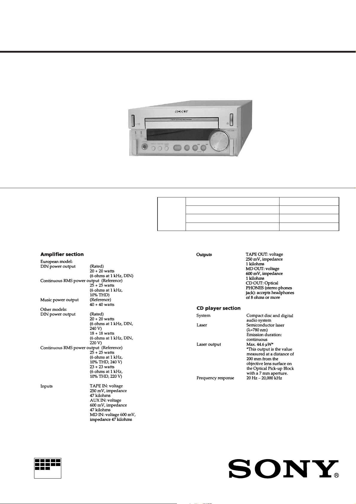
HCD-SD1
SERVICE MANUAL
HCD-SD1 is the amplifier, CD and
tuner section in CMT-SD1.
Model Name Using Similar Mechanism HCD-MD313
CD
SECTION
SPECIFICATIONS
Mechanism T ype CDM13B-5BD19
Base Unit Type BU-5BD19
Optical Pick-up Type KSS-213B/K-N
AEP Model
UK Model
E Model
MICROFILM
— Continued on next page —
COMPACT DISC RECEIVER
– 1 –
Page 2
Laser component in this product is capable of emitting radiation
exceeding the limit for Class 1.
This appliance is classified as
a CLASS 1 LASER product.
The CLASS 1 LASER PRODUCT MARKING is located on
the rear exterior.
This caution
label is located
inside the unit.
CAUTION
Use of controls or adjustments or performance of procedures
other than those specified herein may result in hazardous radiation exposure.
Notes on chip component replacement
• Never reuse a disconnected chip component.
• Notice that the minus side of a tantalum capacitor may be
damaged by heat.
Flexible Circuit Board Repairing
• Keep the temperature of soldering iron around 270˚C
during repairing.
• Do not touch the soldering iron on the same conductor of the
circuit board (within 3 times).
• Be careful not to apply force on the conductor when soldering
or unsoldering.
MODEL IDENTIFICATION
– Specification Label –
MODEL NO. HCD-SD1
SAFETY-RELATED COMPONENT WARNING !!
COMPONENTS IDENTIFIED BY MARK ! OR DO TTED LINE
WITH MARK ! ON THE SCHEMATIC DIAGRAMS AND IN
THE PARTS LIST ARE CRITICAL TO SAFE OPERATION.
REPLACE THESE COMPONENTS WITH SONY PARTS
WHOSE PART NUMBERS APPEAR AS SHOWN IN THIS
MANUAL OR IN SUPPLEMENTS PUBLISHED BY SONY.
– 2 –
MODEL
AEP, UK model
SP, HK model
• Abbreviation
HK : Hong Kong model
SP : Singapore model
Parts No.
PARTS No.
4-212-711-0π
4-212-712-0π
Page 3

TABLE OF CONTENTS
1. SERVICING NOTE .......................................................... 4
2. GENERAL ..........................................................................7
3. DISASSEMBLY
3-1. Loading Panel ....................................................................... 8
3-2. Glass ASSY...........................................................................8
3-3. Front Panel ........................................................................... 9
3-4. Main Board and Tuner Unit .................................................. 9
3-5. CD Mechanism Deck .......................................................... 10
3-6. Back Panel ......................................................................... 10
3-7. Disc Table .......................................................................... 11
3-8. Optical Pick-up ................................................................... 11
4. SERVICE MODE .............................................................12
5. TEST MODE ..................................................................... 13
6. ELECTRICAL ADJUSTMENTS ............................... 14
7. DIAGRAMS
7-1. Circuit Boards Location ...................................................... 16
7-2. Block Diagrams
• BD Section .......................................................................17
• Main Section .................................................................... 19
7-3. Schematic Diagram – BD Section – ................................... 23
7-4. Printed Wiring Board – BD Section –................................. 25
7-5. Schematic Diagram – Main (1/2) Section –........................ 27
7-6. Schematic Diagram – Main (2/2) Section – ........................ 29
7-7. Printed Wiring Board – Main Section – .............................. 31
7-8. Schematic Diagram – Sub Trans Section –.........................33
7-9. Printed Wiring Board – Sub Trans Section – ...................... 34
7-10. Schematic Diagram – Panel Section – ............................. 35
7-11. Printed Wiring Board – Panel Section –...........................37
7-12. Schematic Diagram – AMP Section –.............................. 39
7-13. Printed Wiring Board – AMP Section – ........................... 41
7-14. Schematic Diagram – Connector Section –...................... 43
7-15. Printed Wiring Board – Connector Section – ................... 45
7-16. Schematic Diagram – REG Section – .............................. 47
7-17. Printed Wiring Board – REG Section –............................ 49
7-18. IC Block Diagrams ........................................................... 51
7-19. IC Pin Functions ............................................................... 54
NOTES ON HANDLING THE OPTICAL PICK-UP BLOCK
OR BASE UNIT
The laser diode in the optical pick-up block may suffer electrostatic
break-down because of the potential difference generated by the
charged electrostatic load, etc. on clothing and the human body.
During repair, pay attention to electrostatic break-down and also
use the procedure in the printed matter which is included in the
repair parts.
The flexible board is easily damaged and should be handled with
care.
NOTES ON LASER DIODE EMISSION CHECK
The laser beam on this model is concentrated so as to be focused on
the disc reflective surface by the objective lens in the optical pickup block. Therefore, when checking the laser diode emission, observe from more than 30 cm away from the objective lens.
LASER DIODE AND FOCUS SEARCH OPERATION
CHECK
Carry out the “S curve check” in “CD section adjustment” and check
that the S curve waveform is output two times.
8. EXPLODED VIEWS
8-1. Front Panel Section ............................................................. 56
8-2. Chassis Section ................................................................... 57
8-3. Mechanism Deck Section (CDM13B-5BD19) ................... 58
8-4. Base Unit Section (BU-5BD19).......................................... 59
9. ELECTRICAL PARTS LIST ........................................ 60
– 3 –
Page 4
SECTION 1
SERVICING NOTE
OPENING THE DISC TRAY WHEN POWER IS OFF
1
Using a thin screwdriver, rotate the internal cam
in the arrow direction completely.
2
Open the glass door, and pull out the loading panel.
ATTACHING THE GLASS ASSEMBLY
• Attach according to steps 1 to 4.
2
Pull up the glass door,
in the arrow direction.
1
1
3
Bracket (shaft)
4
Screw (PTP 2.6x6)
(Bottom side)
– 4 –
When securing this part, position at the
center to allow some play. Open and close
the glass window sever al times, and check
that the parts do not touch each other.
Page 5
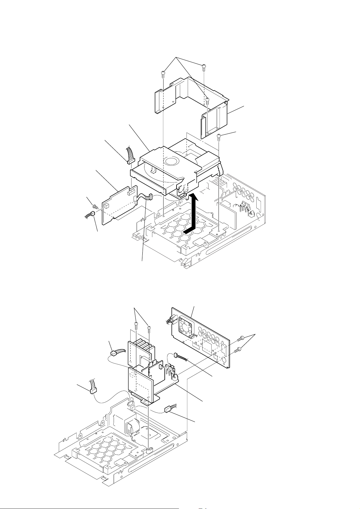
POSITIONS FOR SERVICING THE CONNECTOR
d
BOARD , SUB-TRANS BO ARD, CHEMI-CON BO ARD,
AND AMP BOARD
1 Remove the four screws securing the upper cover, and remove
the upper cover.
2 Remove the loading panel. (Refer to SECTION 3 DISASSEM-
BLY.)
3 Remove the four screws A securing the MAIN board, five screws
B securing the rear panel, two flat cables (CN701, CN702),
and open the MAIN board as shown in the figure.
4 Remove the two screws C securing the heat sink, and remove
the AMP board and CHEMI-CON board.
5 Remove the two screws D securing the SUB-TRANS board
and four screws E securing the CONNECTOR board, and remove the SUB-TRANS board and CONNECTOR board.
6 Return the MAIN board to its original position.
7 Insulate these boards and the MAIN board with paper, etc., and
assemble the CONNECTOR board, SUB-TRANS board,
CHEMI-CON board, and AMP board on these boards.
SUB-TRANS board
Heat sink
D
C
AMP board
CHEMI-CON board
CONNECTOR board
B
B
Flat type wire (CN701)
E
MAIN boar
A
A
Flat type wire (CN702)
– 5 –
Should be insulatable
with paper, etc.
Page 6
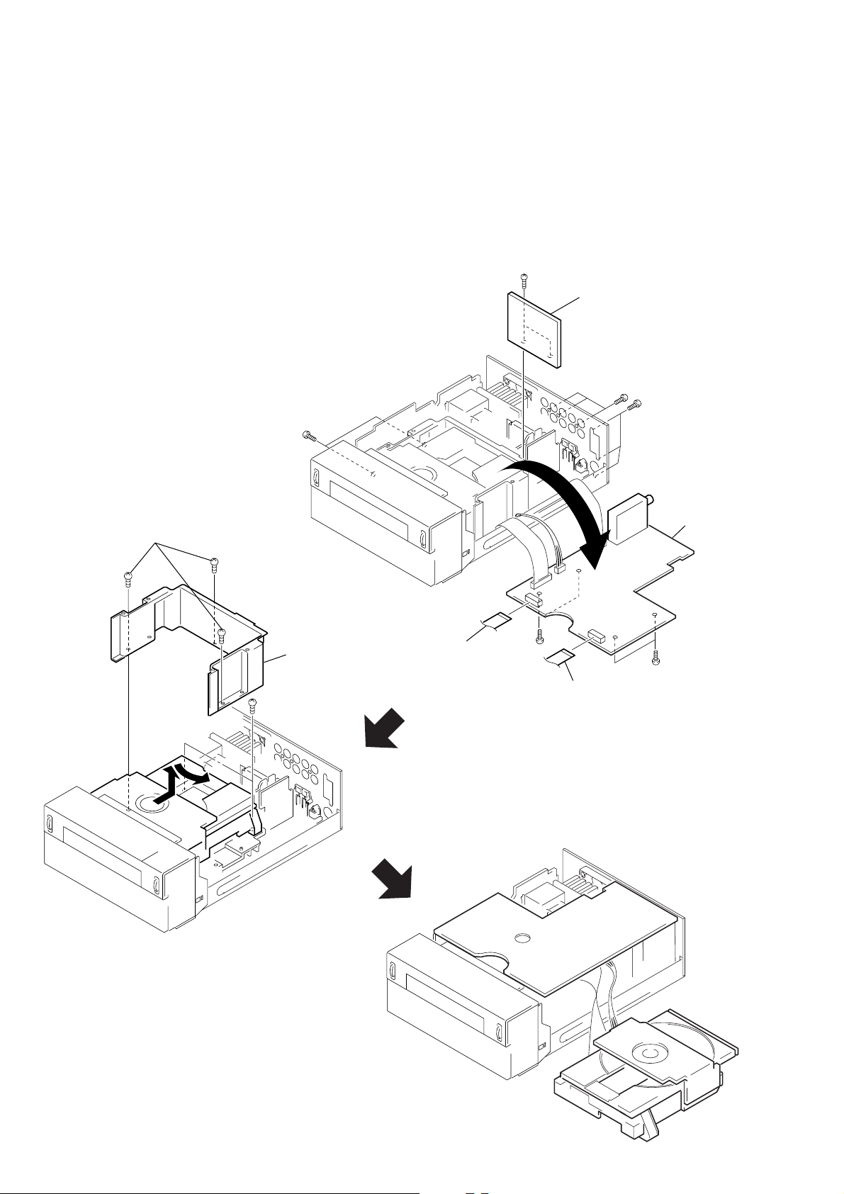
POSITION FOR SERVICING THE CD MECHANISM
r
DECK
1 Remove the four screws securing the upper cover, and remove
the upper cover.
2 Remove the loading panel. (Refer to SECTION 3 DISASSEM-
BLY.)
3 Remove the four screws A securing the MAIN board, five screws
B of the rear panel, and flat cables (CN701, CN702), and re-
move the MAIN board.
4 Remove the two screws D securing the SUB-TRANS board,
and remove the SUB-TRANS board.
5 Remove the two screws F securing the REG board.
6 Remove the three screws G securing the CDM cover, and re-
move the CDM cover.
7 Remove the two screws H securing the CDM, move the CDM
backwards by about 5 mm horizontally, and then lift upwards.
8 Rotate the CDM in the counterclockwise direction by about 30˚
to remove.
9 Return the MAIN and SUB-TRANS boards to their original
positions.
F
G
D
SUB-TRANS board
B
B
MAIN board
H
CDM cove
Flat type wire (CN701)
A
A
Flat type wire (CN702)
– 6 –
Page 7
Front Panel
15
14
13
SECTION 2
GENERAL
1
2
3
4
12
Location of Parts and Controls
1 1/u (Power) button
2 CD disc tray
3 § button
4 VOLUME dial
5 ±/)/TUNING + button
11
6 ≠/0/TUNING – button
7 π button
8 fl button
9 TUNER/BAND button
10 FUNCTION button
78910
6
5
11 DISPLAY button
12 PHONES jack
13 t indicator
14 u indicator
15 Display window
This section is extracted from
instruction manual.
– 7 –
Page 8
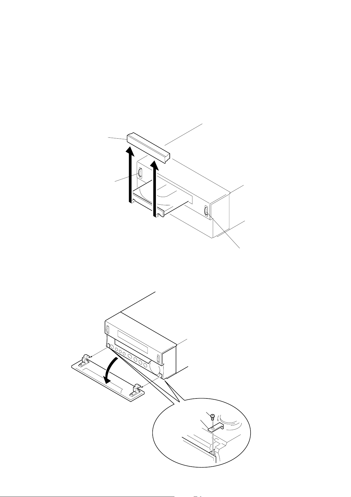
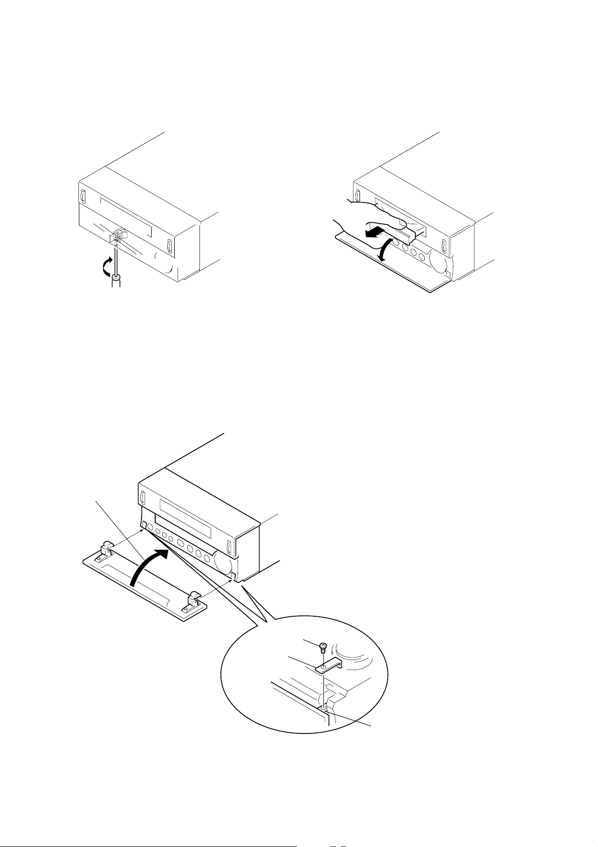
SECTION 3
n
DISASSEMBLY
Note: Follow the disassembly procedure in the numerical order given.
3-1. LOADING PANEL
1 Turn ON the power, and press the EJECT button to open the
tray.
2 Remove the loading panel in the arrow direction.
3 Press the EJECT button to close the tray.
• If the power cannot be turned ON, refer to “Opening the Disc
Tray When the Power is OFF” of “Service Note”, and open the
tray.
Loading panel
Power button
3-2. GLASS ASSY
4
3
4
1
Screw (PTP2.6x6)
2
Bracket (shaft)
Eject butto
– 8 –
(Bottom side)
Page 9
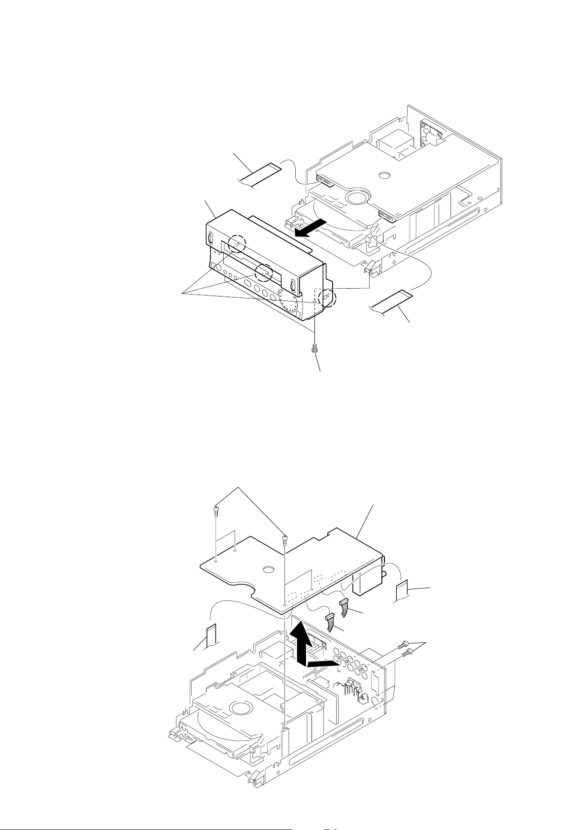
3-3. FRONT PANEL
2
Three claws
6
Front panel
4
Flat type wire (11core)
(CN702)
3
5
Flat type wire (13core)
(CN701)
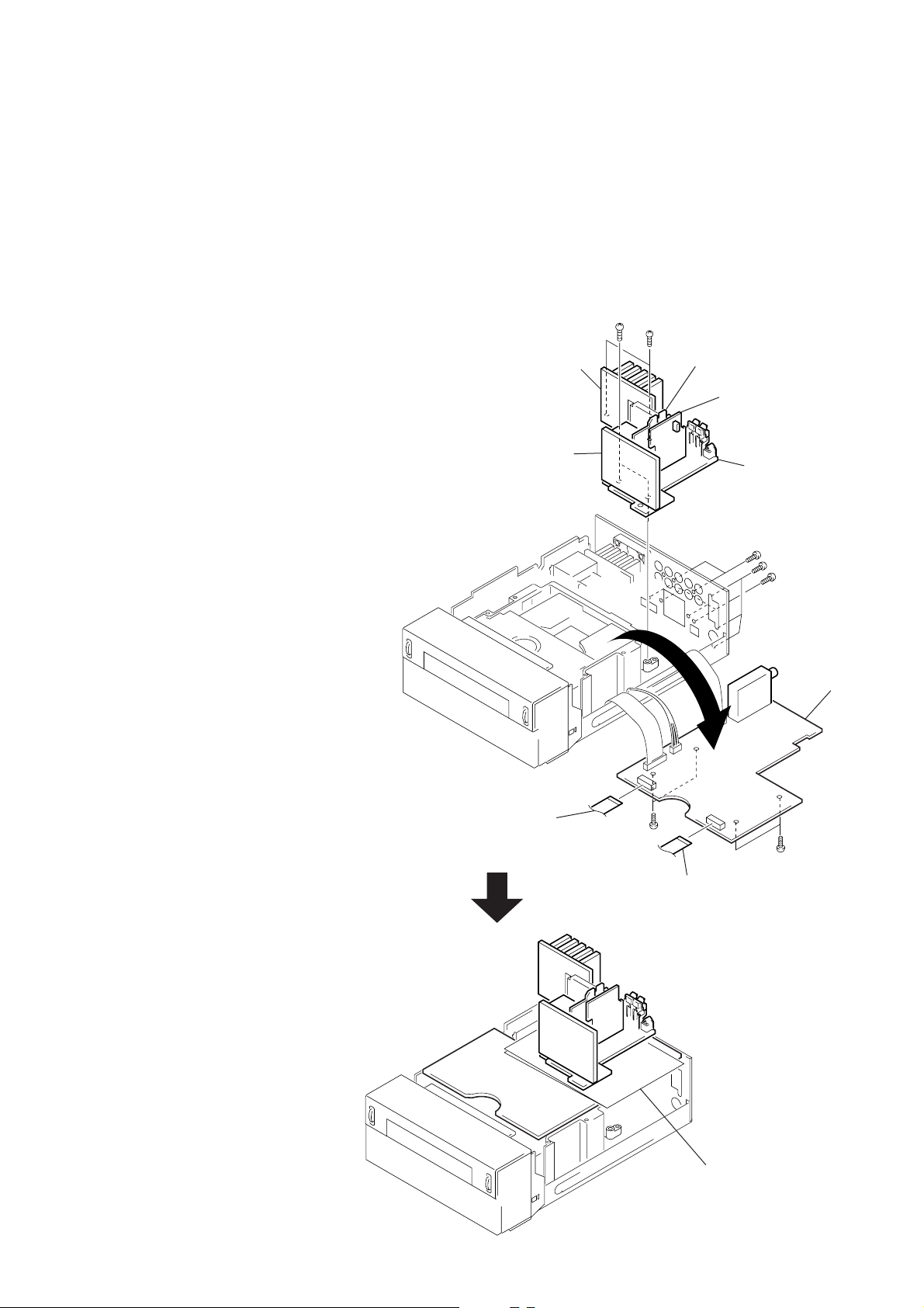
3-4. MAIN BOARD AND TUNER UNIT
1
Four screws
(BVTP3x8)
4
Flat type wire (19core)
(CN301)
1
Three screws
(BVTP3x8)
3
7
MAIN board and Tuner unit
8
Connector (CN706)
5
Connector (CN351)
6
Flat type wire
(19core) (CN705)
2
Six screws
(BVTP3x8)
– 9 –
Page 10
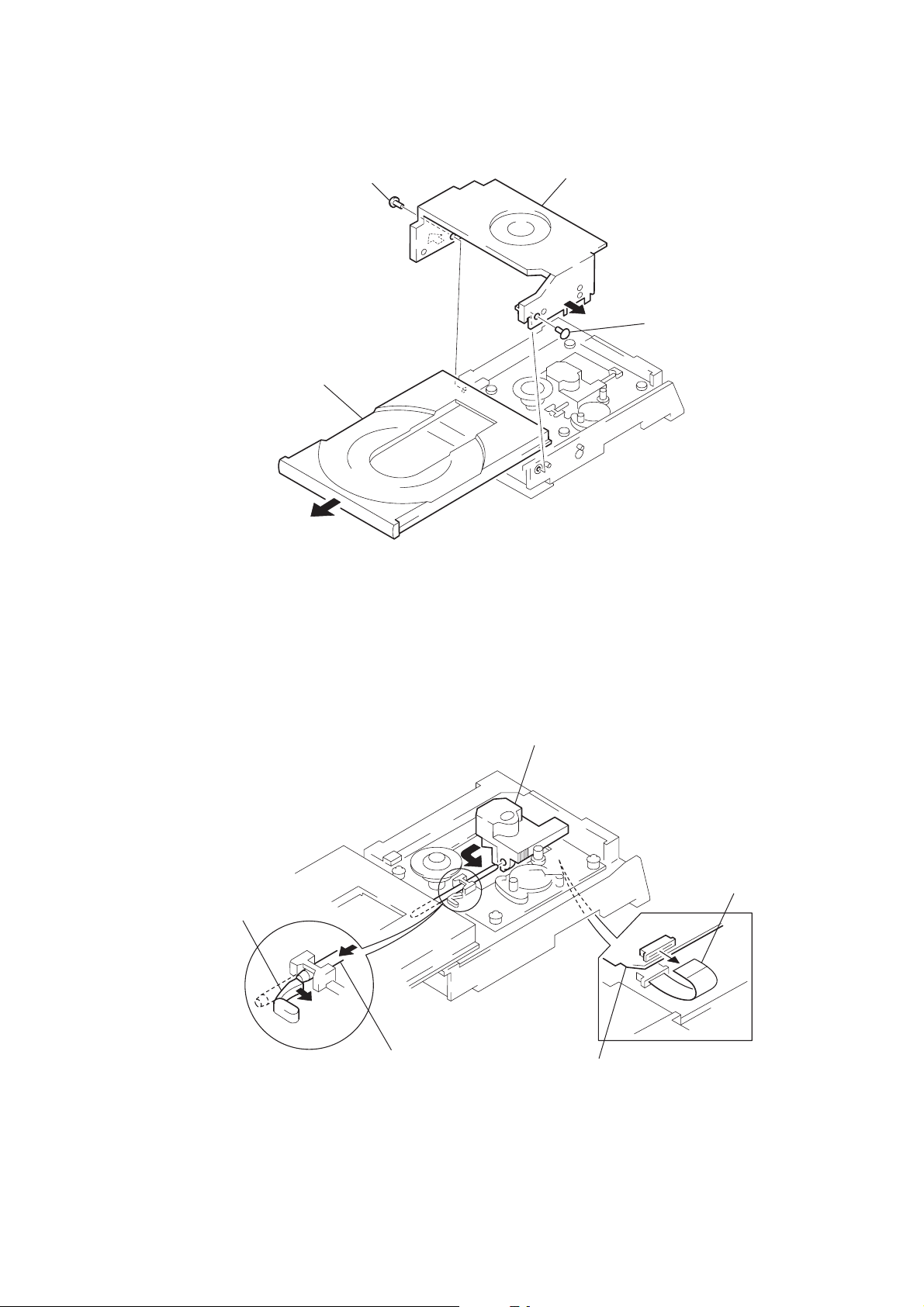
3-5. CD MECHANISM DECK
r
3
Connector
(CN942)
5
REG board
1
T wo screws
(BVTP3x8)
9
CD mechanism deck
6
Three screws
(BVTP3x8)
7
Dust cove
8
T wo screws
(BVTP3x8)
3-6. BACK PANEL
3
Connector
(CN992)
2
Connector
(CN945)
5
Connector
(CN901)
4
Connector
(CN994)
2
Four screws
(BVTT3X8)
7
Back panel
6
Connector
(CN551)
8
PC board block
1
Six screws
(BVTP3X8)
– 10 –
4
Connector
(CN991)
Page 11
3-7. DISC TABLE
)
1
Screw (BV3x8)
4
Pull out the disc table.
3
Holder (MG) assembly
2
Screw (BV3x8
3-8. OPTICAL PICK-UP
1
Move the claw
in the arrow
A
direction.
4
Remove the optical pickup in the arrow direction C.
B
A
2
Remove the sled shaft in the
arrow direction
B
.
C
Flat type wire (16 core)
3
(CNU101)
BD board
– 11 –
Page 12
SECTION 4
SERVICE MODE
Key Check Mode for Complete Lighting of LED/Fluorescent Display Tube
• Perform this mode to analyze and check malfunctions such as display defects and when buttons do not work.
Procedure:
1. Press the 1/u button to turn on the power.
2. Press the DISPLAY button and ^ button together.
3. All LEDs and the fluorescent display tube will light up completely.
4. Pressing the FUNCTION button here will light the fluorescent display tube in the following order; Partial lighting 1 n Partial lighting
2 n Complete lighting n Partial lighting 1······
Turning the VOLUME dial will switch the lighting order of the LED.
To end without shifting to the key check mode, press the 1/u button to end.
5. Pressing the p button sets the key check mode.
6. During the key check mode, “KEY=0 JOG=0” will be displayed on the fluorescent display tube.
Pressing a button will increase the value of “KEY=”. However the value will not increase for buttons which have already been pressed
once.
Rotating the VOLUME knob in the clockwise direction increases the value of “JOG=” in the order of 1, 2, 3.... and rotating in the
counterclockwise direction decreases in order of 10, 9, and 8.
7. To end the check mode, press all buttons (8 buttons). “KEY-OK” will be displayed.
Then press any button, and disconnect the power cord from the outlet.
Checking the Sub-Clock
• Perform this mode to check clock operations.
Procedure:
1. Connect an oscilloscope and frequency counter between the pin (TP791) and ground of IC701 of the MAIN board.
2. Press the § and 1/u buttons together to display “91P = 32.768k” on the fluorescent display tube.
3. Check that the signal on the oscilloscope becomes a 32 kHz rectangular waveform and the reading of the frequency counter becomes
32.768 kHz.
4. Press the 1/u button to end.
Sled Servo Mode
• In this mode, the CD sled motor can be operated freely.
Execute it when cleaning the pick-up.
Round holes can be seen on the topmost board when the case is opened. Move the pick-up and clean off the dirt in these round holes using
a cotton swab.
Procedure:
1. Press the DISPLAY and § buttons with the power of the unit OFF.
2. When the sled servo is set, “MANUAL” is displayed on the fluorescent display tube.
3. Pressing the +/TUNING/) button when the CD is in the stop state moves the pick-up to the outer track. Pressing the =/
TUNING/0 button moves it to the inner track.
4. To end this mode, perform the following steps.
1) Move the If not, the disc cannot be removed.
2) Press the DISPLAY and § buttons together.
Note:
• When ending this mode, be sure to move the pick-up to the innermost circumference. If not, the disc cannot be removed.
• Do not move the sled motor more than required as this will damage the gears.
Round holes for cleaning
Initializing (Forced Reset)
• Perform this mode when resetting the unit or when returning the unit to the customer.
• The preset frequency of the tuner, etc. will be the settings at shipment.
Procedure:
While pressing the 1/u button, insert the power cord into the outlet.
– 12 –
Page 13
SECTION 5
TEST MODE
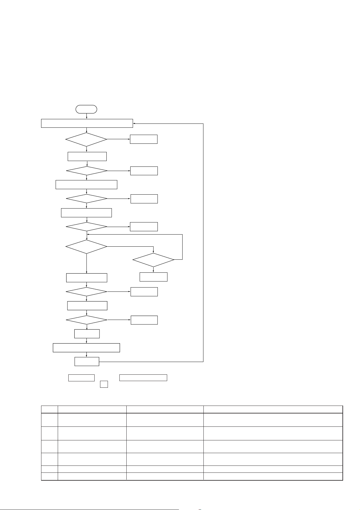
AGING MODE
This unit is equipped with an aging mode.
Use this mode for analyzing defects and for checks after completing repairs.
After repairs, perform aging 100 times and check that the unit is normal.
The aging mode is executed in the following sequence.
The aging mode will continue as long as the unit is normal.
If the unit becomes abnormal, it will display the state and number of cycles, and operations will stop. (Refer to Table 1.)
Sequence of Aging Mode:
Start
Sets the CD function and reads the CD TOC.
CD TOC OK?
YES
Pauses first song.
OK?
YES
Last song search paused state
OK?
YES
Starts last song playback
OK?
YES
End playback?
YES
Opens the CD tray
OK?
YES
Closes the CD tray
NO
NO
NO
NO
NO
NO
Message 1
Message 2
Message 3
Message 4
Is CD playing?
Message 4
Message 5
OK
NG
OK?
YES
Power OFF
Display of number of aging cycles
Power ON
NO
Message 6
Procedure:
1. Press the DISPLAY button and =/TUNING/0 button together.
2. To end aging, press the u button and end.
Table-1 Messages and Main Reasons for Stop of Aging
No
1
2
Error Messages
CD No Disc NG
CD Pause NG
Details of Error
Cannot read CD TOC.
Cannot set CD pause in
CD synchro mode.
3
4
5
6
CD Search NG
CD Play NG
CD Open NG
CD Close NG
Cannot search last track on CD.
Cannot play last track on CD.
Cannot open CD tray.
Cannot close CD tray.
Main Causes
Optical defect, spindle defect (including motor), cannot read
Q data, disc defect (scratches, etc.), bad focus, bad GFS, etc.
Disc defect (scratches, etc.), cannot read Q data, etc.
Optical defect, sled, tracking defect (including motor), cannot
read Q data, disc defect (scratches, etc.).
Optical defect, cannot read Q data, disc defect (scratches, etc.),
etc.
LOAD OUT SW defect
LOAD IN SW defect
– 13 –
Page 14
–
+
oscilloscope
BD (CD) board
TP (RF)
TP (VC)
SECTION 6
ELECTRICAL ADJUSTMENTS
CD SECTION
Note:
1. CD Block is basically designed to operate without adjustment.
Therefore, check each item in order given.
2. Use YEDS-18 disc (3-702-101-01) unless otherwise indicated.
3. Use an oscilloscope with more than 10MΩ impedance.
4. Clean the object lens by an applicator with lens cleaning liquid
when the signal level is low than specified value with the following checks.
5. Adjust the focus bias adjustment when optical block is replaced.
Focus Bias Adjustment
Perform this adjustment when the optical pick-up has been replaced
or repaired.
oscilloscope
BD (CD) board
TP (RF)
TP (VC)
Procedure:
1. Connect oscilloscope to test point TP (RF).
2. Turned Power switch on.
3. Put disc (YEDS-18) in and playback.
4. Adjust RV101 so that the waveform is clear.
(Clear RF signal waveform means that the shape “◊” can be
clearly distinguished at the center of the waveform.)
5. After adjustment, check the RF signal level.
• RF signal
VOLT/DIV: 200 mV
TIME/DIV: 500 nS
+
–
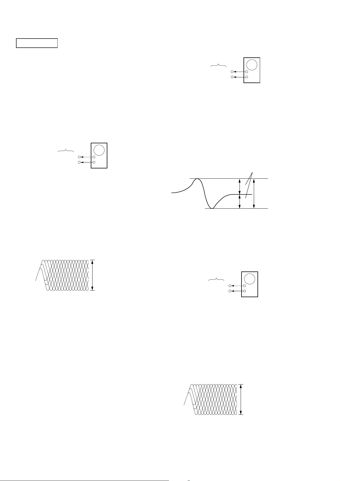
S Curve Check
oscilloscope
BD (CD) board
TP (FEO)
TP (VC)
+
–
Procedure :
1. Connect oscilloscope to test point TP (FEO).
2. Connect between test point TP (FOK) and Ground by lead wire.
3. Turn Power switch on.
4. Put disc (YEDS-18) in and turned Power switch on again and
actuate the focus search. (actuate the focus search when disc
table is moving in and out.)
5. Chec k the oscilloscope waveform (S-curve) is symmetrical between A and B. And confirm peak to peak level within 2.4 ± 0.7
Vp-p.
S-curve waveform
symmetry
A
±
within 2.4
B
0.7 Vp-p
6. After check, remove the lead wire connected in step 2.
Note: • Try to measure several times to make sure than the ratio of
A : B or B : A is more than 10 : 7.
• Tak e sweep time as long as possible and light up the brightness to obtain best waveform.
RF Level Check
level : 1.3 ± 0.3 Vp-p
Procedure :
1. Connect oscilloscope to test point TP (RF) on BD board.
2. Turned Power switch on.
3. Put disc (YEDS-18) in and playback.
4. Confirm that oscilloscope waveform is clear and check RF signal level is correct or not.
Note: Clear RF signal waveform means that the shape “◊” can be
clearly distinguished at the center of the waveform.
• RF signal
VOLT/DIV: 200 mV
TIME/DIV: 500 nS
level : 1.3 ± 0.3 Vp-p
– 14 –
Page 15
E-F Balance (1 Track Jump) Check
V
RF
RV101
(Focus Bias Adjust)
RV103
TEO
VC
FEO
RV102
TEI
FEI
FOK
IC101
IC104
GND
PCK
IC102
(Without remote commander)
oscilloscope
BD (CD) board
Adjustment Location:
[BD (CD) BOARD] — Component Side —
TP (TEO)
TP (VC)
+
–
Procedure :
1. Connect oscilloscpe to test point TP (TEO) on BD board.
2. Turn Power switch on.
3. Put disc (YEDS-18) in to play the number five track.
4. Press the “P (P ause)” button. (Becomes the 1 track jump mode)
5. Confirm that the oscilloscope waveform is symmetrical on the
top and bottom in relation to 0Vdc, and check this level.
1 track jump waveform
A
0
B
LEVEL : 300 ± 100 mVp-p
Specified level: • x 100 = less than ± 7%
A – B
2 (A + B)
• A + B = 300 ± 100 mVp-p
Focus/Tracking Gain Adjustment (RV102, RV103)
This gain has a margin, so even if it is slightly off.
There is no problem.
Therfore, do not perform this adjustment.
Please note that it should be fixed to mechanical center position
when you moved and do not know original position.
– 15 –
Page 16

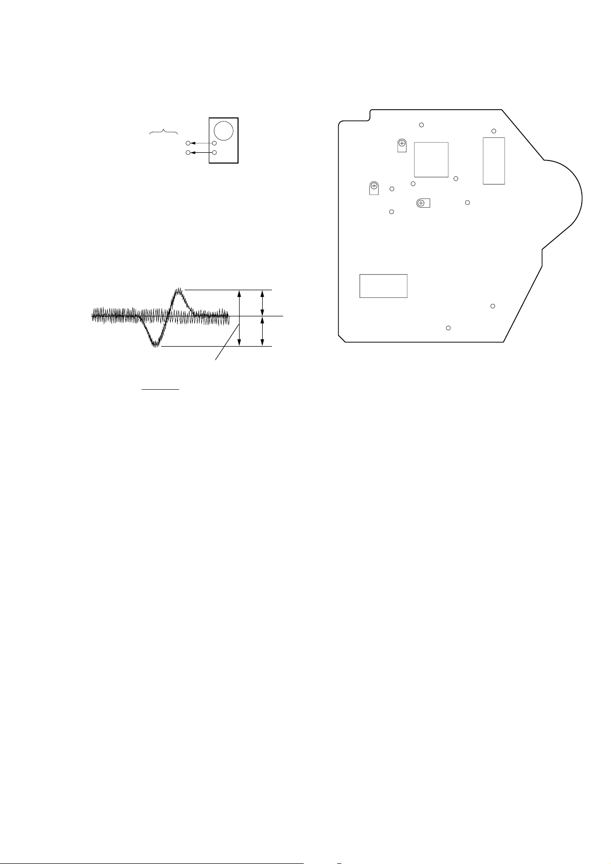
7-1. CIRCUIT BOARDS LOCATION
d
PANEL-SW board
SECTION 7
DIAGRAMS
TRANS board
MAIN board
PANEL board
SUB-TRANS board
BD board
LOADING board
AMP board
REG board
CHEMI-CON boar
HP board
CONNECTOR board
VOLUME board
– 16 –
Page 17

7-2. BLOCK DIAGRAMS
– BD SECTION –
OPTICAL PICK-UP
DETECTOR
E
A
B C
(KSS-213B)
B+
K
A
D
D
C
B
F
HCD-SD1
X101
22.5792 MHz
TRACKING/FOCUS SERVO,
RF AMP
IC101 (1/2)
1
4
2
5
10
6
RV102
FOCUS
GAIN
PD1
35
36
PD2
F
38
39
E
2
FEI
RFO
C.OUT
SENS
FE BIAS
31
30
RFI
23
24
RV101
FOCUS
BIAS
37
+5V
RF
14
DIGITAL SIGNAL PROCESSOR
CNIN
55
SEIN
54
DATAO56XLTO57CLKO59MDP3FOK1XLON
64
IC103
DATA51XLAT52CLOK53SCOR43SQSO46SQCK47SENS49XRST50D OUT
SPOD
63
34
39
XTAI
PCMD
LRCK
BCLK
4
5 • 6
•
XTI
XTO
CKO
DATA
21
20
2
LRCK
1
BCLK
322
LOUT
ROUT
DATA26MLAT28CLOK
27
16
13
DIGITAL FILTER
D/A CONVERTER
IC104
CD LOUT
MAIN
A
SECTION
(Page 19)
LASER
DIODE
PD LD
FOCUS
COIL
SLED/SPINDLE
MOTOR DRIVE
IC102 (2/2)
TRACKING
COIL
2-AXIS
DEVICE
RV103
TRACKING
GAIN
LD DRIVE
Q101, 102
T+
T–
F–
F+
1
FEO
42
TEO
44
TEI
33
LD
34
PHD
XRST
22
7
XRST
18
17
12
11
TRACKING
COIL DRIVE
TRACKING/FOCUS
COIL DRIVE
IC102 (1/2)
FOCUS
COIL DRIVE
SLED
SERVO
IC101 (2/2)
FE-O
FE-M
TA-M
TAO
DATA
XLT
CLK
FOK
FGD
6
7
12
13
21
20
19
25
4
19
9
FOCUS SW
Q103
S101
(LIMIT)
M904 (CD)
LOADING
MOTOR
D OUT
CLK
DATA
XRST
SCOR
SENS
SQCK
SQSO
DF LAT
XLAT
FOCUS SW
MOTOR
DRIVER
IC351
2
DRIVE
5
LOAD-OUT
M
10
DRIVE
6
LOAD-IN
MAIN
A
SECTION
(Page 19)
MAIN
A
SECTION
(Page 19)
M102
SLED MOTOR
M101
SPINDLE
MOTOR
09
• SIGNAL PATH
: CD
: Digital out
26
•
M
27
1
•
M
2
SLED MOTOR
DRIVE
SPINDLE MOTOR
DRIVE
25
4
– 17 –
16
SLO
SL+
14
S291
(LOAD OUT)
S292
(LOAD IN)
OUT-SW
IN-SW
– 18 –
Page 18

HCD-SD1
– MAIN SECTION –
ANTENNA
AM
FM
75Ω
J101
(1/2)
L
IN
MD
R
J102
(1/2)
L
IN
CS/BS
R
L
IN
TAPE
R
FLUORESCENT INDICATOR TUBE
VF1
VF0
–VG
BUFFER
Q601
TUNER
UNIT
L-OUT
R-OUT R-CH
STEREO
TUNED
MUTING
FM-DET-OUT
R-CH
BS
R-CH
R-CH
R-CH
IN
4
FL601
56
51
ST
TUN
MUT
DO
DO
CL
CL
DI
DI
CE
CE
12
13
2
1
RDS DECODER
IC451
DATA
14
13
X601
4.3 MHz
5 – 50
VFL
DAT
G12
63 62 61 60
DISPLAY DRIVER
IC601
BUFFER
Q450
SWITCH
IC102
9 10 11
SWITCH
Q103
INT
16
2
CLKCSRST
14
15
R-CH
CD SECTION
(Page 18)
A
SIRCS
IC602
LOUT
R-CH
CD
TUNER
BS/CS
MD
CD
LAT
DAT
CLK
FOCUS SW
DF-LAT
IN SW
OUT SW
LOAD IN
LOAD OUT
D OUT
SOUND PROCESSOR
4
5
6
7
39
38
37
36
20
LATCH
DATA
21
CLOCK
22
90
DAT
65
CLK
66
LAT
67
ST
82
TUN
83
DO
84
DI
85
CL
86
CE
87
MUT
88
100
38
37
36
35
20
21
SCOR
22
SQSO
43
SQCK
45
52
SENS
53
CLK
57
DAT
58
59
XLAT
60
XRST
63
49
50
61
62
IC101(1/2)
• VOLUME
SIRCS
SDATA
SCLOCK
SLAT1
STEREO
TUNED
ST.IDATA
ST.ODATA
ST.CLOCK
ST.LATCH
ST.MUTE
V/T
FL.RST
FL.LAT
FL.SLK
FL.DAT
RDS.CLK
RDS.DAT
SCOR
SQSI
SQCK
FSW
SENS
CD-CLK
CD-DATA
DF-LAT
DSP-LAT
BD.RESET
IN SW
OUT SW
LOAD IN
LOAD OUT
TREBLE
IC701
SP RELAY SW
15
8
28
35
ON/XSRBY
FLDISP SW
2
I C.CLOCK
ENCODERB
ENCODERA
TIMER LED
STBY LED
PANEL SW
BD POWER
BASS/
AMP
MASTER CONTROL
DEFB SW
Q121
R-CH
R-CH R-CH
TC-MUT
99
MD-MUT
98
MUTE2
69
76
MUTE1
68
31
HPSW
81
75
HELP
51
2
55
I C.DAT
56
26
KEY2
25
KEY1
19
18
XT1
14
XT2
13
11
X2
X1
10
73
72
ON LED
70
64
LIGHT
8
AC CUT
15
RESET
2
1
+8dB AMP
IC103
3
5 7
MUTE SW
Q183
MUTE SW
Q182
MUTE SW
Q181
SWITCH
Q753
X702
32KHz
X701
5MHz
SWITCH
Q752
RESET
Q751
PANEL SW
S699
S621-625,631-634
R-CH
R-CH
1
KEY BOARD
SWITCH
2
1
3 1
SOUND PROCESSOR
IC101(2/2)
16
DBFB
27
MUTE
Q111
MUTE
Q112
SWITCH
Q793
SWITCH
Q791
VOLUME
S691
t
TIMER:RED
D605
D601-604
RESET
IC951
TO IC701 VDD
SWITCH
Q943
18
25
AMP
R-CH
R-CH
u
ON:GREEN
STANDBY:RED
D606
D601
)/±
D752
SWITCH
Q792
R-CH
J101(2/2)
J102(2/2)
D602
0/≠
STBY+5.6V
D751
+
C759 BACK UP
L
MD
OUT
R
L
TAPE
OUT
R
D603
MUTE
Q141
LY
LXSYSX
2
I C BUS
EXTENDER
IC791
D604
π
fl
POWER AMP
IC801
10
+
3
–
9
8
MUTE
Q505
HLP
DAT
76
CLK
23
R-CH
D881
RELAY SW
Q502,503
RELAY SW
Q501
A±7.5VREG
D±5V
M+7V
CDD+5V
ST12V
STBY+5.6V
VG SWITCH
VF SWITCH
Q965
Q966
R-CH
A±7.5VREG
Q941, 946
3
D+5VREG
M+7VREG
3
CDD+5V SW
ST 12V OUT
Q951,952
SPEAKER RELAY
RY501
RELAY DRIVE
Q504
±B
1
IC921
1
IC922
Q942
3 1
VG
VF1
VF0
RECT
D971
RECT
D941-944
RECTIFIER
D921,922
RECTIFIER
Q951,953
STBY+5.6V REG
IC901
VG SW
Q964
VF SW
Q962,963
R-CH
UG REG
Q961
T991
MAIN
TRANSFORMAER
RECT
D901-904
RECT
D961-964
R-CH
FAN-DRIVE
Q551–553
R-CH
DAT
HLP
CLK
RY901
STANDBY RELAY
T991
SUB
TRANSFORMER
• R ch is same as L ch
• SIGNAL PATH
: FM
BS
:BS/CS
TMB11
+
–
–
+
FAN
CN781
1
2
5
IC311
DOUT
AC IN
AC OUTLET
CN904
L
R
J667
PHONES
SYSTEM
CONTROL
DIGITAL
OPTICAL
SPEAKER
INPEDANCE
6-16Ω
: PB
: REC
: CD
: Digital out
: TAPE
– 19 –
– 20 –
Page 19

HCD-SD1
2.6 Vp-p
7.6 µs
5.1 Vp-p
136 µs
4.6 Vp-p
16.9344 MHz
Approx.
150 mVp-p
THIS NOTE IS COMMON FOR PRINTED WIRING
BOARDS AND SCHEMATIC DIAGRAMS.
(In addition to this, the necessary note is printed
in each block.)
For schematic diagrams.
Note:
• All capacitors are in µF unless otherwise noted. pF: µµF
50 WV or less are not indicated except for electrolytics
and tantalums.
• All resistors are in Ω and 1/
specified.
¢
•
• 2 : nonflammable resistor.
• 1 : fusible resistor.
• C : panel designation.
Note: The components identified by mark ! or dotted line
• S : B+ Line.
• T : B– Line.
• H : adjustment for repair.
• Voltages and wav ef orms are dc with respect to ground in
• Voltages are taken with a VOM (Input impedance 10 MΩ).
• Waveforms are taken with a oscilloscope.
• Circled numbers refer to waveforms.
Signal path.
• Abbreviation
: internal component.
with mark ! are critical for safety.
Replace only with part number specified.
service mode.
Voltage var iations may be noted due to normal produc-
tion tolerances.
Voltage var iations may be noted due to normal produc-
tion tolerances.
F : FM
E : PB (MD)
m : PB (TAPE)
n : REC
J : CD
c : digital out
SP : Singapore model.
HK : Hong Kong model.
4
W or less unless otherwise
WAVEFORMS
– BD SECTION –
1
IC101 #¡ (RFO) (PLAY Mode)
500 mV/DIV, 500 ns/DIV
2
IC101 $¢ (TEI) (PLAY Mode)
50 mV/DIV, 1 µs/DIV
3
IC101 2 (FEI) (PLAY Mode)
50 mV/DIV, 1 µs/DIV
4
IC103 3 (MDP) (PLAY Mode)
5
IC103 @• (RFCK)
6
14 ns
IC103 @∞ (XPCK)
1.3 ± 0.3 Vp-p
Approx.
100 mVp-p
5.3 Vp-p
– MAIN SECTION –
1
4.3 Vp-p
5 MHz
IC701 !¡ (XI)
2
2.6 Vp-p
32 kHz
IC701 !¢ (XI)
For printed wiring boards.
Note:
• X : parts extracted from the component side
• p : parts mounted on the conductor side.
®
•
•
• b : Pattern from the side which enables seeing.
(The other layers' patterns are not indicated.)
Caution:
Pattern face side: Parts on the pattern face side seen from the
(Side B) pattern face are indicated.
Parts face side: Parts on the parts face side seen from the
(Side A) parts face are indicated.
: Through hole.
¢
: internal component.
• Indication of transistor
C
Q
EB
These are omitted
C
EB
These are omitted
7
5 Vp-p
474 ns
IC103 @™ (BCLK)
8
5.1 Vp-p
22.8 µs
IC103 @º (LRCK)
9
IC104 6 (XTO)
– 21 – – 22 –
Page 20

HCD-SD1
7-3. SCHEMATIC DIAGRAM – BD SECTION –
• See page 22 for Waveforms.
• See page 51 for IC Block Diagrams.
Note on Schematic Diagram:
• Voltages and waveforms are dc with respect to ground
under no-signal (detuned) conditions.
no mark : Stop
( ) : CD (PLAY)
* : Can not be measured.
(Page 29)
– 23 –
– 24 –
Page 21

7-4. PRINTED WIRING BOARD – BD SECTION –
• See page 16 for Circuit Boards Location.
HCD-SD1
• Semiconductor
Location
Ref. No. Location
IC103 C-1
Q101 B-3
Q103 C-3
• Semiconductor
Location
Ref. No. Location
IC101 B-1
IC102 B-1
IC104 C-3
Q102 B-1
OPTICAL PICK-UP
BLOCK
KSS-213BA/S-N
(Page 32)
– 25 – – 26 –
Page 22

HCD-SD1
7-5. SCHEMATIC DIAGRAM – MAIN (1/2) SECTION –
• See page 22 for Waveforms.
• See page 31 for Printed Wiring Board.
(Page 39)
(Page
29)
– 27 –
(Page
29)
– 28 –
Page 23

7-6. SCHEMATIC DIAGRAM – MAIN (2/2) SECTION –
• See page 22 for Waveforms.
• See page 31 for Printed Wiring Board.
• See page 53 for IC Block Diagrams.
• See page 54 for IC Pin Functions.
HCD-SD1
(Page
28)
(Page 43)
(Page 24)
(Page 43)
(Page 36)
(Page
28)
(Page 48)
(Page 35)
(Page 48)
– 29 – – 30 –
Page 24

HCD-SD1
• Semiconductor
Location
Ref. No. Location
D351 A-6
D751 G-5
D752 G-5
D753 G-6
D755 G-6
D791 B-5
D792 B-5
D793 B-5
IC101 C-3
IC102 D-2
IC103 A-1
IC351 A-5
IC701 C-6
IC791 B-6
IC951 G-6
Q103 D-2
Q111 B-1
Q112 C-1
Q121 D-4
Q141 C-4
Q181 D-4
Q182 D-4
Q183 D-4
Q211 B-1
Q212 C-1
Q222 B-3
Q241 B-4
Q751 G-7
Q752 B-7
Q753 C-6
Q781 F-8
Q782 F-8
Q783 F-8
Q791 B-6
Q792 B-6
Q793 C-6
7-7. PRINTED WIRING BOARD – MAIN SECTION –
• See page 16 for Circuit Boards Location.
R
OUT
L
R
IN
L
R
OUT
L
R
IN
L
R
IN
L
AEP, UK
(Page 45)
*1
JW734
JW735
R735
: MOUNT
: NO MOUNT
AEP, UK SP, HK
(Page 41)
(Page 46)
(Page 26)
(Page 37)
*1
X601
AEP, UK
– 31 – – 32 –
(Page 38)
(Page 50)(Page 50)
Page 25

HCD-SD1
7-8. SCHEMATIC DIAGRAM – SUB SECTION –
(Page 47)
11EQS04
11EQS04
11EQS04
11EQS04
11ES2-NTA2B
11ES2NTA2B
11ES2NTA2B
11ES2-NTA2B
DTC114ESA
DTA114ESA-TP
7-9. PRINTED WIRING BOARD – SUB SECTION –
• See page 16 for Circuit Boards Location.
(Page 49)
(Page 43)
DTA114ESA-TP
(Page 45)
• Semiconductor Location
Ref. No. Location
D901 B-2
D902 B-1
D903 B-1
D904 B-1
D905 C-2
D906 B-3
D961 B-2
D962 B-2
D963 B-2
D964 B-2
D965 C-2
Ref. No. Location
D966 C-1
IC901 C-2
Q901 B-3
Q961 C-2
Q962 B-3
Q963 C-3
Q964 C-3
Q965 C-2
Q966 C-2
– 33 –
– 34 –
Page 26

HCD-SD1
7-10. SCHEMATIC DIAGRAM – PANEL SECTION –
(Page 30)
(Page 30)
– 35 – – 36 –
Page 27

7-11. PRINTED WIRING BOARD – PANEL SECTION –
• See page 16 for Circuit Boards Location.
HCD-SD1
(Page 32)
(Page 32)
E
• Semiconductor
Location
Ref. No. Location
D601 C-3
D602 C-3
D603 C-4
D604 C-5
D605 B-7
AEP, UK
D606 B-7
IC601 B-5
IC602 B-2
Q601 C-3
– 37 –
– 38 –
Page 28

HCD-SD1
7-12. SCHEMATIC DIAGRAM – AMP SECTION –
(Page 47, 48)
(Page 28)
– 39 – – 40 –
(Page 43)
Page 29

7-13. PRINTED WIRING BOARD – AMP SECTION –
• See page 16 for Circuit Boards Location.
HCD-SD1
• Semiconductor
Location
Ref. No. Location
D553 A-5
D554 A-5
D971 A-5
D972 A-5
Q505 B-4
Q551 A-5
Q552 A-5
Q553 A-4
(Page 50)
(Page 31)
(Page 45)
– 41 –
– 42 –
Page 30

HCD-SD1
7-14. SCHEMATIC DIAGRAM – CONNECTOR SECTION –
(Page 30)
(Page 29)
(Page 40)
(Page 33)
– 43 – – 44 –
Page 31

7-15. PRINTED WIRING BOARD – CONNECTOR SECTION –
11
(11)
CN291
S291
(LOAD OUT)
1
2
3
4
5
M904
(LOADING
MOTOR)
M
LOADING BOARD
S292
(LOAD IN)
1-634-461-
(Page 32)
• See page 16 for Circuit Boards Location.
(Page 31, 32)
(Page 34)
DIGITAL
OPTICAL
CD AUX
HCD-SD1
• Semiconductor
Location
Ref. No. Location
D501 B-3
D556 B-3
D557 C-3
D881 D-2
IC311 B-5
Q501 B-2
Q502 B-2
Q503 B-3
Q504 B-3
(Page 42)
AEP, UK
SPEAKER
INPEDANCE
SYSTEM
CONTROL
– 45 –
– 46 –
Page 32

HCD-SD1
7-16. SCHEMATIC DIAGRAM – REG SECTION –
(Page 40)
(Page 29)
(Page 29)
(Page 33)
– 47 – – 48 –
Page 33

7-17. PRINTED WIRING BOARD – REG SECTION –
• See page 16 for Circuit Boards Location.
AC
OUTLET
MDS-SD1
ONLY
UNSWITCHED
200W MAX
HCD-SD1
NOT REPLACEABLE:
BUILT IN TRANSFORMER
(Page 34)
(Page 32)
(Page 32)
(Page 42)
• Semiconductor
Location
Ref. No. Location
D921 A-4
D922 A-4
D941 A-4
D942 A-4
D943 A-4
D944 A-4
D945 B-2
D946 B-1
D952 B-1
– 49 –
IC921 B-3
IC922 B-3
Q941 B-2
Q942 C-2
Q943 C-2
Q951 A-1
Q952 B-1
– 50 –
Page 34

HCD-SD1
A
7-18. IC BLOCK DIAGRAMS
• BD section
IC101 CXA1782BQ
PHD2
37FE BIAS
38F
39E
40EI
41VEE
42TEO
43LPFI
44TEI
45ATSC
46TZC
47TDFCT
48VC
PHD1
36
35 34
BAL1
TOG1
• WINDOW COMP
PHD
–
RF IV AMP1
RF IV AMP2
F IV AMP
E IV AMP
BAL2
TOG2
ATSC
–
+
+
–
APC
–
+
–
+
BAL3
TOG3
+
–
+
–
+
TE AMP
+
FE AMP
1
FEO
IC102 BA6397FP
GND
OUT4
OUT4B
IN4A
28
27
26
LD
33
–
+
RF M
32
–
+
–
+
LEVELS
+
–
FOK
TTL
IIL
FZC COMP
–
DFCT
3
2
FEI
FDFCT
DFCT
FS4
31
–
–
+
–
+
–
+
+
–
TZC COMP
RF O
–
+
RF I
30
–
+
+
+
–
MIRR
• IIL DATA RESISTOR • INPUT SHIFT RESISTOR
TOG1-3 FS1-4 TG1-2 TM1-7 PS1-4
BAL1-3
–
+
HPF COMP LPF COMP
• FCS PHASE
COMPENSATION
TM1
5
4
FLB
FGD
–
+
FS2
+
–
6
FE O
+
–
• ADDRESS DECODER
• OUTPUT DECODER
TG1
FS1
7
FE M
CB
29CP28
DFCT
• TRACKING
• PHASE
COMPENSATION
9
8
SRCH
TGU
–
TM7
TG2
+
TM6
TM5
TM4
TM3
CC126CC225FOK
27
–
+
24 SENS
IIL
TTL
23 C. OUT
22 XRST
TTL
21 DATA
20 XLT
IIL
19 CLK
18 VCC
IC103 CXD2507AQ
FOK
MON
MDP
• ISET
17 ISET
MDS
LOCK
TEST
FILO
–
16 SL 0
+
FILI
PCO
VSS
15 SL M
AVSS
CLTV
AVDD
TM2
14 SL P
+
1312TA O
–
RF
BIAS
ASYI
ASYO
ASYE
WDCK
• F SET
11
10
TG2
FSET
TA M
DRIVE
BUFFER
1
2
3
4
5
6
7
8
9
10
11
12
13
14
15
16
17
18
19
DRIVE
BUFFER
1
OUT1A
2
OUT1B
SERVO AUTO
SEQUENCER
14
INTERFACE
DIGITAL
PLL
ASYMMETRY
CORRECTOR
5
SHIFT
LEVEL
DRIVE
BUFFER
XLON
CPU
LRCK
PCMD
BUFFER
LEVEL
THERMAL
SHUT DOWN
3
IN1A
SPOD
SPOC
16K
RAM
BCLK
DRIVE
SPOB
GTOP
IN4B
24
25
SHIFT
4
5
IN1B
TR-B
DD
SPOA
CLKO
V
5
SUB CODE
PROCESSOR
EFM
DEMODULATOR
3
ERROR
CORRECTOR
3
DD
V
XUGF
XPCK
XLTO
INTERFACE
GFS
VC
23
REGULATOR
6
REG 0
DATO
CNIN
4
D/A
RFCK
CZPO
V
SEIN
CLOK
DIGITAL
CLV
6
XROF
MNT3
CC
V
22
CC
7
XRST
52535455565758596061626364
32313029282726252423222120
XLAT
DIGITAL
MNT1
OUT
VCCIN3B
21
V
CC
8
GND
CLOCK
GENERATOR
20
9
IN2A
51
50
49
48
47
46
45
44
43
42
41
40
39
38
37
36
35
34
33
DRIVE
BUFFER
DATA
XRST
SENS
MUTE
SQCK
SQSO
EXCK
SBSO
SCOR
SS
V
WFCK
EMPH
DOUT
C4M
FSTT
XTSL
XTAO
XTAI
MNTO
IN3A
19
SHIFT
LEVEL
DRIVER MUTE
SHIFT
LEVEL
DRIVE
BUFFER
10
IN2B
OUT3B
18
11
OUT2A
OUT3AOP+
17
16
DRIVE
BUFFER
DRIVE
BUFFER
12
13
GND
OUT2B
OP–
15
14
OP-OUT
– 51 – – 52 –
Page 35

IC104 PCM1710U-R
LRCIN
DIN
BCKIN
CLKO
XTI
XTO
DGND
V
VCC2R
GND2R
EXT1R
EXT2R
VOUTR
GND1
1
2
3
4
5
6
7
8
DD
9
10
11
12
13
14
INPUT
INTERFACE DIGITAL
TIMING
CONTROL
5-LEVEL DAC
RIGHT
LOW-PASS FILTER
RIGHT
3-STAGE AMP
RIGHT
FILTER
NOISE
SHAPER
MODE
CONTROL
5-LEVEL DAC
LEFT
LOW-PASS FILTER
LEFT
3-STAGE AMP
LEFT
28
27
26
25
24
23
22
21
20
19
18
17
16
15
ML/DSD
MC/DM2
MD/DM1
MUTE
MODE
CKSL
DGND
DD
V
VCC2L
GND2L
EXT1L
EXT2L
VOUTL
V
CC1
– MAIN Section –
IC351 LB1641
T.S.D O.C.P
MOTOR
DRIVE
FWD/REV/STOP
CONTROL LOGIC
2 3
1
GND
DRIVE
MOTOR
NOISE
FILTER
5 6 7 8 9 10
4
VCC 1
FWD.IN
REV.IN
CLAMP
VCC 2
IC791 P82B715TD.118
NC
SDA
VCC
8
6
BUFFER
NC
5
1
LDA
7
NOISE
MOTOR
DRIVE
FILTER
DRIVE
MOTOR
SCL
3
BUFFER
4
GND
LCL
2
– 53 –
Page 36

7-19. IC PIN FUNCTIONS
• IC701 System Control (µPD780018AYGF-015-3BA) (MAIN Board)
Pin No.
1 BD POWER O CD power control pin, “H”:CD POWER ON
2 PANEL SW I Front cover open/close switch, “H”:Open glass door, “L”:Close glass door
3 to 7 – I Not used
8 AC.CUT I AC power connection signal, “L”:Power is disconnected
9 VPP – Normally connected to the ground pin
10 X2 O Main system clock output pin (5 MHz)
11 X1 I Main system clock input pin (5 MHz)
12 VDD1 – Positive power supply (+5V)
13 XT2 O Sub system clock output pin (32 kHz)
14 XT1 I Sub system clock output pin (32 kHz)
15 RESET I System reset input pin, “L”:RESET
16, 17 – I Not used
18 ENCODER A I Encoder input pin for jogging
19 ENCODER B I Encoder input pin for jogging
20 RDSCLK I RDS clock input pin (Not used)
21 RDSDAT I RDS data input pin (Not used)
22 SCOR I SCOR input pin
23 VDD0 – Positive power supply of port (+5V)
24 ADREF – Reference voltage of A/D converter (+5V)
25 KEY1 I Key input pin (Analog input)
26 KEY0 I Key input pin (Analog input)
27 to 30 – I Not used
31 HP-SW I Headphone detection SW, “L”:No HP, “H”:HP
32 – I Not used
33 AVSS – A/D converter ground potential
34 – I Not used
35 FL.DAT O Serial data output for FL tube control IC (MSM9202-02)
36 FL.CLK O Serial clock output for FL tube control IC (MSM9202-02)
37 FL.LAT O Chip select output for FL tube control IC (MSM9202-02)
38 FL.RST O Reset signal output for FL tube control IC (MSM9202-02)
39 – I Not used
40 VSS1 – Ground potential other than port and analog
41, 42 – I Not used
43 SQSI I CD sub code data input
44 – I Not used
45 SQCK O Clock output for reading CD sub code
46 to 48 – I Not used
49 IN-SW I CD tray close completion detection input, “L”:CLOSE
50 OUT-SW I CD tray open completion detection input, “L”:OPEN
51 HELP I Pin requesting power ON from the PC link adapter (optional), Normally “H”
52 FSW O Focus gain switch
53 SENSE I SENSE input pin
54 – I Not used
55 IIC DAT I/O System control communication data input/output pin
56 IIC CLOCK I/O System control communication clock input/output pin
57 CD-CLK O Serial clock for CD control
58 CD-DATA O Serial data for CD control
59 DF-LAT O Chip select signal for DA/DF
60 DSP-LAT O DSP IC and SSP IC chip select
Pin Name
I/O
Function
– 54 –
Page 37

Pin No.
61 LOAD IN O Tray loading motor control signal, “L”:Loading
62 LOAD OUT O Tray loading motor control signal, “L”:When OPEN
63 BD.RESET O IC reset signal for CD control, “L”:RESET
64 LIGHT O BLUE LED control port of front panel, “L”:LED ON
65 SDATA O Serial data for SOUND PROCESSOR IC101 (M62428AFP)
66 SCLOCK O Serial clock for SOUND PROCESSOR IC101 (M62428AFP)
67 SLAT1 O Chip select for SOUND PROCESSOR IC101 (M62428AFP)
68 MUTE1 O Audio mute signal, “H”:Power amplifier ICs (IC801, IC851) MUTE
69 MUTE2 O Audio mute signal, “L”:Line mute (Q141, Q241) MUTE
70 STANDBY LED O Signal controlling LED which lights when power is OFF, “L”:LED ON
71 VSS0 – Ground potential of port
72 ON LED O Signal controlling LED which lights when power is ON, “L”:LED ON
73 TIMER LED O Signal controlling LED which lights in timer standby, “H”:LED ON
74 – I Not used
75 FL DISP SW O Power ON/OFF signal for FL display, “H”:FL display ON
76 SP RELAY SW O Speaker relay control signal, “L”:Speaker relay ON
77 to 80 – I Not used
81 ON/XSTBY O System power control signal, “H”:Standby relay ON
82 STEREO I Tuner stereo signal, “L”:Stereo
83 TUNED I Tuner selection OK signal, “L”:TUNED
84 ST IDATA I Serial input data for tuner
85 ST ODATA O Serial output data for tuner
86 ST.CLOCK O Serial clock for tuner
87 ST LATCH O Chip select for tuner
88 ST MUTE O Tuner mute output
89 ST POWER O Tuner power signal (Not used)
90 SIRCS I SIRCS code input signal (Remote control signal input)
91 PCL I 32 KHz clock monitor out
92, 93 – I Not used
94 DEST1 I Destination differentiation signal (Fixed at “H”)
95 DEST2 I Destination differentiation signal (Fixed at “L”)
96 – I Not used
97 HP MUTE O HP mute signal output
98 MD-MUTE O MD REC OUT control signal “L”:MD REC OUT MUTE (“L” only for MD function)
99 TC-MUTE O REC OUT control signal of TAPE
100 V/T O Function control signal “H”:TAPE, “L”:CS/BS
Pin Name
I/O
32.768 kHz signal is output in the test mode (Refer to page 12.)
“L”:TAPE REC OUT MUTE (“L” only for TAPE function)
Function
– 55 –
Page 38

SECTION 8
EXPLODED VIEWS
NOTE:
• Items marked “*” are not stocked since they are
seldom required for routine service. Some delay
should be anticipated when ordering these items.
• The mechanical parts with no reference number in
the exploded views are not supplied.
8-1. FRONT PANEL SECTION
not supplied
Supplied with J667
13
14
8
5
• Hardware (# mark) list and accessories and packing materials are given in the last of this parts list.
• Abbreviation
HK : Hong Kong model
SP : Singapore model
14
17
19
15
14
16
12
FL601
24
not supplied
The components identified by
mark ! or dotted line with mark
! are critical for safety.
Replace only with part number
specified.
20
18
19
1
4
7
2
6
#2
not supplied
3
2
3
22
23
14
Ref. No. Part No. Description Remark
1 X-4950-580-1 GLASS ASSY (CD)
2 4-212-584-01 BRACKET (SHAFT)
3 4-993-007-01 SCREW (M2.6X6), +P TAPPING
4 4-942-636-21 EMBLEM (NO.3.5), SONY
5 4-212-538-11 PANEL (AL-CD), FRONT
6 X-4950-364-1 KNOB (VOL) ASSY
7 4-212-542-11 RING (VOL)
8 X-4950-995-1 PANEL ASSY (CD), FRONT
9 4-212-580-11 SPRING (GLASS)
10 X-4950-999-1 BRACKET (R) ASSY
* 11 1-671-610-11 VOLUME BOARD
12 X-4950-998-1 BRACKET (L) ASSY
* 13 1-671-617-11 PANEL-SW BOARD
21
11
10
9
#1
Ref. No. Part No. Description Remark
14 4-951-620-01 SCREW (2.6X8), +BVTP
15 1-769-940-11 WIRE (FLAT TYPE) (11 CORE)
16 1-769-972-11 WIRE (FLAT TYPE) (13 CORE)
* 17 1-671-609-11 HP BOARD
* 18 A-4419-060-A PANEL BOARD, COMPLETE
19 3-363-099-51 SCREW (CASE 3 TP2)
* 20 4-212-561-31 CASE
21 4-212-540-11 PANEL (AL-CD), LOADING
22 4-212-541-11 PANEL (CD), LOADING
23 4-212-545-11 PLATE (CD), ORNAMENTAL
* 24 4-212-590-11 HOLDER (FL)
FL601 1-517-805-11 INDICATOR TUBE, FLUORESCENT
– 56 –
Page 39

8-2. CHASSIS SECTION
)
#2
51
CDM13B-5BD19
52
not supplied
#2
not supplied
66
67
54
#2
53
55
#1
#1
#1
not supplied
T991
#1
#1
not
supplied
not
supplied
#2
#2
#2
M551
#4
61
64
#4
#1
56
CN904
#5
57
60
65
58
(UK,HK
#2
#2
#2
59
62
#1
not supplied
#2
#2
63
not supplied
#2
63
#2
The components identified by mark ! or dotted
line with mark ! are critical for safety.
Replace only with part number specified.
Ref. No. Part No. Description Remark Ref. No. Part No. Description Remark
* 51 A-4419-059-A MAIN BOARD, COMPLETE (AEP,UK)
* 51 A-4419-070-A MAIN BOARD, COMPLETE (SP,HK)
* 52 A-4419-068-A REG BOARD, COMPLETE
53 1-790-305-11 WIRE (FLAT TYPE) (19 CORE)
54 1-693-408-11 TUNER
* 55 1-671-615-11 TRANS BOARD
* 56 A-4419-064-A CHEMI-CON BOARD, COMPLETE
! 57 1-575-651-91 CORD, POWER
* 58 3-703-244-00 BUSHING (2104), CORD
* 59 4-212-564-11 PANEL (CD), BACK
60 1-773-108-11 WIRE (FLAT TYPE) (19 CORE)(100mm)
* 61 A-4419-065-A SUB-TRANS BOARD, COMPLETE
* 62 1-671-614-11 CONNECTOR BOARD
63 X-4950-994-1 FOOT ASSY
* 64 1-671-611-11 AMP BOARD
! 65 1-770-019-11 ADAPTOR, CONVERSION PLUG 3P (UK,HK)
66 3-531-576-01 RIVET
67 3-655-653-01 BAND (TAITON), BINDING
! CN904 1-526-794-11 OUTLET, AC
M551 1-698-997-21 FAN, D.C.
! T991 1-433-478-11 TRANSFORMER, POWER
– 57 –
Page 40

8-3. MECHANISM DECK SECTION (CDM13B-5BD19)
211
#2
#2
not supplied
212
#7
204
201
218
202
219
#2
205
#6
207
206
M904
210
203
216
215
#6
208
209
#8
213
#2
214
215
BU-5BD19
216
not supplied
217
Ref. No. Part No. Description Remark Ref. No. Part No. Description Remark
* 201 1-634-461-11 LOADING BOARD
202 4-927-654-01 WASHER (LIMITER)
203 3-659-338-00 SPRING, COMPRESSION
204 4-929-764-01 SHAFT (TABLE GUIDE)
205 4-927-620-01 GEAR (P)
206 4-944-006-11 BEARING
207 4-927-628-01 GEAR (C)
208 4-927-649-01 BELT
209 4-929-724-01 PULLEY (B)
210 X-4947-265-1 ARM ASSY, SWING
211 4-944-012-01 TABLE, DISC
212 A-4604-752-A HOLDER (MG) ASSY
* 213 4-917-583-21 BRACKET, YOKE
214 X-4941-462-1 CHASSIS (MD) ASSY
215 4-933-134-01 SCREW (+PTPWH M2.6X6)
216 4-958-593-01 SPRING (BU), COMPRESSION
217 4-929-747-01 HOLDER (BU)
218 4-929-727-01 CAM (A)
219 4-929-729-01 CAM (B)
M904 A-4660-307-A MOTOR (L) ASSY (LOADING)
– 58 –
Page 41

8-4. BASE UNIT SECTION (BU-5BD19)
M101
255
256
259
257
253
M102
254
254
258
252
251
Ref. No. Part No. Description Remark Ref. No. Part No. Description Remark
251 4-951-620-01 SCREW (2.6X8), +BVTP
* 252 A-4673-402-B BD BOARD, COMPLETE
253 4-917-565-01 SHAFT, SLED
254 4-951-940-01 INSULATOR (BU)
! 255 8-848-379-31 OPTICAL PICK-UP KSS-213B/S-N
256 1-769-069-11 WIRE (FLAT TYPE) (16 CORE)
257 4-917-567-01 GEAR (M)
258 4-917-564-01 GEAR (P), FLATNESS
259 3-713-786-51 SCREW +P 2X3
M101 X-4917-523-4 MOTOR ASSY (SPINDLE)
M102 X-4917-504-1 MOTOR ASSY (SLED)
The components identified by mark ! or dotted
line with mark ! are critical for safety.
Replace only with part number specified.
– 59 –
Page 42

SECTION 9
AMP
Note:
The components identified by
mark ! or dotted line with mark
! are critical for safety.
Replace only with part number
specified.
When indicating parts by reference
number, please include the board
name.
Ref. No. Part No. Description Remark Ref. No. Part No. Description Remark
* 1-671-611-11 AMP BOARD
C801 1-124-720-11 ELECT 4.7uF 20% 50V
C803 1-162-215-31 CERAMIC 47PF 5% 50V
C804 1-124-724-11 ELECT 47uF 20% 50V
C805 1-162-215-31 CERAMIC 47PF 5% 50V
C806 1-164-159-11 CERAMIC 0.1uF 50V
C807 1-164-159-11 CERAMIC 0.1uF 50V
C808 1-164-159-11 CERAMIC 0.1uF 50V
C809 1-163-038-91 CERAMIC 0.1uF 25V
C841 1-126-948-11 ELECT 100uF 20% 35V
C842 1-126-948-11 ELECT 100uF 20% 35V
C851 1-124-720-11 ELECT 4.7uF 20% 50V
C853 1-162-215-31 CERAMIC 47PF 5% 50V
C854 1-124-724-11 ELECT 47uF 20% 50V
C855 1-162-215-31 CERAMIC 47PF 5% 50V
C856 1-164-159-11 CERAMIC 0.1uF 50V
C857 1-164-159-11 CERAMIC 0.1uF 50V
IC801 8-759-331-41 IC LM3876TF
IC851 8-759-331-41 IC LM3876TF
R801 1-249-417-11 CARBON 1K 5% 1/4W F
R802 1-249-437-11 CARBON 47K 5% 1/4W
R803 1-249-417-11 CARBON 1K 5% 1/4W F
R804 1-249-437-11 CARBON 47K 5% 1/4W
R805 1-249-433-11 CARBON 22K 5% 1/4W
R806 1-249-389-11 CARBON 4.7 5% 1/4W F
R851 1-249-417-11 CARBON 1K 5% 1/4W F
R852 1-249-437-11 CARBON 47K 5% 1/4W
R853 1-249-417-11 CARBON 1K 5% 1/4W F
R854 1-249-437-11 CARBON 47K 5% 1/4W
R855 1-249-433-11 CARBON 22K 5% 1/4W
R856 1-249-389-11 CARBON 4.7 5% 1/4W F
**************************************************************
* A-4673-402-B BD BOARD, COMPLETE
BD
• Due to standardization, replacements in the parts list
• -XX, -X mean standardized parts, so they may have
• Items marked “*” are not stocked since they are
• RESISTORS
*********
< CAPACITOR >
< IC >
< RESISTOR >
******************
ELECTRICAL PARTS LIST
may be different from the parts specified in the
diagrams or the components used on the set.
some difference from the original one.
seldom required for routine service. Some delay
should be anticipated when ordering these items.
All resistors are in ohms
METAL: Metal-film resistor
METAL OXIDE: Metal Oxide-film resistor
F : nonflammable
C103 1-164-346-11 CERAMIC CHIP 1uF 16V
C105 1-163-038-91 CERAMIC CHIP 0.1uF 25V
C106 1-164-690-91 CERAMIC CHIP 0.0022uF 5% 50V
C107 1-164-690-91 CERAMIC CHIP 0.0022uF 5% 50V
C108 1-163-021-91 CERAMIC CHIP 0.01uF 10% 50V
C109 1-163-021-91 CERAMIC CHIP 0.01uF 10% 50V
C110 1-163-989-11 CERAMIC CHIP 0.033uF 10% 25V
C111 1-163-038-91 CERAMIC CHIP 0.1uF 25V
C112 1-163-038-91 CERAMIC CHIP 0.1uF 25V
C113 1-164-690-91 CERAMIC CHIP 0.0022uF 5% 50V
C114 1-164-005-11 CERAMIC CHIP 0.47uF 25V
C115 1-126-607-11 ELECT CHIP 47uF 20% 4V
C116 1-163-016-00 CERAMIC CHIP 0.0039uF 10% 50V
C117 1-164-005-11 CERAMIC CHIP 0.47uF 25V
C118 1-107-823-11 CERAMIC CHIP 0.47uF 10% 16V
C119 1-163-038-91 CERAMIC CHIP 0.1uF 25V
C120 1-135-201-11 TANTALUM CHIP 10uF 20% 4V
C121 1-163-038-91 CERAMIC CHIP 0.1uF 25V
C122 1-163-021-91 CERAMIC CHIP 0.01uF 10% 50V
C123 1-163-038-91 CERAMIC CHIP 0.1uF 25V
C124 1-126-607-11 ELECT CHIP 47uF 20% 4V
C125 1-163-021-91 CERAMIC CHIP 0.01uF 10% 50V
C126 1-163-038-91 CERAMIC CHIP 0.1uF 25V
C127 1-164-690-91 CERAMIC CHIP 0.0022uF 5% 50V
C128 1-163-135-00 CERAMIC CHIP 560PF 5% 50V
C129 1-163-038-91 CERAMIC CHIP 0.1uF 25V
C130 1-164-336-11 CERAMIC CHIP 0.33uF 25V
C131 1-163-038-91 CERAMIC CHIP 0.1uF 25V
C132 1-163-037-11 CERAMIC CHIP 0.022uF 10% 25V
C133 1-163-145-00 CERAMIC CHIP 0.0015uF 5% 50V
C134 1-164-346-11 CERAMIC CHIP 1uF 16V
C135 1-163-251-11 CERAMIC CHIP 100PF 5% 50V
C136 1-164-005-11 CERAMIC CHIP 0.47uF 25V
C137 1-163-021-91 CERAMIC CHIP 0.01uF 10% 50V
C139 1-163-235-11 CERAMIC CHIP 22PF 5% 50V
C140 1-163-235-11 CERAMIC CHIP 22PF 5% 50V
C141 1-163-038-91 CERAMIC CHIP 0.1uF 25V
C142 1-163-038-91 CERAMIC CHIP 0.1uF 25V
C145 1-135-201-11 TANTALUM CHIP 10uF 20% 4V
C146 1-135-201-11 TANTALUM CHIP 10uF 20% 4V
C147 1-163-275-11 CERAMIC CHIP 0.001uF 5% 50V
C148 1-163-275-11 CERAMIC CHIP 0.001uF 5% 50V
C149 1-164-346-11 CERAMIC CHIP 1uF 16V
• SEMICONDUCTORS
In each case, u: µ , for example:
uA...: µ A..., uPA...: µPA..., uPB...: µ PB...,
uPC...: µ PC..., uPD...: µ PD...
• CAPACITORS
uF : µ F
• COILS
uH : µ H
• Abbreviation
HK : Hong Kong model
SP : Singapore model
< CAPACITOR >
C101 1-126-607-11 ELECT CHIP 47uF 20% 4V
C102 1-163-275-11 CERAMIC CHIP 0.001uF 5% 50V
C153 1-135-259-11 TANTAL. CHIP 10uF 20% 6.3V
C154 1-163-235-11 CERAMIC CHIP 22PF 5% 50V
– 60 –
Page 43

BD CHEMI-CON
Ref. No. Part No. Description Remark Ref. No. Part No. Description Remark
< CONNECTOR >
CNU101 1-770-014-11 CONNECTOR, FFC/FPC 16P
CNU102 1-770-013-11 CONNECTOR, FFC/FPC 19P
R145 1-216-097-91 RES,CHIP 100K 5% 1/10W
R146 1-216-097-91 RES,CHIP 100K 5% 1/10W
R147 1-216-049-91 RES,CHIP 1K 5% 1/10W
R148 1-216-049-91 RES,CHIP 1K 5% 1/10W
< IC >
IC101 8-752-074-34 IC CXA1782BQ
IC102 8-759-291-06 IC BA6397FP
IC103 8-752-372-94 IC CXD2507AQ
IC104 8-759-185-29 IC PCM1710U-B
< TRANSISTOR >
Q101 8-729-010-08 TRANSISTOR MSB710-R
Q102 8-729-424-08 TRANSISTOR UN2111
Q103 8-729-421-22 TRANSISTOR UN2211
< RESISTOR >
R102 1-216-001-00 METAL CHIP 10 5% 1/10W
R103 1-216-049-91 RES,CHIP 1K 5% 1/10W
R104 1-216-097-91 RES,CHIP 100K 5% 1/10W
R105 1-216-093-91 RES,CHIP 68K 5% 1/10W
R106 1-216-093-91 RES,CHIP 68K 5% 1/10W
R107 1-216-093-91 RES,CHIP 68K 5% 1/10W
R108 1-216-093-91 RES,CHIP 68K 5% 1/10W
R109 1-216-097-91 RES,CHIP 100K 5% 1/10W
R112 1-216-083-00 METAL CHIP 27K 5% 1/10W
R113 1-216-083-00 METAL CHIP 27K 5% 1/10W
R114 1-216-101-00 METAL CHIP 150K 5% 1/10W
R115 1-216-101-00 METAL CHIP 150K 5% 1/10W
R116 1-216-061-00 METAL CHIP 3.3K 5% 1/10W
R117 1-216-069-00 METAL CHIP 6.8K 5% 1/10W
R118 1-216-049-91 RES,CHIP 1K 5% 1/10W
R119 1-216-089-91 RES,CHIP 47K 5% 1/10W
R120 1-216-089-91 RES,CHIP 47K 5% 1/10W
R121 1-216-114-00 RES,CHIP 510K 5% 1/10W
R122 1-216-097-91 RES,CHIP 100K 5% 1/10W
R123 1-216-099-00 METAL CHIP 120K 5% 1/10W
R124 1-216-091-00 METAL CHIP 56K 5% 1/10W
R125 1-216-069-00 METAL CHIP 6.8K 5% 1/10W
R126 1-216-063-91 RES,CHIP 3.9K 5% 1/10W
R127 1-216-089-91 RES,CHIP 47K 5% 1/10W
R128 1-216-105-91 RES,CHIP 220K 5% 1/10W
R129 1-216-049-91 RES,CHIP 1K 5% 1/10W
R130 1-216-079-00 METAL CHIP 18K 5% 1/10W
R131 1-216-079-00 METAL CHIP 18K 5% 1/10W
R132 1-216-061-00 METAL CHIP 3.3K 5% 1/10W
R133 1-216-061-00 METAL CHIP 3.3K 5% 1/10W
R149 1-216-049-91 RES,CHIP 1K 5% 1/10W
R150 1-216-037-00 METAL CHIP 330 5% 1/10W
R151 1-216-037-00 METAL CHIP 330 5% 1/10W
R152 1-216-037-00 METAL CHIP 330 5% 1/10W
R153 1-216-082-00 RES,CHIP 24K 5% 1/10W
R154 1-216-065-91 RES,CHIP 4.7K 5% 1/10W
R156 1-216-085-00 METAL CHIP 33K 5% 1/10W
R157 1-216-069-00 METAL CHIP 6.8K 5% 1/10W
R158 1-216-001-00 METAL CHIP 10 5% 1/10W
< VARIABLE RESISTOR >
RV101 1-223-587-11 RES, ADJ, CARBON 22K
RV102 1-223-587-11 RES, ADJ, CARBON 22K
RV103 1-223-587-11 RES, ADJ, CARBON 22K
< SWITCH >
S101 1-572-085-11 SWITCH, LEAF (LIMIT)
< VIBRATOR >
X101 1-579-280-11 VIBRATOR, CRYSTAL (16.9344MHz)
**************************************************************
* A-4419-064-A CHEMI-CON BOARD, COMPLETE
*************************
< CAPACITOR >
C503 1-126-948-11 ELECT 100uF 20% 35V
C551 1-128-131-11 ELECT 22uF 20% 50V
C553 1-126-933-11 ELECT 100uF 20% 16V
C554 1-164-159-11 CERAMIC 0.1uF 50V
C555 1-163-038-91 CERAMIC CHIP 0.1uF 25V
C556 1-126-948-11 ELECT 100uF 20% 35V
C971 1-126-042-11 ELECT 3300uF 20% 35V
C972 1-126-042-11 ELECT 3300uF 20% 35V
C975 1-136-165-00 FILM 0.1uF 5% 50V
C976 1-136-165-00 FILM 0.1uF 5% 50V
< CONNECTOR >
* CN501 1-770-729-11 CONNECTOR, BOARD TO BOARD 10P
* CN551 1-564-506-11 PLUG, CONNECTOR 3P
< DIODE >
R134 1-216-065-91 RES,CHIP 4.7K 5% 1/10W
R135 1-216-065-91 RES,CHIP 4.7K 5% 1/10W
R136 1-216-073-00 METAL CHIP 10K 5% 1/10W
R137 1-216-065-91 RES,CHIP 4.7K 5% 1/10W
R138 1-216-049-91 RES,CHIP 1K 5% 1/10W
R139 1-216-033-00 METAL CHIP 220 5% 1/10W
R140 1-216-081-00 METAL CHIP 22K 5% 1/10W
R141 1-216-061-00 METAL CHIP 3.3K 5% 1/10W
R142 1-216-061-00 METAL CHIP 3.3K 5% 1/10W
R143 1-216-121-91 RES,CHIP 1M 5% 1/10W
R144 1-216-073-00 METAL CHIP 10K 5% 1/10W
D553 8-719-933-47 DIODE HZS7B2L
D554 8-719-933-39 DIODE HZS6C1L
D971 8-719-062-40 DIODE D4SBL20UF3
D972 8-719-024-99 DIODE 11ES2-NTA2B
< TRANSISTOR >
Q505 8-729-900-53 TRANSISTOR DTC114EK
Q551 8-729-620-05 TRANSISTOR 2SC2603-EF
Q552 8-729-620-05 TRANSISTOR 2SC2603-EF
Q553 8-729-026-68 TRANSISTOR 2SD2525(TP)
– 61 –
Page 44

CHEMI-CON
Ref. No. Part No. Description Remark Ref. No. Part No. Description Remark
CONNECTOR
< RESISTOR >
HP
LOADING
L861 1-420-872-00 COIL, AIR-CORE
R505 1-216-097-91 RES,CHIP 100K 5% 1/10W
R506 1-216-085-00 METAL CHIP 33K 5% 1/10W
R551 1-216-049-91 RES,CHIP 1K 5% 1/10W
R552 1-216-097-91 RES,CHIP 100K 5% 1/10W
R553 1-247-887-00 CARBON 220K 5% 1/4W
R554 1-216-065-91 RES,CHIP 4.7K 5% 1/10W
R821 1-260-089-11 CARBON 150 5% 1/2W
R822 1-260-089-11 CARBON 150 5% 1/2W
R871 1-260-089-11 CARBON 150 5% 1/2W
R872 1-260-089-11 CARBON 150 5% 1/2W
**************************************************************
* 1-671-614-11 CONNECTOR BOARD
***************
< CAPACITOR >
C311 1-126-933-11 ELECT 100uF 20% 16V
C312 1-164-159-11 CERAMIC 0.1uF 50V
C501 1-126-933-11 ELECT 100uF 20% 16V
C502 1-126-948-11 ELECT 100uF 20% 35V
C781 1-164-159-11 CERAMIC 0.1uF 50V
C782 1-164-159-11 CERAMIC 0.1uF 50V
C785 1-164-159-11 CERAMIC 0.1uF 50V
C811 1-164-159-11 CERAMIC 0.1uF 50V
(AEP,UK)
C812 1-164-159-11 CERAMIC 0.1uF 50V
(AEP,UK)
C813 1-164-159-11 CERAMIC 0.1uF 50V
(AEP,UK)
C861 1-164-159-11 CERAMIC 0.1uF 50V
(AEP,UK)
C862 1-164-159-11 CERAMIC 0.1uF 50V
(AEP,UK)
C863 1-164-159-11 CERAMIC 0.1uF 50V
(AEP,UK)
< CONNECTOR >
* CN781 1-566-856-11 SOCKET, CONNECTOR 5P
CN811 1-766-921-11 CONNECTOR, BOARD TO BOARD 10P
* CN961 1-774-813-11 CONNECTOR, BOARD TO BOARD 7P
CN962 1-695-342-31 PIN, CONNECTOR (PC BOARD) 19P
< DIODE >
< TRANSISTOR >
Q501 8-729-029-66 TRANSISTOR DTC114ESA
Q502 8-729-620-05 TRANSISTOR 2SC2603-EF
Q503 8-729-620-05 TRANSISTOR 2SC2603-EF
Q504 8-729-620-05 TRANSISTOR 2SC2603-EF
< RESISTOR >
R501 1-247-887-00 CARBON 220K 5% 1/4W
R502 1-249-389-11 CARBON 4.7 5% 1/4W F
R503 1-249-438-11 CARBON 56K 5% 1/4W
! R504 1-219-122-91 FUSIBLE 0.33 5% 1/4W F
R556 1-249-441-11 CARBON 100K 5% 1/4W
R557 1-249-441-11 CARBON 100K 5% 1/4W
R806 1-249-389-11 CARBON 4.7 5% 1/4W F
(AEP,UK)
R809 1-249-437-11 CARBON 47K 5% 1/4W
R811 1-260-076-11 CARBON 10 5% 1/2W
R856 1-249-389-11 CARBON 4.7 5% 1/4W F
(AEP,UK)
R859 1-249-438-11 CARBON 56K 5% 1/4W
R861 1-260-076-11 CARBON 10 5% 1/2W
R881 1-249-431-11 CARBON 15K 5% 1/4W
R882 1-249-431-11 CARBON 15K 5% 1/4W
R883 1-249-425-11 CARBON 4.7K 5% 1/4W F
< RELAY >
RY501 1-515-920-11 RELAY (24V)
< TERMINAL >
TM811 1-537-842-11 TERMINAL BOARD (SPEAKER)
**************************************************************
* 1-671-609-11 HP BOARD
********
< CAPACITOR >
C681 1-162-294-31 CERAMIC 0.001uF 10% 50V
C682 1-162-294-31 CERAMIC 0.001uF 10% 50V
C683 1-164-159-11 CERAMIC 0.1uF 50V
(AEP,UK)
C684 1-164-159-11 CERAMIC 0.1uF 50V
D501 8-719-911-19 DIODE 1SS119-25
D556 8-719-911-19 DIODE 1SS119-25
D557 8-719-911-19 DIODE 1SS119-25
D881 8-719-911-19 DIODE 1SS119-25
< FERRITE BEAD >
FB782 1-412-473-21 INDUCTOR 0UH
< IC >
IC311 8-749-923-04 IC TOTX178 (DIGITAL OPTICAL CD AUX)
< COIL >
L311 1-410-322-11 INDUCTOR 3.3uH
L801 1-420-872-00 COIL, AIR-CORE
< JACK >
J667 1-774-933-11 JACK (LARGE TYPE)(PHONES)
**************************************************************
* 1-634-461-11 LOADING BOARD
* CN291 1-564-498-11 PIN, CONNECTOR 5P
S291 1-571-924-11 SWITCH, LEAF (LOAD OUT)
S292 1-571-924-11 SWITCH, LEAF (LOAD IN)
**************************************************************
– 62 –
*************
< CONNECTOR >
< SWITCH >
The components identified by mark ! or dotted
line with mark ! are critical for safety.
Replace only with part number specified.
Page 45

MAIN
Ref. No. Part No. Description Remark
* A-4419-059-A MAIN BOARD, COMPLETE (AEP,UK)
********************
* A-4419-070-A MAIN BOARD, COMPLETE (SP,HK)
********************
* 4-212-590-11 HOLDER (FL)
< CAPACITOR >
C100 1-216-295-91 SHORT 0
C101 1-163-251-11 CERAMIC CHIP 100PF 5% 50V
C102 1-163-251-11 CERAMIC CHIP 100PF 5% 50V
C103 1-163-251-11 CERAMIC CHIP 100PF 5% 50V
C104 1-163-251-11 CERAMIC CHIP 100PF 5% 50V
C105 1-163-251-11 CERAMIC CHIP 100PF 5% 50V
C106 1-164-159-11 CERAMIC 0.1uF 50V
C107 1-163-038-91 CERAMIC CHIP 0.1uF 25V
C121 1-126-022-11 ELECT 47uF 20% 10V
C122 1-130-475-00 MYLAR 0.0022uF 5% 50V
C123 1-126-964-11 ELECT 10uF 20% 50V
C126 1-126-963-11 ELECT 4.7uF 20% 50V
C127 1-126-963-11 ELECT 4.7uF 20% 50V
C128 1-126-963-11 ELECT 4.7uF 20% 50V
C129 1-126-964-11 ELECT 10uF 20% 50V
C130 1-136-165-00 FILM 0.1uF 5% 50V
C131 1-126-957-11 ELECT 0.22uF 20% 50V
C132 1-130-479-00 MYLAR 0.0047uF 5% 50V
C134 1-136-165-00 FILM 0.1uF 5% 50V
C135 1-136-165-00 FILM 0.1uF 5% 50V
C137 1-126-961-11 ELECT 2.2uF 20% 50V
C139 1-164-005-11 CERAMIC CHIP 0.47uF 25V
C141 1-126-043-11 ELECT 0.47uF 20% 50V
C142 1-126-963-11 ELECT 4.7uF 20% 50V
C143 1-163-133-00 CERAMIC CHIP 470PF 5% 50V
C191 1-164-159-11 CERAMIC 0.1uF 50V
C192 1-163-038-91 CERAMIC CHIP 0.1uF 25V
C193 1-163-038-91 CERAMIC CHIP 0.1uF 25V
C194 1-163-141-00 CERAMIC CHIP 0.001uF 5% 50V
C195 1-163-141-00 CERAMIC CHIP 0.001uF 5% 50V
C196 1-162-294-31 CERAMIC 0.001uF 10% 50V
C197 1-124-995-11 ELECT 220uF 20% 10V
C198 1-164-159-11 CERAMIC 0.1uF 50V
C199 1-124-995-11 ELECT 220uF 20% 10V
C201 1-163-251-11 CERAMIC CHIP 100PF 5% 50V
C202 1-163-251-11 CERAMIC CHIP 100PF 5% 50V
C203 1-163-251-11 CERAMIC CHIP 100PF 5% 50V
C204 1-163-251-11 CERAMIC CHIP 100PF 5% 50V
C205 1-163-251-11 CERAMIC CHIP 100PF 5% 50V
C221 1-126-022-11 ELECT 47uF 20% 10V
C222 1-130-475-00 MYLAR 0.0022uF 5% 50V
C223 1-130-471-00 MYLAR 0.001uF 5% 50V
C224 1-104-664-11 ELECT 47uF 20% 16V
C226 1-126-963-11 ELECT 4.7uF 20% 50V
C227 1-126-963-11 ELECT 4.7uF 20% 50V
C228 1-126-963-11 ELECT 4.7uF 20% 50V
C229 1-126-964-11 ELECT 10uF 20% 50V
C230 1-136-165-00 FILM 0.1uF 5% 50V
C231 1-126-957-11 ELECT 0.22uF 20% 50V
C232 1-130-479-00 MYLAR 0.0047uF 5% 50V
Ref. No. Part No. Description Remark
C234 1-136-165-00 FILM 0.1uF 5% 50V
C235 1-136-165-00 FILM 0.1uF 5% 50V
C237 1-126-961-11 ELECT 2.2uF 20% 50V
C241 1-126-043-11 ELECT 0.47uF 20% 50V
C242 1-126-963-11 ELECT 4.7uF 20% 50V
C243 1-163-133-00 CERAMIC CHIP 470PF 5% 50V
C301 1-124-997-11 ELECT 470uF 20% 10V
C302 1-163-038-91 CERAMIC CHIP 0.1uF 25V
C303 1-124-473-11 ELECT 1000uF 20% 10V
C304 1-163-038-91 CERAMIC CHIP 0.1uF 25V
C305 1-163-251-11 CERAMIC CHIP 100PF 5% 50V
C306 1-163-251-11 CERAMIC CHIP 100PF 5% 50V
C351 1-104-664-11 ELECT 47uF 20% 16V
C352 1-163-031-11 CERAMIC CHIP 0.01uF 50V
C353 1-162-306-11 CERAMIC 0.01uF 20% 16V
C354 1-163-031-11 CERAMIC CHIP 0.01uF 50V
C401 1-162-294-31 CERAMIC 0.001uF 10% 50V
C402 1-162-294-31 CERAMIC 0.001uF 10% 50V
C403 1-162-306-11 CERAMIC 0.01uF 20% 16V
(AEP,UK)
C404 1-162-306-11 CERAMIC 0.01uF 20% 16V
(AEP,UK)
C405 1-163-251-11 CERAMIC CHIP 100PF 5% 50V
C451 1-126-961-11 ELECT 2.2uF 20% 50V
(AEP,UK)
C452 1-162-306-11 CERAMIC 0.01uF 20% 16V
(AEP,UK)
C453 1-162-291-31 CERAMIC 560PF 10% 50V
(AEP,UK)
C454 1-126-964-11 ELECT 10uF 20% 50V
(AEP,UK)
C455 1-162-306-11 CERAMIC 0.01uF 20% 16V
(AEP,UK)
C456 1-163-239-11 CERAMIC CHIP 33PF 5% 50V
(AEP,UK)
C457 1-163-239-11 CERAMIC CHIP 33PF 5% 50V
(AEP,UK)
C701 1-163-102-00 CERAMIC CHIP 24PF 5% 50V
C702 1-163-233-11 CERAMIC CHIP 18PF 5% 50V
C703 1-163-038-91 CERAMIC CHIP 0.1uF 25V
C704 1-163-038-91 CERAMIC CHIP 0.1uF 25V
C748 1-164-159-11 CERAMIC 0.1uF 50V
C751 1-124-589-11 ELECT 47uF 20% 16V
C752 1-163-038-91 CERAMIC CHIP 0.1uF 25V
C753 1-126-925-11 ELECT 470uF 20% 10V
C754 1-163-038-91 CERAMIC CHIP 0.1uF 25V
C755 1-124-589-11 ELECT 47uF 20% 16V
C756 1-164-159-11 CERAMIC 0.1uF 50V
C757 1-164-159-11 CERAMIC 0.1uF 16V
C758 1-164-159-11 CERAMIC 0.1uF 50V
C759 1-104-905-11 CAPACITOR 0.22F 5.5V
C791 1-163-038-91 CERAMIC CHIP 0.1uF 25V
< CONNECTOR >
* CN101 1-564-506-11 PLUG, CONNECTOR 3P
CN301 1-770-067-11 CONNECTOR, FFC/FPC 19P
* CN351 1-564-339-00 PIN, CONNECTOR 5P
CN401 1-774-289-11 PIN, CONNECTOR (PC BOARD) 15P
CN701 1-784-601-11 SOCKET, CONNECTOR (NON ZIF)13P
– 63 –
Page 46

MAIN
Ref. No. Part No. Description Remark
CN702 1-785-462-11 SOCKET, CONNECTOR (NON-ZIF)11P
CN703 1-770-380-11 CONNECTOR, BOARD TO BOARD 8P
CN704 1-770-380-11 CONNECTOR, BOARD TO BOARD 8P
CN705 1-695-342-31 PIN, CONNECTOR (PC BOARD) 19P
< DIODE >
D351 8-719-921-40 DIODE MTZJ-4.7C
D751 8-719-911-19 DIODE 1SS119-25
D752 8-719-024-99 DIODE 11ES2-NTA2B
D753 8-719-911-19 DIODE 1SS119-25
D755 8-719-911-19 DIODE 1SS119-25
D791 8-719-914-42 DIODE DA204K
D792 8-719-914-42 DIODE DA204K
D793 8-719-914-42 DIODE DA204K
< FERRITE BEAD >
FB301 1-412-473-21 INDUCTOR 0UH
FB791 1-500-445-21 FERRITE 0UH
FB792 1-500-445-21 FERRITE 0UH
< IC >
IC101 8-759-494-40 IC M62428AFP600C
IC102 8-759-300-71 IC HD14053BFP
IC103 8-759-100-96 IC UPC4558G2
IC351 8-759-822-09 IC LB1641
IC451 8-759-560-51 IC BU1924F (AEP,UK)
IC701 8-759-549-47 IC uPD780018AYGF-015-3BA
IC791 8-759-549-80 IC P82B715TD.118
IC951 8-759-635-63 IC M51943BSL
< JACK >
J101 1-766-396-11 JACK, PIN 4P (MD IN/OUT)
J102 1-779-688-11 JACK, PIN 6P (TAPE,CS/BS IN/OUT)
< JUMPER RESISTOR >
JW301 1-216-295-91 SHORT 0
JW302 1-216-295-91 SHORT 0
JW303 1-216-296-91 SHORT 0
JW304 1-216-296-91 SHORT 0
JW412 1-216-295-91 SHORT 0
JW413 1-216-295-91 SHORT 0
JW701 1-216-296-91 SHORT 0
JW734 1-216-295-91 SHORT 0
JW735 1-216-295-91 SHORT 0 (SP, HK)
JW791 1-216-295-91 SHORT 0
JW792 1-216-296-91 SHORT 0
JW793 1-216-296-91 SHORT 0
JW794 1-216-296-91 SHORT 0
JW795 1-216-295-91 SHORT 0
JW796 1-216-296-91 SHORT 0
JW797 1-216-296-91 SHORT 0
JW798 1-216-296-91 SHORT 0
< COIL >
L401 1-410-482-31 INDUCTOR 100uH
L402 1-410-482-31 INDUCTOR 100uH
L403 1-410-482-31 INDUCTOR 100uH
L404 1-410-482-31 INDUCTOR 100uH
Ref. No. Part No. Description Remark
L405 1-410-482-31 INDUCTOR 100uH
< TRANSISTOR >
Q103 8-729-900-53 TRANSISTOR DTC114EK
Q111 8-729-107-46 TRANSISTOR 2SC3624A-L15
Q112 8-729-107-46 TRANSISTOR 2SC3624A-L15
Q121 8-729-120-28 TRANSISTOR 2SC1623-L5L6
Q141 8-729-107-46 TRANSISTOR 2SC3624A-L15
Q181 8-729-029-21 TRANSISTOR DTA114ESA-TP
Q182 8-729-029-21 TRANSISTOR DTA114ESA-TP
Q183 8-729-029-21 TRANSISTOR DTA114ESA-TP
Q211 8-729-107-46 TRANSISTOR 2SC3624A-L15
Q212 8-729-107-46 TRANSISTOR 2SC3624A-L15
Q222 8-729-120-28 TRANSISTOR 2SC1623-L5L6
Q241 8-729-107-46 TRANSISTOR 2SC3624A-L15
Q450 8-729-620-05 TRANSISTOR 2SC2603-EF
Q751 8-729-620-05 TRANSISTOR 2SC2603-EF
Q752 8-729-600-22 TRANSISTOR 2SA1235-F
Q753 8-729-027-23 TRANSISTOR DTA114EK
Q781 8-729-027-23 TRANSISTOR DTA114EK
Q782 8-729-107-46 TRANSISTOR 2SC3624A-L15
Q783 8-729-107-46 TRANSISTOR 2SC3624A-L15
Q791 8-729-025-28 TRANSISTOR 2SK1828
Q792 8-729-025-28 TRANSISTOR 2SK1828
< RESISTOR >
R101 1-216-077-00 METAL CHIP 15K 5% 1/10W
R102 1-216-073-00 METAL CHIP 10K 5% 1/10W
R103 1-216-033-00 METAL CHIP 220 5% 1/10W
R104 1-216-049-91 RES,CHIP 1K 5% 1/10W
R105 1-216-105-91 RES,CHIP 220K 5% 1/10W
R106 1-216-033-00 METAL CHIP 220 5% 1/10W
R107 1-216-077-00 METAL CHIP 15K 5% 1/10W
R108 1-216-073-00 METAL CHIP 10K 5% 1/10W
R109 1-216-089-91 RES,CHIP 47K 5% 1/10W
R111 1-216-049-91 RES,CHIP 1K 5% 1/10W
R112 1-216-065-91 RES,CHIP 4.7K 5% 1/10W
R113 1-216-049-91 RES,CHIP 1K 5% 1/10W
R114 1-216-065-91 RES,CHIP 4.7K 5% 1/10W
R115 1-216-097-91 RES,CHIP 100K 5% 1/10W
R116 1-216-093-91 RES,CHIP 68K 5% 1/10W
R117 1-216-089-91 RES,CHIP 47K 5% 1/10W
R123 1-216-055-00 METAL CHIP 1.8K 5% 1/10W
R124 1-216-069-00 METAL CHIP 6.8K 5% 1/10W
R125 1-216-104-00 METAL CHIP 200K 5% 1/10W
R126 1-216-081-00 METAL CHIP 22K 5% 1/10W
R127 1-216-061-00 METAL CHIP 3.3K 5% 1/10W
R128 1-216-081-00 METAL CHIP 22K 5% 1/10W
R129 1-216-121-91 RES,CHIP 1M 5% 1/10W
R130 1-216-073-00 METAL CHIP 10K 5% 1/10W
R139 1-216-121-91 RES,CHIP 1M 5% 1/10W
R141 1-216-057-00 METAL CHIP 2.2K 5% 1/10W
R142 1-216-065-91 RES,CHIP 4.7K 5% 1/10W
R143 1-216-089-91 RES,CHIP 47K 5% 1/10W
R181 1-247-887-00 CARBON 220K 5% 1/4W
R183 1-247-887-00 CARBON 220K 5% 1/4W
R185 1-247-887-00 CARBON 220K 5% 1/4W
– 64 –
Page 47

MAIN
PANEL
Ref. No. Part No. Description Remark
R191 1-249-413-11 CARBON 470 5% 1/4W F
R192 1-249-413-11 CARBON 470 5% 1/4W F
R193 1-249-413-11 CARBON 470 5% 1/4W F
R201 1-216-077-00 METAL CHIP 15K 5% 1/10W
R202 1-216-073-00 METAL CHIP 10K 5% 1/10W
R203 1-216-033-00 METAL CHIP 220 5% 1/10W
R204 1-216-049-91 RES,CHIP 1K 5% 1/10W
R205 1-216-105-91 RES,CHIP 220K 5% 1/10W
R206 1-216-033-00 METAL CHIP 220 5% 1/10W
R207 1-216-077-00 METAL CHIP 15K 5% 1/10W
R208 1-216-073-00 METAL CHIP 10K 5% 1/10W
R211 1-216-049-91 RES,CHIP 1K 5% 1/10W
R212 1-216-065-91 RES,CHIP 4.7K 5% 1/10W
R213 1-216-049-91 RES,CHIP 1K 5% 1/10W
R214 1-216-065-91 RES,CHIP 4.7K 5% 1/10W
R215 1-216-097-91 RES,CHIP 100K 5% 1/10W
R216 1-216-093-91 RES,CHIP 68K 5% 1/10W
R217 1-216-089-91 RES,CHIP 47K 5% 1/10W
R223 1-216-055-00 METAL CHIP 1.8K 5% 1/10W
R224 1-216-069-00 METAL CHIP 6.8K 5% 1/10W
R225 1-216-104-00 METAL CHIP 200K 5% 1/10W
R227 1-216-061-00 METAL CHIP 3.3K 5% 1/10W
R228 1-216-081-00 METAL CHIP 22K 5% 1/10W
R229 1-216-121-91 RES,CHIP 1M 5% 1/10W
R230 1-216-073-00 METAL CHIP 10K 5% 1/10W
R241 1-249-421-11 CARBON 2.2K 5% 1/4W F
R242 1-216-065-91 RES,CHIP 4.7K 5% 1/10W
R243 1-216-089-91 RES,CHIP 47K 5% 1/10W
R351 1-247-807-31 CARBON 100 5% 1/4W
Ref. No. Part No. Description Remark
R706 1-216-073-00 METAL CHIP 10K 5% 1/10W
R707 1-216-073-00 METAL CHIP 10K 5% 1/10W
R708 1-216-097-91 RES,CHIP 100K 5% 1/10W
R709 1-216-025-91 RES,CHIP 100 5% 1/10W
R710 1-216-025-91 RES,CHIP 100 5% 1/10W
R711 1-216-025-91 RES,CHIP 100 5% 1/10W
R712 1-216-025-91 RES,CHIP 100 5% 1/10W
R713 1-216-073-00 METAL CHIP 10K 5% 1/10W
R714 1-216-073-00 METAL CHIP 10K 5% 1/10W
R719 1-216-049-91 RES,CHIP 1K 5% 1/10W
R720 1-247-807-31 CARBON 100 5% 1/4W
R721 1-247-807-31 CARBON 100 5% 1/4W
R722 1-247-807-31 CARBON 100 5% 1/4W
R723 1-247-807-31 CARBON 100 5% 1/4W
R724 1-247-807-31 CARBON 100 5% 1/4W
R725 1-247-807-31 CARBON 100 5% 1/4W
R726 1-247-807-31 CARBON 100 5% 1/4W
R727 1-247-807-31 CARBON 100 5% 1/4W
R728 1-216-025-91 RES,CHIP 100 5% 1/10W
R730 1-247-807-31 CARBON 100 5% 1/4W
R731 1-247-807-31 CARBON 100 5% 1/4W
R732 1-247-807-31 CARBON 100 5% 1/4W
R733 1-247-807-31 CARBON 100 5% 1/4W
R735 1-216-097-91 RES,CHIP 100K 5% 1/10W
(AEP,UK)
R734 1-216-097-91 RES,CHIP 100K 5% 1/10W
R736 1-216-097-91 RES,CHIP 100K 5% 1/10W
R738 1-247-807-31 CARBON 100 5% 1/4W
R739 1-216-097-91 RES,CHIP 100K 5% 1/10W
R401 1-249-417-11 CARBON 1K 5% 1/4W F
R402 1-249-417-11 CARBON 1K 5% 1/4W F
R403 1-216-025-91 RES,CHIP 100 5% 1/10W
R404 1-216-025-91 RES,CHIP 100 5% 1/10W
R405 1-216-025-91 RES,CHIP 100 5% 1/10W
R406 1-216-025-91 RES,CHIP 100 5% 1/10W
R407 1-249-405-11 CARBON 100 5% 1/4W F
(AEP,UK)
R408 1-249-429-11 CARBON 10K 5% 1/4W F
(AEP,UK)
R409 1-249-417-11 CARBON 1K 5% 1/4W F
(AEP,UK)
R410 1-216-073-00 METAL CHIP 10K 5% 1/10W
R411 1-216-073-00 METAL CHIP 10K 5% 1/10W
! R451 1-249-401-11 CARBON 47 5% 1/4W F
(AEP,UK)
R452 1-216-129-00 METAL CHIP 2.2M 5% 1/10W
(AEP,UK)
R453 1-216-049-91 RES,CHIP 1K 5% 1/10W
(AEP,UK)
R454 1-249-409-11 CARBON 220 5% 1/4W F
(AEP,UK)
R455 1-249-409-11 CARBON 220 5% 1/4W F
(AEP,UK)
R456 1-249-441-11 CARBON 100K 5% 1/4W
R457 1-249-441-11 CARBON 100K 5% 1/4W
R701 1-249-425-11 CARBON 4.7K 5% 1/4W F
R702 1-216-109-00 METAL CHIP 330K 5% 1/10W
R704 1-216-061-00 METAL CHIP 3.3K 5% 1/10W
R705 1-216-061-00 METAL CHIP 3.3K 5% 1/10W
R740 1-249-417-11 CARBON 1K 5% 1/4W F
R741 1-216-073-00 METAL CHIP 10K 5% 1/10W
R751 1-249-417-11 CARBON 1K 5% 1/4W F
R752 1-249-425-11 CARBON 4.7K 5% 1/4W F
R753 1-249-437-11 CARBON 47K 5% 1/4W
R754 1-249-437-11 CARBON 47K 5% 1/4W
R755 1-249-429-11 CARBON 10K 5% 1/4W
R756 1-216-025-91 RES,CHIP 100 5% 1/10W
R781 1-216-073-00 METAL CHIP 10K 5% 1/10W
R782 1-216-045-00 METAL CHIP 680 5% 1/10W
R783 1-216-045-00 METAL CHIP 680 5% 1/10W
R791 1-216-065-91 RES,CHIP 4.7K 5% 1/10W
R792 1-216-065-91 RES,CHIP 4.7K 5% 1/10W
R793 1-216-065-91 RES,CHIP 4.7K 5% 1/10W
R794 1-216-065-91 RES,CHIP 4.7K 5% 1/10W
< VIBRATOR >
X601 1-579-900-21 VIBRATOR, CRYSTAL (4.332MHz)(AEP,UK)
X701 1-579-233-11 VIBRATOR, CERAMIC (5MHz)
X702 1-567-098-41 VIBRATOR, CRYSTAL (32kHz)
**************************************************************
* A-4419-060-A PANEL BOARD, COMPLETE
*********************
< CAPACITOR >
C601 1-163-141-00 CERAMIC CHIP 0.001uF 5% 50V
C602 1-163-141-00 CERAMIC CHIP 0.001uF 5% 50V
C603 1-163-141-00 CERAMIC CHIP 0.001uF 5% 50V
– 65 –
The components identified by mark ! or dotted
line with mark ! are critical for safety.
Replace only with part number specified.
Page 48

PANEL PANEL-SW
REG
Ref. No. Part No. Description Remark
C604 1-163-141-00 CERAMIC CHIP 0.001uF 5% 50V
C605 1-162-290-31 CERAMIC 470PF 10% 50V
C607 1-163-038-91 CERAMIC CHIP 0.1uF 25V
C608 1-164-159-11 CERAMIC 0.1uF 50V
C609 1-164-159-11 CERAMIC 0.1uF 50V
C610 1-162-215-31 CERAMIC 47PF 5% 50V
C611 1-164-159-11 CERAMIC 0.1uF 50V
C612 1-124-589-11 ELECT 47uF 20% 16V
C613 1-128-131-11 ELECT 22uF 20% 50V
< CONNECTOR >
* CN601 1-695-374-31 PIN, CONNECTOR (PC BOARD) 13P
CN603 1-695-372-31 PIN, CONNECTOR (PC BOARD) 11P
< DIODE >
D601 8-719-072-76 DIODE SEL5E23C-TP15 (±/))
D602 8-719-072-76 DIODE SEL5E23C-TP15 (≠/0)
D603 8-719-072-76 DIODE SEL5E23C-TP15 (π)
D604 8-719-072-76 DIODE SEL5E23C-TP15 (fl)
D605 8-719-058-04 DIODE SEL5223S-TP15 (t)
D606 8-719-056-13 DIODE SML72423C-TP4 (u)
< FLUORESCENT INDICATOR >
Ref. No. Part No. Description Remark
S622 1-762-875-21 SWITCH, KEYBOARD (±/), TUNING +)
S623 1-762-875-21 SWITCH, KEYBOARD (≠/0, TUNING -)
S624 1-762-875-21 SWITCH, KEYBOARD (π)
S625 1-762-875-21 SWITCH, KEYBOARD (fl)
S631 1-762-875-21 SWITCH, KEYBOARD (1/u)
S632 1-762-875-21 SWITCH, KEYBOARD (DISPLAY)
S633 1-762-875-21 SWITCH, KEYBOARD (FUNCTION)
S634 1-762-875-21 SWITCH, KEYBOARD (TUNER/BAND)
**************************************************************
* 1-671-617-11 PANEL-SW BOARD
**************
< SWITCH >
S699 1-771-516-11 SWITCH, PUSH(DETECTION)(1 KEY)
**************************************************************
* A-4419-068-A REG BOARD, COMPLETE
*******************
< FUSE >
! F941 1-532-465-31 FUSE (T3.15AL/250V)
! F942 1-532-465-31 FUSE (T3.15AL/250V)
FL601 1-517-805-11 INDICATOR TUBE, FLUORESCENT
< IC >
IC601 8-759-572-22 IC MSM9202-02GS-KR1
IC602 8-759-459-85 IC NJL63H400A
< TRANSISTOR >
Q601 8-729-900-53 TRANSISTOR DTC114EK
< RESISTOR >
R601 1-216-025-91 RES,CHIP 100 5% 1/10W
R602 1-216-025-91 RES,CHIP 100 5% 1/10W
R603 1-216-025-91 RES,CHIP 100 5% 1/10W
R604 1-216-025-91 RES,CHIP 100 5% 1/10W
R605 1-249-437-11 CARBON 47K 5% 1/4W
R606 1-247-843-11 CARBON 3.3K 5% 1/4W
R607 1-216-029-00 METAL CHIP 150 5% 1/10W
R608 1-216-029-00 METAL CHIP 150 5% 1/10W
R609 1-249-413-11 CARBON 470 5% 1/4W F
R610 1-249-413-11 CARBON 470 5% 1/4W F
R611 1-249-411-11 CARBON 330 5% 1/4W
R612 1-216-029-00 METAL CHIP 150 5% 1/10W
R613 1-216-029-00 METAL CHIP 150 5% 1/10W
R621 1-249-413-11 CARBON 470 5% 1/4W F
R622 1-249-415-11 CARBON 680 5% 1/4W F
< CAPACITOR >
C921 1-126-767-11 ELECT 1000uF 20% 16V
C922 1-164-159-11 CERAMIC 0.1uF 50V
C923 1-126-964-11 ELECT 10uF 20% 50V
C924 1-164-159-11 CERAMIC 0.1uF 50V
C925 1-126-964-11 ELECT 10uF 20% 50V
C941 1-126-934-11 ELECT 220uF 20% 16V
C942 1-126-933-11 ELECT 100uF 20% 16V
C943 1-164-159-11 CERAMIC 0.1uF 50V
C944 1-126-933-11 ELECT 100uF 20% 16V
C945 1-124-995-11 ELECT 220uF 20% 10V
C946 1-126-934-11 ELECT 220uF 20% 16V
C947 1-124-995-11 ELECT 220uF 20% 10V
C948 1-164-159-11 CERAMIC 0.1uF 50V
C949 1-164-159-11 CERAMIC 0.1uF 50V
C951 1-126-940-11 ELECT 330uF 20% 25V
C952 1-126-967-11 ELECT 47uF 20% 50V
C953 1-164-159-11 CERAMIC 0.1uF 50V
C954 1-162-306-11 CERAMIC 0.01uF 20% 16V
< CONNECTOR >
* CN942 1-564-522-11 PLUG, CONNECTOR 7P
CN943 1-770-405-11 CONNECTOR, BOARD TO BOARD 8P
CN944 1-770-405-11 CONNECTOR, BOARD TO BOARD 8P
CN945 1-506-481-11 PIN, CONNECTOR 2P
R623 1-249-417-11 CARBON 1K 5% 1/4W F
R624 1-249-419-11 CARBON 1.5K 5% 1/4W F
R631 1-249-413-11 CARBON 470 5% 1/4W F
R632 1-249-415-11 CARBON 680 5% 1/4W F
R633 1-249-417-11 CARBON 1K 5% 1/4W F
< SWITCH >
S621 1-762-875-21 SWITCH, KEYBOARD (§)
– 66 –
< DIODE >
D921 8-719-210-21 DIODE 11EQS04
D922 8-719-210-21 DIODE 11EQS04
D941 8-719-210-21 DIODE 11EQS04
D942 8-719-210-21 DIODE 11EQS04
D943 8-719-210-21 DIODE 11EQS04
D944 8-719-210-21 DIODE 11EQS04
The components identified by mark ! or dotted
line with mark ! are critical for safety.
Replace only with part number specified.
Page 49

REG
SUB-TRANS
TRANS
Ref. No. Part No. Description Remark
D945 8-719-986-04 DIODE HZS9A1LTA
D946 8-719-986-04 DIODE HZS9A1LTA
D952 8-719-986-26 DIODE HZS12A3LTA
< GROUND TERMINAL >
EPT941 1-537-770-21 TERMINAL BOARD, GROUND
< FUSE HOLDER >
FH941 1-533-293-11 FUSE HOLDER
FH942 1-533-293-11 FUSE HOLDER
FH943 1-533-293-11 FUSE HOLDER
FH944 1-533-293-11 FUSE HOLDER
< IC >
IC921 8-759-231-53 IC TA7805S
IC922 8-759-373-82 IC TA7807SB
< TRANSISTOR >
Q941 8-729-140-96 TRANSISTOR 2SD774-34
Q942 8-729-040-20 TRANSISTOR RT1P137L-TP
Q943 8-729-029-66 TRANSISTOR DTC114ESA
Q951 8-729-202-67 TRANSISTOR 2SK246-GR3
Q952 8-729-026-68 TRANSISTOR 2SD2525(TP)
< RESISTOR >
Ref. No. Part No. Description Remark
D962 8-719-024-99 DIODE 11ES2-NTA2B
D963 8-719-024-99 DIODE 11ES2-NTA2B
D964 8-719-024-99 DIODE 11ES2-NTA2B
D965 8-719-986-67 DIODE HZS33-2LTA
D966 8-719-921-37 DIODE MTZJ-4.7
< IC >
IC901 8-759-373-79 IC TA7805SB
< TRANSISTOR >
Q901 8-729-029-66 TRANSISTOR DTC114ESA
Q961 8-729-118-01 TRANSISTOR 2SB1116-K
Q962 8-729-040-19 TRANSISTOR RT1N137L-TP
Q963 8-729-040-19 TRANSISTOR RT1N137L-TP
Q964 8-729-040-19 TRANSISTOR RT1N137L-TP
Q965 8-729-029-21 TRANSISTOR DTA114ESA-TP
Q966 8-729-029-21 TRANSISTOR DTA114ESA-TP
< RESISTOR >
R901 1-249-429-11 CARBON 10K 5% 1/4W
! R961 1-217-637-00 FUSIBLE 1 5% 1/4W F
R962 1-249-429-11 CARBON 10K 5% 1/4W
R964 1-249-429-11 CARBON 10K 5% 1/4W
R965 1-247-807-31 CARBON 100 5% 1/4W
R925 1-249-411-11 CARBON 330 5% 1/4W
R941 1-247-843-11 CARBON 3.3K 5% 1/4W
< THERMISTOR(POSITIVE) >
THP941 1-801-671-11 THERMISTOR, POSITIVE
THP942 1-801-671-11 THERMISTOR, POSITIVE
**************************************************************
* A-4419-065-A SUB-TRANS BOARD, COMPLETE
*************************
< CAPACITOR >
C901 1-126-935-11 ELECT 470uF 20% 16V
C902 1-126-933-11 ELECT 100uF 20% 16V
C903 1-113-925-11 CERAMIC 0.01uF 20% 250V
C904 1-164-159-11 CERAMIC 0.1uF 50V
C962 1-128-576-11 ELECT 100uF 20% 63V
C963 1-164-159-11 CERAMIC 0.1uF 50V
C964 1-126-948-11 ELECT 100uF 20% 35V
< CONNECTOR >
* CN901 1-564-687-11 PIN, CONNECTOR 3P
CN902 1-779-939-11 CONNECTOR, BOARD TO BOARD 7P
< DIODE >
D901 8-719-210-21 DIODE 11EQS04
D902 8-719-210-21 DIODE 11EQS04
D903 8-719-210-21 DIODE 11EQS04
D904 8-719-210-21 DIODE 11EQS04
D905 8-719-911-19 DIODE 1SS119-25
D906 8-719-911-19 DIODE 1SS119-25
D961 8-719-024-99 DIODE 11ES2-NTA2B
R966 1-247-807-31 CARBON 100 5% 1/4W
R967 1-247-807-31 CARBON 100 5% 1/4W
R968 1-249-428-11 CARBON 8.2K 5% 1/4W F
R969 1-249-441-11 CARBON 100K 5% 1/4W
< RELAY >
RY901 1-755-276-11 RELAY, POWER
< TRANSFORMER >
! T901 1-433-476-11 TRANSFORMER, POWER
**************************************************************
* 1-671-615-11 TRANS BOARD
***********
< CONNECTOR >
* CN991 1-580-230-31 PIN, CONNECTOR (PC BOARD) 2P
* CN992 1-568-226-11 PIN, CONNECTOR 2P
* CN994 1-564-522-11 PLUG, CONNECTOR 7P
< FUSE >
! F991 1-532-465-31 FUSE (T3.15AL/250V)
< DIODE >
D951 8-719-024-99 DIODE 11ES2-NTA2B
D953 8-719-024-99 DIODE 11ES2-NTA2B
< FUSE HOLDER >
FH991 1-533-293-11 FUSE HOLDER
FH992 1-533-293-11 FUSE HOLDER
– 67 –
The components identified by mark ! or dotted
line with mark ! are critical for safety.
Replace only with part number specified.
Page 50

HCD-SD1
VOLUMETRANS
Ref. No. Part No. Description Remark
< THERMISTOR(POSITIVE) >
THP944 1-801-726-11 THERMISTOR, POSITIVE
THP945 1-801-726-11 THERMISTOR, POSITIVE
**************************************************************
* 1-671-610-11 VOLUME BOARD
C691 1-162-306-11 CERAMIC 0.01uF 20% 16V
C692 1-162-306-11 CERAMIC 0.01uF 20% 16V
* CLP691 1-690-880-31 LEAD (WITH CONNECTOR)
S691 1-418-012-11 ENCODER, ROTARY (VOLUME)
**************************************************************
15 1-769-940-11 WIRE (FLAT TYPE) (11 CORE)
16 1-769-972-11 WIRE (FLAT TYPE) (13 CORE)
53 1-790-305-11 WIRE (FLAT TYPE) (19 CORE)
54 1-693-408-11 TUNER
! 57 1-575-651-91 CORD, POWER
60 1-773-108-11 WIRE (FLAT TYPE) (19 CORE)(100mm)
! 65 1-770-019-11 ADAPTOR, CONVERSION PLUG 3P (UK,HK)
! 255 8-848-379-31 OPTICAL PICK-UP KSS-213B/S-N
256 1-769-069-11 WIRE (FLAT TYPE) (16 CORE)
! CN904 1-526-794-11 OUTLET, AC
************
< CAPACITOR >
< CONNECTOR >
< SWITCH >
MISCELLANEOUS
*************
FL601 1-517-805-11 INDICATOR TUBE, FLUORESCENT
M101 X-4917-523-4 MOTOR ASSY (SPINDLE)
M102 X-4917-504-1 MOTOR ASSY (SLED)
M551 1-698-997-21 FAN, D.C.
M904 A-4660-307-A MOTOR (L) ASSY
! T991 1-433-478-11 TRANSFORMER, POWER
**************************************************************
*************
HARDWARE LIST
*************
#1 7-685-871-01 SCREW +BVTT 3X6 (S)
#2 7-685-646-79 SCREW +BVTP 3X8 TYPE2 N-S
#4 7-684-024-04 N 4, TYPE 2
#5 7-682-562-09 SCREW +B 4X10
#6 7-624-105-04 STOP RING 2.3, TYPE -E
#7 7-685-234-19 SCREW +KTP 2.6X8 TYPE2NON-SLIT
#8 7-621-775-10 SCREW +B 2.6X4
The components identified by mark ! or dotted
line with mark ! are critical for safety.
Replace only with part number specified.
9-922-969-11
Sony Corporation
Home A&V Products Company
– 68 –
Printed in Japan © 1998. 12
98L0953-1
Published by Quality Assurance Dept.
(Shibaura)
 Loading...