Sony CDPM-205, CDPM-305 Service manual
CDP-M205/M305
SERVICE
MANUAL
AEP Model
UK Model
CDP-M205/M305
E Model
CDP-M305
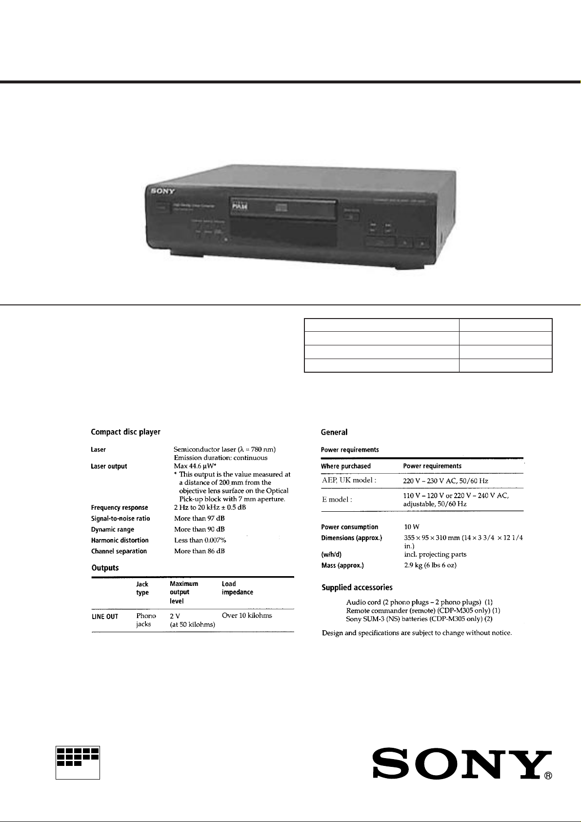
Photo : CDP-M305
Model Name Using Similar Machanism CDP-M201/M301
CD Mechanism Type CDM14-5BD29B
Base Unit Type BU-5BD29B
Optical Pick-up Type KSS-213B/K-N
SPECIFICATIONS
MICROFILM
COMPACT DISC PLAYER
TABLE OF CONTENTS
Specifications ........................................................................... 1
WARNING
To prevent fire or shock hazard, do
not expose the unit to rain on
moisture.
To avoid electrical shock, do not
open the cabinet. Refer servicing to
qualified personnel only.
Laser component in this product is capable of emitting radiation
exceeding the limit for Class 1.
This appliance is classified as a
CLASS 1 LASER product.
The CLASS 1 LASER
PRODUCT MARKING is
located on the rear exterior.
The following caution label is
located inside of the unit.
1. GENERAL
Location and Function of Controls .................................... 3
2. SERVICING NOTE .......................................................... 4
3. DISASSEMBLY ............................................................... 5
4. ELECTRICAL ADJUSTMENTS ................................... 6
5. DIAGRAMS
5-1. IC Pin Function........................................................... 7
5-2. Printed Wiring Boards – BD Section – ...................... 11
5-3. Schematic Diagram – BD Section – ......................... 13
5-4. Schematic Diagram – Main Section – ...................... 17
5-5. Printed Wiring Boards – Main Section –.................. 21
6. EXPLODED VIEWS
6-1. Main Section............................................................. 26
6-2. CD Block Section ..................................................... 27
6-3. Optical Pick-up Block Section (BU-5BD29B)......... 28
7. ELECTRICAL PARTS LIST ........................................ 29
MODEL IDENTIFICATION
COMPACT DISC PLAYER
SERIAL NO.
MADE IN JAPAN
AEP, UK model :
AC : 220–230V
E model :
AC : 110–120V, 220–240V
MODEL NO.
⁄50/60Hz 10W
CDP-M205
CDP-M305
⁄ Adjustable 50/60Hz 10W
SAFETY-RELATED COMPONENT WARNING!!
COMPONENTS IDENTIFIED BY MARK
MARK
! ON THE SCHEMATIC DIAGRAMS AND IN THE PARTS
LIST ARE CRITICAL TO SAFE OPERATION.
REPLACE THESE COMPONENTS WITH SONY PARTS WHOSE
PART NUMBERS APPEAR AS SHOWN IN THIS MANUAL OR IN
SUPPLEMENTS PUBLISHED BY SONY.
! OR DO TTED LINE WITH
– 2 –
LOCATION AND FUNCTION OF CONTROLS
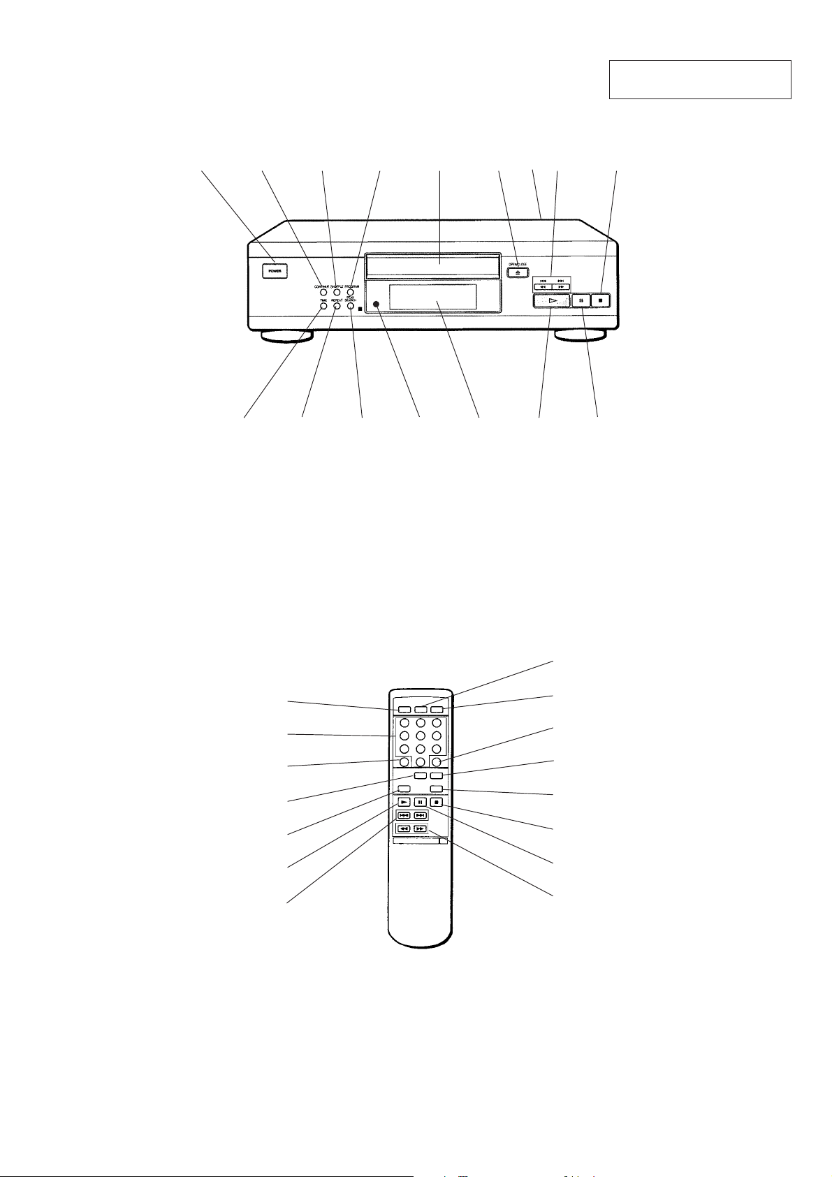
Front Panel
123456!§78
!∞ !¢ !£ !™ !¡ 0 9
SECTION 1
GENERAL
This section is extracted from
instruction manual.
1 POWER switch
2 CONTINUE button
3 SHUFFLE button
4 PROGRAM button
5 DISK tray
6 OPEN/CLOSE button
7 0/) (MANUAL SEARCH) buttons
=/+(AMS : AUTOMATIC MUSIC SENSOR) buttons
8 p(STOP) button
Remote Commander (CDP-M305 only)
!∞
!¢
!£
!™
!¡
0
9 P(PAUSE) button
0 ·(PLAY) button
!¡ DISPLAY window
!™ REMOTE senser (CDP-M305 only)
!£ PEAK SEARCH button
!¢ REPEAT button
!∞ TIME button
!§ VOLTAGE selector (Singapore model)
1
2
3
4
5
6
7
9
1 SHUFFLE button
2 PROGRAM button
3 CLEAR button
4 CHECK button
5 FADER button
6 p(STOP) button
7 P(PAUSE) button
8 0/)(MANUAL SEARCH) buttons
8
9 =/+(AMS : AUTOMATIC MUSIC SENSOR) buttons
0 ((PLAY) button
!¡ REPEAT button
!™ TIME button
!£ >10 (OVER 10) button
!¢ NUMBER buttons
!∞ CONTINUE button
– 3 –
SECTION 2
SERVICING NOTE
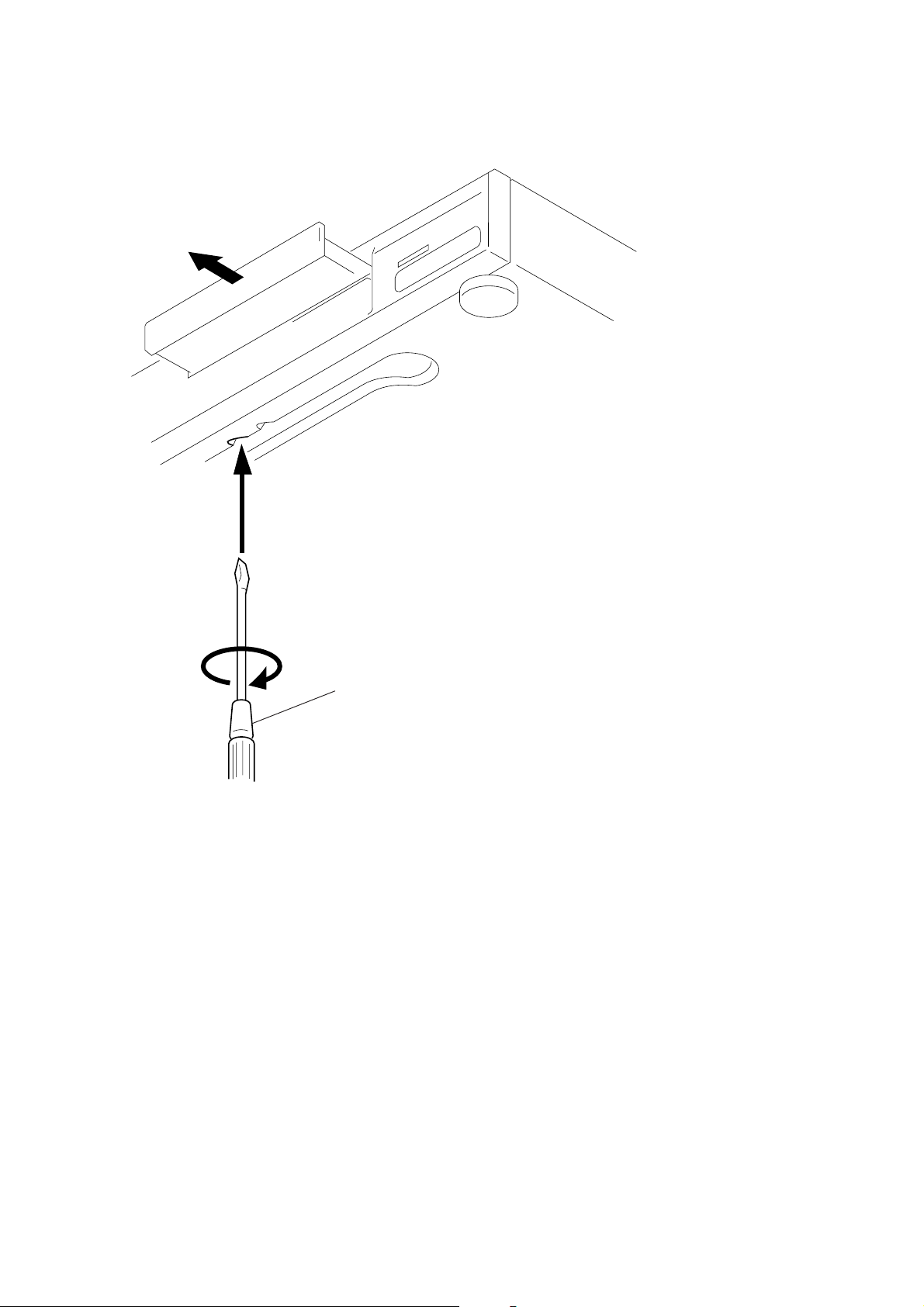
HOW TO OPEN THE DISC TRAY WHEN POWER SWITCH TURNS OFF
1
Turn in the direction of the arrow
Caution : When you work, keep the set horizontal.
– 4 –
SECTION 3
DISASSEMBLY
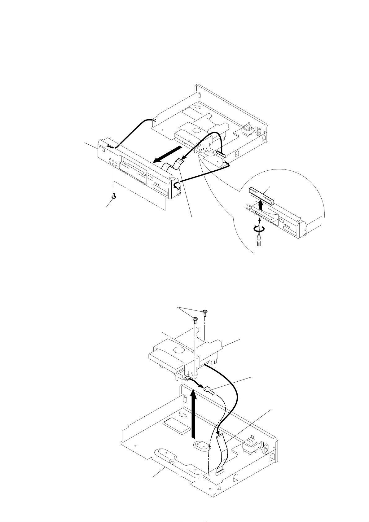
Note : Follow the disassembly procedure in the numerical order given.
3-1. PANEL, FRONT REMOVAL
5
Panel, Front
6
5
Panel, Loading
4
T wo screws
(+BVTP 3x8TYPE2 N-S)
3-2. CD MECHANISM SECTION REMOVAL
1
Three screws
(+BVTP 3x8 TYPE2 N-S)
3
Wire (Flat type)
(21core)
2
2
1
Turn in the direction
of the arrow
(Refer to page 4)
CD mechanism section
CN151 (5P)
3
Chassis assy
4
– 5 –
Wire (Flat type) (19 core)
SECTION 4
ELECTRICAL ADJUSTMENTS
CD SECTION
Note:
1. CD Block is basically constructed to operate without adjustment.
Therefore, check each item in order given.
2. Use YEDS-18 disc (3-702-101-01) unless otherwise indicated.
3. Use an oscilloscope with more than 10M impedance.
4. Clean the object lens by an applicator with neutral detergent when
the signal level is low than specified value with the following
checks.
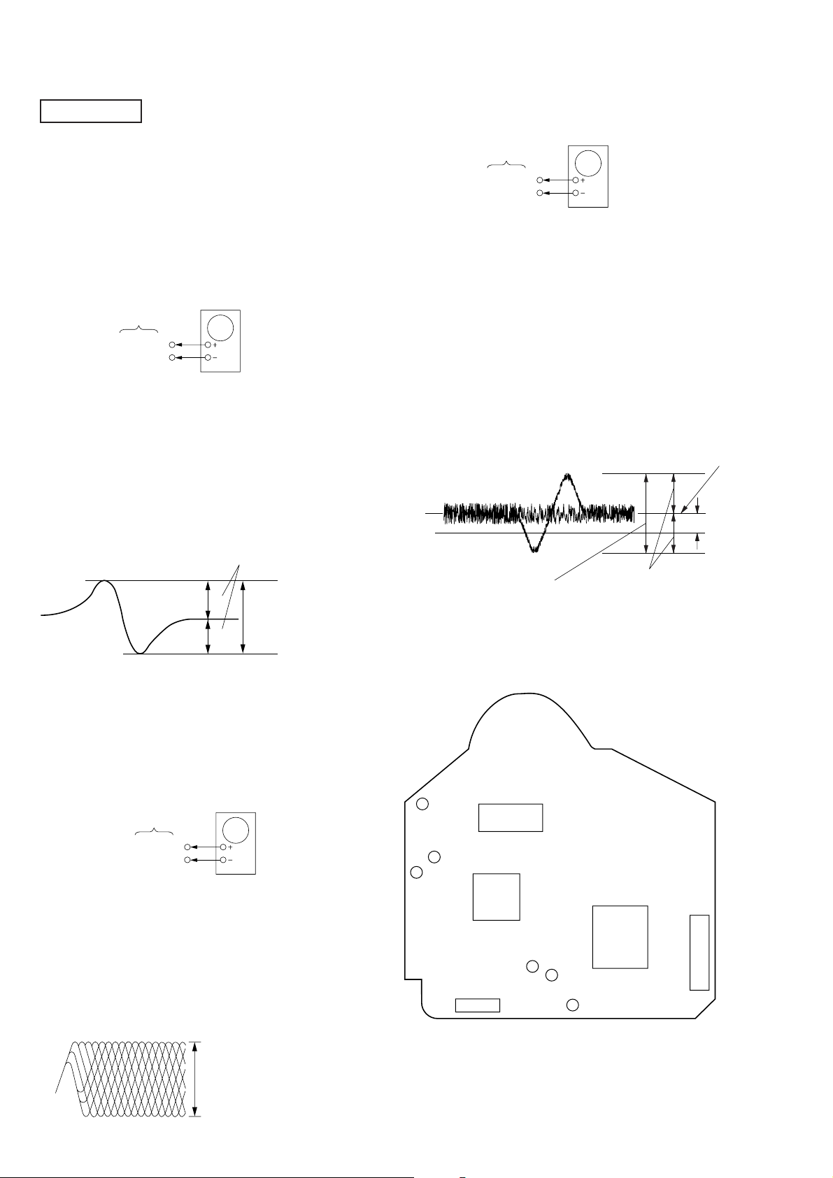
S Curve Check
oscilloscope
BD board
TP (FEO)
TP (VC)
Procedure :
1. Connect oscilloscope to test point TP (FEO).
2. Connect between test point TP (FOK) and Ground by lead wire.
3. Turn Power switch on.
4. Put disc (YEDS-18) in and turned Power switch on again and
actuate the focus search. (actuate the focus search when disc
table is moving in and out.)
5. Check the oscilloscope waveform (S-curve) is symmetrical between A and B. And confirm peak to peak le vel within 3 ± 1Vp-p.
S-curve waveform
symmetry
E-F Balance (1 Track Jump) check
oscilloscope
BD board
TP (TEO)
TP (VC)
Procedure:
1. Connect oscilloscope to test point TP (TEO) on BD board.
2. Turned Power switch on.
3. Put disc (YEDS-18) in to play the number five track.
4. Press the “P (Pause)” button.
5. Check the level B of the oscilloscope's wa veform and the A (DC
voltage) of the center of the Tr averse waveform.
Confirm the following:
• A/B x 100 = less than ± 7 (%)
1 track jump waveform
Center of the waveform
B
A (DC voitage)
0V
A
within 3 ± 1 Vp-p
B
6. After check, remove the lead wire connected in step 2.
Note: • T ry to measure sev eral times to make sure than the ratio of
A : B or B : A is more than 10 : 7.
• Take sweep time as long as possible and light up the brightness to obtain best waveform.
RF Level Check
oscilloscope
BD board
TP (RF)
TP (VC)
Procedure :
1. Connect oscilloscope to test point TP (RF) on BD board.
2. Turned Power switch on.
3. Put disc (YEDS-18) in and playback.
4. Confirm that oscilloscope waveform is clear and check RF signal level is correct or not.
Note: Clear RF signal waveform means that the shape “◊” can be
clearly distinguished at the center of the waveform.
RF signal waveform
VOLT/DIV: 200 mV
TIME/DIV: 500 nS
level : 500 mV ± 100 mVp-p
Adjustment Location:
[BD BOARD] (Conductor Side)
TP
(VC)
TP
(FOK)
TP
(RF)
CNU101
IC102
IC101
TP
(TEO)
TP
(FEO)
Symmetry
IC103
CNU102
TP
(GND)
level: 1.1 ± 0.3 Vp-p
– 6 –

SECTION 5
DIAGRAMS
5-1. IC PIN FUNCTION
IC101 FOCUS/TRACKING/SLED SERVO RF AMP (CXA1992AR)
Pin No. Pin name I/O Description.
1 FEO O
2 FEI I Focus error input.
3 FDFCT I Capacitor connection pin for defect time constant.
4 FGD I Ground this pin through a capacitor for cutting the focus servo high-frequency gain.
5 FLB I External time constant setting pin for boosting the focus servo low-frequency.
6 FE O O Focus drive output.
7 FE M I Focus amplifier inverted input.
8 SRCH I External time constant setting pin for generating focus search waveform.
9 TGU I External time constant setting pin for switching tracking high-frequency gain.
10 TG2 I External time constant setting pin for switching tracking high-frequency gain.
11 FSET I Peak frequency setting pin for focus and tracking phase compensation amplifier.
12 TA M I Tracking amplifier inverted input.
13 TA O O Tracking drive output.
14 SL P I Sled amplifier non-inverted input.
15 SL M I Sled amplifier inverted input.
16 SL O O Sled drive output.
17 ISET I
18 VCC I Positive power supply.
19 LOCK I The sled overrun prevention circuit operates when this pin is Low (No pull-up resistance).
20 CLK I Serial data transfer clock input from CPU (No pull-up resistance).
21 XLT I Lach input from CPU (No pull-up resistance).
22 DATA I Serial data input from CPU (No pull-up resistance).
23 XRST I Reset input; resets at Low (No pull-up resistance).
24 C.OUT O Track number count signal output.
25 SENS1 O
26 SENS2 O
27 FOK O Focus OK comparator output.
28 CC2 I Input for the defect bottom hold output with capacitance coupled.
29 CC1 O
30 CB I Connection pin for defect bottom hold capacitor.
31 CP I
32 RF I I Input for the RF summing amplifier output with capacitance coupled.
33 RF O O
34 RF M I
35 RFTC I External time constant setting pin during RF level control.
36 LD O APC amplifier output.
37 PD I APC amplifier input.
38 PD1 I RF I-V amplifier inverted input.
39 PD2 I Connect these pins to the photo diode A+C and B+D pins.
40 FE BIAS I
Focus error amplifier output.
Connected internally to the window comparator input for bias adjustment.
Connect an external capacitance to set the current which determines the Focus search,
Track jump, and Sled kick heights.
Outputs FZC, DFCT1, TZC, BALH, TGH, FOH, ATSC, and others according to the
command from CPU.
Outputs DFCT2, MIRR, BALL, TGL, FOL,and others according to the command from
CPU.
Defect bottom hold output
Connected internally to the interruption comparator input.
Connection pin for MIRR hold capacitor
MIRR comparator non-inverted input.
RF summing amplifier output
Eye-pattern check point.
RF summing amplifier inverted input.
The RF amplifier gain is determined by the resistance connected between this pin and
RFO pin .
Bias adjustment of focus error amplifier
Leave this pin open for automatic adjustment (not used).
– 7 –
 Loading...