

Siemens SAB-C502-2R20N, SAB-C502-2R20P, SAB-C502-2RN, SAB-C502-2RP, SAB-C502-L20N Datasheet
...
Data Sheet 08.94
Microcomputer Components
C502
8-Bit CMOS Microcontroller
http://www.siemens.de/
Semiconductor/
Semiconductor Group 1 08.94
8-Bit CMOS Microcontroller
Preliminary
C502
●
Fully compatible to standard 8051 microcontroller
●
Versions for 12 / 20 MHz operating frequency
● 16 K × 8 ROM (SAB-C502-2R only)
●
256 × 8 RAM
●
256 × 8 XRAM (additional on-chip RAM)
●
Eight datapointers for indirect addressing of program and external data memory
(including XRAM)
●
Four 8-bit ports
●
Three 16 -bit Timers / Counters (Timer 2 with Up/Down Counter feature)
● USART with programmable 10-bit Baudrate-Generator
●
Six interrupt sources, two priority levels
●
Programmable 15-bit Watchdog Timer
●
Oscillator Watchdog
●
Fast Power On Reset
●
Power Saving Modes
●
P-DIP-40 package and P-LCC-44 package
● Temperature ranges: SAB-C502
T
A
: 0 ˚C to 70 ˚C
SAF-C502
T
A
: – 40 ˚C to 85 ˚C
SAB-C502

Semiconductor Group 2
C502
The SAB-C502-L/C502-2R described in this document is compatible with the SAB 80C52 and can
be used for all present SAB 80C52 applications.
The SAB-C502-2R contains a non-volatile 16 K × 8 read-only program memory, a volatile 256 × 8
read/write data memory, four ports, three 16-bit timers/counters, a six source, two priority level
interrupt structure, a serial port and versatile fail save mechanisms. The SAB-C502-L/C502-2R
incorporates 256 × 8 additional on-chip RAM called XRAM. For higher performance eight
datapointers are implemented. The SAB-C502-L is identical, except that it lacks the program
memory on chip. Therefore the term SAB-C502 refers to both versions within this specification
unless otherwise noted.

Semiconductor Group 3
C502
Ordering Information
Note:Extended temperature range – 40 ˚C to 110 ˚C (SAH-C502) on request.
Type Ordering
Code
Package Description
(8-Bit CMOS microcontroller)
SAB-C502-LN
SAB-C502-LP
Q67120-C838
Q67120-C889
P-LCC-44
P-DIP-40
for external memory 12 MHz
SAB-C502-2RN
SAB-C502-2RP
Q67120-C839
Q67120-C890
P-LCC-44
P-DIP-40
with mask-programmable ROM,
12 MHz
SAB-C502-L20N
SAB-C502-L20P
Q67120-C885
Q67120-C891
P-LCC-44
P-DIP-40
for external memory 20 MHz
SAB-C502-2R20N
SAB-C502-2R20P
Q67120-C884
Q67120-C892
P-LCC-44
P-DIP-40
with mask-programmable ROM,
20 MHz
SAF-C502-LN
SAF-C502-LP
Q67120-C883
Q67120-C893
P-LCC-44
P-DIP-40
for external ROM, 12 MHz,
ext. temp. – 40 ˚C to 85 ˚C
SAF-C502-2RN
SAF-C502-2RP
Q67120-C886
Q67120-C894
P-LCC-44
P-DIP-40
with mask-programmable ROM,
12 MHz, ext. temp. – 40 ˚C to 85 ˚C
SAF-C502-L20N
SAF-C502-L20P
Q67120-C887
Q67120-C895
P-LCC-44
P-DIP-40
for external memory, 20 MHz,
ext. temp. – 40 ˚C to 85 ˚C
SAF-C502-2R20N
SAF-C502-2R20P
Q67120-C888
Q67120-C896
P-LCC-44
P-DIP-40
with mask-programmable ROM,
20 MHz, ext. temp. – 40 ˚C to 85 ˚C
Semiconductor Group 4
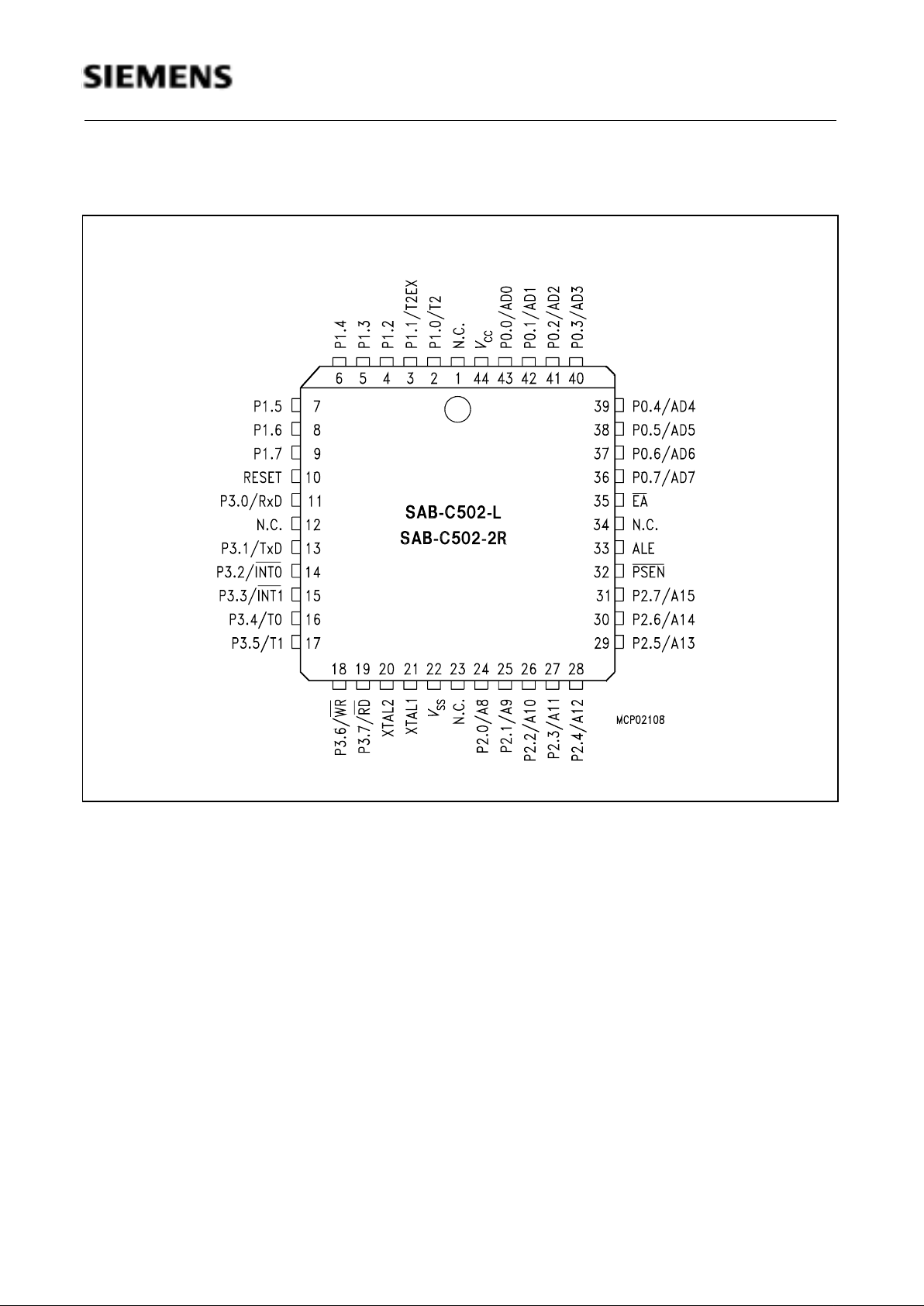
Pin Configuration
(top view)
(P-LCC-44)
C502
Semiconductor Group 5
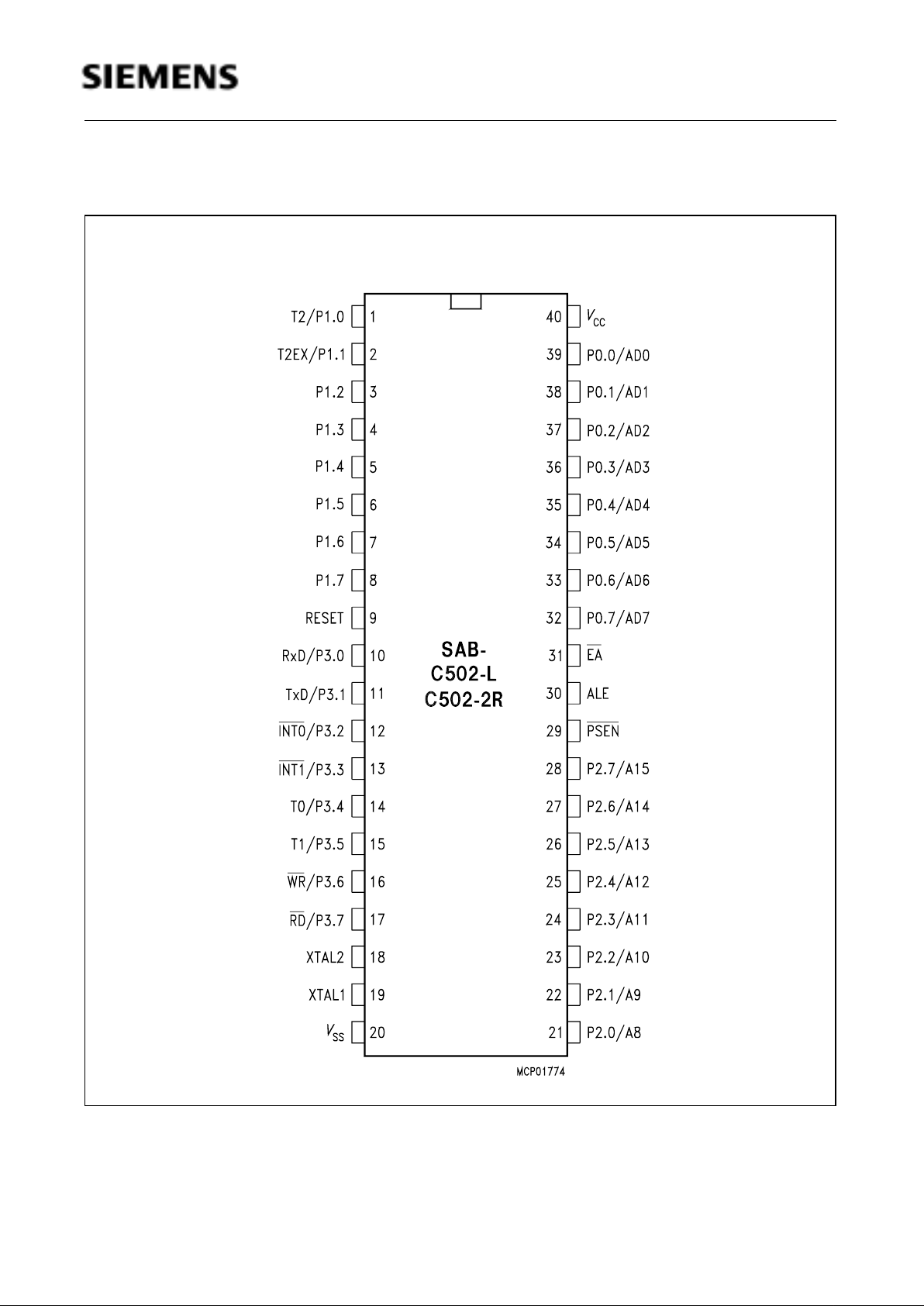
C502
Pin Configuration
(top view)
(P-DIP-40)

Semiconductor Group 6
Logic Symbol
C502

Semiconductor Group 7
C502
Pin Definitions and Functions
Symbol Pin Number I/O*) Function
P-LCC-44 P-DIP-40
P1.7 – P1.0 9–2
2
3
8–1
1
2
I Port 1
is a bidirectional I/O port with internal pull-up
resistors. Port 1 pins that have 1s written to
them are pulled high by the internal pull-up
resistors, and in that state can be used as
inputs. As inputs, port 1 pins being externally
pulled low will source current (
I
IL
, in the DC
characteristics) because of the internal pull-up
resistors. Port 1 also contains the timer 2 pins
as secondary function. The output latch corresponding to a secondary function must be programmed to a one (1) for that function to
operate.
The secondary functions are assigned to the
pins of port 1, as follows:
P1.0 T2 Input to counter 2
P1.1 T2EX Capture - Reload trigger of
timer 2 / Up-Down count
*) I = Input
O = Output
Semiconductor Group 8
P3.0 – P3.7 11, 13–19
11
13
14
15
16
17
18
19
10–17
10
11
12
13
14
15
16
17
I/O Port 3
is a bidirectional I/O port with internal pull-up
resistors. Port 3 pins that have 1s written to
them are pulled high by the internal pull-up
resistors, and in that state can be used as
inputs. As inputs, port 3 pins being externally
pulled low will source current (I
IL
, in the DC
characteristics) because of the internal pull-up
resistors. Port 3 also contains the interrupt,
timer, serial port 0 and external memory strobe
pins that are used by various options. The output latch corresponding to a secondary function must be programmed to a one (1) for that
function to operate.
The secondary functions are assigned to the
pins of port 3, as follows:
P3.0 R×D receiver data input
(asynchronous) or data input/
output (synchronous) of serial
interface 0
P3.1 T×D transmitter data output
(asynchronous) or clock output
(synchronous) of the serial
interface 0
P3.2 INT0
interrupt 0 input/timer 0 gate
control
P3.3 INT1 interrupt 1 input/timer 1 gate
control
P3.4 T0 counter 0 input
P3.5 T1 counter 1 input
P3.6 WR the write control signal latches
the data byte from port 0 into the
external data memory
P3.7 RD the read control signal enables
the external data memory to
port 0
XTAL2 20 18 – XTAL2
Output of the inverting oscillator amplifier
*)I = Input
O = Output
Pin Definitions and Functions (cont’d)
Symbol Pin Number I/O*) Function
P-LCC-44 P-DIP-40
C502

Semiconductor Group 9
C502
XTAL1 21 19 – XTAL1
Input to the inverting oscillator amplifier and
input to the internal clock generator circuits.
To drive the device from an external clock
source, XTAL1 should be driven, while XTAL2
is left unconnected. There are no requirements
on the duty cycle of the external clock signal,
since the input to the internal clocking circuitry
is divided down by a divide-by-two flip-flop.
Minimum and maximum high and low times as
well as rise fall times specified in the AC
characteristics must be observed.
P2.0 – P2.7 24–31 21–28 I/O Port 2
ia a bidirectional I/O port with internal pull-up
resistors. Port 2 pins that have 1s written to
them are pulled high by the internal pull-up
resistors, and in that state can be used as
inputs. As inputs, port 2 pins being externally
pulled low will source current (
I
IL
, in the DC
characteristics) because of the internal pull-up
resistors. Port 2 emits the high-order address
byte during fetches from external program
memory and during accesses to external data
memory that use 16-bit addresses (MOVX
@DPTR). In this application it uses strong
internal pull-up resistors when issuing 1s.
During accesses to external data memory that
use 8-bit addresses (MOVX @Ri), port 2
issues the contents of the P2 special function
register.
PSEN
32 29 O The Program Store Enable
output is a control signal that enables the
external program memory to the bus during
external fetch operations. It is activated every
six oscillator periodes except during external
data memory accesses. Remains high during
internal program execution.
*) I = Input
O = Output
Pin Definitions and Functions (cont’d)
Symbol Pin Number I/O*) Function
P-LCC-44 P-DIP-40

Semiconductor Group 10
RESET 10 9 I RESET
A high level on this pin for two machine cycles
while the oscillator is running resets the
device. An internal diffused resistor to V
SS
permits power-on reset using only an external
capacitor to
V
CC
.
ALE 33 30 O The Address Latch Enable
output is used for latching the low-byte of the
address into external memory during normal
operation. It is activated every six oscillator
periodes except during an external data
memory access.
EA
35 31 I External Access Enable
When held at high level, instructions are
fetched from the internal ROM (SAB-C502-2R
only) when the PC is less than 4000H. When
held at low level, the SAB-C502 fetches all
instructions from external program memory.
For the SAB-C502-L this pin must be tied low.
P0.0 – P0.7 43–36 39–32 I/O Port 0
is an 8-bit open-drain bidirectional I/O port.
Port 0 pins that have 1s written to them float,
and in that state can be used as highimpedance inputs. Port 0 is also the
multiplexed low-order address and data bus
during accesses to external program or data
memory. In this application it uses strong
internal pull-up resistors when issuing 1s.
Port 0 also outputs the code bytes during
program verification in the SAB-C502-2R.
External pull-up resistors are required during
program verification.
V
SS
22 20 – Circuit ground potential
V
CC
44 40 – Supply terminal for all operating modes
N.C. 1, 12,
23, 34
––No connection
*) I = Input
O = Output
Pin Definitions and Functions (cont’d)
Symbol Pin Number I/O*) Function
P-LCC-44 P-DIP-40
C502

Semiconductor Group 11
C502
Functional Description
The SAB-C502 is fully compatible to the standard 8051 microcontroller family.
It is compatible with the SAB 80C52. While maintaining all architectural and operational
characteristics of the SAB 80C52 the SAB-C502 incorporates some enhancements in the Timer2
and Fail Save Mechanism Unit.
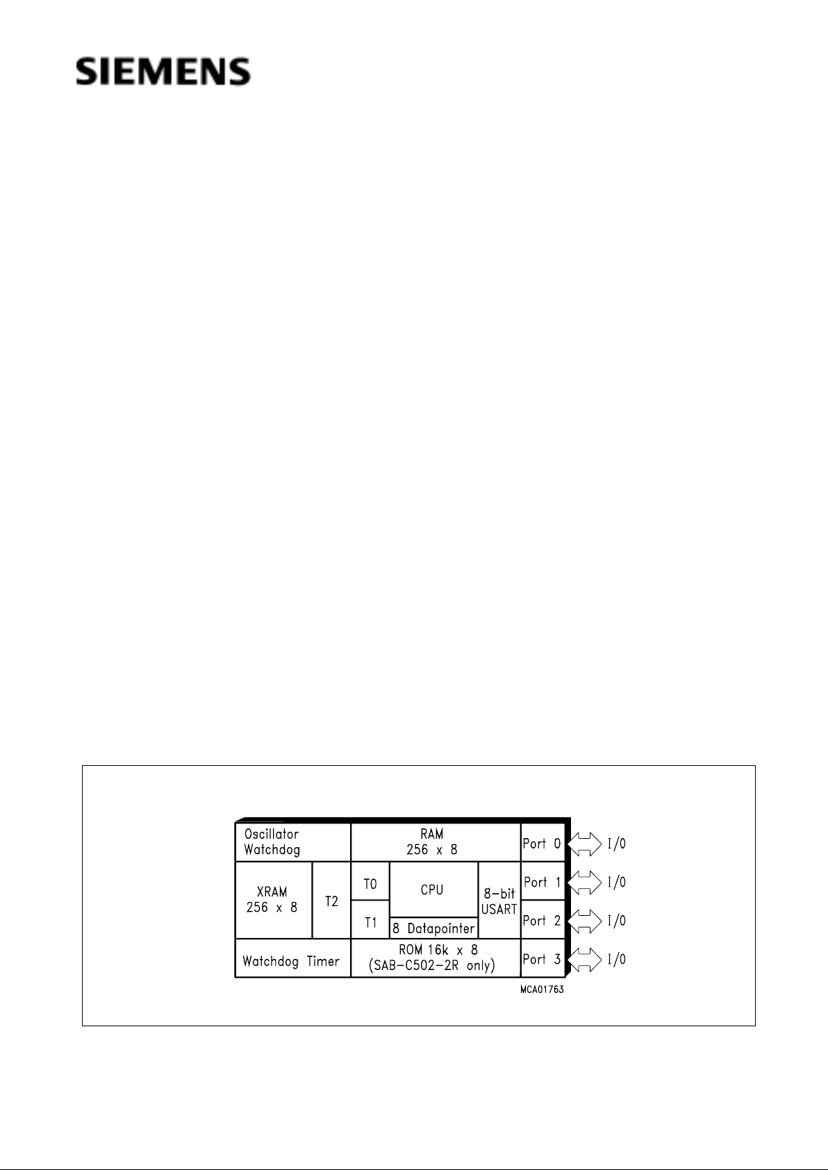
Figure 1 shows a block diagram of the SAB-C502.
Figure 1
Block Diagram of the SAB-C502

Semiconductor Group 12
CPU
The SAB-C502 is efficient both as a controller and as an arithmetic processor. It has extensive
facilities for binary and BCD arithmetic and excels in its bit-handling capabilities. Efficient use of
program memory results from an instruction set consisting of 44 % one-byte, 41 % two-byte, and
15 % three-byte instructions. With a 12 MHz crystal, 58 % of the instructions execute in 1.0 µs
(18 MHz : 667 ns).
Special Function Register PSW
Reset value of PSW is 00H.
Bit Function
CY Carry Flag
AC Auxiliary Carry Flag (for BCD operations)
F0 General Purpose Flag
RS1 RS0
00
01
10
11
Register Bank select control bits
Bank 0 selected, data address 00H - 07
H
Bank 1 selected, data address 08H - 0F
H
Bank 2 selected, data address 10H - 17
H
Bank 3 selected, data address 18H - 1F
H
OV Overflow Flag
F1 General Purpose Flag
P Parity Flag.
Set/cleared by hardware each instruction cycle to indicate an odd/
even number of “one” bits in the accumulator, i.e. even parity.
CY AC F0 RS1 RS0 OV F1 P
MSB LSB
76543210
Addr. D0
H
PSW
Bit No.
C502

Semiconductor Group 13
C502
Special Function Registers
All registers, except the program counter and the four general purpose register banks, reside in the
special function register area.
The 36 special function register (SFR) include pointers and registers that provide an interface
between the CPU and the other on-chip peripherals. There are also 128 directly addressable bits
within the SFR area.
All SFRs are listed in table 1, table 2 and table 3. In table 1 they are organized in numeric order
of their addresses. In table 2 they are organized in groups which refer to the functional blocks of the
SAB-C502. Table 3 illustrates the contents of the SFRs.
Table 1
Special Function Register in Numeric Order of their Addresses
1)
: Bit-addressable Special Function Register
2)
: X means that the value is indeterminate and the location is reserved
Address Register Contents
after Reset
Address Register Contents
after Reset
80
H
81
H
82
H
83
H
84
H
85
H
86
H
87
H
P0
1)
SP
DPL
DPH
reserved
reserved
WDTREL
PCON
FF
H
07
H
00
H
00
H
00
H
000X0000
B
2)
98
H
99
H
9A
H
9B
H
9C
H
9D
H
9E
H
9F
H
SCON
1)
SBUF
reserved
reserved
reserved
reserved
reserved
reserved
00
H
XX
H
2)
XX
H
2)
XX
H
2)
XX
H
2)
XX
H
2)
XX
H
2)
XX
H
2)
88
H
89
H
8A
H
8B
H
8C
H
8D
H
8E
H
8F
H
TCON
1)
TMOD
TL0
TL1
TH0
TH1
reserved
reserved
00
H
00
H
00
H
00
H
00
H
00
H
XX
H
2)
XX
H
2)
A0
H
A1
H
A2
H
A3
H
A4
H
A5
H
A6
H
A7
H
P2
1)
reserved
reserved
reserved
reserved
reserved
reserved
reserved
FF
H
XX
H
2)
XX
H
2)
XX
H
2)
XX
H
2)
XX
H
2)
XX
H
2)
XX
H
2)
90
H
91
H
92
H
93
H
94
H
95
H
96
H
97
H
P1
1)
XPAGE
DPSEL
reserved
XCON
reserved
reserved
reserved
FF
H
00
H
XXXXX000
B
2)
XX
H
2)
F8
H
XX
H
2)
XX
H
2)
XX
H
2)
A8
H
A9
H
AA
H
AB
H
AC
H
AD
H
AE
H
AF
H
IE
1)
reserved
SRELL
reserved
reserved
reserved
reserved
reserved
0X000000
B
2)
XX
H
2)
D9
H
XX
H
2)
XX
H
2)
XX
H
2)
XX
H
2)
XX
H
2)

Semiconductor Group 14
Table 1
Special Function Register in Numeric Order of their Addresses (cont’d)
1)
: Bit-addressable Special Function Register
2)
: X means that the value is indeterminate and the location is reserved
Address Register Contents
after Reset
Address Register Contents
after Reset
B0
H
B1
H
B2
H
B3
H
B4
H
B5
H
N6
H
B7
H
P3
1)
SYSCON
reserved
reserved
reserved
reserved
reserved
reserved
FF
H
XXXXXX01
B
2)
XX
H
2)
XX
H
2)
XX
H
2)
XX
H
2)
XX
H
2)
XX
H
2)
D8
H
D9
H
DA
H
DB
H
DC
H
DD
H
DE
H
DF
H
BAUD
reserved
reserved
reserved
reserved
reserved
reserved
reserved
0XXXXXXX
B
2)
XX
H
2)
XX
H
2)
XX
H
2)
XX
H
2)
XX
H
2)
XX
H
2)
XX
H
2)
B8
H
B9
H
BA
H
BB
H
BC
H
BD
H
BE
H
BF
H
IP
1)
reserved
SRELH
reserved
reserved
reserved
reserved
reserved
X0000000
B
2)
XX
H
2)
XXXXXX11
B
2)
XX
H
2)
XX
H
2)
XX
H
2)
XX
H
2)
XX
H
2)
E0
H
E1
H
E2
H
E3
H
E4
H
E5
H
E6
H
E7
H
ACC
1)
reserved
reserved
reserved
reserved
reserved
reserved
reserved
00
H
XX
H
2)
XX
H
2)
XX
H
2)
XX
H
2)
XX
H
2)
XX
H
2)
XX
H
2)
C0
H
C1
H
C2
H
C3
H
C4
H
C5
H
C6
H
C7
H
WDCON
1)
reserved
reserved
reserved
reserved
reserved
reserved
reserved
XXXX0000
B
2)
XX
H
2)
XX
H
2)
XX
H
2)
XX
H
2)
XX
H
2)
XX
H
2)
XX
H
2)
E8
H
E9
H
EA
H
EB
H
EC
H
ED
H
EE
H
EF
H
reserved
reserved
reserved
reserved
reserved
reserved
reserved
reserved
XX
H
2)
XX
H
2)
XX
H
2)
XX
H
2)
XX
H
2)
XX
H
2)
XX
H
2)
XX
H
2)
C8
H
C9
H
CA
H
CB
H
CC
H
CD
H
CE
H
CF
H
T2CON
1)
T2MOD
RC2L
RC2H
TL2
TH2
reserved
reserved
00
H
XXXXXXX0
B
2)
00
H
00
H
00
H
00
H
XX
H
2)
XX
H
2)
F0
H
F1
H
F2
H
F3
H
F4
H
F5
H
F6
H
F7
H
B
1)
reserved
reserved
reserved
reserved
reserved
reserved
reserved
00
H
XX
H
2)
XX
H
2)
XX
H
2)
XX
H
2)
XX
H
2)
XX
H
2)
XX
H
2)
D0
H
D1
H
D2
H
D3
H
D4
H
D5
H
D6
H
D7
H
PSW
1)
reserved
reserved
reserved
reserved
reserved
reserved
reserved
00
H
XX
H
2)
XX
H
2)
XX
H
2)
XX
H
2)
XX
H
2)
XX
H
2)
XX
H
2)
F8
H
F9
H
FA
H
FB
H
FC
H
FD
H
FE
H
FF
H
reserved
reserved
reserved
reserved
reserved
reserved
reserved
reserved
XX
H
2)
XX
H
2)
XX
H
2)
XX
H
2)
XX
H
2)
XX
H
2)
XX
H
2)
XX
H
2)
C502

Semiconductor Group 15
C502
Table 2
Special Function Registers - Functional Blocks
1)
: Bit-addressable special function registers
2)
: This special function register is listed repeatedly since some bits of it also belong to other functional blocks.
3)
: X means that the value is indeterminate and the location is reserved
Block Symbol Name Address Contents
after Reset
CPU ACC
B
DPH
DPL
DPSEL
PSW
SP
Accumulator
B-Register
Data Pointer, High Byte
Data Pointer, Low Byte
Data pointer select register
Program Status Word Register
Stack Pointer
E0
H
1)
F0
H
1)
83
H
82
H
92
H
D0
H
1)
81
H
00
H
00
H
00
H
00
H
XXXX X000
B
3)
00
H
07
H
Interrupt
System
IE
IP
Interrupt Enable Register
Interrupt Priority Register
A8
H
1)
B8
H
1)
0X00 0000
B
3)
X000 0000
B
3)
Ports P0
P1
P2
P3
Port 0
Port 1
Port 2
Port 3
80
H
1)
90
H
1)
A0
H
1)
B0
H
1)
FF
H
FF
H
FF
H
FF
H
XRAM XPAGE
XCON
SYSCON
Page addr. reg. for XRAM
XRAM startaddress (highbyte)
XRAM control register
91
H
94
H
B1
H
00
H
F8
H
XXXX XX01
B
3)
Serial
Channels
PCON
2)
SBUF
SCON
SRELL
SRELH
BAUD
Power Control Register
Serial Channel Buffer Reg.
Serial Channel Control Reg.
Baudrate Generator Reloadvalue, Lowbyte
Baudrate Generator Reloadvalue, Highbyte
Baudrate Generator Enable Bit
87
H
99
H
98
H
1)
AA
H
BA
H
D8
H
1)
00
H
XX
H
3)
00
H
D9
H
XXXX XX11
B
3)
0XXX XXXX
B
3)
Timer 0/
Timer 1
TCON
TH0
TH1
TL0
TL1
TMOD
Timer 0/1 Control Register
Timer 0, High Byte
Timer 1, High Byte
Timer 0, Low Byte
Timer 1, Low Byte
Timer Mode Register
88
H
1)
8C
H
8D
H
8A
H
8B
H
89
H
00
H
00
H
00
H
00
H
00
H
00
H
Timer 2 T2CON
T2MOD
RC2L
RC2H
TH2
TL2
Timer 2 Control Register
Timer 2 Mode Register
Timer 2, Reload Capture Register, Low Byte
Timer 2, Reload Capture Register, High Byte
Timer 2, High Byte
Timer 2, Low Byte
C8
H
1)
C9
H
CA
H
CB
H
CD
H
CC
H
00
H
XXXX XXX0
B
3)
00
H
00
H
00
H
00
H
Watchdog WDCON
WDTREL
Watchdog Timer Control Register
Watchdog Timer Reload Reg.
C0
H
1)
86
H
XXXX 0000
B
3)
00
H
Pow. Sav.
Modes
PCON
2)
Power Control Register 87
H
000X 0000
B
3)

Semiconductor Group 16
Table 3
Contents of SFR’s, SFR’s in Numeric Order
Address Register
80
H
P0
82
H
DPL
83
H
DPH
87
H
PCON
88
H
TCON
89
H
TMOD
8A
H
TL0
8B
H
TL1
8D
H
TH1
81
H
SP
8C
H
TH0
90
H
P1
91
H
XPAGE
92
H
DPSEL
94
H
XCON
98
H
SCON
99
H
SBUF
A8
H
IE
A0
H
P2
AA
H
SRELL
Bit 7 6 5 4 3 2 1 0
SMOD PDS IDLS – GF1 GF0 PDE IDLE
TF1 TR1 TF0 TR0 IE1 IT1 IE0 IT0
GATE C/T M1 M0 GATE C/T M1 M0
SM0 SM1 SM2 REN TB8 RB8 TI RI
– – – – – .2 .1 .0
EA – ET2 ES ET1 EX1 ET0 EX0
bit and byte addressable
not bit addressable
– = reserved
86
H
WDTREL
C502

Semiconductor Group 17
C502
Table 3
Contents of SFRs, SFRs in Numeric Order (cont’d)
Address Register
B0
H
P3
B8
H
IP
BA
H
SRELH
C8
H
T2CON
C9
H
T2MOD
CA
H
RC2L
CB
H
RC2H
CC
H
TL2
D0
H
PSW
B1
H
SYSCON
CD
H
TH2
D8
H
BAUD
E0
H
ACC
F0
H
B
Bit 7 6 5 4 3 2 1 0
TF2 EXF2 RCLK TCLK EXEN2 TR2 C/T2
CP/RL2
– – – – – – – DCEN
BD – – – – – – –
C0
H
WDCON
– – – – – – XMAP1 XMAP0
– PADC PT2 PS PT1 PX1 PT0 PX0
– – – – OWDS WDTS WDT SWDT
CY AC F0 RS1 RS0 OV F1 P
bit and byte addressable
not bit addressable
– = reserved

Semiconductor Group 18
Timer/Counter 0 and 1
Timer/Counter 0 and 1 can be used in four operating modes as listed in table 4:
Table 4
Timer/Counter 0 and 1 Operating Modes
In “timer” function (C/T = ‘0’) the register is incremented every machine cycle. Therefore the count
rate is f
OSC
/12.
In “counter” function the register is incremented in response to a 1-to-0 transition at its
corresponding external input pin (P3.4/T0, P3.5/T1). Since it takes two machine cycles to detect a
falling edge the max. count rate is f
OSC
/24. External inputs INT0 and INT1 (P3.2, P3.3) can be
programmed to function as a gate to facilitate pulse width measurements. Figure 2 illustrates the
input clock logic.
Figure 2
Timer/Counter 0 and 1 Input Clock Logic
Mode Description TMOD Input Clock
Gate C/T
M1 M0 internal external
(max)
0 8-bit timer/counter with a
divide-by-32 prescaler
XX00
f
OSC/12 × 32
f
OSC/24 × 32
1 16-bit timer/counter X X 0 1 f
OSC/12
f
OSC/24
2 8-bit timer/counter with
8-bit auto-reload
XX10f
OSC/12
f
OSC/24
3 Timer/counter 0 used as one
8-bit timer/counter and one
8-bit timer
Timer 1 stops
XX11f
OSC/12
f
OSC/24
C502

Semiconductor Group 19
C502
Timer 2
Timer 2 is a 16-bit Timer/Counter with up/down count feature. It can operate either as timer or as an
event counter which is selected by bit C/T2 (T2CON.1). It has three operating modes as shown in
table 5.
Table 5
Timer/Counter 2 Operating Modes
Note: ↓ = falling edge
Mode
T2CON T2MOD
DCEN
T2CON
EXEN
P1.1/
T2EX
Remarks
Input Clock
R×CLK
or
T×CLK
CP/
RL2
TR2 internal
external
(P1.0/T2)
16-bit
Autoreload
0
0
0
0
0
0
0
0
1
1
1
1
0
0
1
1
0
1
X
X
X
↓
0
1
reload upon
overflow
reload trigger
(falling edge)
Down counting
Up counting
f
OSC
/12
max
f
OSC
/24
16-bit
Capture
0
0
1
1
1
1
X
X
0
1
X
↓
16-bit Timer/
Counter (only
up-counting)
capture TH2,
TL2 → RC2H,
RC2L
f
OSC
/12
max
f
OSC
/24
Baud
Rate
Generator
1
1
X
X
1
1
X
X
0
1
X
↓
no overflow
interrupt
request (TF2)
extra external
interrupt
(“Timer 2”)
f
OSC
/2
max
f
OSC
/24
off X X 0 X X X Timer 2 stops – –

Semiconductor Group 20
Serial Interface (USART)
The serial port is full duplex and can operate in four modes (one synchronous mode, three
asynchronous modes) as illustrated in table 6. Figure 3 illustrates the block diagram of Baudrate
generation for the serial interface.
Table 6
USART Operating Modes
Figure 3
Block Diagram of Baud Rate Generation for Serial Interface
Mode
SCON Baudrate Description
SM0 SM1
000
f
OSC
/12 Serial data enters and exits through R×D.
T×D outputs the shift clock. 8-bit are
transmitted/received (LSB first)
1 0 1 Timer 1/2 overflow rate
or
Baudrate Generator
8-bit UART
10 bits are transmitted (through T×D) or
received (R×D)
210
f
OSC
/32 or f
OSC
/64 9-bit UART
11 bits are transmitted (T×D) or
received (R×D)
3 1 1 Timer 1/2 overflow rate
or
Baudrate Generator
9-bit UART
Like mode 2 except the variable
baud rate
C502

Semiconductor Group 21
C502
The possible baudrate can be calculated using the formulas given in table 7.
Table 7
Baudrates
The internal baudrate generator consists of a free running 10-bit timer with
f
OSC
/2 input frequency.
The internal baudrate generator is selected by setting bit BD in SFR BAUD.
Baud Rate
derived from
Interface Mode Baudrate
Oscillator 0
2
f
OSC
/12
(2
SMOD
× f
OSC
)/64
Timer 1 (16-bit timer)
(8-bit timer with
8-bit autoreload)
1,3
1,3
(2
SMOD
× timer 1 overflow rate)/32
(2
SMOD
× f
OSC
)/(32 × 12 × (256-TH1))
Timer 2 1,3
f
OSC
/(32 × (65536-(RC2H, RC2L))
Baudrate
Generator
1,3 (2
SMOD
× f
OSC
)/(64 × (210-SREL))

Semiconductor Group 22
Additional On-Chip RAM - XRAM
The SAB-C502 contains another 256byte of On-Chip RAM additional to the 256bytes internal RAM.
This RAM is called XRAM (‘eXtended RAM’) in this document.
The additional ON-Chip RAM is logically located in the external data memory range. The highbyte
of the XRAM address range startaddress is programmable by SFR XCON (94H). The reset value of
XCON is 0F8H (that is, XRAM address range F800HH … F8FFH).
The contents of the XRAM is not affected by a reset. After power up the contents is undefined, while
it remains unchanged during and after reset as long as the power supply is not turned off. The
XRAM is controlled by SFR SYSCON as shown in table 8.
Table 8
Control of the XRAM
Because of the XRAM is used in the same way as external data memory the same instruction types
must be used for accessing the XRAM. A general overview gives table 9.
Table 9
Accessing the XRAM
Note:When writing the page address (in page mode) at Port2 the value is also written in XPAGE.
However when writing XPAGE the value at PORT2 is not changed!
The behaviour of Port0/Port2 and RD
/WR during MOVX accesses is shown in table 10.
SFR SYSCON Description
XMAP1 XMAP0
0 1 Resetvalue. Access to XRAM is disabled. When cleared it can
be set again only by a reset
0 0 XRAM enabled
1 0 XRAM enabled. The signals RD
and WR are activated during
accesses to XRAM
Instruction
using
Instruction Remarks
DPTR MOVX A @DPTR
MOVX @ DPTR,A
Normally the use of these instructions would use a
physically external memory. However, in the SAB-C502
the XRAM is accessed if it is enabled.
R0/R1
(page mode)
MOVX A, @Ri
MOVX@Ri,A
Normally Port 2 serves as page register. However, the
distinction, whether Port 2 is as general purpose I/O or
as “page address” is made by the external design.
Hence a special SFR XPAGE is implemented the serve
the same function for the XRAM as Port 2 for external
data memory.
C502

Semiconductor Group 23
C502
Table 10
Behaviour of P0/P2 and RD/WR during MOVX Accesses
modes compatible to the standard 8051-family
EA = 0 EA = 1
XMAP1, XMAP0 XMAP1, XMAP0
00 10 X1 00 10 X1
MOVX
@DPTR
DPTR outside
XRAM address
range
(DPH ≠ XCON)
a) P0/P2 ➔ Bus
b) RD
/WR
active
c) ext. memory
is used
a) P0/P2 ➔ Bus
b) RD
/WR
active
c) ext. memory
is used
a) P0/P2 ➔ Bus
b) RD
/WR
active
c) ext. memory
is used
a) P0/P2 ➔ Bus
b) RD
/WR
active
c) ext. memory
is used
a) P0/P2 ➔ Bus
b) RD
/WR
active
c) ext. memory
is used
a) P0/P2 ➔ Bus
b) RD
/WR
active
c) ext. memory
is used
DPTR within
XRAM address
range
(DPH = XCON)
a) P0/P2 ➔ Bus
(WR
-Data only)
b) RD
/WR
inactive
c) XRAM is used
a) P0/P2 ➔ Bus
(WR
-Data only)
b) RD
/WR
active
c) XRAM is used
a) P0/P2 ➔ Bus
b) RD
/WR
active
c) ext. memory
is used
a) P0/P2 ➔ I/O
b) RD/WR
inactive
c) XRAM is used
a) P0/P2 ➔ Bus
(WR
-Data only)
b) RD
/WR
active
c) XRAM is used
a) P0/P2 ➔ Bus
b) RD
/WR
active
c) ext. memory
is used
MOVX
@Ri
XPAGE outside
XRAM addr. page
range
(XPAGE ≠ XCON)
a) P0 ➔ Bus
P2 ➔ I/O
b) RD
/WR
active
c) ext. memory
is used
a) P0 ➔ Bus
P2 ➔ I/O
b) RD
/WR
active
c) ext. memory
is used
a) P0 ➔ Bus
P2 ➔ I/O
b) RD
/WR
active
c) ext. memory
is used
a) P0 ➔ Bus
P2 ➔ I/O
b) RD
/WR
active
c) ext. memory
is used
a) P0 ➔ Bus
P2 ➔ I/O
b) RD
/WR
active
c) ext. memory
is used
a) P0 ➔ Bus
P2 ➔ I/O
b) RD
/WR
active
c) ext. memory
is used
XPAGE within
XRAM addr. page
range
(XPAGE = XCON)
a) P0 ➔ Bus
(WR
-Data only)
P2 ➔ I/O
b) RD
/WR
inactive
c) XRAM is used
a) P0 ➔ Bus
(WR
-Data only)
P2 ➔ I/O
b) RD
/WR
active
c) XRAM is used
a) P0 ➔ Bus
P2 ➔ I/O
b) RD
/WR
active
c) ext. memory
is used
a) P0/P2 ➔ I/O
b) RD
/WR
inactive
c) XRAM is used
a) P0 ➔ Bus
(WR
-Data only)
P2 ➔ I/O
b) RD
/WR
active
c) XRAM is used
a) P0 ➔ Bus
P2 ➔ I/O
b) RD
/WR
active
c) ext. memory
is used

Semiconductor Group 24
Eight Datapointers for Faster External Bus Access
The SAB-C502 contains a set of eight 16-bit-Datapointer (DPTR) from which the actual DPTR can
be selected.
This means that the user’s program may keep up to eight 16-bit addresses resident in these
registers, but only one register at the time is selected to be the datapointer. Thus the DPTR in turn
is accessed (or selected) via indirect addressing. This indirect addressing is done through a special
function register (SFR) called DPSEL (data pointer select register, Bits 0 to 2). All instructions of the
SAB-C502 which handle the DPTR therefore affect only one of the eight pointers which is
addressed by DPSEL at that very moment.
A 3-bit field in SFR DPSEL points to the currently used DPTRx:
DPSEL selected
DPTR
.2 .1 .0
0
0
0
0
1
1
1
1
0
0
1
1
0
0
1
1
0
1
0
1
0
1
0
1
DPTR 0
DPTR 1
DPTR 2
DPTR 3
DPTR 4
DPTR 5
DPTR 6
DPTR 7
C502

Semiconductor Group 25
Interrupt System
The SAB-C502 provides 6 interrupt sources with two priority levels. Figure 4 gives a general
overview of the interrupt sources and illustrates the request and control flags.
Figure 4
Interrupt Request Sources
C502

Semiconductor Group 26
C502
Table 11
Interrupt Sources and their Corresponding Interrupt Vectors
A low-priority interrupt can itself be interrupted by a high-priority interrupt, but not by another lowpriority interrupt. A high-priority interrupt cannot be interrupted by any other interrupt source.
If two requests of different priority level are received simultaneously, the request of higher priority is
serviced. If requests of the same priority are received simultaneously, an internal polling sequence
determines which request is serviced. Thus within each priority level there is a second priority
structure determined by the polling sequence as shown in table 12.
Table 12
Interrupt Priority-within-Level
Source (Request Flags) Vector Vector Address
IE0
TF0
IE1
TF1
RI + TI
TF2 + EXF2
External interrupt 0
Timer 0 interrupt
External interrupt 1
Timer 1 interrupt
Serial port interrupt
Timer 2 interrupt
0003
H
000B
H
0013
H
001B
H
0023
H
002B
H
Interrupt Source Priority
External Interrupt 0,
Timer 0 Interrupt,
External Interrupt 1,
Timer 1 Interrupt,
Serial Channel,
Timer 2 Interrupt,
IE0
TF0
IE1
TF1
RI or TI
TF2 or EXF2
High
↓
Low

Semiconductor Group 27
Fail Safe Mechanisms
The SAB-C502 offers enhanced fail safe mechanisms, which allow an automatic recovery from
software upset or hardware failure.
1) Watchdog Timer (15 bit, WDT)
2) Oscillator Watchdog (OWD)
1) Watchdog Timer (WDT)
The Watchdog Timer in the SAB-C502 is a 15-bit timer, which is incremented by a count rate of
either f
CYCLE
/2 or f
CYCLE
/32 (f
CYCLE
= f
OSC
/12). That is, the machine clock is divided by a series of
arrangement of two prescalers, a divide-by-two and a divide-by-16 prescaler. The latter is enabled
by setting bit WDTREL.7.
Figure 5 shows the block diagram of the programmable Watchdog Timer.
Figure 5
Block Diagram of the Programmable Watchdog Timer
C502

Semiconductor Group 28
C502
– Starting and refreshing the WDT
Table 13 gives an overview how to start and refresh the WDT. The mentioned bits are located in
SFR WDCON.
Table 13
Starting and Refreshing the WDT
– Watchdog reset and watchdog status flag (WDTS)
If the software fails to clear the watchdog in time, an internally generated watchdog reset is
entered at the counter state 7FFCH. The duration of the reset signal then depends on the
prescaler selection (either 8 or 128 cycles). This internal reset differs from an external one in so
far as the Watchdog Timer is not disabled and bit WDTS (SFR WDCON) is set. The WDTS is a
flip-flop, which is set by a Watchdog Timer reset and can be cleared by an external hardware
reset. Bit WDTS allows the software to examine from which source the reset was activated. The
bit WDTS can also be cleared by software.
Function Example Remarks
Starting WD SETB SWDT Cannot be stopped during active mode of the
device. WDT is halted during idle mode, power
down mode or the oscillator watchdog reset is
active.
Refreshing WD SETB
SETB
WDT
SWDT
Double instruction sequence
(setting bit WDT and SWDT consecutively) to
increase system security.

Semiconductor Group 29
2) Oscillator Watchdog (OWD)
The OWD consists of an internal RC oscillator which provides the reference frequency for the
comparison with the frequency of the on-chip oscillator.
Figure 6 shows the block diagram of the oscillator watchdog unit while table 14 shows the effect
when the OWD becomes activ/inactiv.
Note:The OWD is always enabled!
Figure 6
Functional Block Diagram of the Oscillator Watchdog
Table 14
Effects of the OWD
Conditions Effect
f
OSC
< fRC/5 Switch input of internal clock system to RC oscillator output
Activating internal reset at the same time (reset sequence is clocked by
RC-oscillator).
Exception from effects of a Hardware Reset:
Watchdog Timer Status Flag, WDTS is not reset
Oscillator Watchdog Status Flag, OWDS is set
f
OSC
> fRC/5 Input of internal clock system is f
OSC
/2.
When failure condition (f
OSC
< fRC/5) disappears the part executes a
final reset phase of typ. 1 ms in order to allow the external oscillator to
stabilize.
C502

Semiconductor Group 30
C502
Fast Internal Resest after Power-On
The SAB-C502 can use the oscillator watchdog unit for a fast internal resert procedure after poweron.
Normally members of the 8051 family enter their default reset state not before the on-chip oscillator
starts. The reason is that the external reset signal must be internally synchronized and processed
in order to bring the device into the correct reset state. Especially if a crystal is used the start up
timed of the oscillator is relatively long (typ. 1 ms). During this time period the pins have an
undefined state which could have severe effects e.g. to actuators connected to port pins.
In the SAB-C502 the oscillator watchdog unit avoids this situation. After power-on the oscillator
watchdog’s RC oscillator starts working within a very short start-up time (typ. less than 2 µs). In the
following the watchdog circuitry detects a failure condition for the on-chip oscillator this has not yet
started (a failure is always recognized if the watchdog’s RC oscillator runs faster than the on-chip
oscillator). As long as this condition is valid the watchdog uses the RC oscillator output as a clock
source for the chip rather than the on-chip oscillator’s 16 output. This allows correct resetting of the
part and brings also all ports to the defined state.
Delay between power-on and correct reset state:
Typ: 18 µs
Max: 34 µs

Semiconductor Group 31
Power Saving Modes
Two power down modes are available, the Idle Mode and the Power Down Mode.
The bits PDE, PDS and IDLE, IDLS select the Power Down mode or the idle mode, respectively. If
the Power Down mode and the idle mode are set at the same time, Power Down takes precedence.
Table 15 gives a general overview of the power saving modes.
Table 15
Entering and Leaving the Power Saving Modes
In the Power Down mode of operation,
V
CC
can be reduced to minimize power consumption. It must
be ensured, however, that VCC is not reduced before the Power Down mode is invoked, and that V
CC
is restored to its normal operating level, before the Power Down mode is terminated. The reset
signal that terminates the Power Down mode also restarts the oscillator. The reset should not be
activated before VCC is restored to its normal operating level and must be held active long enough
to allow the oscillator to restart and stabilize (similar to power-on reset).
Mode Entering
Example
Leaving by Remarks
Idle mode ORL PCON, #01H
ORL PCON, #20H
– enabled interrupt
– Hardware Reset
CPU is gated off
CPU status registers maintain
their data.
Peripherals are active
Double instruction sequence
Power Down
Mode
ORL PCON, #02H
ORL PCON, #40H
Hardware Reset Oscillators are stopped. Contents
of on-chip RAM and SFR’s are
maintained (leaving Power
Down Mode means redefinition
of SFR’s contents.)
Double instruction sequence
C502

Semiconductor Group 32
Absolute Maximum Ratings
Ambient temperature under bias (TA) ..............................................................– 40 ˚C to + 85 ˚C
Storage temperature (TST) ...............................................................................– 65 ˚C to + 150 ˚C
Voltage on VCC pins with respect to ground (VSS) ............................................– 0.5 V to 6.5 V
Voltage on any pin with respect to ground (VSS)..............................................– 0.5 V to VCC + 0.5 V
Input current on any pin during overload condition..........................................– 10 mA to + 10 mA
Absolute sum of all input currents during overload condition ..........................| 100 mA |
Power dissipation.............................................................................................TBD
Note: Stresses above those listed under “Absolute Maximum Ratings” may cause permanent
damage of the device. This is a stress rating only and functional operation of the device at
these or any other conditions above those indicated in the operational sections of this
specification is not implied. Exposure to absolute maximum rating conditions for longer
periods may affect device reliability. During overload conditions (
V
IN
>
V
CC
or
V
IN
<
V
SS
) the
Voltage on
V
CC
pins with respect to ground (
V
SS
) must not exceed the values defined by the
absolute maximum ratings.
C502

Semiconductor Group 33
C502
DC Characteristics
V
CC
= 5 V + 10 %, – 15 %; VSS = 0 V; TA = 0 to + 70 ˚C for the SAB-C502
T
A
= – 40 to + 85 ˚C for the SAF-C502
Parameter Symbol Limit Values Unit Test Condition
min. max.
Input low voltage
(except EA
, RESET)
V
IL
– 0.5 0.2 V
CC
– 0.1
V–
Input low voltage (EA
) V
IL1
– 0.5 0.2 V
CC
– 0.3
V–
Input low voltage (RESET)
V
IL2
– 0.5 0.2 V
CC
+ 0.1
V–
Input high voltage
(except EA
, RESET, XTAL1)
V
IH
0.2 V
CC
+ 0.9
V
CC
+ 0.5 V –
Input high voltage to XTAL1
V
IH1
0.7 V
CC
V
CC
+ 0.5 V
Input high voltage to RESET, EA
V
IH2
0.6 V
CC
V
CC
+ 0.5 V –
Output low voltage (ports 2, 3)
V
OL
– 0.45 V IOL = 1.6 mA
1)
Output low voltage
(port 0, ALE, PSEN)
V
OL1
– 0.45 V IOL = 3.2 mA
1)
Output high voltage (ports 2, 3) V
OH
2.4
0.9 V
CC
–
–
V IOH = – 80 µA
I
OH
= – 10 µA
Output high voltage (port 0 in
external bus mode, ALE, PSEN
)
V
OH1
2.4
0.9 V
CC
–
–
V IOH = – 800 µA2),
I
OH
= – 80 µA
2)
Logic 0 input current
(ports 1, 2, 3)
I
IL
– 10 – 50 µA VIN = 0.45 V
Logical 1-to-0 transition current
(ports 1, 2, 3)
I
TL
– 65 – 650 µA VIN = 2 V
Input leakage current
(port 0, EA
, P1)
I
LI
– ± 1 µA 0.45 < VIN < V
CC
Pin capacitance C
IO
–10pFf
C
= 1 MHz,
T
A
= 25 ˚C
Power supply current:
Active mode, 12 MHz
7)
Idle mode, 12 MHz
7)
Active mode, 20 MHz
7)
Idle mode, 20 MHz
7)
Power Down Mode
I
CC
I
CC
I
CC
I
CC
I
PD
–
–
–
–
–
23.3
7.4
33.9
10.6
50
mA
mA
mA
mA
µA
V
CC
= 5 V,
4)
V
CC
= 5 V,
5)
V
CC
= 5 V,
4)
V
CC
= 5 V,
5)
V
CC
= 2 … 5.5 V,
3)

Semiconductor Group 34
1)
Capacitive loading on ports 0 and 2 may cause spurious noise pulses to be superimposed on the VOL of ALE
and port 3. The noise is due to external bus capacitance discharging into the port 0 and port 2 pins when these
pins make 1-to-0 transitions during bus operation. In the worst case (capacitive loading > 100 pF), the noise
pulse on ALE line may exceed 0.8 V. In such cases it may be desirable to qualify ALE with a schmitt-trigger,
or use an address latch with a schmitt-trigger strobe input.
2)
Capacitive loading on ports 0 and 2 may cause the VOH on ALE and PSEN to momentarily fall bellow the
0.9
V
CC
specification when the address lines are stabilizing.
3)
I
PD
(Power Down Mode) is measured under following conditions:
EA
= Port0 = VCC; RESET = VSS; XTAL2 = N.C.; XTAL1 = VSS; all other pins are disconnected.
4)
I
CC
(active mode) is measured with:
XTAL1 driven with
t
CLCH
, t
CHCL
= 5 ns, VIL = VSS + 0.5 V, VIH = VCC – 0.5 V; XTAL2 = N.C.;
EA
= Port0 = RESET = VCC; all other pins are disconnected. ICC would be slightly higher if a crystal oscillator
is used (appr. 1 mA).
5)
I
CC
(Idle mode) is measured with all output pins disconnected and with all peripherals disabled;
XTAL1 driven with
t
CLCH
, t
CHCL
= 5 ns, VIL = VSS + 0.5 V, VIH = VCC – 0.5 V; XTAL2 = N.C.;
RESET = EA
= VSS; Port0 = VCC; all other pins are disconnected;
7)
I
CC max
at other frequencies is given by:
active mode:
I
CC max
= 1.32 x f
OSC
+ 7.48
idle mode:
I
CC max
= 0.40 x f
OSC
+ 2.62
where
f
OSC
is the oscillator frequency in MHz. ICC values are given in mA and measured at VCC = 5 V.
C502

Semiconductor Group 35
C502
AC Characteristics for SAB-C502-L / C502-2R
V
CC
= 5 V + 10 %, – 15 %; VSS = 0 V
T
A
= 0 ˚C to + 70 ˚C for the SAB-C502
T
A
= – 40 ˚C to + 85 ˚C for the SAF-C502
(CL for port 0, ALE and PSEN outputs = 100 pF; CL for all other outputs = 80 pF)
Program Memory Characteristics
*) Interfacing the SAB-C502-L/C502-2R to devices with float times up to 75 ns is permissible. This limited bus
contention will not cause any damage to port 0 Drivers.
Parameter Symbol Limit Values Unit
12 MHz
Clock
Variable Clock
1/
t
CLCL
= 3.5 MHz to 12 MHz
min. max. min. max.
ALE pulse width
t
LHLL
127 – 2t
CLCL
– 40 – ns
Address setup to ALE
t
AVLL
43 – t
CLCL
– 40 – ns
Address hold after ALE
t
LLAX
30 – t
CLCL
– 53 – ns
ALE low to valid instr in
t
LLIV
– 233 – 4t
CLCL
– 100 ns
ALE to PSEN
t
LLPL
58 – t
CLCL
– 25 – ns
PSEN
pulse width t
PLPH
215 – 3t
CLCL
– 35 – ns
PSEN
to valid instr in t
PLIV
– 150 – 3t
CLCL
– 100 ns
Input instruction hold after PSEN
t
PXIX
0–0–ns
Input instruction float after PSEN
t
PXIZ
*)
–63– t
CLCL
– 20 ns
Address valid after PSEN
t
PXAV
*)
75 – t
CLCL
– 8 – ns
Address to valid instr in
t
AVIV
– 302 – 5t
CLCL
– 115 ns
Address float to PSEN
t
AZPL
0–0–ns

Semiconductor Group 36
AC Characteristics for SAB-C502-L / C502-2R
External Data Memory Characteristics
Parameter Symbol Limit Values Unit
12 MHz
Clock
Variable Clock
1/
t
CLCL
= 3.5 MHz to 12 MHz
min. max. min. max.
RD
pulse width t
RLRH
400 – 6t
CLCL
– 100 – ns
WR
pulse width t
WLWH
400 – 6t
CLCL
– 100 – ns
Address hold after ALE
t
LLAX2
30 – t
CLCL
– 53 – ns
RD
to valid data in t
RLDV
– 252 – 5t
CLCL
– 165 ns
Data hold after RD
t
RHDX
0–0–ns
Data float after RD
t
RHDZ
–97– 2t
CLCL
– 70 ns
ALE to valid data in
t
LLDV
– 517 – 8t
CLCL
– 150 ns
Address to valid data in
t
AVDV
– 585 – 9t
CLCL
– 165 ns
ALE to WR
or RD t
LLWL
200 300 3t
CLCL
– 50 3t
CLCL
+ 50 ns
Address valid to WR
or RD t
AVWL
203 – 4t
CLCL
– 130 – ns
WR
or RD high to ALE high t
WHLH
43 123 t
CLCL
– 40 t
CLCL
+ 40 ns
Data valid to WR
transition t
QVWX
33 – t
CLCL
– 50 – ns
Data setup before WR
t
QVWH
433 – 7t
CLCL
– 150 – ns
Data hold after WR
t
WHQX
33 – t
CLCL
– 50 – ns
Address float after RD
t
RLAZ
–0–0ns
C502

Semiconductor Group 37
C502
External Clock Drive
Parameter Symbol Limit Values Unit
Variable Clock
Freq. = 3.5 MHz to 12 MHz
min. max.
Oscillator period
t
CLCL
83.3 285.7 ns
High time
t
CHCX
20 t
CLCL
– t
CLCX
ns
Low time
t
CLCX
20 t
CLCL
– t
CHCX
ns
Rise time
t
CLCH
–20ns
Fall time
t
CHCL
–20ns

Semiconductor Group 38
AC Characteristics for SAB-C502-L20 / C502-2R20
V
CC
= 5 V + 10 %, – 15 %; VSS = 0 V
T
A
= 0 ˚C to + 70 ˚C for the SAB-C502
T
A
= – 40 ˚C to + 85 ˚C for the SAF-C502
(CL for port 0, ALE and PSEN outputs = 100 pF; CL for all other outputs = 80 pF)
Program Memory Characteristics
*) Interfacing the SAB-C502-L20/C502-2R20 to devices with float times up to 45 ns is permissible. This limited
bus contention will not cause any damage to port 0 Drivers.
Parameter Symbol Limit Values Unit
20 MHz
Clock
Variable Clock
1/
t
CLCL
= 3.5 MHz to 20 MHz
min. max. min. max.
ALE pulse width
t
LHLL
60 – 2t
CLCL
– 40 – ns
Address setup to ALE
t
AVLL
20 – t
CLCL
– 30 – ns
Address hold after ALE
t
LLAX
20 – t
CLCL
– 30 – ns
ALE low to valid instr in
t
LLIV
– 100 – 4t
CLCL
– 100 ns
ALE to PSEN
t
LLPL
25 – t
CLCL
– 25 – ns
PSEN
pulse width t
PLPH
115 – 3t
CLCL
– 35 – ns
PSEN
to valid instr in t
PLIV
–75– 3t
CLCL
– 75 ns
Input instruction hold after PSEN
t
PXIX
0–0–ns
Input instruction float after PSEN
t
PXIZ
*)
–40– t
CLCL
– 10 ns
Address valid after PSEN
t
PXAV
*)
47 – t
CLCL
– 3 – ns
Address to valid instr in
t
AVIV
– 190 – 5t
CLCL
– 60 ns
Address float to PSEN
t
AZPL
0–0–ns
C502

Semiconductor Group 39
C502
AC Characteristics for SAB-C502-L20 / C502-2R20
External Data Memory Characteristics
Parameter Symbol Limit Values Unit
18 MHz
Clock
Variable Clock
1/
t
CLCL
= 3.5 MHz to 20 MHz
min. max. min. max.
RD
pulse width t
RLRH
200 – 6t
CLCL
– 100 – ns
WR
pulse width t
WLWH
200 – 6t
CLCL
– 100 – ns
Address hold after ALE
t
LLAX2
20 – t
CLCL
– 30 – ns
RD
to valid data in t
RLDV
– 155 – 5t
CLCL
– 95 ns
Data hold after RD
t
RHDX
0–0–ns
Data float after RD
t
RHDZ
–76– 2t
CLCL
– 24 ns
ALE to valid data in
t
LLDV
– 250 – 8t
CLCL
– 150 ns
Address to valid data in
t
AVDV
– 285 – 9t
CLCL
– 165 ns
ALE to WR
or RD t
LLWL
100 200 3t
CLCL
– 50 3t
CLCL
+ 50 ns
Address valid to WR
or RD t
AVWL
70 – 4t
CLCL
– 130 – ns
WR
or RD high to ALE high t
WHLH
20 80 t
CLCL
– 30 t
CLCL
+ 30 ns
Data valid to WR
transition t
QVWX
5–t
CLCL
– 45 – ns
Data setup before WR
t
QVWH
200 – 7t
CLCL
– 150 – ns
Data hold after WR
t
WHQX
10 – t
CLCL
– 40 – ns
Address float after RD
t
RLAZ
–0–0ns

Semiconductor Group 40
External Clock Drive
Figure 7
Program Memory Read Cycle
Parameter Symbol Limit Values Unit
Variable Clock
Freq. = 3.5 MHz to 20 MHz
min. max.
Oscillator period
t
CLCL
50 285.7 ns
High time
t
CHCX
12 t
CLCL
– t
CLCX
ns
Low time
t
CLCX
12 t
CLCL
– t
CHCX
ns
Rise time
t
CLCH
–12ns
Fall time
t
CHCL
–12ns
C502

Semiconductor Group 41
C502
Figure 8
Data Memory Read Cycle

Semiconductor Group 42
Figure 9
Data Memory Write Cycle
C502

Semiconductor Group 43
C502
ROM Verification Characteristics for SAB-C502-2R
ROM Verification Mode 1
Figure 10
ROM Verification Mode 1
Parameter Symbol Limit Values Unit
min. max.
Address to valid data
t
AVQV
–48t
CLCL
ns
ENABLE to valid data
t
ELQV
–48t
CLCL
ns
Data float after ENABLE
t
EHQZ
048t
CLCL
ns
Oscillator frequency 1/
t
CLCL
4 6 MHz

Semiconductor Group 44
Figure 11
AC Testing: Input, Output Waveforms
Figure 12
AC Testing: Float Waveforms
Figure 13
External Clock Cycle
AC Inputs during testing are driven at VCC – 0.5 V for a logic ‘1’ and 0.45 V for a logic ‘0’. Timing
measurements are made at V
IHmin
for a logic ‘1’ and V
ILmax
for a logic ‘0’.
For timing purposes a port pin is no longer floating when a 100 mV change from load voltage
occurs and begins to float when a 100 mV change from the loaded VOH / VOL level occurs.
I
OL
/ IOH ≥ ± 20 mA.
C502

Semiconductor Group 45
C502
Figure 14
Recommended Oscillator Circuits
 Loading...