

Siemens HYB314175BJ-50, HYB314175BJ-55, HYB314175BJ-60, HYB314175BJL-50, HYB314175BJL-55 Datasheet
...
3.3V 256 K x 16-Bit EDO-DRAM
HYB 314175BJ-50/-55/-60
3.3V 256 K x 16-Bit EDO-DRAM
(Low power version with Self Refresh)
Preliminary Information
• 262 144 words by 16-bit organization
• 0 to 70 °C operating temperature
• Fast access and cycle time
• RAS access time:
50 ns (-50 version)
55 ns (-55 version)
60 ns (-60 version)
• CAS access time:
13ns (-50 & -55 version)
15 ns (-60 version)
• Cycle time:
89 ns (-50 version)
94 ns (-55 version)
104 ns (-60 version)
• Hype page mode (EDO) cycle time
20 ns (-50 & -55 version)
25 ns (-60 version)
• High data rate
50 MHz (-50 & -55 version)
40 MHz (-60 version)
• Single + 3.3 V (±0.3 V) supply with a built-
in VBB generator
HYB 314175BJL-50/-55/-60
• Low Power dissipation
max. 450 mW active (-50 version)
max. 432 mW active (-55 version)
max. 378 mW active (-60 version)
• Standby power dissipation
7.2 mW standby (TTL)
3.6 mW max. standby (CMOS)
0.72 mW max. standby (CMOS) for
Low Power Version
• Output unlatched at cycle end allows two-
dimensional chip selection
• Read, write, read-modify write, CAS-
before-RAS refresh, RAS-only refresh,
hidden-refresh and hyper page (EDO)
mode capability
• 2 CAS / 1 WE control
• Self Refresh (L-Version)
• All inputs and outputs TTL-compatible
• 512 refresh cycles / 16 ms
• 512 refresh cycles / 128 ms
Low Power Version only
• Plastic Packages:
P-SOJ-40-1 400mil width
The HYB 314175BJ/BJL is the new generation dynamic RAM organized as 262 144 words by
16-bit. The HYB 314175BJ/BJL utilizes CMOS silicon gate process as well as advanced circuit
techniques to provide wide operation margins, both internally and for the system user. Multiplexed
address inputs permit the HYB 314175BJ/BJL to be packed in a standard plastic 400mil wide
P-SOJ-40-1 package. This package size provides high system bit densities and is compatible with
commonly used automatic testing and insertion equipment. System oriented features include Self
Refresh (L-Version), single + 3.3 V (± 0.3 V) power supply, direct interfacing with high performance
logic device families.
Semiconductor Group 1
7.96
HYB 314175BJ/BJL-50/-55/-60
3.3V 256K x 16 EDO-DRAM
Ordering Information
Type Ordering Code Package Description
HYB 314175BJ-50 Q67100 - Q2148 P-SOJ-40-1 3.3 V 50 ns 256 Kx16 EDO-DRAM
HYB 314175BJ-55 on request P-SOJ-40-1 3.3 V 55 ns 256 Kx16 EDO-DRAM
HYB 314175BJ-60 Q67100 - Q2149 P-SOJ-40-1 3.3 V 60 ns 256 Kx16 EDO-DRAM
HYB 314175BJL-50 on request P-SOJ-40-1 3.3 V 50 ns 256 Kx16 EDO- DRAM
HYB 314175BJL-55 on request P-SOJ-40-1 3.3 V 55 ns 256 Kx16 EDO- DRAM
HYB 314175BJL-60 on request P-SOJ-40-1 3.3 V 60 ns 256 Kx16 EDO-DRAM
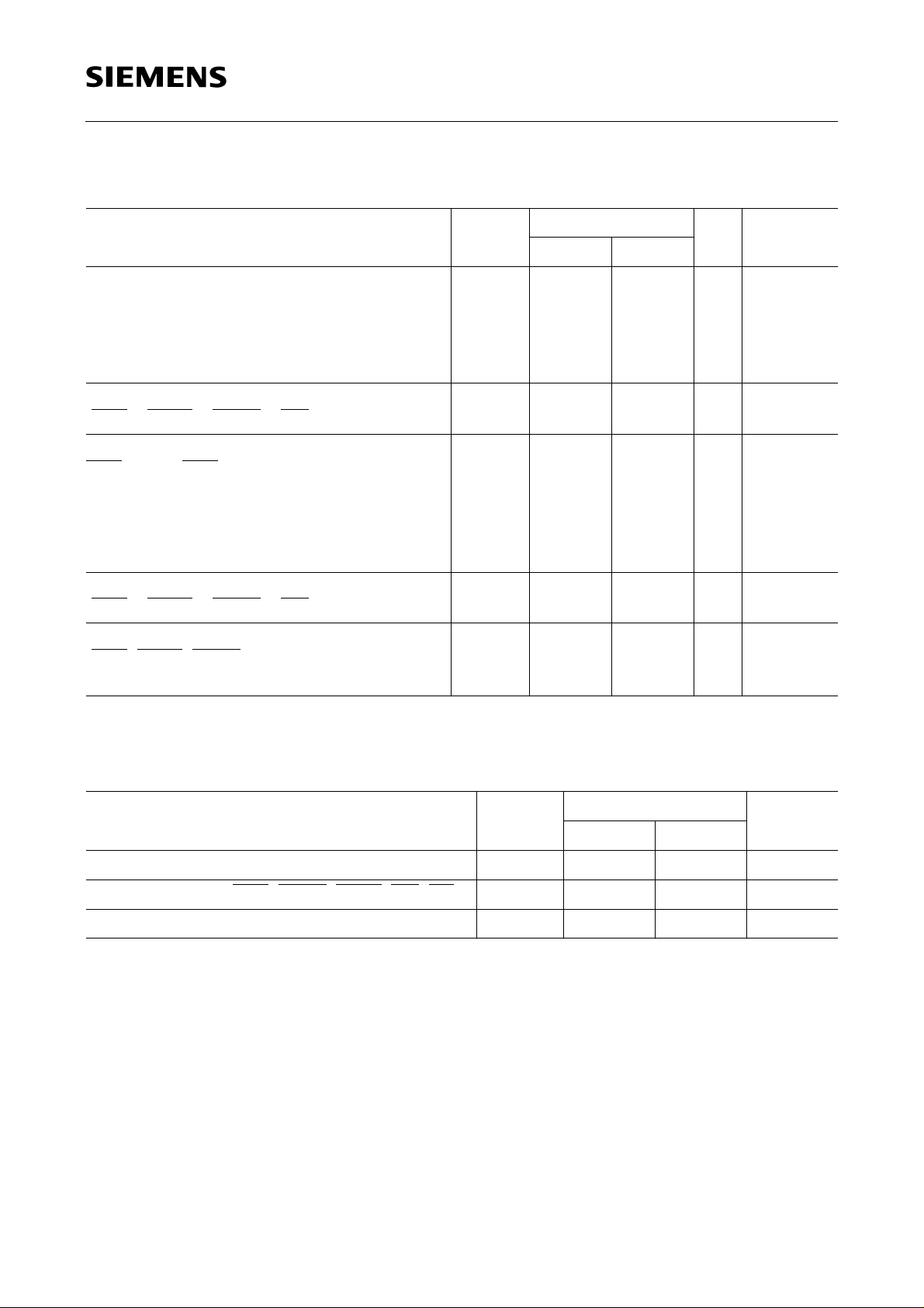
Truth Table
RAS LCAS UCAS WE OE I/O1-I/O8 I/O9-I/O16 Operation
H
L
L
L
L
L
L
L
L
H
H
L
H
L
L
H
L
L
H
H
H
L
L
H
L
L
L
H
H
H
H
H
L
L
L
H
H
H
L
L
L
H
H
H
H
High-Z
High-Z
Dout
High-Z
Dout
Din
Don't care
Din
High-Z
Pin Names
A0-A8 Address Inputs
High-Z
High-Z
High-Z
Dout
Dout
Don't care
Din
Din
High-Z
Standby
Refresh
Lower byte read
Upper byte read
Word read
Lower byte write
Upper byte write
Word write
RAS Row Address Strobe
UCAS, LCAS Column Address Strobe
WE Read/Write Input
OE Output Enable
I/O1 – I/O16 Data Input/Output
V
CC
V
SS
Power Supply (+ 3.3 V)
Ground (0 V)
N.C. No Connection
Semiconductor Group 2
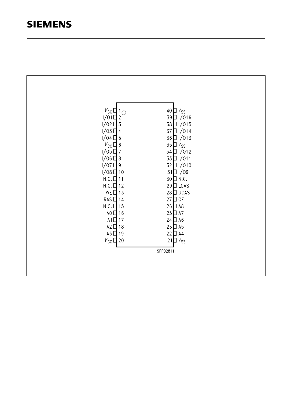
Pin Configuration
(top view)
HYB 314175BJ/BJL-50/-55/-60
3.3V 256K x 16 EDO-DRAM
P-SOJ-40-1
Semiconductor Group 3
HYB 314175BJ/BJL-50/-55/-60
3.3V 256K x 16 EDO-DRAM
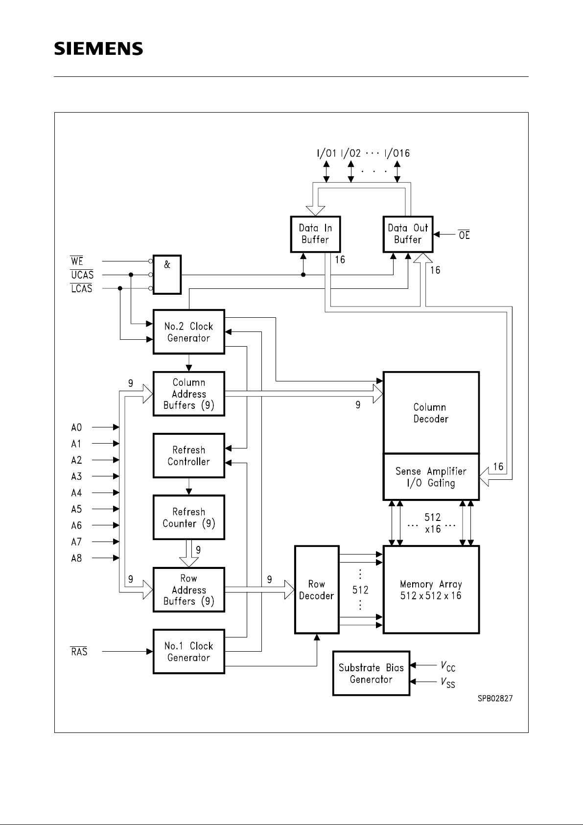
Block Diagram
Semiconductor Group 4
HYB 314175BJ/BJL-50/-55/-60
3.3V 256K x 16 EDO-DRAM
Absolute Maximum Ratings
Operating temperature range ........................................................................................ 0 to + 70 °C
Storage temperature range..................................................................................... – 55 to + 150 °C
Input/output voltage .....................................................................................– 1 to (VCC + 0.5, 4.6) V
Power supply voltage...................................................................................................– 1 to + 4.6 V
Data out current (short circuit) ................................................................................................50 mA
Note:
Stresses above those listed under“Absolute Maximum Ratings” may cause permanent
damage of the device. Exposure to absolute maximum rating conditions for extended periods
may affect device reliability.
DC Characteristics
T
= 0 to 70 °C; VSS = 0 V; VCC = 3.3 V ± 0.3 V, tT = 2 ns
A
Parameter Symbol Limit Values Unit Notes
min. max.
Input high voltage
Input low voltage V
LVTTL Output high voltage (I
LVTTL Output low voltage (I
LVCMOS Output high voltage (I
LVCMOS Output low voltage (I
= – 2.0 mA) V
OUT
= 2 mA) V
OUT
= – 100 µA) V
OUT
= 100 µA) V
OUT
Input leakage current, any input
V
IH
IL
OH
OL
OH
OL
I
I(L)
2.4 VCC + 0.5 V
– 1.0 0.8 V
2.4 – V
– 0.4 V
2.4 – V
– 0.4 V
– 10 10 µA
1
1
1
1
1
1
1
(0 V < VIN < 7 V, all other inputs = 0 V)
Output leakage current
(DO is disabled, 0 V < V
OUT
Average VCC supply current:
< VCC)
-50 version
-55 version
-60 version
I
I
O(L)
CC1
– 10 10 µA
–
125
mA
120
105
1
2, 3, 4
Standby VCC supply current
(RAS = LCAS = UCAS = WE = VIH)
Average
V
supply current during
CC
RAS-only refresh cycles:
-50 version
-55 version
-60 version
Semiconductor Group 5
I
I
CC2
CC3
– 2 mA –
–
125
mA
120
105
2, 4
HYB 314175BJ/BJL-50/-55/-60
3.3V 256K x 16 EDO-DRAM
DC Characteristics (cont’d)
Parameter Symbol Limit Values Unit Test
min. max.
Condition
Average
V
supply current during
CC
hyper page mode (EDO) operation:
-50 version
-55 version
-60 version
Standby VCC supply current
(RAS = LCAS = UCAS = WE = VCC – 0.2 V)
Average VCC supply current during
CAS-before-RAS refresh mode:
-50 version
-55 version
-60 version
Standby VCC current (L-version)
(RAS = LCAS = UCAS = WE = VCC– 0.2 V)
Self Refresh Current (L-version)
RAS, LCAS, UCAS = 0.2V
(
A0–A8=VCC – 0.2 V or 0.2 V)
I
I
I
I
I
CC4
CC5
CC6
CC5
CCS
–
115
mA
2, 3, 4
115
100
–1mA
–
125
mA
1
2, 4
120
105
– 200 µA
– 250 µA
Capacitance
T
= 0 to 70 °C; VCC = 3.3 V ± 0.3 V, f = 1 MHz
A
Parameter Symbol Limit Values Unit
min. max.
Input capacitance (A0 to A8)
Input capacitance (
RAS, UCAS, LCAS, WE, OE) C
Output capacitance (l/O1 to l/O16)
C
C
I1
I2
IO
–5pF
–7pF
–7pF
Semiconductor Group 6
HYB 314175BJ/BJL-50/-55/-60
3.3V 256K x 16 EDO-DRAM
AC Characteristics
T
= 0 to 70 °C; VSS = 0 V; VCC = 3.3 V ± 0.3 V, tT = 2 ns
A
5) 6)
Parameter Symbol Limit Values Unit Note
-50 -55 -60
min max min max min max
Common Parameters
Random read or write cycle time t
RAS precharge time t
RAS pulse width t
CAS pulse width t
Row address setup time
Row address hold time
Column address setup time
Column address hold time
RAS to CAS delaytime t
RAS to column address delay time t
RAS hold time t
CAS hold time t
CAS to RAS precharge time t
Transition time(rise and fall)
Refresh period t
Refresh period (L-version)
t
t
t
t
t
t
RC
RP
RAS
CAS
ASR
RAH
ASC
CAH
RCD
RAD
RSH
CSH
CRP
T
REF
REF
89 – 94 – 104 – ns
35 – 35 – 40 – ns
50 10k 55 10k 60 10k ns
8 10k 8 10k 10 10k ns
0–0–0–ns
8–8–10–ns
0–0–0–ns
8–8–10–ns
12 37 12 43 14 45 ns
10 25 10 30 12 30 ns
13 – 13 – 15 – ns
40 – 45 – 50 – ns
5–5–5–ns
150150150ns
–16–16–16ms
– 128 – 128 – 128 ms
7
Read Cycle
Access time from RAS t
Access time from CAS t
Access time from column address t
OE access time t
Column address to
RAS lead time t
Read command setup time
Read command hold time
Read command hold time ref. to
t
t
t
RAC
CAC
AA
OEA
RAL
RCS
RCH
RRH
–50–55–60ns
–13–13–15ns
–25–25–30ns
–13–13–15ns
25 – 25 – 30 – ns
0–0–0–ns
0–0–0–ns
0–0–0–ns
RAS
CAS to output inlow-Z t
CLZ
0–0–0–ns
Semiconductor Group 7
8, 9
8, 9
8,10
11
11
8
HYB 314175BJ/BJL-50/-55/-60
3.3V 256K x 16 EDO-DRAM
Parameter Symbol Limit Values Unit Note
-50 -55 -60
min max min max min max
Output buffer turn-off delay from
CAS
Output buffer turn-off delay from OE t
Data to OE low delay t
CAS high to data delay t
OE high to data delay t
Write Cycle
Write command hold time t
Write command pulse width
Write command setup time
Write command to RAS lead time t
Write command to
CAS lead time t
Data setup time
Data hold time t
Data to CAS low delay t
t
OFF
OEZ
DZO
CDD
ODD
WCH
t
WP
t
WCS
RWL
CWL
t
DS
DH
DZC
013013015ns
013013015ns
0–0–0–ns
10 – 10 – 13 – ns
10 – 10 – 13 – ns
8–8–10–ns
8–8–10–ns
0–0–0–ns
13 – 13 – 15 – ns
13 – 13 – 15 – ns
0–0–0–ns
8–8–10–ns
0–0–0–ns
12
12
13
14
14
15
16
16
13
Read-modify-Write Cycle
Read-write cycle time t
RAS to WE delay time t
CAS to WE delay time t
Column address to WE delay time t
OE command hold time t
Hyper Page Mode (EDO) Cycle
Hyper page mode cycle time t
CAS precharge time t
Access time from
CAS precharge t
Output data hold time t
RAS pulse width in hyper page
mode
RAS hold time from CAS precharge t
RWC
RWD
CWD
AWD
OEH
HPC
CP
CPA
COH
t
RAS
RHCP
118 – 122 – 138 – ns
64 – 69 – 77 – ns
27 – 27 – 32 – ns
39 – 39 – 47 – ns
10 – 10 – 13 – ns
20 – 20 – 25 – ns
8–8–10–ns
–27–27–32ns
5–5–5–ns
50
200k
55
200k
60
200k
ns
27 – 27 – 32 – ns
15
15
15
7
Semiconductor Group 8
 Loading...