

SGS Thomson Microelectronics LM346D, LM346, LM346N, LM246, LM146 Datasheet
November1997
PROGR AMMABL E
QUAD BIPOLAR OPERAT ION AL AMPL IFI ERS
.PROGRAMMABLE ELECTRICAL CHARAC-
TERISTICS
.BATTERYPOWEREDOPERATION
.LOW SUPPLY CURRENT (250µA/amplifier)
.GAIN-BANDWIDTH PRODUCT: 1MHz
.LARGEDC VOLTAGEGAIN : 120dB
.LOW NOISEVOLTAGE: 28nV/VHz
.WIDE POWERSUPPLYRANGE:
±1.5Vto
±22V
.CLASSE AB OUTPUT STAGE. NO CROSS-
OVERDISTORTION
.OVERLOADPROTECTION FOR INPUTS AND
OUTPUTS
DESC RIP TI ON
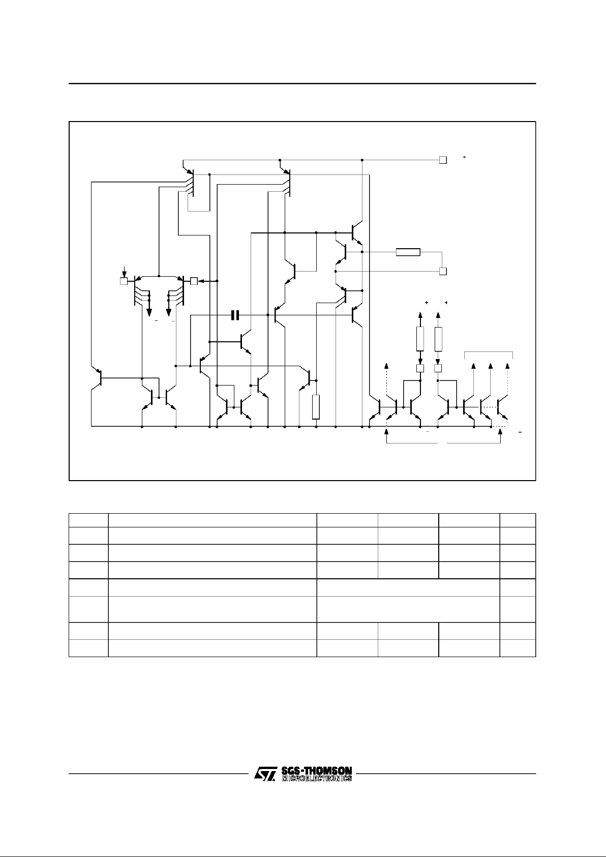
The LM346consistsof fourindependent,highgain,
internallycompensated,low power programmable
amplifiers. Two external resistors (R
set
) allow the
user to program the gain-bandwith product, slew
rate,supply current,inputbias current,input offset
currentand input noise. For example the user can
trade-off supply current for bandwidth or optimize
noisefigurefora givensource resistance.In a similar wayother amplifiercharacteristicscanbe
tailoredto theapplication.
Exceptfor thetwo programming pins at the end of
the packagethe LM346pin out is the sameas the
LM324and LM348.
PROGRAMMINGEQUATIONS:
Totalsupplycurrent= 1mA(I
set
=10µA)
Gain-bandwidthproduct = 1MHz (I
set
=10µA)
Slewrate = 0.5V/µs(I
set
=10µA)
Inputbias current ≈30 nA (I
set
=10µA)
I
set
=currentinto pin8 and pin 9
(see schematicdiagram)
I
set
=
V
CC
+
− V
CC
−
− 0.6V
R
set
4
5
6
7
9
10
11
12
13
15
1
2
3
8
16
14
Output1
Invertinginput 1
Non-invertinginput1
Non-invertinginput 2
Invertinginput 2
Output2
Set
Output4
Invertinginput 4
Non-invertinginput 4
V
CC
Non-invertinginput 3
Invertinginput 3
Output3
Set
V
CC
+
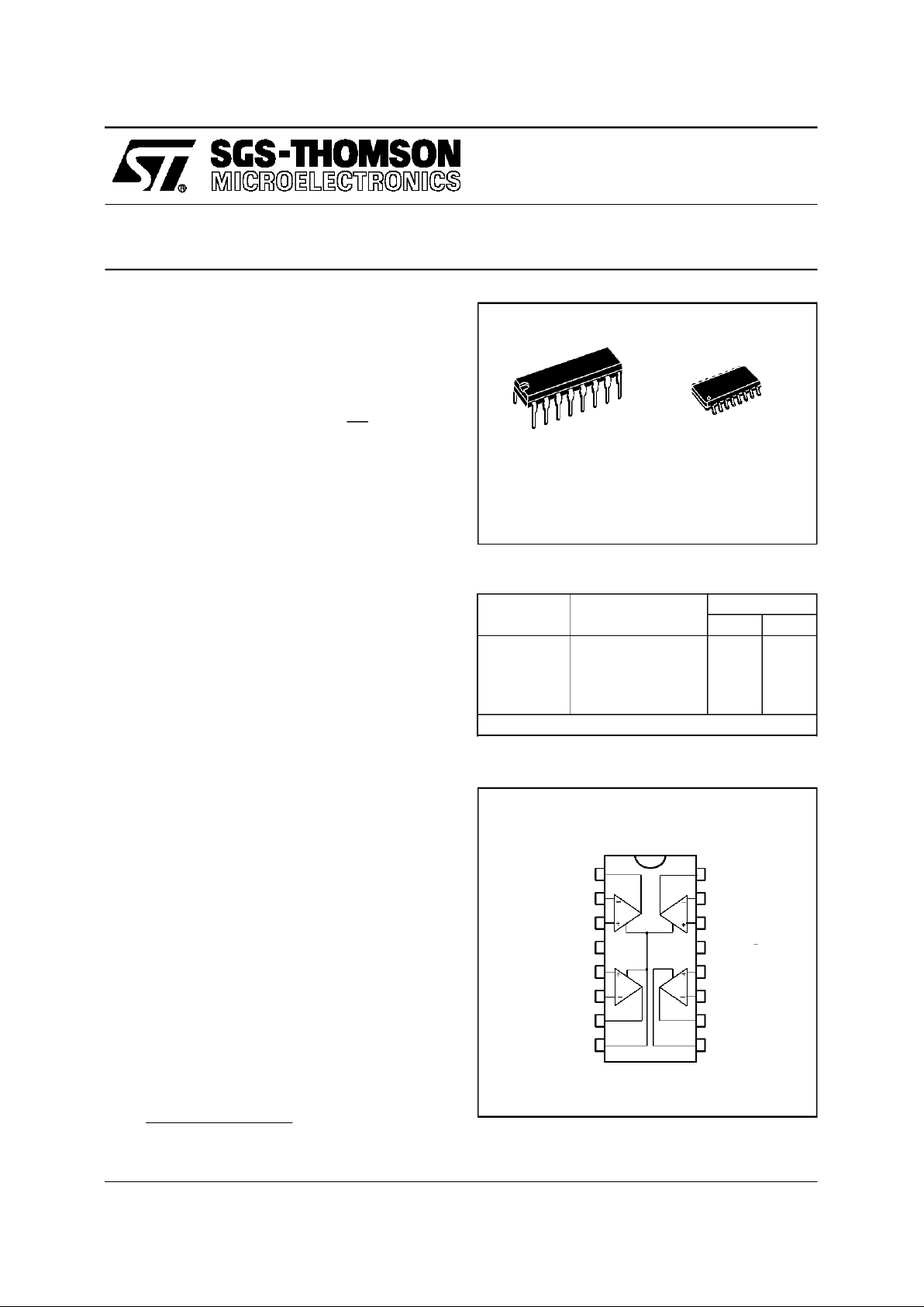
PIN C O NNEC TIO NS (top view)
ORDER CODES
Part
Number
Temperature
Range
Package
ND
LM146 –55
o
C, +125oC ••
LM246 –40
o
C, +105oC ••
LM346 0
o
C, +70oC ••
Example : LM246N
N
DIP16
(PlasticPackage)
D
SO16
(PlasticMicropackage)
LM146
LM246 - LM346
1/9
Notes : 1. For supply volt ages less than ±15V, the absolute maxi mum i nput voltage is equal t o the s upply vol tage.
2. Any of the ampl ifier output s can be shorted t o g r ound indefi nitly ; howev e r m or e t han one should n ot be
simul t aneous l y shorted as the maximum junction temperat ur e wi ll be exceeded.
ABSOLUTE MAXIMUM RATINGS
Symbol Parameter LM146 LM246 LM346 Unit
V
CC
Supply Voltage ±22 ±22 ±22
V
V
i
Input Voltage - (note 1) ±15 ±15 ±15 V
V
id
Differential Input Voltage ±30 ±30 ±30 V
Output Short-circuit Duration - (note 2) Infinite
P
tot
Power Dissipation
N/D Suffix 500
mW
T
oper
Operating Free-air Temperature Range –55 to +125 –40 to +105 0 to +70
o
C
T
stg
Storage Temperature Range –65 to +150 –65 to +150 –65 to +150
o
C
V
CC
V
CC
V
CC
or
Q18 Q19
Toother op amps
V
CCVCC
Output
R
set
R
set
I
set
I
set
SET
SET
R1
30Ω
Q12
Q10
Q11
Q9
Q16
Q15
Q14
Q13
8pF
C
C
Non-
inverting
input
Q20
Q6
Q8
Q5
R2
1kΩ
Q7Q21
Q4
Q3
Q17
V
CC
V
CC
Q1 Q2
Inverting
input
SCHE MATIC DIAGRAM ( 1/4 LM146)
LM146 - LM246 - LM346
2/9
ELECTRICAL CHARACTERISTICS
V
CC
= ±15V, I
set
=10µA, T
amb
= +25oC (unlessotherwise specified)
Symbol Parameter
LM146 LM246 - LM346
Unit
Min. Typ. Max. Min. Typ. Max.
V
io
Input Offset Voltage (RS≤ 10kΩ)
T
amb
=25oC
T
min
. ≤ T
amb
≤ T
max.
0.5 3
5
0.5 5
6
mV
I
io
Input Offset Current
T
amb
=25oC
T
min
. ≤ T
amb
≤ T
max.
220
25
2 100
100
nA
I
ib
Input Bias Current
T
amb
=25oC
T
min
. ≤ T
amb
≤ T
max.
30 100
100
30 250
250
nA
A
vd
Large Signal Voltage Gain
(V
o
= ±10V, RL= 10kΩ)
T
amb
=25oC
T
min
. ≤ T
amb
≤ T
max.
100501000 50251000
V/mV
SVR Supply Voltage Rejection Ratio (R
S
≤ 10kΩ)
T
amb
=25oC
T
min
. ≤ T
amb
≤ T
max.
8080110 8080110
dB
I
CC
Supply Current, all Amp, no Load
T
amb
=25oC
T
min
. ≤ T
amb
≤ T
max.
12
2
12
2
mA
V
icm
Input Common Mode Voltage Range
T
amb
=25oC
T
min
. ≤ T
amb
≤ T
max.
±13.5
±13.5
±13.5
±13.5
V
CMR Common Mode Rejection Ratio (R
S
≤ 10kΩ)
T
amb
=25oC
T
min
. ≤ T
amb
≤ T
max.
8070110 8070110
dB
I
OS
Output Short-circuit Current
T
amb
=25oC
T
min
. ≤ T
amb
≤ T
max.
10
4
20 30
35
10
4
20 30
35
mA
± V
opp
Output Voltage Swing (RL= 10kΩ)
T
amb
=25oC
T
min
. ≤ T
amb
≤ T
max.
12
12
14 12
12
14
V
SR Slew Rate (V
I
= ±10V, RL= 10kΩ,CL= 100pF,
unity Gain) 0.3 0.5 0.3 0.5
V/µs
R
I
Input Resistance 1 1 MΩ
C
I
Input Capacitance 2 2 pF
V
o1/Vo2
Channel Separation (RL= 10kΩ,Vo= 12Vpp) 120 120 dB
GBP Gain Bandwidth Product
(V
I
= 10 mV, RL= 10kΩ,CL= 100pF
f = 100kHz) 0.8 1 0.5 1
MHz
THD Total Harmonic Distortion
(f = 1kHz, A
v
= 20dB, RL= 10kΩ
C
L
= 100pF, vo=2Vpp) 0.015 0.015
%
e
n
Equivalent Input Noise Voltage
(f = 1kHz, R
s
= 100Ω)
28 28
nV
√Hz
LM146 - LM246 - LM346
3/9
 Loading...