

LM139,A
LOWPOWER QUAD VOLTAGE COMPARATORS
.WIDESINGLESUPPLYVOLTAGERANGEOR
DUALSUPPLIESFOR ALLDEVICES: +2V TO
+36V OR±1VTO ±18V
.VERY LOW SUPPLY CURRENT (1.1mA)
INDEPENDENT OF SUPPLY VOLTAGE
(1.4mW/comparatorat+5V)
.LOW INPUT BIAS CURRENT: 25nATYP
.LOW INPUT OFFSETCURRENT : ±5nATYP
.LOW INPUT OFFSETVOLTAGE: ±1mV TYP
.INPUT COMMON-MODE VOLTAGE RANGE
INCLUDES GROUND
.LOW OUTPUT SATURATION VOLTAGE :
250mV TYP.(I
=4mA)
O
.DIFFERENTIAL INPUT VOLTAGE RANGE
EQUALTOTHESUPPLYVOLTAGE
.TTL, DTL, ECL, MOS, CMOS COMPATIBLE
OUTPUTS
DESC RIP TI ON
Thesedevicesconsistof fourindependentprecision
voltagecomparatorswith an offset voltagespecifications as low as 2mVmax for LM339A,LM239A
and LM139A.All thesecomparatorsweredesigned
specifically to operatefrom a single power supply
over a wide range of voltages. Operationfrom split
powersuppliesis alsopossible.
Thesecomparatorsalsohavea uniquecharacteristic in that the input common-modevoltagerange
includesgroundeventhoughoperatedfromasingle
powersupplyvoltage.
LM239,A-LM339,A
N
DIP14
(PlasticPackage)
TSSOP14
(Thin Shrink Small Outline Package)
ORDER CODES
Part
Number
LM139,A -55, +125
LM239,A -40, +105
LM339,A 0, +70
Example : LM139AN
Temperature
Range
D
SO14
(PlasticMicropackage)
P
Package
o
C •••
o
C •••
o
C •••
NDP
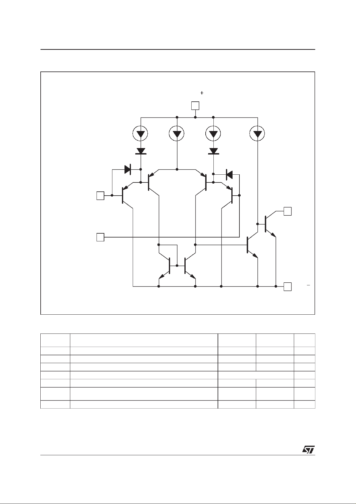
PI N CONNECTIONS (top view)
Invertinginput1
Non-invertinginput1
Invertinginput2
Non-invertinginput2
June 1998
1
Output2
2
Output1
+
V
3
CC
4
5
6
7 8
Output3
14
13
Output4
-
12
V
CC
11
Non-invertinginput4
10
Invertinginput4
9
Non-invertinginput3
Invertinginput3
1/10
LM139,A - LM239,A - LM339,A
SCHE MATIC DIAGRAM (1/4 LM139)
V
CC
Non-inverting
Input
Inverting
Input
3.5µA100
µ
A 3.5µA100
µ
A
V
O
V
CC
ABSOLUTE MAXIMUM RATINGS
Symbol Parameter
V
V
V
P
T
oper
T
Notes : 1. Short-cir cuit fr om t he output to V
2/10
Supply Voltage ±18 to 36 ±18 to 36 V
CC
Differential Input Voltage ±36 ±36 V
id
Input Voltage -0.3 to +36 -0.3 to +36 V
I
Output Short-circuit to Ground - (note 1) Infinite
Power Dissipation 570 570 mW
tot
Operating Free-air Temperature Range
Storage TemperatureRange -65, +150 -65, +150
stg
output current is approximately 20mA, i ndependent of the magnitude of V
LM139,A
LM239,A
LM239,A
+
can cause excess ive heating and eventual dest ruction. Th e maximum
CC
-55, +125
-40, +105
+
.
CC
LM339,A Unit
0, +70
o
C
o
C
ELECTRICAL CHARACTERISTICS
V
CC
+
= +5V, V
-
= GND, T
CC
=25oC (unless otherwise specified)
amb
Symbol Parameter
V
Input Offset Voltage – (note 2)
io
Input Offset Current
I
io
Input Bias Current (I
I
ib
Large Signal Voltage Gain
A
vd
I
Supply Current (all comparators)
CC
V
V
Notes : 2. At output switchpoint, VO≈ 1.4V, RS=0withV
Input Common Mode Voltage Range - (note 4)
icm
Differential Input Voltage - (note 6) V
V
id
Low Level Output Voltage
OL
High Level Output Current ( Vid= 1V)
I
OH
Output Sink Current
I
sink
t
Response Time – (note 5)
re
t
Large Signal Response Time
rel
(0V t o V
3. The direct ion of the input curr ent i s out of the IC due t o t he PN P i nput stage. This current is essentially constant, i ndependent of the st ate of the output, so no loading charge exi sts on t he reference of input lines.
4. The input common- mode voltage of ei t her input si gn al vol tage s h ould no t be allow ed to go ne gati v e by more
than 0.3V. T he upper end of the common-mode voltage r ange is V
to +30V withou t damage .
5. The response time specifi ed is for a 100mV input step with 5mV overdrive. For larger overdrive signals 300ns
can be obtained.
6. Positive exc ursions o f input voltage may exceed the p ower supp ly lev el. As long as the other voltage r emai ns
withi n the common-mode r ange, the comp a r ator w ill pr ovide a proper ou t put state. T he lo w in put voltag e st ate
must n ot be less t han –0.3V (or 0.3 V bellow the negati ve power su pply, i f used).
= +25oC
T
amb
≤ T
T
min.
T
amb
T
min.
T
amb
T
min.
(V
CC
V
CC
V
CC
(V
CC
T
amb
. ≤ T
T
min
= -1V, I
(V
id
T
amb
T
min.
(V
CC=VO
T
amb
. ≤ T
T
min
= -1V, VO= 1.5V) 6 16 6 16
(V
id
= 5.1kΩ connected to V
(R
L
= 5.1kΩ connected to V
(R
L
V
(ref)
CC
≤ T
amb
max.
= +25oC
≤ T
≤ T
amb
max.
+
–
or I
) - (note 3)
I
= +25oC
≤ T
amb
≤ T
I
max.
= 15V, RL=15kΩ,VO= 1 to 11V) 50 200 50 200
= +5V, no load
= +30V, no load
= 30V)
= +25oC
≤ T
amb
max.
= 4mA)
sink
= +25oC
≤ T
≤ T
amb
max.
= 30V)
= +25oC
≤ T
amb
max.
+
) 1.3 1.3
CC
+
,eI= TTL,
= +1.4V) 300 300
+
–1.5V).
CC
LM139,A - LM239,A - LM339,A
LM139A - LM239A
LM339A
Min. Typ. Max. Min. Typ. Max.
12
4
325
100
25 100
300
1.1
1.3
0
0
2
2.5
+
V
-1.5
CC
+
-200
V
CC
+
CC
250 400
700
0.1
1
+
from 5Vto 30V, and over the full input common-mode range
CC
+
–1.5V, but ei ther or both inputs can go
CC
LM139 - LM239
LM339
15
550
150
25 250
400
1.1
1.3
2.5
V
CC
V
CC
V
250 400
700
0.1
9
2
+
-1.5
+
-2
+
CC
1
Unit
mV
nA
nA
V/mV
mA
V
V
mV
nA
µA
mA
µs
ns
3/10
 Loading...