


查询LNK305供应商
RT8800/B
General Purpose 2/3-Phase PWM Controller
for High-density Power Supply
General Description
The RT8800/B are general purpose multi-phase
synchronous buck controllers dedicating for high density
power supply regulation. The parts implement 2, and 3
buck switching stages operating in interleaved phase set
automatically. The output voltage is regulated and
controlled following the input voltage of FB pin. With such
a single analog control, the RT8800/B provide a simple,
flexible, wide-range and extreme cost-effective highdensity voltage regulation solutions for various high-density
power supply application. The RT8800/B multi-phase
architecture provide high output current while maintaining
low power dissipation on power devices and low stress
on input and output capacitors. The high equivalent
operating frequency also reduces the component
dimension a nd the output voltage ripple in load tra nsient.
RT8800/B implement both voltage and current loops to
achieve good regulation, response and power stage
thermal balance. The RT8800/B apply the time sharing
DCR current sensing technology newly a s well; with such
a topology, the RT8800/B extract the DCR of output
inductor as sense component to deliver a more precise
load line regulation and better thermal bala nce ca pability .
Moreover, the parts monitor the output voltage f or overcurrent and over-voltage protection; Soft-start and
programma ble under-voltage lockout are also provided to
a ssure the safety of power system.
Applications
Desktop CPU core power
Low Output Voltage, High power density DC-DC
Converters
V oltage Regulator Modules
Marking Information
For marking information, contact our sales re presentative
directly or through a RichTek distributor located in your
area, otherwise visit our website for detail.
Features
5V Power Supply Voltage
2/3-Phase Power Conversion with Automatic Phase
Selection (RT8800 : 2/3-Phase, RT8800B : 2-Pha se)
Output Voltage Controlled by External Reference
Voltage
Precise Core Voltage Regulation
Power Stage Thermal Balance by DCR Current
Sensing
Extreme Low-Cost, Lossless Time Sharing Current
Sensing
Internal Soft-start
Hiccup Mode Over-Current Protection
Over-Voltage Protection
Adjustable Operating Frequency and Typical at
300kHz Per Phase
Power Good indication
Small 16-Lead VQFN Package (For RT8800 only)
RoHS Compliant and 100% Lead (Pb)-Free
Ordering Information
RT8800/B
Package Type
QV : VQFN-16L 3x3 (Pb Free Only)
S : SOP-16
Operating Temperature Range
C : Commercial Standard
P : Pb Free with Commercial Standard
2-Phase
2/3-Phase
Note :
VQFN-16L 3x3 is in V-Type
RichTek Pb-free products are :
`RoHS compliant and compatible with the current require ments of IPC/JEDEC J-STD-020.
`Suitable for use in SnPb or Pb-free soldering processes.
`100% matte tin (Sn) plating.
All brand name or trademark belong to their owner respectively
DS8800/B-04 November 2005 www.richtek.com
1

RT8800/B
Pin Configurations
(TOP VIEW)
PWM3
GND
PI
PWM2
RT
PWM1
13141516
ISP1
12
ISP2
11
ISP3
10
PGOOD
9
8765
ICOM MON
DACFB
DACQ
FB
DVD
VDD
1
2
3
4
COMP
VQFN-16L 3x3
RT8800
Functional Pin Description
DACFB
Negative input of internal buffer amplifier for reference
voltage regulation. The pin voltage is locked at internal
V
= 0.8V by properly close the buffer a mplifier feedback
REF
loop.
DACQ
The pin is defined a s the output of internal buffer a mplifier
for reference voltage regulation.
FB
The pin is defined as the inverting input of internal error
amplif ier.
DVD
The pin is defined as a programmable power UVLO
detection input. T ri p threshold = 0.8V at V
DVD
rising.
VDD
DACFB
DACQ
FB
DVD
COMP
RT ICOMMON
2
3
4
5
6
7
PI
16
PWM2
15
PWM1
14
N/C
13
ISP1
12
ISP2
11
PGOOD
10
GND
98
SOP-16
RT8800B
ICOMMON
Common negative input of current sense a mplifiers for all
three channels.
PGOOD
Output power-good indication. The signal is implemented
a s a n output signal with open-drain type.
ISP1 , ISP2 , ISP3
Current sense positive inputs for individual converter
channel current sense.
PWM1 , PWM2 , PWM3
PWM outputs for ea ch pha se switching drive.
VDD
Chip power supply. Connect this pin to a 5V supply.
COMP
The pin is defined a s the output of the error a mplifier a nd
the input of all PWM comparators.
PI
The pin is defined a s the positive input of the error amplif ier.
RT
Switching frequency setting. Connect this pin to GND with
a resistor to set the frequency.
All brand name or trademark belong to their owner respectively
2
GND
Chip power ground.
Exposed Pad (RT8800)
Exposed pad should be soldered to PCB board and
connected to GND.
DS8800/B-04 November 2005www.richtek.com
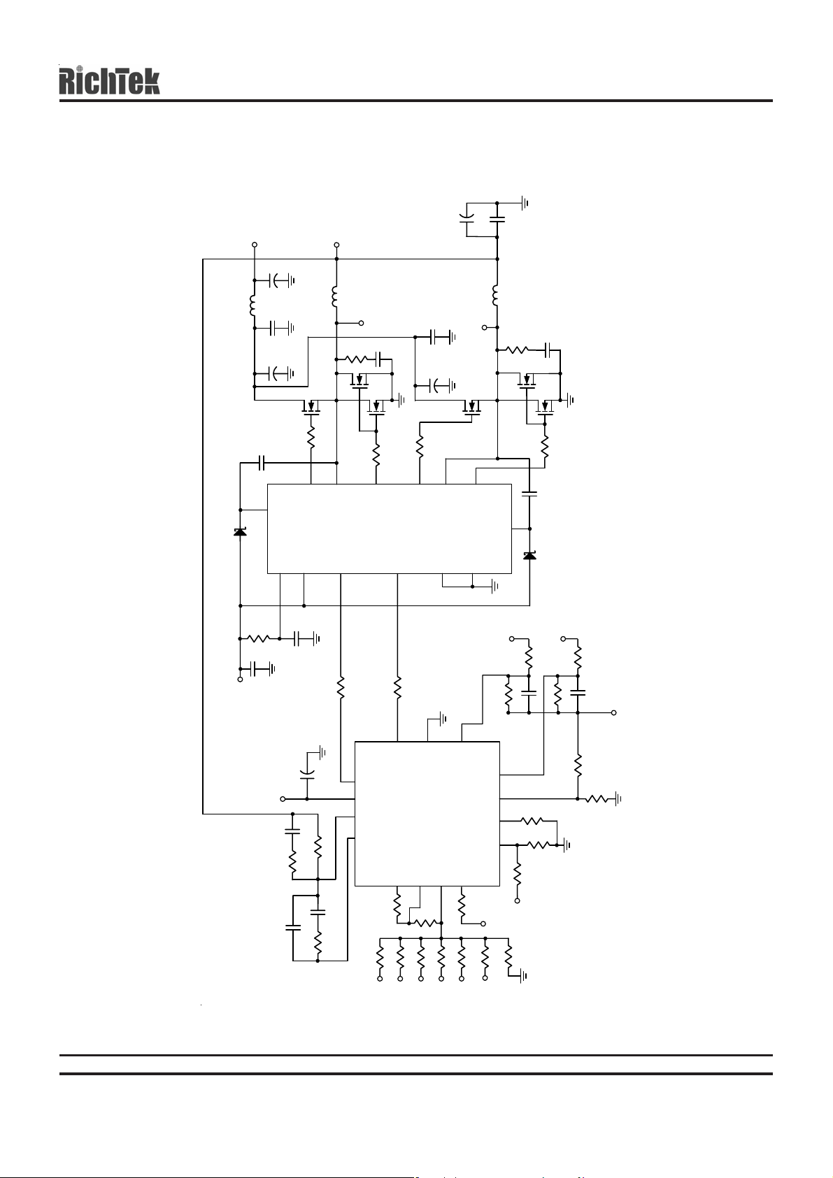
Typical Application Circuit
(Note : The inductor’ s DCR value must be large than 0.3mΩ
: X7R/R-type capacitor is required for all time constant setting capacitor of DCR sensing.)
CORE
Q1
R21
5
L2
0
12
UGATE1
PVCC
V
0.5uH
2.2
R25
Q2
PHB83N03LT
13
PHASE1
RT9602
PWM1
1
PHASE1
0
R22
4
C14
3.3nF
Q3
PHB95N03LT
LGATE1
PWM2
2
R23
C18 to C29
1000uF x 12
C16
1uF
C15
2200uF
Q4
0
7
8
9
UGATE2
PHASE2
L3
0.5uH
PHASE2
PHB83N03LT
LGATE2
C30 to C33
10uF x 4
R26
10
2.2
Q5
R24
C17
Q6
0
1uF
C10
3.3nF
PHB95N03LT
BOOT2
D2
SS12/SM
3
GND
PGND
6
D1
SS12/SM
L1
C13
1uH
12V
1000uF
C12
C9
1uF
11
1uF
C11
2200uF
BOOT1
VDD
14
RT8800/B
12V
C7
C8
R20
1uF
1uF
10
Optional for
5V
C1
R & C
33pF
C4
0
R16
15
1
4
6
C3
3k
R3
R2
C2
10nF
R1
15k
PWM1
VDD
FB
COMP
110k
R4
R17
DROOP
R
VID5
0
16
PWM2
PI
7
56k
R5
VID0
DACQ
3
27k
R6
VID1
10
GND
RT8800B
2
R11
1.8k
13k
R7
DACFB
VID2
ICOM M ON
Figure A. 2-phase with resistive DAC
12
ISP2
PGOOD
11
6.8k
R8
VID3
ISP1
DVD
10k
R12
3.3k
R9
RT
3.3V
VID4
PHASE2
R18
Optional
13
9
8
5
5.1k
R10
R
12V
C5
R13
1uF
R15
27k
16k
R14
3k
PHASE1
R19
Optional
R
430
R
Optional
C6
ICOMMON1
1uF
R
CORE
V
ICOMMON2
All brand name or trademark belong to their owner respectively
DS8800/B-04 November 2005 www.richtek.com
3
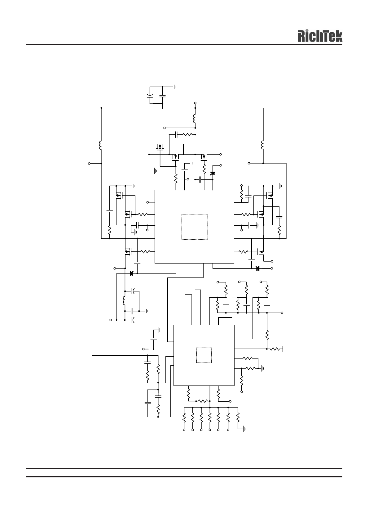
RT8800/B
L1
0.5uH
CORE
R27
L2
2.2
V
0.5uH
L3
Q9
IN
V
0.5uH
C24 to C35
1000uF x 12
10uF x 4
C36 to C39
PHASE3
C23
3.3nF
Q7
Q8
PHASE2
Q3
3.3uF
C16
Q2
2.2
R19
R20
C15
1uF
0
12V
NC
3
20
21
1uF
C21
0
R25
14
15
LGATE3
LGATE2
12V
11
PVCC3
0
R26
10
PHASE3
UGATE3
PVCC2
GND
RT9605
PHASE2
D3
9
C22
BOOT3
1uF
12V
PHASE1
SB
5V
10
1uF
VDD
R23
C19
8
0
R22
LGATE1
PVCC1
C18
1uF
12V
PHASE1
Q6
3.3nF
C20
2.2
R24
1917
R21
UGATE1
1242223
PHASE2
R17
Optional
12
8
7
4
27k
R13
3.3V
5.1k
R10
C17
R
12V
0
1uF
C6
R15
1uF
R14
16k
3k
D2
PHASE1
R17
Optional
R
430
Q4 Q5
IN
V
12V
C7
1uF
ICOMMON1
R
Optional
ICOMMON2
R
CORE
V
12V
0
D1
C9
1uF
C8
1000uF
C14
C10 to C13
5V
C2
Optional
C1
33pF
R18
1uF
1500uF x 4
C4
4.7uF
R2
Q1
IN
V
1uH
UGATE2
BOOT2
PWM3
PWM2
PWM1
BOOT1
5
RT8800
DACQ
2
14
PWM2
R11
27k
4
10
GND
1.8k
13k
R7
2
PHASE3
R16
Optional
11
ISP3
ISP2
ICOMMON
DACFB
PGOOD
1
9
6.8k
R8
R
1uF
C5
ISP1
DVD
R12
3.3k
R9
RT
10k
7
16
15
PWM3
PWM1
13
16
VDD
3
FB
5
3k
COMP
R3
PI
6
C3
10nF
DROOP
R
R1
15k
56k
110k
R4R5R6
VID0
VID2
VID3
VID1
VID5
VID4
Figure B. 3-phase with re sistive DAC
All brand name or trademark belong to their owner respectively
DS8800/B-04 November 2005www.richtek.com
4
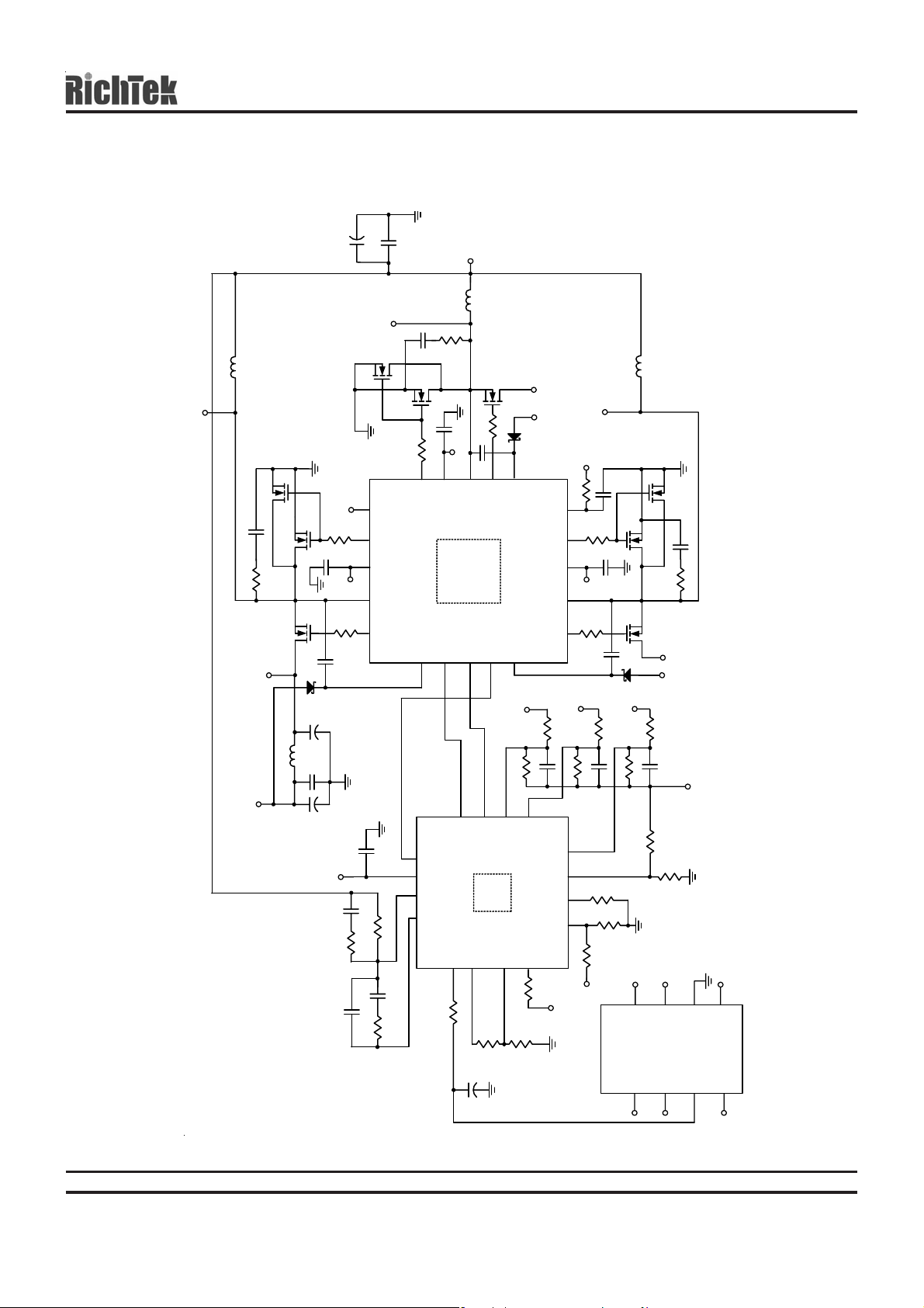
RT8800/B
CORE
C25 to C36
1000uF x 12
L1
0.5uH
PHASE3
Q7
C24
C37 to C40
3.3nF
10uF x 4
Q8
V
L2
0.5uH
2.2
R22
Q9
IN
V
L3
0.5uH
PHASE2
C16
3.3uF
2.2
R14
12V
9
C23
BOOT3
1uF
12V
PHASE1
SB
5V
10
1uF
VDD
R19
C20
8
0
R18
LGATE1
PVCC1
PHASE1
1uF
C19
12V
Q6
C21
3.3nF
Q5
2.2
R17
1uF
0
15
PVCC3
12V
11
PHASE3
GND
R21
10
UGATE3
C22
0
R20
14
Q3
Q2
R15
C17
1uF
12V
NC
3
0
20
21
LGATE3
LGATE2
PVCC2
RT9605
PHASE2
1917
R13
D1
C10
1uF
1000uF
C15
C11 to C14
5V
C3
Optional
C1
33pF
0
1uF
1500uF x 4
C5
R2
4.7uF
Q1
IN
V
1uH
C9
UGATE2
BOOT2
PWM3
PWM2
PWM1
BOOT1
5
RT8800
DACQ
2
4
14
PWM2
R4
2
R10
10
ISP3
ICOMMON
GND
DACFB
1
5.1k
PHASE3
Optional
11
ISP2
PGOOD
9
5.1k
R5
R
1uF
C6
ISP1
DVD
R6
7
16
15
PWM3
PWM1
13
16
VDD
3
FB
5
3k
COMP
R3
PI
6
C2
10nF
R1
15k
R
DROOP
RT
10k
UGATE1
12
8
7
4
3.3V
1242223
PHASE2
R11
Optional
27k
R7
R16
12V
C18
R
C7
0
1uF
R9
1uF
R8
16k
R12
3k
D2
PHASE1
R
Optional
430
8
VID3
Q4
IN
V
12V
C8
1uF
CORE
V
ICOMMON1
R
Optional
ICOMMON2
R
5
6
7
GND
VID4
VID0
C4
10nF
RT9401A/B
VID1
VID2
1
2
3
VDA
VDD
4
5V
Figure C. 3-phase with RT9401A/B DAC generator
All brand name or trademark belong to their owner respectively
DS8800/B-04 November 2005 www.richtek.com
5
RT8800/B
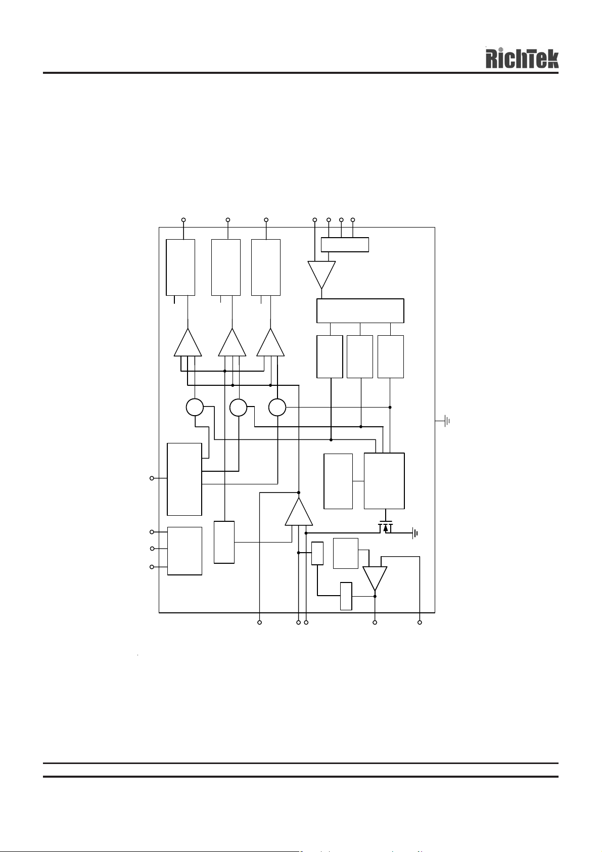
Oscillator
&
Ramp Generator
+
+
+
+
+
+
Sample
& Hold
PWM1
PWM2
PWM3
OCP
SUM/N
& OCP
Detection
PGOOD
DVD
GND
Soft Start
+
+
-
ICOMMON
ISP1
ISP2
ISP3
PWM Logic
& Driver
PWMCP
+
-
PWM Logic
& Driver
PWMCP
+
-
PWM Logic
& Driver
PWMCP
+
-
+
+
+
Mux
Mux
Sample
& Hold
Sample
& Hold
VDD
FB
EA
GM
COMP
-
+
-
0.8V
V
REF
PI
Buffer
Amplifier
INH
INH
INH
Power On
Reset
RT
MAJ
500mV
OVP
DACFB
DACQ
Function Block Diagram
All brand name or trademark belong to their owner respectively
6
DS8800/B-04 November 2005www.richtek.com

RT8800/B
VID5 VID4 VID3 VID2 VID1 VID0 Nominal Output Voltage (V)
1 1 1 1 1 1 1.0800
1 1 1 1 1 0 1.1000
0 1 1 1 1 0 1.1125
1 1 1 1 0 1 1.1250
0 1 1 1 0 1 1.1375
1 1 1 1 0 0 1.1500
0 1 1 1 0 0 1.1625
1 1 1 0 1 1 1.1750
0 1 1 0 1 1 1.1875
1 1 1 0 1 0 1.2000
0 1 1 0 1 0 1.2125
1 1 1 0 0 1 1.2250
0 1 1 0 0 1 1.2375
1 1 1 0 0 0 1.2500
0 1 1 0 0 0 1.2625
1 1 0 1 1 1 1.2750
0 1 0 1 1 1 1.2875
1 1 0 1 1 0 1.3000
0 1 0 1 1 0 1.3125
1 1 0 1 0 1 1.3250
0 1 0 1 0 1 1.3375
1 1 0 1 0 0 1.3500
0 1 0 1 0 0 1.3625
1 1 0 0 1 1 1.3750
0 1 0 0 1 1 1.3875
1 1 0 0 1 0 1.4000
0 1 0 0 1 0 1.4125
1 1 0 0 0 1 1.4250
0 1 0 0 0 1 1.4375
1 1 0 0 0 0 1.4500
0 1 0 0 0 0 1.4625
1 0 1 1 1 1 1.4750
0 0 1 1 1 1 1.4875
1 0 1 1 1 0 1.5000
0 0 1 1 1 0 1.5125
1 0 1 1 0 1 1.5250
0 0 1 1 0 1 1.5375
1 0 1 1 0 0 1.5500
Table. Output Voltage Program
To be continued
All brand name or trademark belong to their owner respectively
DS8800/B-04 November 2005 www.richtek.com
7

RT8800/B
VID5 VID4 VID3 VID2 VID1 VID0 Nominal Output Voltage (V)
0 0 1 1 0 0 1.5625
1 0 1 0 1 1 1.5750
0 0 1 0 1 1 1.5875
1 0 1 0 1 0 1.6000
1 0 1 0 0 1 1.6250
1 0 1 0 0 0 1.6500
1 0 0 1 1 1 1.6750
1 0 0 1 1 0 1.7000
1 0 0 1 0 1 1.7250
1 0 0 1 0 0 1.7500
1 0 0 0 1 1 1.7750
1 0 0 0 1 0 1.8000
1 0 0 0 0 1 1.8250
1 0 0 0 0 0 1.8500
Note: 1 : Open
or GND
0 : V
SS
Table. Output Voltage Program
All brand name or trademark belong to their owner respectively
DS8800/B-04 November 2005www.richtek.com
8
Absolute Maximum Ratings (Note 1)
RT8800/B
Supply Voltage, V
Input, Output or I/O Voltage---------------------------------------------------------------------------------- GND − 0.3V to V
Power Dissipation, P
------------------------------------------------------------------------------------------- 7V
DD
@ T
D
= 25°C
A
VQF N-16L 3X3 -------------------------------------------------------------------------------------------------- 1.47W
SOP-16 ----------------------------------------------------------------------------------------------------------- 1W
Package Thermal Resistance (Note 4)
VQF N-16L 3X3, θJA--------------------------------------------------------------------------------------------- 68°C/W
SOP-16, θJA----------------------------------------------------------------------------------------------------- 100°C/W
Junction T emperature------------------------------------------------------------------------------------------ 150°C
Lead T e mperature (Soldering, 10 sec.)-------------------------------------------------------------------- 260 °C
Storage T emperature Range --------------------------------------------------------------------------------- −65°C to 150°C
ESD Susceptibility (Note 2)
HBM (Human Body Mode) ----------------------------------------------------------------------------------- 2kV
MM (Ma chine Mode)------------------------------------------------------------------------------------------- 200V
Recommended Operating Conditions (Note 3)
Supply V oltage, V
Ambient T emperature Range--------------------------------------------------------------------------------- 0°C to 70°C
Junction T emperature Range--------------------------------------------------------------------------------- 0°C to 125°C
------------------------------------------------------------------------------------------- 5V ± 10%
DD
DD
+ 0.3V
Electrical Characteristics
(V
= 5V , TA = 25°C, unless otherwise specified)
DD
Parameter Symbol Test Conditions Min Typ Max Units
V
Supply Current
DD
Nominal Supply Current
I
DD
PWM 1,2,3 Open
Power-On Reset
Rising 4.0 4.2 4.5 V
VDD Threshold
Hysteresis 0.2 0.5 -- V
DVD Rising Threshold 0.75 0.8 0.85 V
DVD Hysteresis -- 65 -- mV
Oscillator
Free Running Frequency
Frequency Adjustable Range
Ramp Amplitude
Ramp Valley
R
f
OSC
f
OSC_ADJ
ΔV
V
RV
RRT = 16kΩ
OSC
= 16kΩ
RT
50 -- 400 kHz
-- 1.0 -- V
Maximum On-Time of Each Channel 62 66 75 %
Minimum On-Time of Each Channel -- 120 -- ns
--
5 -- mA
170 200 230 kHz
-- 1.7 -- V
RT Pin Voltage
R
V
RT
= 16kΩ
RT
0.77 0.82 0.87 V
To be continued
All brand name or trademark belong to their owner respectively
DS8800/B-04 November 2005 www.richtek.com
9

RT8800/B
Parameter Symbol Test Conditions Min Typ Max Units
Reference Voltage
Reference Voltage
V
DACFB
0.79 0.8 0.81 V
DACFB Sourcing Capability -- -- 10 mA
Error Amplifier
DC Gain -- 65 -- dB
Gain-Bandwidth Product GBW CL = 10pF -- 10 -- MHz
Slew Rate SR CL = 10pF -- 8 -- V/μs
Current Sense GM Amplifier
Recommended Full Scale Source Current -- 100 -- μA
OCP trip level I
160 190 220 μA
OCP
Protection
Over-V ol tag e Trip (VFB - V
) -- 500 -- mV
DACQ
Power Good
PGOOD Output Low Voltage V
PGOOD Delay T
Note 1. Stresses listed as the above "Absolute Maximum Ratings" may cause permanent damage to the device. These are for
stress ratings. Functional operation of the device at these or any other conditions beyond those indicated in the
operational sections of the specifications is not implied. Exposure to absolute maximum rating conditions for extended
periods may remain possibility to affect device reliability.
Note 2. Devices are ESD sensitive. Handling precaution recommended.
Note 3. The device is not guaranteed to function outside its operating conditions.
Note 4. θ
is measured in the natural convection at TA = 25°C on a low effective thermal conductivity test board of
JA
JEDEC 51-3 thermal measurement standard.
PGOOD
PGOOD_Delay
I
PGOOD
90% * V
= 4mA -- -- 0.2 V
to PGOOD_H 4 -- 8 ms
OUT
10
All brand name or trademark belong to their owner respectively
DS8800/B-04 November 2005www.richtek.com

Typical Operating Characteristics
RT8800/B
Load Line
1.4
R
= 1.5mΩ, R
LL
1.38
1.36
1.34
1.32
1.3
1.28
Output Voltage (V)
1.26
1.24
0 102030405060708090100
ICOMMON2
Output Current (A)
Frequency vs. R
1000
900
800
700
600
500
400
300
Frequency ( kHz)
200
100
0
0 5 10 15 20 25 30 35 40 45 50 55 60
= 10kΩ, R
RRT (kٛ)
(kΩ)
DROOP
RT
= 100Ω
V
IN
= 12V
Efficiency vs. Output Current
100
90
80
70
60
50
40
Eff iciency ( % )
30
20
10
0
0 102030405060708090100
Output Current (A)
V
IN
= 12V, V
OUT
Driver RT9605
GM
90
80
70
60
50
(uA)
40
ADJ
I
30
20
10
0
0 102030405060708090100110
VC (mV)
R
R
ICOMMON1
ICOMMON1
= 430Ω
= 430Ω
= 1.4V
GM3
GM3
GM2
GM2
GM1
GM1
V
vs. Temperature
0.815
0.81
0.805
0.8
(V)
REF
0.795
V
0.79
0.785
0.78
-25 -10 5 20 35 50 65 80 95 110 125
REF
Temperature
(°C)
240
210
180
150
120
Ix (uA)
90
60
30
0
OCP Trip Point vs. Tem p erature
-25-105 203550658095
Temperature
(°C)
All brand name or trademark belong to their owner respectively
DS8800/B-04 November 2005 www.richtek.com
11

RT8800/B
350
300
250
200
150
100
Frequency ( kHz)
50
V
CORE
(200mV/Div)
UGATE1
(20V/Div)
Frequency vs. Temperature
R
= 16kΩ
0
-25 -10 5 20 35 50 65 80 95 110 125
Temperature
(°C)
RT
Load Transient Response
V
CORE
(200mV/Div)
UGATE1
(20V/Div)
UGATE2
(20V/Div)
UGATE3
(20V/Div)
V
CORE
(200mV/Div)
UGATE1
(20V/Div)
Load Transient Response
phase 1, I
= 5A to 85A @SR = 93A/us)
OUT
Time (2.5μs/Div)
Load Transient Response
UGATE2
(20V/Div)
UGATE3
(20V/Div)
IL1+I
L2
(50A/Div)
V
CORE
(1V/Div)
PWM1
(10V/Div)
V
COMP
(2V/Div)
phase2, I
= 5A to 85A @SR = 93A/us)
OUT
Time (2.5μs/Div)
Over Current Protection
Short While Turn_On
UGATE2
(20V/Div)
UGATE3
(20V/Div)
IL1+I
L2
(50A/Div)
V
CORE
(1V/Div)
PWM1
(10V/Div)
V
COMP
(2V/Div)
phase 3, I
= 5A to 85A @SR = 93A/us)
OUT
Time (2.5μs/Div)
Over Current Protection
Short After Turn_On
12
Time (10ms/Div)
All brand name or trademark belong to their owner respectively
Time (10ms/Div)
DS8800/B-04 November 2005www.richtek.com

RT8800/B
PWM
(5V/Div)
V
CORE
(100mV/Div)
V
FB
(200mV/Div)
V
ID0
(2V/Div)
PWM
(5V/Div)
VID On the Fly Falling
Time (25μs/Div)
VID On the Fly Rising
I
OUT
I
OUT
= 5A
= 5A
V
CORE
(50mV/Div)
PWM
(5V/Div)
V
FB
(200mV/Div)
V
ID0
(2V/Div)
PWM
(5V/Div)
VID On the Fly Falling
Time (25μs/Div)
VID On the Fly Rising
I
I
OUT
OUT
= 90A
= 90A
V
CORE
(200mV/Div)
V
FB
(200mV/Div)
V
ID0
(2V/Div)
Time (10μs/Div)
V
CORE
(200mV/Div)
V
FB
(200mV/Div)
V
ID0
(2V/Div)
Time (10μs/Div)
All brand name or trademark belong to their owner respectively
DS8800/B-04 November 2005 www.richtek.com
13

RT8800/B
Application Information
RT8800/B are multipha se DC/DC controllers for extreme
low cost applications that precisely regulate CPU core
voltage and bala nce the current of different power channels
using time sharing current sensing method. The converter
consisting of RT8800/B and its compa nion MOSFET driver
RT96xx series provide high quality CPU power and all
protection functions to meet the requirement of modern
VRM.
duty width according to its magnitude above the ramp
signal. The output follows the ramp signal, SS. However
while V
increases, the difference between V
OUT
OUT
and
SSE(SS − VGS) is reduced and COMP leaves the
saturation and declines. The takeover of SS lasts until it
meets the COMP . During this interval, since the feedba ck
path is broken, the converter is operated in the open loop.
3) Mode3 ( Cross-over< SS < VGS + V
REF
)
Phase Setting and Converter Start Up
RT8800/B interface with compa nion MOSFET drivers (like
RT9602, RT9603, and RT9605) for correct converter
initialization. RT8800/B will sense the voltage on PWM
pins at the instant of POR rising. If the voltage is smaller
than (VDD − 1.2V) the related channel is activated. T ie the
PWM to VDD and the corresponding current sense pin s to
GND or left float if the cha nnel is unused. For exa mple, for
2-Channel a pplication, tie PWM3 to VDD and ISP3 to GND
(or let ISP3 open).
PGOOD Function and Soft Start
To indicate the condition of multiphase converter,
RT8800/B provide PGOOD signal through an open drain
connection. The output becomes high impedance after
internal SS ra mp > 3.5V.
COMP
V
RAMP_Valley
Cross-over
SS_Internal
V
CORE
SSE_Internal
1) Mode 1 (SS< V ra mp_valley)
Initially the COMP stays in the positive saturation. When
SS< V
RAMP_Valley
, there is no non-inverting input available
to produce duty width. So there is no PWM signal and
V
is zero.
OUT
2) Mode 2 (V
When SS>V
RAMP_Valley
RAMP_Valley
< SS< Cross-over)
, SS takes over the non-inverting
input and produce the PWM signal and the increasing
All brand name or trademark belong to their owner respectively
14
When the Comp takes over the non-inverting input f or PWM
Amplifier and when SSE (SS − VGS) < V
, the output of
REF
the converter follows the ramp input, SSE (SS − VGS).
Before the crossover, the output follows SS signal. And
when Comp takes over SS, the output is expected to f ollow
SSE (SS − VGS). Therefore the deviation of VGS is
represented as the falling of V
for a short while. The
OUT
COMP is observed to keep its decline when it pa sses the
cross-over, which shortens the duty width a nd hence the
falling of V
happens.
OUT
Since there is a feedback loop for the error a mplifier , the
output’ s response to the ramp input, SSE (SS − VGS) is
lower than that in Mode 2.
4) Mode 4 (SS > VGS + V
When SS > VGS + V
the desired V
REF
signal and the soft start is completed
REF
)
REF
, the output of the converter follows
now.
Voltage Control
The voltage control loop consists of error amplifier,
multiphase pulse width modulator, driver and power
components. As conventional voltage mode PWM
controller, the output voltage is locked at the positive input
of error amplif ier and the error signal is used a s the control
signal of pulse width modulator. The PWM signals of
different channels are generated by comparison of EA
output and split-phase sawtooth wave. Power stage
trans f orms VIN to output by PWM signal on-time ratio.
Output Voltage Program
The output voltage of a RT8800/B converter is progra mmed
to discrete levels between 1.08V and 1.85V. The voltage
identification (VID) pins program an external voltage
reference (DACQ) with a 6-bit digital-to-analog converter
(DAC). The level of DACQ also sets the OVP threshold.
The output voltage should not be adjusted while the
converter is delivering power. Remove input power bef ore
DS8800/B-04 November 2005www.richtek.com

changing the output voltage. Adjusting the output voltage
during operation may trigger the over-voltage protection.
The DAC function is a precision non-inverting summation
amplifier shown in Figure 1. The resistor values shown
are only approximations of the actual precision values
used. Grounding a ny combination of the VID pins increa ses
the DACQ voltage. The “open” circuit voltage on the V
pins is the band gap reference voltage (V
VID0
VID1
VID2
VID3
VID4
VID5
R
R
R
R
R
R
V
REF
(0.8V)
V
DACFB
RG
RF
+
OP
-
= 0.8V).
REF
V
DACQ
Figure 1. The Structure of Discrete DAC Generator
RT8800/B
V
vs. Temperature
= 1.35V
V
CORE
= 1.55V
CORE
Temperature
Figure 3
vs. Temperature
R = 1/3
R = 1/9
The Original R
(°C)
The Original R
1.38
CPU : P4-2.8G
V
1.375
1.365
(V)
ID
V
CORE
1.355
1.345
1.335
1.66
1.64
CORE
1.37
1.36
1.35
1.34
30 35 40 45 50 55 60 65 70
CPU : Celeron 2.0G
V
CORE
DAC Design Guideline
In high temperature environment, V
CORE
becomes
unstable for the lea kage current in VID pins is increa sing.
The leakage will increase current consumption of CPU,
and then raise RT8800's V
V
voltage. Below are four comparison charts for
CORE
reference output, so does
DACQ
different CPUs.
Note: In Below Figure 2 to Figure 5, The Original R means
the resister values shown in typical application circuit.
R=1/3 and R=1/9 mean that The Original R is divided
by 3 or 9.
V
vs. Te m perature
1.68
CPU : P4-3.06G
V
CORE
1.66
1.64
1.62
(V)
1.6
CORE
V
1.58
1.56
1.54
30 35 40 45 50 55 60 65 70
CORE
= 1.55V
The Original R
Temperature
R = 1/3
R = 1/9
(°C)
1.62
1.6
(V)
1.58
CORE
V
1.56
1.54
1.52
30 35 40 45 50 55 60 65 70
Temperature
(°C)
Figure 4
V
vs. Temperature
1.64
CPU : P4-3.2G
V
1.63
CORE
1.62
1.61
1.6
(V)
1.59
CORE
1.58
V
1.57
1.56
1.55
1.54
30 35 40 45 50 55 60 65 70
CORE
= 1.55V
Temperature
The Original R
(°C)
R = 1/3
R = 1/9
R = 1/3
R = 1/9
Figure 2
Figure 5
All brand name or trademark belong to their owner respectively
DS8800/B-04 November 2005 www.richtek.com
15
RT8800/B
In order to maintain the V
within 1% tolerance in the
DACQ
worst case, the total driver current of the DAC regulator
should support up to 40mA. As the design of R T8800/B,
the maximum driving current of the internal OP is 10mA.
As shown in Figure 6, we suggest to add an external
transistor 2N3904 f or higher current for V
VID0
VID1
VID2
VID3
VID4
VID5
1.34k
645
310
162
81
2.63k
V
REF
(0.8V)
VDACFB
121
43
+
-
OP
VDACQ
regulation.
DAC
V
CC
Q1
2N3904
PI
Figure 6. Immune circuit against CPU Leak age Current
Current Sensing Setting
RT8800/B senses the current flowing through inductor
via its DCR for channel current bala nce and droop tuning.
The differential sensing GM amplifier converts the
voltage on the sense component (can be a sense
resistor or the DCR of the inductor) to current signal
into internal circuit (see Figure 7).
L
DCR
I IDCR VCR
XLC
=×=×=
R
ICOMMON1
V
C
T period switching, for
=
S
V- V
V
2L
OIN
IN
⎡
⎢
=
L(AVG)X(S/H)
⎢
( - V
O
- I I
⎢
⎢
⎣
Falling Slope = Vo/L
Inductor Current
PWM Signal & High Side MOSFET Gate Signal
Low Side MOSFET Gate Signal
⎤
S
T x )
⎥
DCR
x
⎥
ICOMMON1
R
⎥
⎥
⎦
I
L
I
L(AVG)
I
L(S/H)
Figure 8. Inductor current and PWM signal
Figure 9 is the test circuit for GM. We apply test signal at
GM inputs and observe its signal process output by PI
pin sinking current. Figure 10 shows the variation of signal
processing of all channels. We observe zero offsets and
good linearity between phas es.
GMx
I
x
L
I
L
R
+
-
R
ICOMMON
DCR
C
+-
V
C
Figure 7. Current Sense Circuit
The sensing circuit gets by local
feedback.
X
ICOMMON1
R
DCR x I
L
I =
IX is sampled and held just before low side MOSFET turns
off (Figure 8).
T
X(S/H)
OFF
16
I
( T
=
L(S/H)
R
ICOMMON1
V- V
IN
V
DCR x I
OIN
T x )
==
L(AVG)L(S/H)
S
All brand name or trademark belong to their owner respectively
V
OFFO
x
- I I ;
L
2
GMx
I
x
V
+
V
-
ESR
ISPX
ICOMMON
R
L
ICOMMON1
1k
DCR
C
+-
V
C
Figure 9. The T est Circuit of G M
DS8800/B-04 November 2005www.richtek.com
RT8800/B
70
60
50
40
GM3
GM2
(uA)
30
ADJ
I
20
10
0
0 20406080100
GM1
VC (mV)
Figure 10. The Linearity of G Mx
Figure 11 shows the time sharing technique of GM
a mplifier. We apply test signal at pha se 3 and observe the
waveforms at both pins of GM amplifier. The waveforms
show time sharing mechanism a nd the perfoma nce of GM
to hold both input pins equal when the shared time is on.
Time Sharing of GM
CH1:(2V/Div)
CH2:(50mV/Div)
CH3:(50mV/Div)
PWM3
V
ISP3
GM
For some case with preferable current ratio instead of
current balance, the corresponding technique is provided.
Due to different physical environment of ea ch channel, it
is necessary to slightly adjust current loading between
channels. Figure 12. shows the a pplication circuit of GM
for current ratio requirement. Applying KVL along L+DCR
branch a nd R1+C//R2 branch:
L
dI
L
dt
C x R1
=
dV
VFor
dt
C
R2
L
+=
R2 R1
+
+
R2
V
⎛
R1 I x DCR
⎜
R2
⎝
R2R1
C
V
LC
I x DCR
CC
dV
⎞
C
dt
V
+
⎟
⎠
C
+=+
Look for its corresponding conditions:
dI
L
L
dt
L
Let
DCR
if Thus
DCR
L
=
L
=
R2
VThen
=
+
C x (R1//R2)
C x (R1//R2)
R2 R1
LC I x DCR x
dI
L
xDCR x C x (R1//R2) I x DCR
+=+
dt
I x DCR
L
With internal current balance function, this phase would
share (R1+R2)/R2 times current than other phases.
Figure 13 &14 show different settings for the power stages.
I
L
1.5uH
1m
V
and
V
I
COMMON
ISP3
V
ICOMMON
Time (1μs/Div)
3k
1uF
3k
Figure 13. GM3 Setting f or current ratio function
Figure 1 1
Current Ratio Setting
I
I
R1
L
L
DCR
C
+-
V
C
R2
Figure 14. GM1,2 Setting f or current ratio function
L
1.5uH
1.5k
1m
1uF
Figure 12. Application circuit f or current ratio setting
All brand name or trademark belong to their owner respectively
DS8800/B-04 November 2005 www.richtek.com
17
RT8800/B
GMx
Ix
V
ISPX
+
V
ICOMMON
-
L
ESR
R
R
ICOMMON2
DCR
+-
ICOMMON1
C
V
C
Figure 15. Application circuit of GM
For load line design, with a pplication circuit in Figure 15,
it can eliminate the dead zone of load line at light loads.
V
ISPX
= V
+IL x DCR
OUT
if GM holds input voltages equal, then
V
For the lack of sinking ca pability of GM, R
ISPX
I
X
=
R
R
ICOMMON2
= V
ICOMMON
V
ICOMMON
R
ICOMMON2
LOUT
ICOMMON2
V
OUT
DCRIV
×+
+=
R
+
L
+=
R
ICOMMON2
DCRI
×
L
ICOMMON1
DCRI
×
L
R
ICOMMON1
DCRI
×
L
+
R
ICOMMON1
DCRI
×
ICOMMON2
should
be small enough to compensate the negative inductor
valley current especially at light loads.
V ×
ICOMMON
R
ICOMMON2
≥
DCRI
L
R
ICOMMON1
Load Line without dead zone at light loads
1.31
1.3
1.29
1.28
(V)
1.27
CORE
V
1.26
1.25
1.24
1.23
0 5 10 15 20 25
I
OUT
(A)
R
ICOMMOM2
R
ICOMMON2
open
= 82k
Figure 16
Current Balance
RT8800/B senses the inductor current via inductor’s DCR
for channel current balance and droop tuning. The
differential sensing GM a mplif ier converts the voltage on
the sense component (can be a sense resistor or the
DCR of the inductor) to current signal into internal balance
circuit.
The current balance circuit sums a nd averages the current
signals and then produces the bala ncing signals injected
to pulse width modulator. If the current of some power
channel is larger than average, the balancing signal
reduces that channels pulse width to keep current bala nce.
The use of single GM a mplifier vi a time sharing technique
to sense all inductor currents can reduce the of fset errors
and linearity variation between GMs. Thus it can greatly
improve signal processing especially when dealing with
such small signal a s voltage drop a cross DCR.
Assume the negative inductor valley current is −5A at no
load, then for
R
ICOMMON1
R
R
ICOMMON2
Choose R
18
= 330Ω, R
1.3V
ICOMMON2
≤ 85.8kΩ
ICOMMON2
-
≥
= 160Ω, V
ADJ
1m5A
Ω
330
= 82kΩ
= 1.300
OUT
Ω×
All brand name or trademark belong to their owner respectively
Voltage Reference for Converter Output & Load Droop
The positive input of error amplifier is PI pin that sinks
current proportional to the sum of converter output current.
V
DRP
= 2I
SINK
x R
. The load droop proportional to load
DRP
current can be set by the resistor between PI pin & external
V
produced by either buffer a mplifier or other voltage
DACQ
source. The PI pin voltage should be larger than 0.8V f or
good droop circuit performance.
DS8800/B-04 November 2005www.richtek.com
RT8800/B
I
SINK
EA
+
2xI
X1
2xI
X2
2xI
X3
V
DACQ
FB
PI
+-
V
DRP
Figure 17. Load Droop Circuit
DAC Offset V oltage T uning
The Intel specification requires that at no load the nominal
output voltage of the regulator be offset to a value lower
than the nominal voltage corresponding to the VID code.
The offset is tuning from RG in the DAC generator as
Figure 18.
VID0
VID1
VID2
VID3
VID4
VID5
R
R
R
R
R
R
V
REF
(0.8V)
VDACFB
RG
RF
+
-
OP
VDACQ
Over Current Protection
CH1:(5V/Div)
CH2:(5V/Div)
PWM
I
L
Time (25ms/Div)
Figure 19. The Over Current Protection in the interval
Over Current Protection
CH1:(5V/Div)
CH2:(5V/Div)
PWM
Figure 18. The Structure of Discrete DAC Generator
If VID0~6 is set at VSS (Ground), and to suppose that
shunt resistance is Rs.
From below equation, we can tune the value of RG to
increa se or decrea se the ba se voltage of V
DACQ
R
F
(1 V ++=
R
G
REF
R
F
x V
x V)
R
S
DACQ
REF
.
Over Current Protection
OCP comparator co\mpares ea ch inductor current sensed
& sample/hold by current sen se circuit with this reference
current(150uA). RT8800/B uses hiccup mode to eliminate
fault detection of OCP or reduce output current when
output is shorted to ground.
V
SS
Time (25ms/Div)
Figure 20. Over Current Protection at steady state
Fault Detection
The “hiccup mode” operation of over current protection
is adopted to reduce the short circuit current. The in-rush
current at the start up is suppressed by the soft start
circuit through clamping the pulse width a nd output voltage
by an internal slow rising ramp.
All brand name or trademark belong to their owner respectively
DS8800/B-04 November 2005 www.richtek.com
19
RT8800/B
Design Procedure Suggestion
a.Output filter pole and zero (Inductor, output capacitor
value & ESR).
b.Error amplifier compensation & sawtooth wave amp-
litude (compensation network).
Current Loop Setting
a.GM amplifier S/H current (current sense component
DCR, ICOMMON pin external resistor value).
b.Over-current protection trip point (R
ICOMMON1
resistor).
VRM Load Line Setting
a.Droop amplitude (PI pin resistor).
b.No load offset (R
ICOMMON2
)
Power Sequence & SS
D VD pin external resistor a nd SS pin capa citor .
PCB Layout
a.Sense for current sense GM a mplif ier input.
LC Filter Pole = 1.45kHz and
ESR Zero =3.98kHz
b. EA Compensation Network:
Select R1 = 4.7k, R2 = 15k, C1 = 12nF, C2 = 68pF
and use the Type 2 compensation scheme shown in
Figure 21. By calculation, the FZ = 0.88kHz,
FP = 322kHz and Middle Band Gain is 3.19 (i.e
10.07dB).
C2 68pF
C1
RB2
15k
RB1
4.7k
12nF
-
EA
+
Figure 21. T ype 2 compensation network of EA
2. Over-Current Protection Setting
Consider the temperature coefficient of copper
3900ppm/°C,
b.Refer to layout guide for other items.
Voltage Loop Setting
Design Example
Given:
Apply for four pha se converter
VIN = 12V
V
= 1.5V
CORE
I
LOAD(MAX)
V
DROOP
= 100A
= 100mV at full load (1mΩ Load Line)
OCP trip point set at 35A for ea ch cha nnel (S/H)
DCR = 1mΩ of inductor at 25°C
L = 1.5μH
C
= 8000μF with 5mΩ equivalent ESR.
OUT
1. Compensation Setting
a. Modulator Gain, Pole a nd Zero:
DCRI
×
L
R
ICOMMON1
1.39mI
L
330
Ω
35.6AI
=
L
=
Ω×
=
A150
μ
A150
μ
From the following formula:
Modulator Gain =VIN/V
where V
20
: ramp a mplitude of saw-tooth wave
RAMP
=12/2.4=5 (i.e 14dB)
RAMP
All brand name or trademark belong to their owner respectively
DS8800/B-04 November 2005www.richtek.com
RT8800/B
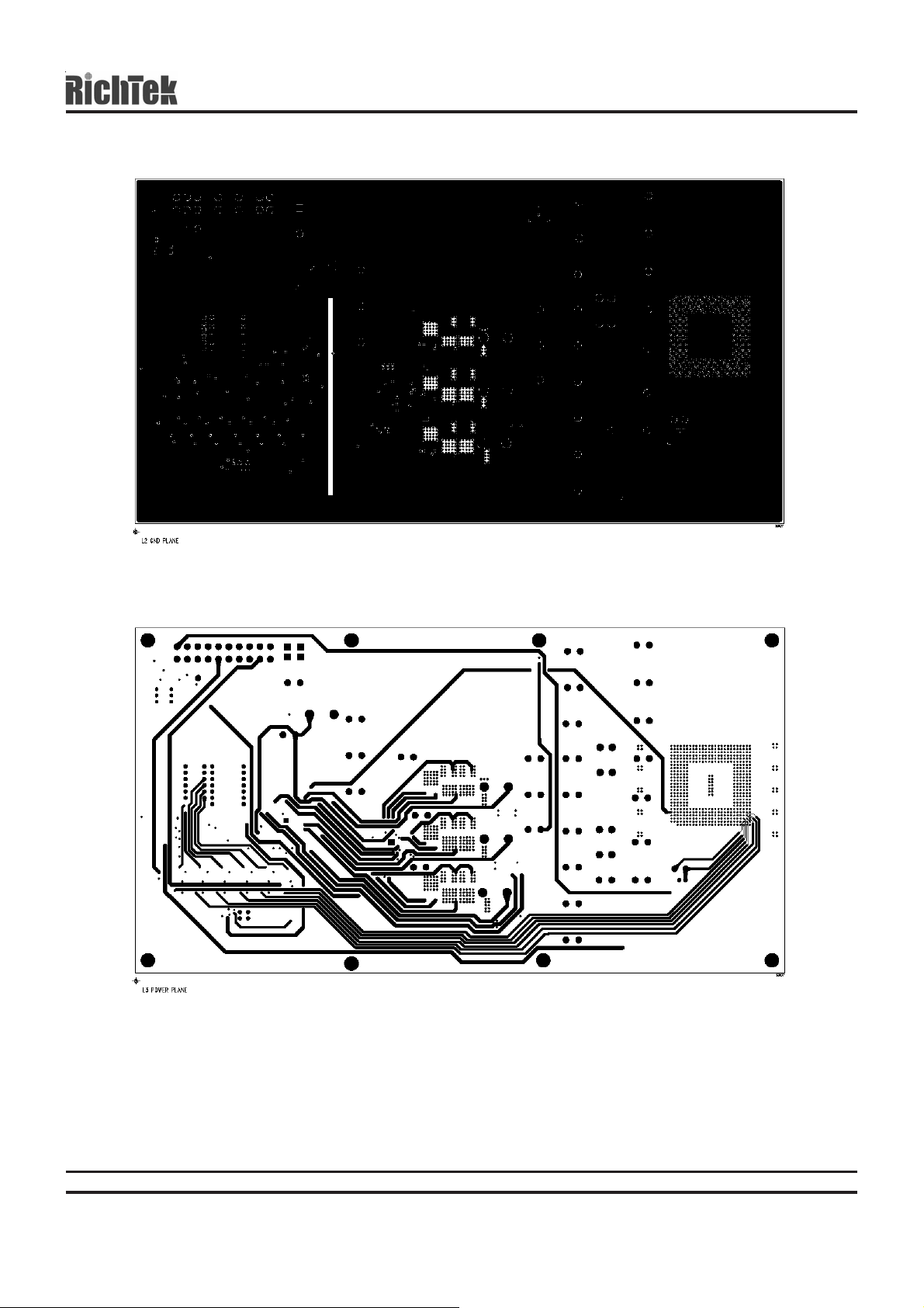
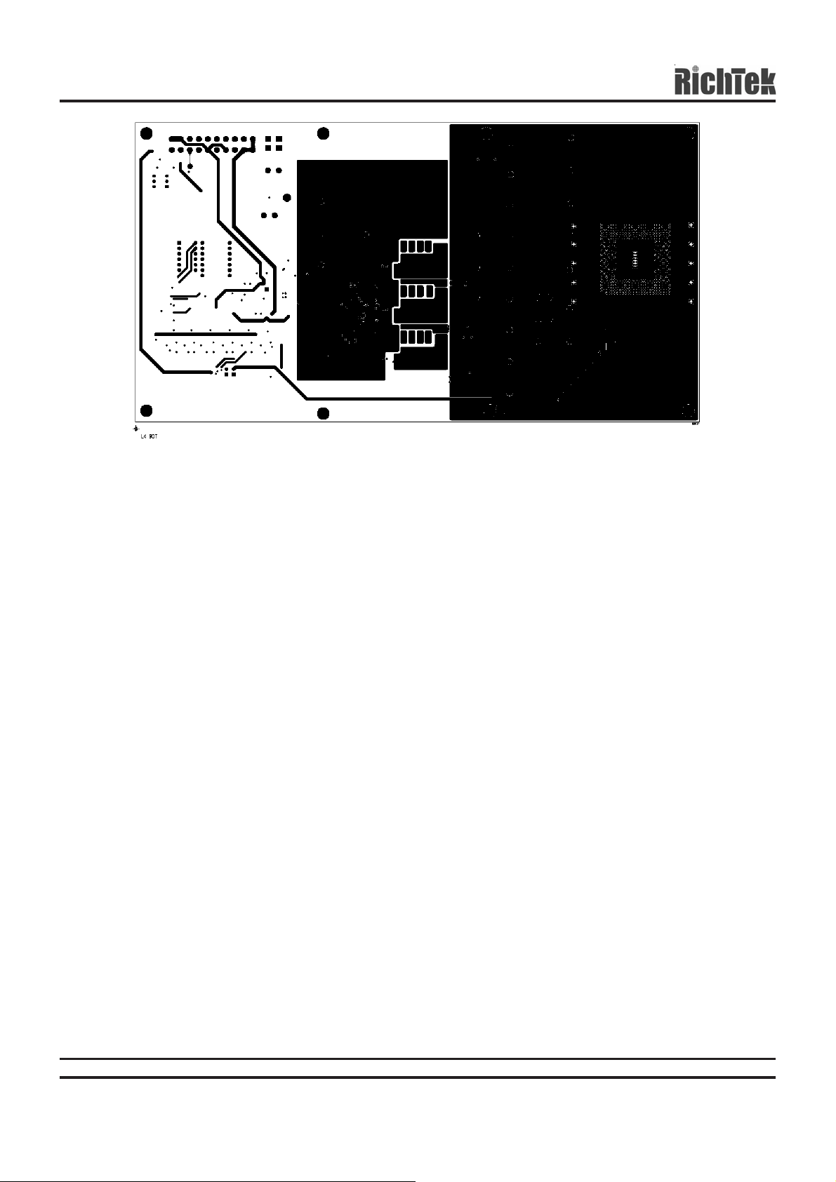
Layout Guide
Place the high-power switching components first, a nd separate them from sensitive nodes.
1. Most critical path:
The current sense circuit is the most sensitive part of the converter . The current sense resistors tied to ISP1,2,3 a nd
ICOMMON should be located not more tha n 0.5 inch from the IC and away from the noise switching nodes. The PCB
trace of sense nodes should be parallel a nd a s short a s possible. R&C filter of choke should place close to PWM a nd
the R & C connect directly to the pin of each output choke, use 10 mil dif ferencial pair , a nd 20 mil ga p to other pha se
pair. Less vi a as possible.
2. Switching ripple current path:
a. Input ca pa citor to high side MOSFET.
b. Low side MOSFET to output ca pa citor.
c. The return path of input and output capa citor .
d. Separate the power and signal GND.
e. The switching nodes (the connection node of high/low side MOSFET a nd inductor) is the most noisy points.Keep
them away from sensitive small-signal node.
f . Reduce parasitic R, L by mini mum length, enough copper thickness a nd avoiding of vi a.
3. MOSFET driver should be closed to MOSFET.
V
IN
R
IN
C
V
IN
SW1
SW2
L1
V
OUT
C
OUT
L2
R
L
Figure 22. Power Stage Ripple Current Path
All brand name or trademark belong to their owner respectively
DS8800/B-04 November 2005 www.richtek.com
21
RT8800/B
+12V
0.1uF
VCC
IN
BST
DRVH
SW
RT9603
DRVL
GND
Locate near MOSFETs
Next to IC
C
C
IN
BOOT
+12V or +5V
L
O1
V
CORE
C
OUT
R
ICOM
Figure 23. Layout Consideration
PWM
RT
GND
RT8800/B
ICOMMON
CSPx
GND
VCC
COMP
FB
PI
C
C
R
R
C
FB
BP
R
C
DRD
+5V
IN
Next to IC
Locate next
to FB Pin
22
Figure 24
All brand name or trademark belong to their owner respectively
DS8800/B-04 November 2005www.richtek.com
RT8800/B
Figure 25
Figure 26
All brand name or trademark belong to their owner respectively
DS8800/B-04 November 2005 www.richtek.com
23
RT8800/B
Figure 27
24
All brand name or trademark belong to their owner respectively
DS8800/B-04 November 2005www.richtek.com
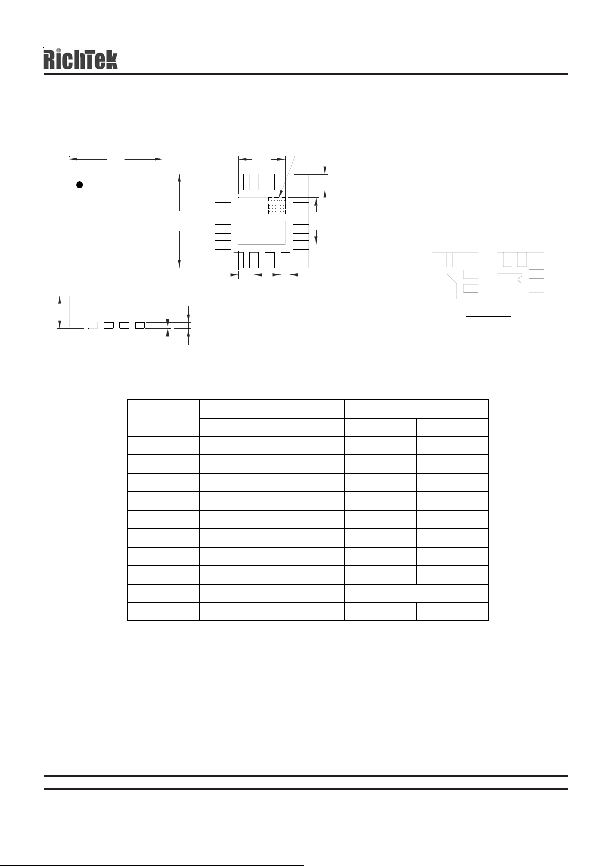
Outline Dimension
RT8800/B
D
E
A
A3
A1
D2
e
SEE DETAIL A
1
E2
b
L
1
2
1
2
DETAIL A
Pin #1 ID a nd T ie Bar Mark Option s
Note : The configuration of the Pin #1 identifier is optional,
but must be located within the zone indicated.
Dimensions In Millimeters Dimensions In Inches
Symbol
Min Max Min Max
A 0.800 1.000 0.031 0.039
A1 0.000 0.050 0.000 0.002
A3 0.175 0.250 0.007 0.010
b 0.180 0.300 0.007 0.012
D 2.950 3.050 0.116 0.120
D2 1.300 1.750 0.051 0.069
E 2.950 3.050 0.116 0.120
E2 1.300 1.750 0.051 0.069
e 0.500 0.020
L 0.350 0.450
0.014 0.018
V-Type 16L QFN 3x3 Package
All brand name or trademark belong to their owner respectively
DS8800/B-04 November 2005 www.richtek.com
25

RT8800/B
A
J
I
B
F
C
D
H
M
Dimensions In Millimeters Dimensions In Inches
Symbol
Min Max Min Max
A 9.804 10.008 0.386 0.394
B 3.810 3.988 0.150 0.157
C 1.346 1.753 0.053 0.069
D 0.330 0.508 0.013 0.020
F 1.194 1.346 0.047 0.053
H 0.178 0.254 0.007 0.010
I 0.102 0.254 0.004 0.010
J 5.791 6.198 0.228 0.244
M 0.406 1.270 0.016 0.050
RICHTEK TECHNOLOGY CORP .
Headquarter
5F, No. 20, Taiyuen Street, Chupei City
Hsinchu, Taiwan, R.O.C.
Tel: (8863)5526789 Fax: (8863)5526611
All brand name or trademark belong to their owner respectively
16–Lead SOP Plastic Package
RICHTEK TECHNOLOGY CORP .
Taipei Office (Marketing)
8F-1, No. 137, Lane 235, Paochiao Road, Hsintien City
Taipei County, Taiwan, R.O.C.
Tel: (8862)89191466 Fax: (8862)89191465
Email: marketing@richtek.com
26
DS8800/B-04 November 2005www.richtek.com
 Loading...