


QUICK LOGIC QL6500-4PS672M, QL6500-4PT280C, QL6500-4PT280I, QL6500-4PT280M, QL6500-5PB516C Datasheet
...QL6500 Eclipse Data Sheet
• • • • • • Combining Performance, Density and Embedded RAM
Device Highlights
Flexible Programmable Logic
•.25 m, Five layer metal CMOS Process
•2.5 V VCC, 2.5 V/3.3 V Drive Capable I/O
•3,032 Logic Cells
•488,064 Max System Gates
•Up to 444 I/O Pins
Embedded Dual Port SRAM
•Thirty six 2,304-bit Dual Port High Performance SRAM Blocks
•82,900 RAM Bits
•RAM/ROM/FIFO Wizard for Automatic Configuration
•Configurable and Cascadable
Programmable I/O
Advanced Clock Network
•Nine Global Clock Networks:
•One Dedicated
•Eight Programmable
•20 Quad-Net Networks: Five per Quadrant
•16 I/O Controls: Two per I/O Bank
Memory - Dual Port RAM
High Speed Logic Cells
488K Gates
Memory - Dual Port RAM
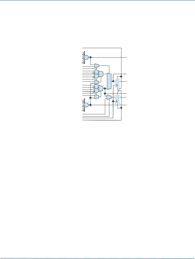
Figure 1: Eclipse Block Diagram
•High performance Enhanced I/O (EIO): Less than 3 ns Tco
•Programmable Slew Rate Control
•Programmable I/O Standards:
•LVTTL, LVCMOS, PCI, GTL+, SSTL2, and SSTL3
•Eight Independent I/O Banks
•Three Register Configurations: Input, Output, and Output Enable
•
•
© 2002 QuickLogic Corporation www.quicklogic.com •• 1
•
•
QL6500 Eclipse Data Sheet Rev C
Electrical Specifications
AC Characteristics at VCC = 2.5 V, TA = 25° C (K = 0.74)
The AC Specifications are provided from Table 1 to Table 10. Logic Cell diagrams and waveforms are provided from Figure 2 to Figure 15.
Figure 2: Eclipse Logic Cell
|
Table 1: Logic Cells |
|
|
|
|
|
|
|
|
Symbol |
Parameter |
Value (ns) |
||
Logic Cells |
|
Min |
|
Max |
|
|
|||
|
|
|
|
|
tPD |
Combinatorial Delay of the longest path: time taken by the combinatorial circuit to |
- |
|
0.257 |
output |
|
|||
|
|
|
|
|
|
|
|
|
|
tSU |
Setup time: time the synchronous input of the flip-flop must be stable before the |
0.22 |
|
- |
active clock edge |
|
|||
|
|
|
|
|
|
|
|
|
|
tHL |
Hold time: time the synchronous input of the flip-flop must be stable after the active |
0 |
|
- |
clock edge |
|
|||
|
|
|
|
|
|
|
|
|
|
tCO |
Clock to out delay: the amount of time taken by the flip-flop to output after the |
- |
|
0.255 |
active clock edge. |
|
|||
|
|
|
|
|
|
|
|
|
|
tCWHI |
Clock High Time: required minimum time the clock stays high |
0.46 |
|
- |
tCWLO |
Clock Low Time: required minimum time that the clock stays low |
0.46 |
|
- |
tSET |
Set Delay: time between when the flip-flop is ”set” (high) |
- |
|
0.18 |
and when the output is consequently “set” (high) |
|
|||
|
|
|
|
|
|
|
|
|
|
tRESET |
Reset Delay: time between when the flip-flop is ”reset” (low) and when the output |
- |
|
0.09 |
is consequently “reset” (low) |
|
|||
|
|
|
|
|
|
|
|
|
|
tSW |
Set Width: time that the SET signal remains high/low |
0.3 |
|
- |
tRW |
Reset Width: time that the RESET signal remains high/low |
0.3 |
|
- |
|
• |
|
2 |
• |
© 2002 QuickLogic Corporation |
• www.quicklogic.com |
||
|
• |
|
|
• |
|
|
• |
|
QL6500 Eclipse Data Sheet Rev C
SET
D
Q
CLK
RESET
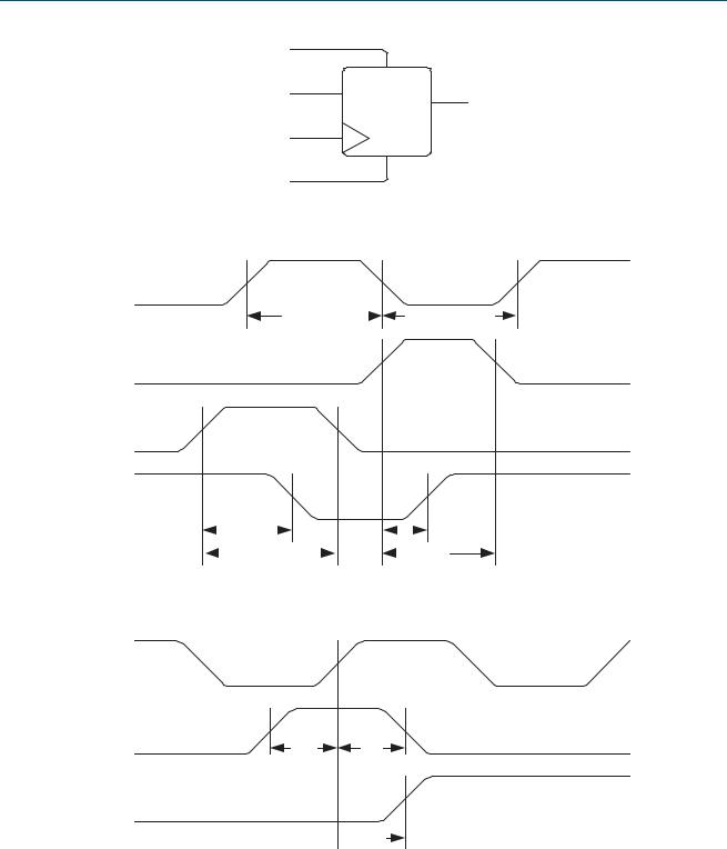
Figure 3: Logic Cell Flip Flop
CLK
tCWHI (min) |
|
tCWLO (min) |
|
SET
RESET
Q
|
|
tRESET |
|
|
|
|
|
|
|
|
|
|
|
|
|
|
|
|
tSET |
||||||
|
|
|
tRW |
|
|
|
|
|
|
|
tSW |
|
|
|
|
|
|
|
|
|
|||||
Figure 4: Logic Cell Flip Flop Timings - First Waveform
CLK
D |
tSU |
tHL |
|
Q
 tCO
tCO
Figure 5: Logic Cell Flip Flop Timings - Second Waveform
|
|
|
• |
© 2002 QuickLogic Corporation |
www.quicklogic.com |
• |
|
• 3 |
|||
|
|
|
• |
|
|
|
• |
|
|
|
• |

QL6500 Eclipse Data Sheet Rev C
Quad net
Figure 6: Eclipse Global Clock Structure
Table 2: Eclipse Clock Performance
Clock |
Parameters |
Clock Performance |
|||
|
|
Global |
|
Dedicated |
|
|
|
|
|||
|
|
|
|
|
|
Logic Cells (Internal) |
Clock signal generated internally |
1.51 ns (max) |
|
1.59 ns (max) |
|
|
|
|
|
|
|
I/O’s (External) |
Clock signal generated externally |
2.06 ns (max) |
|
1.73 ns (max) |
|
|
|
|
|
|
|
|
Table 3: Eclipse Global Clock Performance |
|
|
||
|
|
|
|
|
|
Clock Segment |
Parameter |
Value (ns) |
|||
|
|
Min |
|
|
Max |
|
|
|
|
||
|
|
|
|
|
|
tPGCK |
Global clock pin delay to quad net |
- |
|
1.34 |
|
tBGCK |
Global clock buffer delay |
- |
|
0.56 |
|
(quad net to flip flop) |
|
||||
|
|
|
|
|
|
|
|
|
|
|
|
Programmable Clock
External Clock
tPGCK
Global Clock Buffer

 Global Clock
Clock
Select
tBGCK
Figure 7: Global Clock Structure Schematic
•
•
4 • www.quicklogic.com © 2002 QuickLogic Corporation
•
•
•
QL6500 Eclipse Data Sheet Rev C
[9:0] |
RE |
WA |
|
[17:0] |
RCLK |
WD |
|
WE |
[9:0] |
RA |
|
|
[17:0] |
WCLK |
RD |
|
ASYNCRD |
RAM Module |
|
Figure 8: RAM Module |
|
Table 4: RAM Cell Synchronous Write Timing
Symbol |
Parameter |
Value (ns) |
||
|
|
|
|
|
RAM Cell Synchronous Write Timing |
Min |
Max |
||
|
|
|
|
|
tSWA |
WA setup time to WCLK: time the WRITE ADDRESS must be stable before the |
0.675 |
- |
|
active edge of the WRITE CLOCK |
||||
|
|
|
||
|
|
|
|
|
tHWA |
WA hold time to WCLK: time the WRITE ADDRESS must be stable after the active |
0 |
- |
|
edge of the WRITE CLOCK |
||||
|
|
|
||
|
|
|
|
|
tSWD |
WD setup time to WCLK: time the WRITE DATA must be stable before the active |
0.654 |
- |
|
edge of the WRITE CLOCK |
||||
|
|
|
||
|
|
|
|
|
tHWD |
WD hold time to WCLK: time the WRITE DATA must be stable after the active edge |
0 |
- |
|
of the WRITE CLOCK |
||||
|
|
|
||
|
|
|
|
|
tSWE |
WE setup time to WCLK: time the WRITE ENABLE must be stable before the active |
0.623 |
- |
|
edge of the WRITE CLOCK |
||||
|
|
|
||
|
|
|
|
|
tHWE |
WE hold time to WCLK: time the WRITE ENABLE must be stable after the active |
0 |
- |
|
edge of the WRITE CLOCK |
||||
|
|
|
||
|
|
|
|
|
tWCRD |
WCLK to RD (WA = RA): time between the active WRITE CLOCK edge and the |
- |
4.38 |
|
time when the data is available at RD |
||||
|
|
|
||
|
|
|
|
|
|
|
|
• |
© 2002 QuickLogic Corporation |
www.quicklogic.com |
• |
|
• 5 |
|||
|
|
|
• |
|
|
|
• |
|
|
|
• |
QL6500 Eclipse Data Sheet Rev C
|
WCLK |
|
|
|
|
|
|
|
|
|
|
|
|
|
|
|
|
|
|
|
|
|
|
|
|
|
|
|
|
|
|
|
WA |
|
|
|
|
|
|
|
|
|
|
|
|
|
|
|
|
|
|
tSWA |
|
|
|
|
|
tHWA |
|
|
|
|
|
|
|
|
|
|
|
|
|
|
|
|
|
||||
|
WD |
|
|
|
|
|
|
|
|
|
|
|
|
|
|
|
|
|
|
tSWD |
|
|
|
tHWD |
|
|
|
|
|||
|
|
|
|
|
|
|
|
|
|
||||||
|
|
|
|
|
|
||||||||||
|
WE |
|
|
|
|
|
|
|
|
|
|
|
|
|
|
|
|
|
|
tSWE |
|
|
|
tHWE |
|
|
|
|
|||
|
|
|
|
|
|
|
|
|
|||||||
|
|
|
|
|
|
||||||||||
|
RD |
|
old data |
|
|
|
|
new data |
|
|
|||||
|
|
|
|
|
|
|
|
|
|
tWCRD |
|
|
|
|
|
|
|
|
|
|
|
|
|
|
|
|
|
|
|
|
|
|
Figure 9: RAM Cell Synchronous Write Timing |
|
|
||||||||||||
|
Table 5: RAM Cell Synchronous & Asynchronous Read Timing |
|
|
||||||||||||
|
|
|
|
|
|
|
|
|
|
|
|
|
|
|
|
Symbol |
|
|
|
Parameter |
|
|
|
|
|
Value (ns) |
|||||
|
|
|
|
|
|
|
|
|
|
|
|
|
|
|
|
RAM Cell Synchronous Read Timing |
|
|
|
|
|
|
|
|
|
|
|
Min |
Max |
||
|
|
|
|
|
|
|
|
|
|
|
|
|
|
|
|
tSRA |
RA setup time to RCLK: time the READ ADDRESS must be stable before the active |
0.686 |
- |
||||||||||||
edge of the READ CLOCK |
|
|
|
|
|
|
|
|
|
|
|
||||
|
|
|
|
|
|
|
|
|
|
|
|
|
|
||
|
|
|
|
|
|
|
|
|
|
|
|
|
|
|
|
tHRA |
RA hold time to RCLK: time the READ ADDRESS must be stable after the active |
0 |
- |
||||||||||||
edge of the READ CLOCK |
|
|
|
|
|
|
|
|
|
|
|
||||
|
|
|
|
|
|
|
|
|
|
|
|
|
|
||
|
|
|
|
|
|
|
|
|
|
|
|
|
|
|
|
tSRE |
RE setup time to WCLK: time the READ ENABLE must be stable before the active |
0.243 |
- |
||||||||||||
edge of the READ CLOCK |
|
|
|
|
|
|
|
|
|
|
|
||||
|
|
|
|
|
|
|
|
|
|
|
|
|
|
||
|
|
|
|
|
|
|
|
|
|
|
|
|
|
|
|
tHRE |
RE hold time to WCLK: time the READ ENABLE must be stable after the active |
0 |
- |
||||||||||||
edge of the READ CLOCK |
|
|
|
|
|
|
|
|
|
|
|
||||
|
|
|
|
|
|
|
|
|
|
|
|
|
|
||
|
|
|
|
|
|
|
|
|
|
|
|
|
|
|
|
tRCRD |
RCLK to RD: time between the active READ CLOCK edge and the time when the |
- |
4.38 |
||||||||||||
data is available at RD |
|
|
|
|
|
|
|
|
|
|
|
||||
|
|
|
|
|
|
|
|
|
|
|
|
|
|
||
|
|
|
|
|
|
|
|
|
|
|
|
|
|
|
|
RAM Cell Asynchronous Read Timing |
|
|
|
|
|
|
|
|
|
|
|
|
|
||
|
|
|
|
|
|
|
|
|
|
|
|
|
|
|
|
rPDRD |
RA to RD: time between when the READ ADDRESS is input and when the DATA |
- |
2.06 |
||||||||||||
is output |
|
|
|
|
|
|
|
|
|
|
|
||||
|
|
|
|
|
|
|
|
|
|
|
|
|
|
||
|
|
|
|
|
|
|
|
|
|
|
|
|
|
|
|
•
•
6 • www.quicklogic.com © 2002 QuickLogic Corporation
•
•
•
QL6500 Eclipse Data Sheet Rev C
RCLK
RA
|
tSRA |
tHRA |
RE |
|
|
|
tSRE |
tHRE |
RD |
old data |
new data |
 tRCRD
tRCRD 
rPDRD
Figure 10: RAM Cell Synchronous & Asynchronous Read Timing
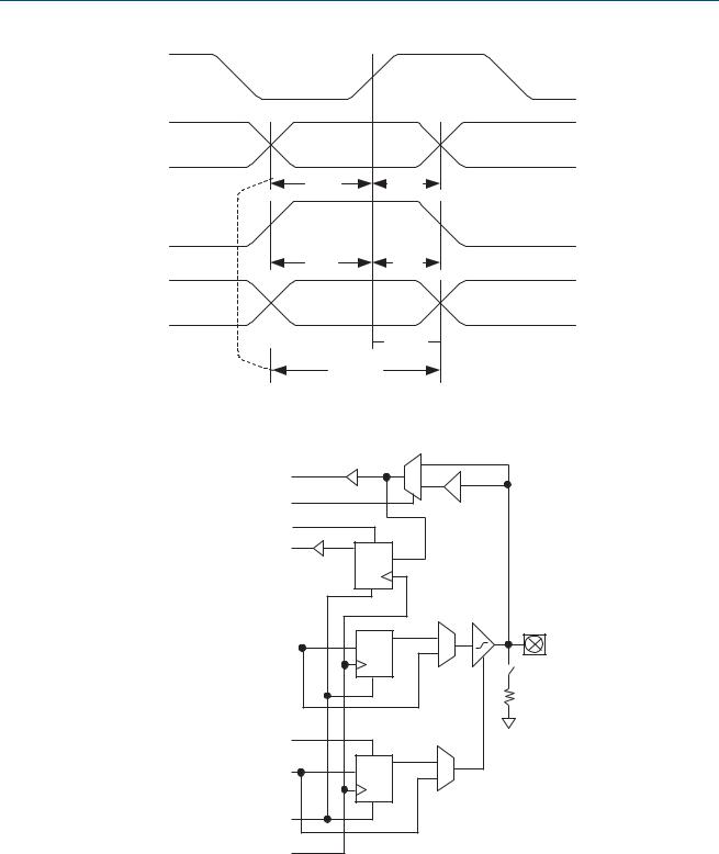
INPUT |
Q E |
|
REGISTER |
D |
|
|
R |
|
OUTPUT |
Q |
|
D |
||
|
||
REGISTER |
|
|
|
R |
|
OUTPUT ENABLE |
E Q |
|
D |
||
REGISTER |
|
|
|
R |
+
-
PAD
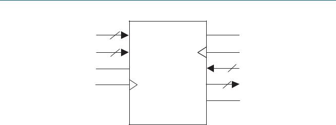
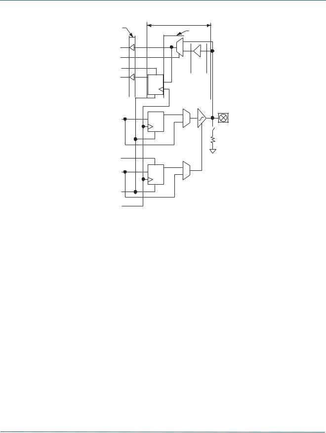
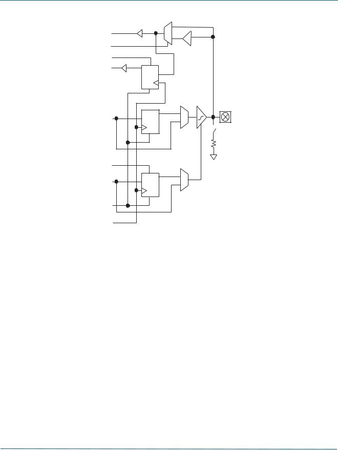
Figure 11: Eclipse Cell I/O
|
|
|
• |
© 2002 QuickLogic Corporation |
www.quicklogic.com |
• |
|
• 7 |
|||
|
|
|
• |
|
|
|
• |
|
|
|
• |
QL6500 Eclipse Data Sheet Rev C
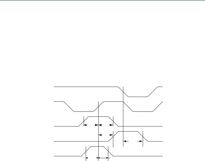
|
tICLK |
tIN, tINI |
tISU |
+
-
tSID
Q E
D
R
PAD
Figure 12: Eclipse Input Register Cell
Table 6: Input Register Cell
Symbol |
Parameter |
Value (ns) |
||
|
|
|
|
|
Input Register Cell Only |
Min |
Max |
||
|
|
|
|
|
tISU |
Input register setup time: time the synchronous input of the flip-flop must be stable |
3.12 |
- |
|
before the active clock edge |
||||
|
|
|
||
|
|
|
|
|
tIHL |
Input register hold time: time the synchronous input of the flip-flop must be stable |
0 |
- |
|
after the active clock edge |
||||
|
|
|
||
|
|
|
|
|
tICO |
Input register clock to out: time taken by the flip-flop to output after the active clock |
- |
1.08 |
|
edge |
||||
|
|
|
||
|
|
|
|
|
tIRST |
Input register reset delay: time between when the flip-flop is “reset”(low) and when |
- |
0.99 |
|
the output is consequently “reset” (low) |
||||
|
|
|
||
|
|
|
|
|
tIESU |
Input register clock enable setup time: time “enable” must be stable before the |
0.37 |
- |
|
active clock edge |
||||
|
|
|
||
|
|
|
|
|
tIEH |
Input register clock enable hold time: time “enable” must be stable after the active |
0 |
- |
|
clock edge |
||||
|
|
|
||
|
|
|
|
|
•
•
8 • www.quicklogic.com © 2002 QuickLogic Corporation
•
•
•
QL6500 Eclipse Data Sheet Rev C
|
|
|
|
|
|
|
|
|
|
|
|
|
|
|
|
|
|
|
|
|
|
|
|
|
|
|
|
|
|
|
|
|
|
|
|
R |
|
|
|
|
CLK |
|
|
|
|
D |
|
|
|
|
tISU |
tIHL |
|
|
|
Q |
tICO |
|
|
|
E |
tIEH |
|
|
|
tIESU |
|
|
|
|
Table 7: Standard Input Delays |
|
|
|
Symbol |
|
Parameter |
Value (ns) |
|
Standard Input Delays |
To get the total input delay add this delay to tISU |
Min |
Max |
|
tSID (LVTTL) |
LVTTL input delay: Low Voltage TTL for 3.3 V applications |
- |
0.34 |
|
tSID (LVCMOS2) |
LVCMOS2 input delay: Low Voltage CMOS for 2.5 V and lower |
- |
0.42 |
|
|
applications |
|
|
|
tSID (GTL+) |
GTL+ input delay: Gunning Transceiver Logic |
- |
0.68 |
|
tSID (SSTL3) |
SSTL3 input delay: Stub Series Terminated Logic for 3.3 V |
- |
0.55 |
|
tSID (SSTL2) |
SSTL2 input delay: Stub Series Terminated Logic for 2.5 V |
- |
0.61 |
|
tIRST
Figure 13: Eclipse Input Register Cell Timing
|
|
|
• |
© 2002 QuickLogic Corporation |
www.quicklogic.com |
• |
|
• 9 |
|||
|
|
|
• |
|
|
|
• |
|
|
|
• |
QL6500 Eclipse Data Sheet Rev C
PAD
OUTPUT
REGISTER
Figure 14: Eclipse Output Register Cell
Table 8: Eclipse Output Register Cell
Symbol |
Parameter |
|
Value (ns) |
|
|
|
|
|
|
Output Register Cell Only |
Min |
|
Max |
|
|
|
|
|
|
tOUTLH |
Output Delay low to high (90% of H) |
- |
|
0.40 |
tOUTHL |
Output Delay high to low (10% of L) |
- |
|
0.55 |
tPZH |
Output Delay tri-state to high (90% of H) |
- |
|
2.94 |
tPZL |
Output Delay tri-state to low (10% of L) |
- |
|
2.34 |
tPHZ |
Output Delay high to tri-State |
- |
|
3.07 |
tPLZ |
Output Delay low to tri-State |
- |
|
2.53 |
tCOP |
Clock to out delay (does not include clock tree delays) |
- |
|
3.15 (fast slew) |
|
10.2 (slow slew) |
|||
|
|
|
|
|
|
|
|
|
|
•
•
10 • www.quicklogic.com © 2002 QuickLogic Corporation
•
•
•
QL6500 Eclipse Data Sheet Rev C
H |
|
|
|
|
|
|
|
|
|
|
|
|
|
|
|
|
|
|
|
|
|
|
|
|
|
|
|
tOUTHL |
|
|
|
|
|
|
|
|
|
|
|
|
|
H |
|
|
|
|
|
|
|||||||||
|
|
|
|
|
|
|
|
|
|
|
|
|
|
|
|
|
|
|
|
|
|
|
||||||
L |
|
|
|
|
|
|
|
|
|
|
|
|
|
|
|
|
|
|
|
|
|
|
|
|
|
|
|
|
|
|
|
|
|
|
|
|
|
|
|
|
tOUTLH |
L |
|
|
|
|
|
|
|||||||||
|
|
|
|
|
|
|
|
|
|
|
|
|
||||||||||||||||
H |
|
|
|
|
|
|
|
|
|
|
|
|
H |
|||||||||||||||
|
|
|
|
|
||||||||||||||||||||||||
|
|
|
|
|
|
|
|
|
|
|
|
|
||||||||||||||||
|
|
|
|
|
|
|
|
|
|
|
|
|
||||||||||||||||
Z |
|
|
|
|
|
|
|
|
|
|
|
|
|
|
|
|
|
|
|
|
|
|
|
|
|
|
|
tPZL |
|
|
|
|
|
|
|
|
|
|
|
|
|
|
|
|
|
|
|
|
|
|
|
|
|
|
|
||
|
|
|
|
|
|
|
|
|
|
tPZH |
Z |
|||||||||||||||||
L |
|
|
|
|
|
|
|
|
|
|
L |
|
|
|
|
|
|
|
tPHZ |
|||||||||
|
|
|
|
|
|
|
|
|
|
|
|
|
|
|
|
|
||||||||||||
|
|
|
|
|
|
|
|
|
|
|
|
|
|
|
|
|
||||||||||||
H |
|
|
|
|
|
|
|
|
|
|
|
|
|
|
|
|
|
|
|
|
|
|
|
|
||||
|
|
|
|
|
|
|
|
|
|
|
|
|
H |
|
|
|
|
|
|
|
||||||||
Z |
|
|
|
|
|
|
|
|
|
|
|
|
|
Z |
|
|
|
|
|
|||||||||
|
|
|
|
|
|
|
|
|
|
|
|
|
|
|||||||||||||||
|
|
|
|
|
|
|
|
|
|
|
|
|
|
|
|
|
|
|
|
|
|
|
|
|||||
L |
|
|
|
|
|
|
|
|
|
|
|
|
|
L |
||||||||||||||
|
|
|
|
|
|
|
|
tPLZ |
|
|
|
|
|
|
|
|
|
|
|
|
|
|
|
|||||
|
|
|
|
|
|
|
|
|
|
|
|
|
|
|
|
|
|
|
|
|
|
|
||||||
|
|
Figure 15: Eclipse Output Register Cell Timing |
||||||||||||||||||||||||||
|
|
|
|
Table 9: Output Slew Rates @ VCCIO = 3.3 V |
||||||||||||||||||||||||
|
|
|
|
|
|
|
|
|
|
|
|
|
|
|
|
|
|
|
|
|
|
|
|
|
|
|
|
|
|
|
|
|
|
|
|
|
|
|
|
Fast Slew |
|
|
|
|
|
|
|
|
|
|
Slow Slew |
||||||
|
|
|
|
|
|
|
|
|
|
|
|
|
|
|
|
|
|
|
|
|
|
|
|
|
|
|
|
|
Rising Edge |
|
|
|
|
|
|
|
|
|
|
2.8 V/ns |
|
|
|
|
|
|
|
|
|
|
|
1.0 V/ns |
|||||
|
|
|
|
|
|
|
|
|
|
|
|
|
|
|
|
|
|
|
|
|
|
|
|
|
|
|
|
|
Falling Edge |
|
|
|
|
|
|
|
|
|
|
2.86 V/ns |
|
|
|
|
|
|
|
|
|
|
|
1.0 V/ns |
|||||
|
|
|
|
|
|
|
|
|
|
|
|
|
|
|
|
|
|
|
|
|
|
|
|
|
|
|
|
|
|
|
|
|
Table 10: Output Slew Rates @ VCCIO = 2.5 V |
||||||||||||||||||||||||
|
|
|
|
|
|
|
|
|
|
|
|
|
|
|
|
|
|
|
|
|
|
|
|
|
|
|
|
|
|
|
|
|
|
|
|
|
|
|
|
Fast Slew |
|
|
|
|
|
|
|
|
|
|
Slow Slew |
||||||
|
|
|
|
|
|
|
|
|
|
|
|
|
|
|
|
|
|
|
|
|
|
|
|
|
|
|
|
|
Rising Edge |
|
|
|
|
|
|
|
|
|
|
1.7 V/ns |
|
|
|
|
|
|
|
|
|
|
|
0.6 V/ns |
|||||
|
|
|
|
|
|
|
|
|
|
|
|
|
|
|
|
|
|
|
|
|
|
|
|
|
|
|
|
|
Falling Edge |
|
|
|
|
|
|
|
|
|
|
1.9 V/ns |
|
|
|
|
|
|
|
|
|
|
|
0.6 V/ns |
|||||
|
|
|
|
|
|
|
|
|
|
|
|
|
|
|
|
|
|
|
|
|
|
|
|
|
|
|
|
|
|
|
|
• |
© 2002 QuickLogic Corporation |
www.quicklogic.com |
• |
|
• 11 |
|||
|
|
|
• |
|
|
|
• |
|
|
|
• |

QL6500 Eclipse Data Sheet Rev C
DC Characteristics
The DC Specifications are provided in Table 11 through Table 13.
Table 11: Absolute Maximum Ratings
|
Parameter |
|
|
Value |
|
|
|
|
Parameter |
|
|
|
|
Value |
|
|
|||
|
|
|
|
|
|
|
|
|
|
|
|
|
|
|
|
|
|
||
|
VCC Voltage |
|
|
-0.5 V to 3.6 V |
|
|
|
DC Input Current |
|
|
±20 mA |
|
|
||||||
|
|
|
|
|
|
|
|
|
|
|
|
|
|
|
|
|
|
||
|
VCCIO Voltage |
|
|
-0.5 V to 4.6 V |
|
|
|
ESD Pad Protection |
|
|
±2000 V |
|
|
||||||
|
|
|
|
|
|
|
|
|
|
|
|
|
|
|
|
|
|
||
|
INREF Voltage |
|
|
2.7 V |
|
|
|
Leaded Package |
-65° C to + 150° C |
||||||||||
|
|
|
|
|
|
Storage Temperature |
|||||||||||||
|
|
|
|
|
|
|
|
|
|
|
|
|
|
||||||
|
|
|
|
|
|
|
|
|
|
|
|
|
|
|
|
|
|
||
|
Input Voltage |
|
-0.5 V to VCCIO +0.5 V |
|
|
Laminate Package (BGA) |
-55° C to + 125° C |
||||||||||||
|
Latch-up Immunity |
|
|
±100 mA |
|
|
|
Storage Temperature |
|||||||||||
|
|
|
|
|
|
|
|
|
|
|
|||||||||
|
|
|
|
|
|
|
|
|
|
|
|
|
|
|
|
|
|||
|
|
|
|
|
|
|
|
|
|
|
|
|
|
|
|
|
|
||
|
|
|
|
|
Table 12: Operating Range |
|
|
|
|
|
|
|
|||||||
|
|
|
|
|
|
|
|
|
|
|
|
|
|
|
|
||||
|
Symbol |
|
Parameter |
Military |
|
Industrial |
|
Commercial |
Unit |
|
|||||||||
|
|
|
|
|
|
Min |
|
Max |
|
Min |
|
Max |
|
Min |
|
Max |
|
|
|
|
|
|
|
|
|
|
|
|
|
|
|
|
|||||||
|
|
|
|
|
|
|
|
|
|
|
|
|
|
|
|
|
|
|
|
|
VCC |
Supply Voltage |
2.3 |
|
2.7 |
|
2.3 |
|
2.7 |
|
2.3 |
|
2.7 |
V |
|||||
|
VCCIO |
I/O Input Tolerance Voltage |
2.3 |
|
3.6 |
|
2.3 |
|
3.6 |
|
2.3 |
|
3.6 |
V |
|
||||
|
TA |
Ambient Temperature |
-55 |
|
|
|
-40 |
|
85 |
|
0 |
|
70 |
°C |
|||||
|
|
|
|
|
|
|
|
|
|
|
|
|
|
|
|
|
|
||
|
TC |
Case Temperature |
- |
|
|
125 |
|
- |
|
- |
|
- |
|
- |
°C |
|
|||
|
|
|
|
|
|
|
|
|
|
|
|
|
|
|
|
|
|
|
|
|
|
|
|
|
-4 Speed Grade |
0.42 |
|
2.3 |
|
0.43 |
|
2.16 |
|
0.47 |
|
2.11 |
n/a |
||
|
|
|
|
|
|
|
|
|
|
|
|
|
|
|
|
|
|
|
|
|
K |
Delay Factor |
-5 Speed Grade |
0.42 |
|
1.92 |
|
0.43 |
|
1.80 |
|
0.46 |
|
1.76 |
n/a |
|
|||
|
|
|
|
|
|
|
|
|
|
|
|
|
|
|
|
||||
|
-6 Speed Grade |
0.42 |
|
1.35 |
|
0.43 |
|
1.26 |
|
0.46 |
|
1.23 |
n/a |
||||||
|
|
|
|
|
|
|
|
|
|
||||||||||
|
|
|
|
|
|
|
|
|
|
|
|
|
|
|
|
|
|
|
|
|
|
|
|
|
-7 Speed Grade |
0.42 |
|
1.27 |
|
0.43 |
|
1.19 |
|
0.46 |
|
1.16 |
n/a |
|
|
|
|
|
|
|
|
|
|
|
|
|
|
|
|
|
|
|
|
|
|
Table 13: DC Characteristics
Symbol |
Parameter |
|
Conditions |
Min |
Max |
Units |
|||
|
|
|
|
|
|
|
|||
|
II |
I or I/O Input Leakage Current |
VI = VCCIO or GND |
-10 |
10 |
µA |
|||
|
|
|
|
|
|
||||
IOZ |
3-State Output Leakage Current |
VI = VCCIO or GND |
-10 |
10 |
µA |
||||
CI |
Input Capacitancea |
|
|
- |
|
- |
8 |
pF |
|
|
|
|
|
|
|
|
|||
I |
Output Short Circuit Currentb |
|
Vo = GND |
-15 |
-180 |
mA |
|||
|
OS |
|
|
Vo = VCC |
40 |
210 |
mA |
||
|
|
|
|
||||||
I |
CC |
D.C. Supply Currentc |
V |
V = V |
CCIO |
or GND |
0.50 (typ) |
2 |
mA |
|
|
I, |
o |
|
|
|
|
||
ICCIO |
D.C. Supply Current on VCCIO |
|
|
- |
|
0 |
2 |
mA |
|
ICCIO(DIF) |
D.C. Supply Current on VCCIO |
|
|
- |
|
- |
- |
mA |
|
for Differential I/O |
|
|
|
||||||
|
|
|
|
|
|
|
|
|
|
|
|
|
|
|
|
|
|
|
|
IREF |
D.C. Supply Current on INREF |
|
|
- |
|
-10 |
10 |
µA |
|
IPD |
Pad Pull-down (programmable) |
|
VCCIO = 3.6 V |
- |
150 |
µA |
|||
a.Capacitance is sample tested only. Clock pins are 12 pF maximum.
b.Only one output at a time. Duration should not exceed 30 seconds.
c.For -4/-5/-6/-7 commercial grade devices only. Maximum ICC is 3 mA for -0 commercial grade and all industrial grade devices, and 5 mA for all military grade devices.
•
•
12 • www.quicklogic.com © 2002 QuickLogic Corporation
•
•
•
 Loading...