


QUICK LOGIC QL6250-E-6PQ208I, QL6250-E-6PQ208M, QL6250-E-6PS484C, QL6250-E-6PS484I, QL6250-E-6PS484M Datasheet
...-./012 ' 2
) # " " * " + " ,+ "
0.18 µm six layer metal CMOS Process
1.8/2.5/3.3 V Drive Capable I/O
960 Logic Cells
248,160 Max System Gates
Up to 250 I/O Pins
Twenty 2,304-bit Dual Port High Performance SRAM Blocks
46,100 RAM bits
RAM/ROM/FIFO Wizard for Automatic Configuration
Configurable and Cascadable
!
High performance Enhanced I/O (EIO)— less than 3 ns Tco
Programmable Slew Rate Control
Programmable I/O Standards:
LVTTL, LVCMOS, PCI, GTL+, SSTL2, and SSTL3
Eight Independent I/O Banks
Three Register Configurations: Input, Output, and Output Enable
" #$% &$
Nine Global Clock Networks:
One Dedicated
Eight Programmable
20 Quad-Net Networks—five per Quadrant
16 I/O Controls—two per I/O Bank
Four phase locked loops
# ' " ("
10 ECUs provide integrated Multiply, Add, and Accumulate Functions.
PLL |
Embedded RAM Blocks |
PLL |
|
10 Embeded Computational Units |
|
|
Fabric |
|
PLL |
Embedded RAM Blocks |
PLL |
|
|
|
|
|
|
Preliminary

' * "
# # 3
*(at VCC = 2.5 V, TA = 25° C, Worst Case Corner, Speed Grade = -7 (K = 1.16))
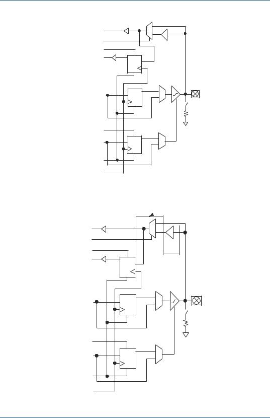
The AC Specifications are provided from 4 to 4 1. Logic Cell diagrams and waveforms are provided from / to 0.
, |
|
5 |
||
# |
|
" |
|
|
|
|
|||
|
|
|
|
|
tPD |
Combinatorial Delay of the longest path: time taken by the combinatorial circuit to |
- |
|
0.257 ns |
output |
|
|||
tSU |
Setup time: time the synchronous input of the flip-flop must be stable before the |
0.22 ns |
|
- |
active clock edge |
|
|||
tHL |
Hold time: time the synchronous input of the flip-flop must be stable after the active |
0 ns |
|
- |
clock edge |
|
|||
tCO |
Clock-to-out delay: the amount of time taken by the flip-flop to output after the |
- |
|
0.255 ns |
active clock edge. |
|
|||
tCWHI |
Clock High Time: required minimum time the clock stays high |
0.46 ns |
|
- |
tCWLO |
Clock Low Time: required minimum time that the clock stays low |
0.46 ns |
|
- |
tSET |
Set Delay: time between when the flip-flop is ”set” (high) |
- |
|
0.18 ns |
and when the output is consequently “set” (high) |
|
|||
/ Preliminary
, |
|
5 |
||
# |
|
" |
|
|
|
|
|||
|
|
|
|
|
tRESET |
Reset Delay: time between when the flip-flop is ”reset” (low) and when the output |
- |
|
0.09 ns |
is consequently “reset” (low) |
|
|||
tSW |
Set Width: time that the SET signal remains high/low |
0.3 ns |
|
- |
tRW |
Reset Width: time that the RESET signal remains high/low |
0.3 ns |
|
- |
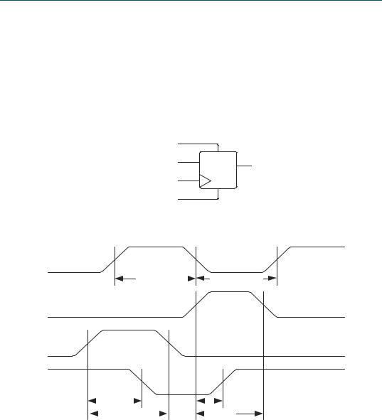
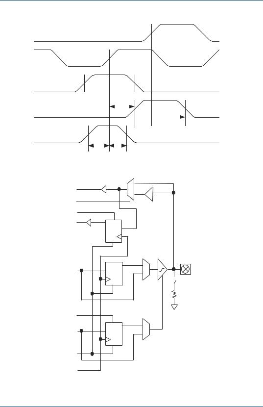
SET
D
Q
CLK
RESET
CLK
tCWHI (min) |
|
tCWLO (min) |
|
SET
RESET
Q
|
|
tRESET |
|
|
|
|
|
|
|
|
|
|
|
|
|
|
|
|
tSET |
||||||
|
|
|
tRW |
|
|
|
|
|
tSW |
|||
|
|
|
|
|
|
|
||||||
! " #$%
|
Preliminary |
|
|
|
6 |
||
|
|
|
|
|
|
|
||
|

CLK |
|
|
D |
tSU |
tHL |
|
Q
 tCO
tCO 
!& ' #$%
Quad net
( ) &" "
#$ |
|
#$* " |
||
|
|
) |
|
|
|
|
|
||
|
|
|
|
|
Logic Cells (Internal) |
Clock signal generated internally |
1.51 ns (max) |
|
|
|
|
|
|
|
Clock Pad |
Clock signal generated externally |
2.06 ns (max) |
|
1.73 ns (max) |
|
|
|
|
|
7 Preliminary
! "
#$" |
|
|
5 |
|
|
|
" |
|
|
|
|
|
||
|
|
|
|
|
a |
Global clock pin delay to quad net |
- |
|
1.34 ns |
tPGCK |
|
|||
tBGCK |
Global clock tree delay (quad net to |
- |
|
0.56 ns |
flip-flop) |
|
|||
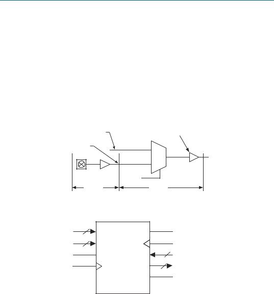
#$% &%" ' (" ' ) ** + , ) -
%$
Programmable Clock |
Global Clock Buffer |
External Clock
|
Global Clock |
|
Clock |
|
Select |
tPGCK |
tBGCK |
* ( ) &" " & + " |
|
[9:0] |
|
WA |
RE |
[17:0] |
RCLK |
WD |
|
|
[9:0] |
WE |
RA |
|
[17:0] |
WCLK |
RD |
|
ASYNCRD |
RAM Module |
|
,-./ / '
. /01 2 $) #)
|
|
5 |
||
, |
|
" |
|
|
|
||||
|
|
|
||
|
|
|
|
|
tSWA |
WA setup time to WCLK: time the WRITE ADDRESS must be stable before the |
0.675 ns |
|
- |
active edge of the WRITE CLOCK |
|
|||
tHWA |
WA hold time to WCLK: time the WRITE ADDRESS must be stable after the active |
0 ns |
|
- |
edge of the WRITE CLOCK |
|
|||
tSWD |
WD setup time to WCLK: time the WRITE DATA must be stable before the active |
0.654 ns |
|
- |
edge of the WRITE CLOCK |
|
|||
|
Preliminary |
|
|
|
0 |
||
|
|
|
|
|
|
|
||
|
. /01 2 $) #)
|
|
5 |
||
, |
|
" |
|
|
|
||||
|
|
|
||
|
|
|
|
|
tHWD |
WD hold time to WCLK: time the WRITE DATA must be stable after the active edge |
0 ns |
|
- |
of the WRITE CLOCK |
|
|||
tSWE |
WE setup time to WCLK: time the WRITE ENABLE must be stable before the active |
0.623 ns |
|
- |
edge of the WRITE CLOCK |
|
|||
tHWE |
WE hold time to WCLK: time the WRITE ENABLE must be stable after the active |
0 ns |
|
- |
edge of the WRITE CLOCK |
|
|||
tWCRD |
WCLK to RD (WA = RA): time between the active WRITE CLOCK edge and the |
- |
|
4.38 ns |
time when the data is available at RD |
|
|||
|
WCLK |
|
|
|
|
|
|
|
|
|
|
|
|
|
|
|
WA |
|
|
|
|
|
|
|
|
|
|
|
|
|
|
|
|
|
|
|
|
|
|
|
|
|
|
|
|
|
|
|
WD |
|
|
tSWA |
|
|
|
|
|
tHWA |
|
|
|
|
|
|
|
|
|
|
|
|
|
|
|
|
|||||
|
|
|
|
|
|
|
|
|
|
|
|
|
|
|
|
|
WE |
|
|
tSWD |
|
|
|
tHWD |
|
|
|
|
|||
|
|
|
|
|
|
|
|
|
|||||||
|
|
|
|
|
|
|
|
|
|
|
|
|
|
|
|
|
|
|
|
tSWE |
|
|
|
tHWE |
|
|
|
|
|||
|
|
|
|
|
|
|
|
|
|||||||
|
RD |
|
|
old data |
|
|
|
new data |
|
|
|
||||
|
|
|
|
|
|
|
|
|
|
tWCRD |
|
|
|
|
|
|
|
|
|
|
|
|
|
|
|
|
|
|
|
|
|
|
0-./ &1 + # " |
|
|
|
|||||||||||
|
3 /01 2 $) 4 0 $) / |
|
|
|
|||||||||||
|
|
|
|
|
|
|
|
|
|
|
|
|
|
|
|
|
# ," " 4 " |
5 |
|
||||||||||||
, |
|
|
|
|
|
|
" |
|
|
||||||
|
|
|
|
|
|
||||||||||
|
|
|
|
|
|
|
|||||||||
|
|
|
|
|
|
|
|
|
|
|
|
|
|
|
|
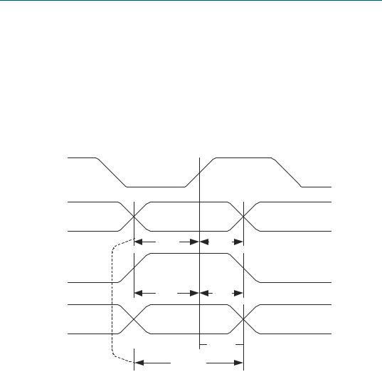
tSRA |
RA setup time to RCLK: time the READ ADDRESS must be stable before the active |
0.686 ns |
|
- |
|||||||||||
edge of the READ CLOCK |
|
|
|
|
|
|
|
|
|
|
|
|
|||
tHRA |
RA hold time to RCLK: time the READ ADDRESS must be stable after the active |
0 ns |
|
- |
|||||||||||
edge of the READ CLOCK |
|
|
|
|
|
|
|
|
|
|
|
|
|||
tSRE |
RE setup time to WCLK: time the READ ENABLE must be stable before the active |
0.243 ns |
|
- |
|||||||||||
edge of the READ CLOCK |
|
|
|
|
|
|
|
|
|
|
|
|
|||
tHRE |
RE hold time to WCLK: time the READ ENABLE must be stable after the active |
0 ns |
|
- |
|||||||||||
edge of the READ CLOCK |
|
|
|
|
|
|
|
|
|
|
|
|
|||
. |
Preliminary |
|
|
|
|
|
|
|
|
|
|
|
3 /01 2 $) 4 0 $) / |
|
|
|
|
|
|
|
|
|
# ," " 4 " |
|
5 |
|
, |
|
" |
|
|
|
||||
|
|
|||
|
|
|
|
|
tRCRD |
RCLK to RD: time between the active READ CLOCK edge and the time when the |
- |
|
4.38 ns |
data is available at RD |
|
|||
|
# ," " 4 " |
|
|
|
|
|
|
|
|
rPDRD |
RA to RD: time between when the READ ADDRESS is input and when the DATA |
- |
|
2.06 ns |
is output |
|
|||
RCLK
RA
|
tSRA |
tHRA |
RE |
|
|
|
tSRE |
tHRE |
RD |
old data |
new data |
 tRCRD
tRCRD 
rPDRD
-./ &1 + 2 . 1 + -'
|
Preliminary |
|
|
|
8 |
||
|
|
|
|
|
|
|
||
|
|
+ |
|
- |
INPUT |
Q E |
REGISTER |
D |
|
R |
|
PAD |
OUTPUT |
Q |
D |
|
REGISTER |
R |
|
|
OUTPUT ENABLE |
E Q |
D |
|
REGISTER |
R |
|
345
 tISU
tISU
+
-
tSID
Q E
D
R
PAD
3 "-"
9 Preliminary

5 6 / )
|
|
5 |
||
, |
; "' # !" , |
" |
|
|
|
||||
|
|
|
||
|
|
|
|
|
t |
Input register setup time: time the synchronous input of the flip-flop must be stable |
2.50 ns |
|
- |
ISU |
before the active clock edge |
|
|
|
|
|
|
|
|
tIHL |
Input register hold time: time the synchronous input of the flip-flop must be stable |
0 ns |
|
- |
after the active clock edge |
|
|||
tICO |
Input register clock-to-out: time taken by the flip-flop to output after the active clock |
- |
|
1.08 ns |
edge |
|
|||
tIRST |
Input register reset delay: time between when the flip-flop is “reset” (low) and when |
- |
|
0.99 ns |
the output is consequently “reset” (low) |
|
|||
tIESU |
Input register clock enable setup time: time “enable” must be stable before the |
0.37 ns |
|
- |
active clock edge |
|
|||
tIEH |
Input register clock enable hold time: time “enable” must be stable after the active |
0 ns |
|
- |
clock edge |
|
|||
7 2 ) 6
, |
|
5 |
||
" "' , |
4 "' , , ( |
" |
|
|
|
||||
|
|
|
|
|
tSID (LVTTL) |
LVTTL input delay: Low Voltage TTL for 3.3 V applications |
- |
|
0.34 ns |
tSID (LVCMOS2) |
LVCMOS2 input delay: Low Voltage CMOS for 2.5 V and lower |
- |
|
0.42 ns |
applications |
|
|||
|
|
|
|
|
tSID (LVCMOS18) |
LVCMOS18 input delay: Low Voltage CMOS for 1.8 V applications |
- |
|
- |
tSID (GTL+) |
GTL+ input delay: Gunning Transceiver Logic |
- |
|
0.68 ns |
tSID (SSTL3) |
SSTL3 input delay: Stub Series Terminated Logic for 3.3 V |
- |
|
0.55 ns |
tSID (SSTL2) |
SSTL2 input delay: Stub Series Terminated Logic for 2.5 V |
- |
|
0.61 ns |
|
Preliminary |
|
|
|
: |
||
|
|
|
|
|
|
|
||
|
R
CLK
D
 tISU
tISU  tIHL
tIHL 
Q |
tICO |
 tIRST
tIRST
E
tIESU tIEH
3 "-"
PAD
OUTPUT
REGISTER
5 " "-"
1 Preliminary
8 9 / )
|
, |
|
|
|
|
|
|
|
|
|
|
|
|
|
|
|
|
|
|
|
|
|
|
|
|
|
|
5 |
|
||||
|
|
|
|
|
|
|
|
|
|
|
|
|
|
|
|
|
|
|
|
|
|
|
|
|
|
|
|
|
|
|
|
|
|
|
! ' # !" , |
|
|
|
|
|
|
|
|
|
|
|
|
|
|
|
|
|
" |
|
|
|
|||||||||||
|
|
|
|
|
|
|
|
|
|
|
|
|
|
|
|
|
|
|
|
|
|
|
|
|
|
|
|
|
|
|
|
|
|
|
tOUTLH |
Output Delay low to high (90% of H) |
|
|
|
|
|
|
|
- |
|
|
|
|
|
|
0.40 ns |
|
|||||||||||||||
|
tOUTHL |
Output Delay high to low (10% of L) |
|
|
|
|
|
|
|
- |
|
|
|
|
|
|
0.55 ns |
|
|||||||||||||||
|
tPZH |
Output Delay tri-state to high (90% of H) |
|
|
|
|
|
|
|
- |
|
|
|
|
|
|
2.94 ns |
|
|||||||||||||||
|
tPZL |
Output Delay tri-state to low (10% of L) |
|
|
|
|
|
|
|
- |
|
|
|
|
|
|
2.34 ns |
|
|||||||||||||||
|
tPHZ |
Output Delay high to tri-State |
|
|
|
|
|
|
|
- |
|
|
|
|
|
|
3.07 ns |
|
|||||||||||||||
|
tPLZ |
Output Delay low to tri-State |
|
|
|
|
|
|
|
- |
|
|
|
|
|
|
2.53 ns |
|
|||||||||||||||
|
tCOP |
Clock-to-out delay (does not include clock tree delays) |
|
|
|
|
|
- |
|
|
|
|
|
|
3.15 ns (fast slew) |
|
|||||||||||||||||
|
|
|
|
|
|
|
|
|
|
|
|
10.2 ns (slow slew) |
|
||||||||||||||||||||
|
|
H |
|
|
|
|
|
|
|
|
|
|
|
|
|
|
|
|
|
|
|
|
|
|
|
|
tOUTHL |
|
|||||
|
|
|
|
|
|
|
|
|
|
|
|
|
|
|
|
|
|
|
|
|
|
|
|
|
|
|
|||||||
|
|
|
|
|
|
|
|
|
|
|
|
H |
|
|
|
|
|
|
|
|
|
|
|||||||||||
|
|
|
|
|
|
|
|
|
|
|
|
|
|
|
|
|
|
|
|
|
|
|
|
||||||||||
|
|
L |
|
|
|
|
|
|
|
|
|
|
|
|
|
|
|
|
|
|
|
|
|
|
|
|
|
|
|||||
|
|
|
|
|
|
|
|
|
|
|
tOUTLH |
L |
|
|
|
|
|
|
|
|
|
|
|||||||||||
|
|
|
|
|
|
|
|
|
|
|
|
|
|
|
|
|
|
|
|
|
|||||||||||||
|
|
|
|
|
|
|
|
|
|
|
|
|
|
|
|
|
|
|
|
|
|
|
|
|
|
|
|
|
|
|
|
|
|
|
|
H |
|
|
H |
|
|
|
|
|
|
|
tPZL |
|
|||||||||||||||||||
|
|
|
|
|
|
|
|
|
|
|
|
|
|
|
|
|
|
|
|
||||||||||||||
|
|
|
|
|
|
|
|
|
|
|
|
|
|
|
|
|
|
|
|
||||||||||||||
|
|
Z |
|
|
|
|
|
|
|
|
|
|
|
|
|
|
|
|
|
|
|
|
|
|
|
|
|
||||||
|
|
|
|
|
|
|
|
|
tPZH |
Z |
|
|
|
|
|
|
|
|
|||||||||||||||
|
|
|
|
|
|
|
|
|
|
|
|
|
|
|
|
|
|
|
|
|
|
|
|
|
|
|
|
|
|
|
|||
|
|
L |
|
|
|
|
|
|
|
L |
|
|
|
|
|
|
|
tPHZ |
|
||||||||||||||
|
|
|
|
|
|
|
|
|
|
|
|
|
|
|
|
|
|
|
|||||||||||||||
|
|
H |
|
|
|
|
|
|
|
|
|
|
|
|
|
|
|
|
|
|
|
|
|
|
|||||||||
|
|
|
|
|
|
|
|
|
|
|
|
H |
|
|
|
|
|
|
|
|
|||||||||||||
|
|
Z |
|
|
|
|
|
|
|
|
|
|
Z |
|
|
|
|
|
|
|
|
|
|
|
|
||||||||
|
|
|
|
|
|
|
|
|
|
|
|
|
|
|
|
|
|
|
|
|
|
|
|
|
|||||||||
|
|
L |
|
|
|
|
|
|
|
|
|
|
L |
|
|
|
|
|
|
|
|
|
|
||||||||||
|
|
|
|
|
|
|
|
|
|
|
tPLZ |
|
|
|
|
|
|
|
|
|
|
|
|
|
|
|
|
|
|||||
|
|
|
|
|
|
|
|
|
|
|
|
|
|
|
|
|
|
|
|
|
|
|
|
|
|
|
|
||||||
|
|
|
|
|
|
|
5 " "-" |
|
|
||||||||||||||||||||||||
|
|
|
|
|
|
|
: 9 2 / ; <69= ! ! < |
|
|
|
|
|
|
|
|
|
|
||||||||||||||||
|
|
|
|
|
|
|
|
|
|
|
|
|
|
|
|
|
|
|
|
|
|
|
|
|
|
|
|
|
|
|
|
|
|
|
|
|
|
|
|
|
|
|
|
|
|
|
|
& |
|
|
|
|
|
|
|
|
|
|
& & |
|
|||||||
|
|
|
|
|
|
|
|
|
|
|
|
|
|
|
|
|
|
|
|
|
|
|
|
|
|
|
|
|
|
|
|
|
|
|
Rising Edge |
|
|
|
|
|
|
|
|
|
|
|
2.8 V/ns |
|
|
|
|
|
|
|
|
|
|
|
1.0 V/ns |
|
|||||||
|
|
|
|
|
|
|
|
|
|
|
|
|
|
|
|
|
|
|
|
|
|
|
|
|
|
|
|
|
|
|
|
|
|
|
Falling Edge |
|
|
|
|
|
|
|
|
|
|
|
2.86 V/ns |
|
|
|
|
|
|
|
|
|
|
|
1.0 V/ns |
|
|||||||
|
|
|
|
|
|
|
|
|
|
|
|
|
|
|
|
|
|
|
|
|
|
|
|
|
|
|
|
|
|
|
|
||
|
|
|
|
|
|
|
> 9 2 / ; <69= 3 < |
|
|
|
|||||||||||||||||||||||
|
|
|
|
|
|
|
|
|
|
|
|
|
|
|
|
|
|
|
|
|
|
|
|
|
|
|
|
|
|
|
|
|
|
|
|
|
|
|
|
|
|
|
|
|
|
|
|
& |
|
|
|
|
|
|
|
|
|
|
& & |
|
|||||||
|
|
|
|
|
|
|
|
|
|
|
|
|
|
|
|
|
|
|
|
|
|
|
|
|
|
|
|
|
|
|
|
|
|
|
Rising Edge |
|
|
|
|
|
|
|
|
|
|
|
1.7 V/ns |
|
|
|
|
|
|
|
|
|
|
|
0.6 V/ns |
|
|||||||
|
|
|
|
|
|
|
|
|
|
|
|
|
|
|
|
|
|
|
|
|
|
|
|
|
|
|
|
|
|
|
|
|
|
|
Falling Edge |
|
|
|
|
|
|
|
|
|
|
|
1.9 V/ns |
|
|
|
|
|
|
|
|
|
|
|
0.6 V/ns |
|
|||||||
|
|
|
|
|
|
|
|
|
|
|
|
|
|
|
|
|
|
|
|
|
|
|
|
|
|
|
|
|
|
|
|
|
|
|
Preliminary |
|
|
|
|
||
|
|
|
|
|
|
|
||
|

9 2 / ; <69= 8 <
|
& |
& & |
|
|
|
Rising Edge |
- V/ns |
- V/ns |
|
|
|
Falling Edge |
- V/ns |
- V/ns |
|
|
|
/ Preliminary
 Loading...