


QUICK LOGIC QL3060-1PQ208I, QL3060-2PB456C, QL3060-2PB456I, QL3060-2PB456M, QL3060-2PQ208C Datasheet
...
QL3060 pASIC 3 FPGA Data Sheet
• • • • • • 60,000 Usable PLD Gate pASIC 3 FPGA Combining High Performance and High Density
Device Highlights |
Eight Low-Skew Distributed |
|
Networks |
High Performance & High Density
•60,000 Usable PLD Gates with 316 I/Os
•300 MHz 16-bit Counters,
400 MHz Datapaths
•0.35 µm four-layer metal non-volatile CMOS process for smallest die sizes
Easy to Use / Fast Development Cycles
•Two array clock/control networks available to the logic cell flip-flop clock, set and reset inputs — each driven by an input-only pin
•Six global clock/control networks available to the logic cell F1, clock set, and reset inputs and the input and I/O register clock, reset, and enable inputs as well as the output enable control — each driven by an inputonly or I/O pin, or any logic cell output or I/O cell feedback
•100% routable with 100% utilization and complete pin-out stability
•Variable-grain logic cells provide high performance and 100% utilization
•Comprehensive design tools include high quality Verilog/VHDL synthesis
High Performance
•Input + logic cell + output total delays under 6 ns
•Data path speeds over 400 MHz
•Counter speeds over 300 MHz
Advanced I/O Capabilities
• Interfaces with both 3.3 V and 5.0 V devices
• PCI compliant with 3.3 V and 5.0 V buses for -1/-2/-3/-4 speed grades
• Full JTAG boundary scan
• I/O Cells with individually controlled Registered Input Path and Output Enables
Total of 316 I/O Pins
• 308 bidirectional input/output pins, PCI-compliant for 5.0 V and 3.3 V buses for -1/-2/-3/-4 speed grades
•Eight high-drive input/distributed network pins
Figure 1: 1,584 pASIC 3 Logic Cells
•
•
© 2002 QuickLogic Corporation www.quicklogic.com •• 1
•
•

QL3060 pASIC 3 FPGA Data Sheet Rev D
Architecture Overview
The QL3060 is a 60,000 usable PLD gate member of the pASIC 3 family of FPGAs. pASIC 3 FPGAs are fabricated on a 0.35 µm four-layer metal process using QuickLogic 's patented ViaLink technology to provide a unique combination of high performance, high density, low cost, and extreme ease-of-use.
The QL3060 contains 1,584 logic cells. With a maximum of 316 I/Os, the QL3060 is available in 208-PQFP and 456-pin PBGA packages.
Software support for the complete pASIC 3 family, including the QL3060, is available through three basic packages. The turnkey QuickWorks package provides the most complete FPGA software solution from design entry to logic synthesis, to place and route, to simulation. The QuickToolsTM for Workstations package provides a solution for designers who use Cadence , ExemplarTM, Mentor , Synopsys , Synplicity , ViewlogicTM, AldecTM, or other third-party tools for design entry, synthesis, or simulation.
•
•
2 • www.quicklogic.com © 2002 QuickLogic Corporation
•
•
•

QL3060 pASIC 3 FPGA Data Sheet Rev D
Electrical Specifications
AC Characteristics at VCC = 3.3 V, TA = 25°C (K = 1.00)
To calculate delays, multiply the appropriate K factor from Table 7 by the numbers provided in Table 1 through Table 5.
Table 1: Logic Cells
Symbol |
Parameter |
Propagation Delays (ns) Fanouta |
||||
|
|
1 |
2 |
3 |
4 |
8 |
|
|
|
|
|
|
|
tPD |
Combinatorial Delay b |
1.4 |
1.7 |
1.9 |
2.2 |
3.2 |
tSU |
Setup Time b |
1.7 |
1.7 |
1.7 |
1.7 |
1.7 |
tH |
Hold Time |
0.0 |
0.0 |
0.0 |
0.0 |
0.0 |
|
|
|
|
|
|
|
tCLK |
Clock to Q Delay |
0.7 |
1.0 |
1.2 |
1.5 |
2.5 |
tCWHI |
Clock High Time |
1.2 |
1.2 |
1.2 |
1.2 |
1.2 |
tCWLO |
Clock Low Time |
1.2 |
1.2 |
1.2 |
1.2 |
1.2 |
tSET |
Set Delay |
1.0 |
1.3 |
1.5 |
1.8 |
2.8 |
tRESET |
Reset Delay |
0.8 |
1.1 |
1.3 |
1.6 |
2.6 |
tSW |
Set Width |
1.9 |
1.9 |
1.9 |
1.9 |
1.9 |
tRW |
Reset Width |
1.8 |
1.8 |
1.8 |
1.8 |
1.8 |
a.Stated timing for worst case Propagation Delay over process variation at VCC = 3.3 V and
TA = 25°C. Multiply by the appropriate Delay Factor, K, for speed grade, voltage, and temperature settings as specified in Table 7.
b.These limits are derived from a representative selection of the slowest paths through the pASIC 3 logic cell including typical net delays. Worst case delay values for specific paths should be determined from timing analysis of your particular design.
Table 2: Input-Only/Clock Cells
Symbol |
Parameter |
Propagation Delays (ns) Fanout a |
||||||
|
|
1 |
2 |
3 |
4 |
8 |
12 |
24 |
|
|
|
|
|
|
|
|
|
tIN |
High Drive Input Delay |
1.5 |
1.6 |
1.8 |
1.9 |
2.4 |
2.9 |
4.4 |
tINI |
High Drive Input, Inverting Delay |
1.6 |
1.7 |
1.9 |
2.0 |
2.5 |
3.0 |
4.5 |
tISU |
Input Register Set-Up Time |
3.1 |
3.1 |
3.1 |
3.1 |
3.1 |
3.1 |
3.1 |
tIH |
Input Register Hold Time |
0.0 |
0.0 |
0.0 |
0.0 |
0.0 |
0.0 |
0.0 |
tlCLK |
Input Register Clock To Q |
0.7 |
0.8 |
1.0 |
1.1 |
1.6 |
2.1 |
3.6 |
tlRST |
Input Register Reset Delay |
0.6 |
0.7 |
0.9 |
1.0 |
1.5 |
2.0 |
3.5 |
tlESU |
Input Register clock Enable Set-Up Time |
2.3 |
2.3 |
2.3 |
2.3 |
2.3 |
2.3 |
2.3 |
tlEH |
Input Register Clock Enable Hold Time |
0.0 |
0.0 |
0.0 |
0.0 |
0.0 |
0.0 |
0.0 |
a.Stated timing for worst case Propagation Delay over process variation at VCC = 3.3 V and
TA = 25°C. Multiply by the appropriate Delay Factor, K, for speed grade, voltage, and temperature settings as specified in Table 7.
|
|
|
• |
|
© 2002 QuickLogic Corporation |
www.quicklogic.com |
• |
3 |
|
• |
||||
|
|
|
• |
|
|
|
|
• |
|
|
|
|
• |
|

QL3060 pASIC 3 FPGA Data Sheet Rev D
Table 3: Clock Cells
Symbol |
Parameter |
Propagation Delays (ns) Loads per Half Column a |
||||||
|
|
1 |
2 |
3 |
4 |
8 |
10 |
11 |
|
|
|
|
|
|
|
|
|
tACK |
Array Clock Delay |
1.2 |
1.2 |
1.3 |
1.3 |
1.5 |
1.6 |
1.7 |
tGCKP |
Global Clock Pin Delay |
0.7 |
0.7 |
0.7 |
0.7 |
0.7 |
0.7 |
0.7 |
tGCKB |
Global Clock Buffer Delay |
0.8 |
0.8 |
0.9 |
0.9 |
1.1 |
1.2 |
1.3 |
a.The array distributed networks consist of 40 half columns and the global distributed networks consist of 44 half columns, each driven by an independent buffer. The number of half columns used does not affect clock buffer delay. The array clock has up to eight loads per half column. The global clock has up to 11 loads per half column.
Table 4: Input-Only I/O Cells
Symbol |
Parameter |
Propagation Delays (ns) Fanout a |
|||||
|
|
1 |
2 |
3 |
4 |
8 |
10 |
|
|
|
|
|
|
|
|
tI/O |
Input Delay (bidirectional pad) |
1.3 |
1.6 |
1.8 |
2.1 |
3.1 |
3.6 |
tISU |
Input Register Set-Up Time |
3.1 |
3.1 |
3.1 |
3.1 |
3.1 |
3.1 |
tIH |
Input Register Hold Time |
0.0 |
0.0 |
0.0 |
0.0 |
0.0 |
0.0 |
tlOCLK |
Input Register Clock To Q |
0.7 |
1.0 |
1.2 |
1.5 |
2.5 |
3.0 |
tlORST |
Input Register Reset Delay |
0.6 |
0.9 |
1.1 |
1.4 |
2.4 |
2.9 |
tlESU |
Input Register clock Enable Set-Up Time |
2.3 |
2.3 |
2.3 |
2.3 |
2.3 |
2.3 |
tlEH |
Input Register Clock Enable Hold Time |
0.0 |
0.0 |
0.0 |
0.0 |
0.0 |
0.0 |
a.Stated timing for worst case Propagation Delay over process variation at VCC = 3.3 V and
TA = 25°C. Multiply by the appropriate Delay Factor, K, for speed grade, voltage, and temperature settings as specified in Table 7.
•
•
4 • www.quicklogic.com © 2002 QuickLogic Corporation
•
•
•
QL3060 pASIC 3 FPGA Data Sheet Rev D
Table 5: Output-Only I/O Cells
Symbol |
Parameter |
Propagation Delays (ns) Output Load |
|||||||
|
|
Capacitance (pF) |
|
|
|||||
|
|
|
|
|
|
||||
|
|
30 |
|
|
75 |
|
100 |
|
150 |
|
|
50 |
|
|
|
||||
|
|
|
|
|
|
|
|
|
|
tOUTLH |
Output Delay Low to High |
2.1 |
2.5 |
|
3.1 |
|
3.6 |
|
4.7 |
tOUTHL |
Output Delay High to Low |
2.2 |
2.6 |
|
3.2 |
|
3.7 |
|
4.8 |
tPZH |
Output Delay Tri-state to High |
1.2 |
1.7 |
|
2.2 |
|
2.8 |
|
3.9 |
tPZL |
Output Delay Tri-state to Low |
1.6 |
2.0 |
|
2.6 |
|
3.1 |
|
4.2 |
tPHZ |
Output Delay High to Tri-State a |
2.0 |
- |
|
- |
|
- |
|
- |
tPLZ |
Output Delay Low to Tri-State |
1.2 |
- |
|
- |
|
- |
|
- |
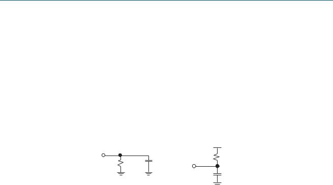
a. The loads presented in Figure 2 are used for tPXZ:
|
tPHZ |
1ΚΩ |
|
1ΚΩ |
5 pF |
||
tPLZ |
|||
|
|||
|
|
||
|
|
5 pF |
Figure 2: Loads used for tPXZ
|
|
|
• |
|
© 2002 QuickLogic Corporation |
www.quicklogic.com |
• |
5 |
|
• |
||||
|
|
|
• |
|
|
|
|
• |
|
|
|
|
• |
|

QL3060 pASIC 3 FPGA Data Sheet Rev D
DC Characteristics
The DC specifications are provided in Table 6 through Table 8.
Table 6: Absolute Maximum Ratings
|
Parameter |
|
|
Value |
|
|
|
|
Parameter |
|
|
|
|
Value |
|
|
|||
|
|
|
|
|
|
|
|
|
|
|
|
|
|
|
|
|
|
||
|
VCC Voltage |
|
|
-0.5 V to 4.6 V |
|
|
|
DC Input Current |
|
|
±20 mA |
|
|
||||||
|
VCCIO Voltage |
|
|
-0.5 V to 7.0 V |
|
|
|
ESD Pad Protection |
|
|
±2000 V |
|
|
||||||
|
Input Voltage |
|
-0.5 V to VCCIO +0.5 V |
|
|
Storage Temperature |
-65°C to +150°C |
||||||||||||
|
Latch-up Immunity |
|
|
±200 mA |
|
|
|
Lead Temperature |
|
|
300°C |
|
|
||||||
|
|
|
|
|
|
|
|
|
|
|
|
|
|
|
|
|
|
||
|
|
|
|
|
Table 7: Operating Range |
|
|
|
|
|
|
|
|||||||
|
|
|
|
|
|
|
|
|
|
|
|
|
|
|
|
||||
|
Symbol |
|
Parameter |
Military |
|
Industrial |
|
Commercial |
Unit |
|
|||||||||
|
|
|
|
|
|
Min |
|
Max |
|
Min |
|
Max |
|
Min |
|
Max |
|
|
|
|
|
|
|
|
|
|
|
|
|
|
|
|
|||||||
|
|
|
|
|
|
|
|
|
|
|
|
|
|
|
|
|
|
|
|
|
VCC |
Supply Voltage |
3.0 |
|
3.6 |
|
3.0 |
|
3.6 |
|
3.0 |
|
3.6 |
V |
|||||
|
VCCIO |
I/O Input Tolerance Voltage |
3.0 |
|
5.5 |
|
3.0 |
|
5.5 |
|
3.0 |
|
5.25 |
V |
|
||||
|
TA |
Ambient Temperature |
-55 |
|
- |
|
-40 |
|
85 |
|
0 |
|
70 |
°C |
|||||
|
|
|
|
|
|
|
|
|
|
|
|
|
|
|
|
|
|
||
|
TC |
Case Temperature |
- |
|
|
125 |
|
- |
|
- |
|
- |
|
- |
°C |
|
|||
|
|
|
|
|
|
|
|
|
|
|
|
|
|
|
|
|
|
|
|
|
|
|
|
|
-0 Speed Grade |
- |
|
|
- |
|
0.43 |
|
1.90 |
|
0.46 |
|
1.85 |
n/a |
|
|
|
|
|
|
|
|
|
|
|
|
|
|
|
|
|
|
|
|
|
|
|
|
|
|
-1 Speed Grade |
0.42 |
|
1.64 |
|
0.43 |
|
1.54 |
|
0.46 |
|
1.50 |
n/a |
|
|
|
|
|
|
|
|
|
|
|
|
|
|
|
|
|
|
|
|
|
|
|
K |
Delay Factor |
-2 Speed Grade |
0.42 |
|
1.37 |
|
0.43 |
|
1.28 |
|
0.46 |
|
1.25 |
n/a |
||||
|
|
|
|
|
|
|
|
|
|
|
|
|
|
|
|
|
|
|
|
|
|
|
|
|
-3 Speed Grade |
|
|
|
|
|
0.43 |
|
0.90 |
|
0.46 |
|
0.88 |
n/a |
|
|
|
|
|
|
|
|
|
|
|
|
|
|
|
|
|
|
|
|
|
|
|
|
|
|
-4 Speed Grade |
|
|
|
|
|
0.43 |
|
0.82 |
|
0.46 |
|
0.80 |
n/a |
|
|
|
|
|
|
|
|
|
|
|
|
|
|
|
|
|
|
|
|
|
•
•
6 • www.quicklogic.com © 2002 QuickLogic Corporation
•
•
•
 Loading...