


QUICK LOGIC QL3004E-1PL68I, QL3004E-1PL68M, QL3004E-1PL84C, QL3004E-1PL84I, QL3004E-1PL84M Datasheet
...
-(.//0 *! . 1 *
02/// # ( 1 *! . 1 #
4,000 Usable PLD Gates with 82 I/Os
300 MHz 16-bit Counters,
400 MHz Datapaths
0.35 m four-layer metal non-volatile CMOS process for smallest die sizes
100% routable with 100% utilization and complete pin-out stability
Variable-grain logic cells provide high performance and 100% utilization
Comprehensive design tools include high quality Verilog/VHDL synthesis
' ( ) *+ ) #'
, ) +
Two array clock/control networks available to the logic cell flip-flop clock, set and reset inputs — each driven by an input-only pin
Two global clock/control networks available to the logic cell; F1, clock, set and reset inputs and the data input, I/O register clock, reset and enable inputs as well as the output enable control — each driven by an inputonly or I/O pin, or any logic cell output or I/O cell feedback
Input + logic cell + output total delays under 6 ns
Data path speeds over 400 MHz
Counter speeds over 300 MHz
! " #
Interfaces with both 3.3 V and 5.0 V devices
PCI compliant with 3.3 V and 5.0 V buses for -1/-2/-3/-4 speed grades
Full JTAG boundary scan
I/O Cells with individually controlled Registered Input Path and Output Enables
$%& ! "
74 bidirectional input/output pins, PCI-compliant for 5.0 V and 3.3 V buses for -1/-2/-3/-4 speed grades
Four High-Drive input-only pins
Four High-Drive/distributed network pins
|
Preliminary

' " )
The QL3004E is a 4,000 usable PLD gate member of the pASIC 3 family of FPGAs. pASIC 3 FPGAs are fabricated on a 0.35 m four-layer metal process using QuickLogic 's patented ViaLink technology to provide a unique combination of high performance, high density, low cost, and extreme ease-of-use.
The QL3004E contains 96 logic cells. With a maximum of 74 I/Os, the QL3004E is available 68-pin PLCC, 84-pin PLCC, and 100-pin TQFP packages.
Software support for the complete pASIC 3 family, including the QL3004E, is available through three basic packages. The turnkey QuickWorks package provides the most complete FPGA software solution from design entry to logic synthesis, to place and route, to simulation. The QuickToolsTM for Workstations package provides a solution for designers who use Cadence , ExemplarTM, Mentor , Synopsys , Synplicity , ViewlogicTM, AldecTM, or other third-party tools for design entry, synthesis, or simulation.
& Preliminary

*
3 4 .5. 32$4 &6°78 4 5//9
To calculate delays, multiply the appropriate K factor from $# : by the numbers provided in $# through $# 6.
* # |
|
7 9 ' |
||||
|
|
|
& |
. |
0 |
% |
|
|
|
|
|
|
|
tPD |
Combinatorial Delay b |
1.4 |
1.7 |
1.9 |
2.2 |
3.2 |
tSU |
Setup Time b |
1.7 |
1.7 |
1.7 |
1.7 |
1.7 |
tH |
Hold Time |
0.0 |
0.0 |
0.0 |
0.0 |
0.0 |
tCLK |
Clock to Q Delay |
0.7 |
1.0 |
1.2 |
1.5 |
2.5 |
tCWHI |
Clock High Time |
1.2 |
1.2 |
1.2 |
1.2 |
1.2 |
tCWLO |
Clock Low Time |
1.2 |
1.2 |
1.2 |
1.2 |
1.2 |
tSET |
Set Delay |
1.0 |
1.3 |
1.5 |
1.8 |
2.8 |
tRESET |
Reset Delay |
0.8 |
1.1 |
1.3 |
1.6 |
2.6 |
tSW |
Set Width |
1.9 |
1.9 |
1.9 |
1.9 |
1.9 |
tRW |
Reset Width |
1.8 |
1.8 |
1.8 |
1.8 |
1.8 |
! " # # !$" %&°' ( ) * +* * *
$# :
( ( ( ( ( (
$, #- ( (
|
Preliminary |
|
|
|
. |
||
|
|
|
|
|
|
|
||
|

% , ./ 0
* # |
|
7 9 ' |
||||||
|
|
|
& |
. |
0 |
% |
& |
&0 |
|
|
|
|
|
|
|
|
|
tIN |
High Drive Input Delay |
1.5 |
1.6 |
1.8 |
1.9 |
2.4 |
2.9 |
4.4 |
tINI |
High Drive Input, Inverting Delay |
1.6 |
1.7 |
1.9 |
2.0 |
2.5 |
3.0 |
4.5 |
tISU |
Input Register Set-Up Time |
3.1 |
3.1 |
3.1 |
3.1 |
3.1 |
3.1 |
3.1 |
tIH |
Input Register Hold Time |
0.0 |
0.0 |
0.0 |
0.0 |
0.0 |
0.0 |
0.0 |
tlCLK |
Input Register Clock To Q |
0.7 |
0.8 |
1.0 |
1.1 |
1.6 |
2.1 |
3.6 |
tlRST |
Input Register Reset Delay |
0.6 |
0.7 |
0.9 |
1.0 |
1.5 |
2.0 |
3.5 |
tlESU |
Input Register clock Enable Set-Up Time |
2.3 |
2.3 |
2.3 |
2.3 |
2.3 |
2.3 |
2.3 |
tlEH |
Input Register Clock Enable Hold Time |
0.0 |
0.0 |
0.0 |
0.0 |
0.0 |
0.0 |
0.0 |
! " # # !$" %&°' ( ) * +* * *
$# :
#
* # |
|
7 9 ( |
' |
|||||
|
|
|
& |
. |
0 |
% |
/ |
|
|
|
|
|
|
|
|
|
|
tACK |
Array Clock Delay |
1.2 |
1.2 |
1.3 |
1.3 |
1.5 |
1.6 |
1.7 |
tGCKP |
Global Clock Pin Delay |
0.7 |
0.7 |
0.7 |
0.7 |
0.7 |
0.7 |
0.7 |
tGCKB |
Global Clock Buffer Delay |
0.8 |
0.8 |
0.9 |
0.9 |
1.1 |
1.2 |
1.3 |
( %1 ( (
%2 ( * ( ( (
( ( ( ( (
( 3 (
0 Preliminary
1 , ./ ,0/
* # |
|
7 9 ' |
|||||
|
|
|
& |
. |
0 |
% |
/ |
|
|
|
|
|
|
|
|
tI/O |
Input Delay (bidirectional pad) |
1.3 |
1.6 |
1.8 |
2.1 |
3.1 |
3.6 |
tISU |
Input Register Set-Up Time |
3.1 |
3.1 |
3.1 |
3.1 |
3.1 |
3.1 |
tIH |
Input Register Hold Time |
0.0 |
0.0 |
0.0 |
0.0 |
0.0 |
0.0 |
tlOCLK |
Input Register Clock To Q |
0.7 |
1.0 |
1.2 |
1.5 |
2.5 |
3.0 |
tlORST |
Input Register Reset Delay |
0.6 |
0.9 |
1.1 |
1.4 |
2.4 |
2.9 |
tlESU |
Input Register clock Enable Set-Up Time |
2.3 |
2.3 |
2.3 |
2.3 |
2.3 |
2.3 |
tlEH |
Input Register Clock Enable Hold Time |
0.0 |
0.0 |
0.0 |
0.0 |
0.0 |
0.0 |
! " # # ! |
||||||||
$" %&°' ( ) * +* * * |
||||||||
$# : |
|
|
|
|
|
|
|
|
|
& / ./ ,0/ |
|
|
|
|
|
||
|
|
|
|
|
|
|
|
|
* # |
|
7 9 "' ' ( |
|
|||||
|
7 9 |
|
||||||
|
|
|
|
|||||
|
|
./ |
|
:6 |
|
// |
|
6/ |
|
|
6/ |
|
|
||||
|
|
|
|
|
|
|
|
|
tOUTLH |
Output Delay Low to High |
2.1 |
2.5 |
3.1 |
|
3.6 |
|
4.7 |
tOUTHL |
Output Delay High to Low |
2.2 |
2.6 |
3.2 |
|
3.7 |
|
4.8 |
tPZH |
Output Delay Tri-state to High |
1.2 |
1.7 |
2.2 |
|
2.8 |
|
3.9 |
tPZL |
Output Delay Tri-state to Low |
1.6 |
2.0 |
2.6 |
|
3.1 |
|
4.2 |
tPHZ |
Output Delay High to Tri-State a |
2.0 |
- |
- |
|
- |
|
- |
tPLZ |
Output Delay Low to Tri-State |
1.2 |
- |
- |
|
- |
|
- |
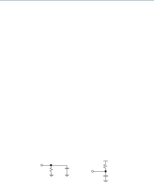
(' & 45
|
tPHZ |
1ΚΩ |
|
1ΚΩ |
5 pF |
||
tPLZ |
|||
|
|||
|
|
||
|
|
5 pF |
|
Preliminary |
|
|
|
6 |
||
|
|
|
|
|
|
|
||
|

The DC specifications are provided in $# ; through $# %.
6$' 7 8
|
|
|
3 ' |
|
|
|
|
|
|
3 ' |
|
|
||||||
|
|
|
|
|
|
|
|
|
|
|
|
|
|
|
|
|||
|
|
VCC Voltage |
-0.5 V to 4.6 V |
|
DC Input Current |
|
|
±20 mA |
||||||||||
|
VCCIO Voltage |
-0.5 V to 7.0 V |
ESD Pad Protection |
|
|
±2000 V |
||||||||||||
|
Input Voltage |
-0.5 V to VCCIO +0.5 V |
Storage Temperature |
|
|
-65°C to +150°C |
||||||||||||
|
Latch-up Immunity |
±200 mA |
|
|
Lead Temperature |
|
|
300°C |
||||||||||
|
|
|
|
|
|
|
|
|
|
|
|
|
|
|
|
|
||
|
|
|
|
3 / 8 |
|
|
|
|
|
|
|
|
|
|||||
|
|
|
|
|
|
|
|
|
|
|
|
|
|
|
|
|
|
|
* # |
|
|
|
< |
|
! |
' |
|
|
|
|
|
||||||
|
|
|
|
|
|
|
|
|
|
|
|
|
|
|
|
|
|
|
|
|
|
|
|
|
< |
< = |
|
< |
|
< = |
|
< |
< = |
|
|
|
|
|
|
|
|
|
|
|
|
|
|
|
|
|
|
|
|
|
|
|
|
VCC |
|
Supply Voltage |
|
|
3.0 |
3.6 |
|
3.0 |
|
3.6 |
|
3.0 |
3.6 |
|
V |
||
|
VCCIO |
|
I/O Input Tolerance Voltage |
|
3.0 |
5.5 |
|
3.0 |
|
5.5 |
|
3.0 |
5.25 |
|
V |
|
||
|
TA |
|
Ambient Temperature |
|
-55 |
- |
|
-40 |
|
85 |
|
0 |
|
70 |
|
°C |
||
|
|
|
|
|
|
|
|
|
|
|
|
|
|
|
|
|
|
|
|
TC |
|
Case Temperature |
|
- |
125 |
|
- |
|
- |
|
- |
|
- |
|
°C |
|
|
|
|
|
|
|
|
|
|
|
|
|
|
|
|
|
|
|
|
|
|
|
|
|
-0 Speed Grade |
|
- |
- |
|
0.43 |
|
1.90 |
|
0.46 |
1.85 |
|
n/a |
||
|
|
|
|
|
|
|
|
|
|
|
|
|
|
|
|
|
|
|
|
|
|
|
-1 Speed Grade |
|
0.42 |
1.64 |
|
0.43 |
|
1.54 |
|
0.46 |
1.50 |
|
n/a |
|
|
|
|
|
|
|
|
|
|
|
|
|
|
|
|
|
|
|
|
|
|
K |
|
Delay Factor |
-2 Speed Grade |
|
0.42 |
1.37 |
|
0.43 |
|
1.28 |
|
0.46 |
1.25 |
|
n/a |
||
|
|
|
|
|
|
|
|
|
|
|
|
|
|
|
|
|
|
|
|
|
|
|
-3 Speed Grade |
|
|
|
|
0.43 |
|
0.90 |
|
0.46 |
0.88 |
|
n/a |
|
|
|
|
|
|
|
|
|
|
|
|
|
|
|
|
|
|
|
|
|
|
|
|
|
-4 Speed Grade |
|
|
|
|
0.43 |
|
0.82 |
|
0.46 |
0.80 |
|
n/a |
||
|
|
|
|
|
|
|
|
|
|
|
|
|
|
|
|
|
|
|
; Preliminary
 Loading...