

Philips NE591N, NE590N Datasheet

Philips Semiconductors Linear Products Product specification
NE590/591Addressable peripheral drivers
518
August 31, 1994 853-0951 13721
DESCRIPTION
The NE590/591 addressable peripheral drivers are high current
latched drivers, similar in function to the 9334 address decoder. The
device has eight Darlington power outputs, each capable of 250mA
load current. The outputs are turned on or off by respectively loading
a logic high or logic low into the device data input. The required
output is defined by a 3-bit address. The device must be enabled by
a CE
input line. A common clear input, CLR, turns all outputs off
when a logic low is applied.
The NE590 has eight open-collector Darlington outputs which sink
current to ground. The device is packaged in a 16-pin plastic or
Cerdip package.
The NE591 has eight open-emitter Darlington outputs which source
current to an external load from a common collector line, V
S
. This
V
S
line need not necessarily be the same as the 5V VCC supply. The
device is packaged in an 18-pin plastic or Cerdip package.
FEATURES
•8 high current outputs
•Low-loading bus compatible inputs
•Power-on clear ensures safe operation
•NE590 will operate in addressable or demultiplex mode
•Allows random (addressed) data entry
•Easily expandable
•NE590 is pin compatible with 54/74LS259
APPLICATIONS
•Relay driver
•Indicator lamp driver
•Triac trigger
•LED display digit driver
•Stepper motor driver
PIN CONFIGURATIONS
N Package
NE590
N Package
NE591
1
2
3
4
5
6
7
8
9
10
11
12
13
14
16
15
TOP VIEW
1
2
3
4
5
6
7
8
11
12
13
14
15
16
18
17
9
10
A
0
A
1
A
2
Q
0
Q
1
Q
2
Q
3
GND
A
0
A
1
A
2
Q
0
Q
1
Q
2
Q
3
GND
CS
V
CC
CLR
CE
D
Q
7
Q
6
Q
5
Q
4
V
CC
CLR
CE
D
Q
7
Q
6
Q
5
Q
4
V
S
TOP VIEW
ORDERING INFORMATION
DESCRIPTION TEMPERATURE RANGE ORDER CODE DWG #
16-Pin Plastic Dual In-Line Package (DIP) 0 to +70°C NE590N 0406C
18-Pin Plastic Dual In-Line Package (DIP) 0 to +70°C NE591N 0406C
Philips Semiconductors Linear Products Product specification
NE590/591Addressable peripheral drivers
August 31, 1994
519
PIN DESIGNATION
590
PIN NO.
591
PIN NO.
SYMBOL NAME & FUNCTION
1-3 2-4 A0-A
2
A 3-bit binary address on these pins defines which of the 8 output latches is to receive the data.
4-7,
9-12
5-8,
11-14
Q0-Q
7
The 8 device outputs. The NE590 has open-collector Darlington outputs. The NE591 has open emitter-follower outputs.
13 15 D The data input. When the chip is enabled, this data bit is transferred to the defined output such that:
“1” turns output switch “ON”
“0” turns output switch “OFF”
Thus in logic terms, the NE590 inverts data to the relevant output. The NE591 retains true data at the
output.
14 16 CE The chip enable. When this input is low, the output latches will accept data. When CE goes high, all
outputs will retain their existing state regardless of address or data input conditions.
15 17 CLR The clear input. When CLR goes low all output switches are turned “OFF”. On the NE590, a high
data input will override the clear function on the addressed latch. On the NE591, CLR
low will over-
ride any other condition.
- 1 CS The chip select input provides for an additional level of address decoding.
- 10 V
S
The VS line provides the power to all 8 output devices. It is connected to the collectors of all 8 output
transistors. This pin may be connected to the V
CC
or another supply.
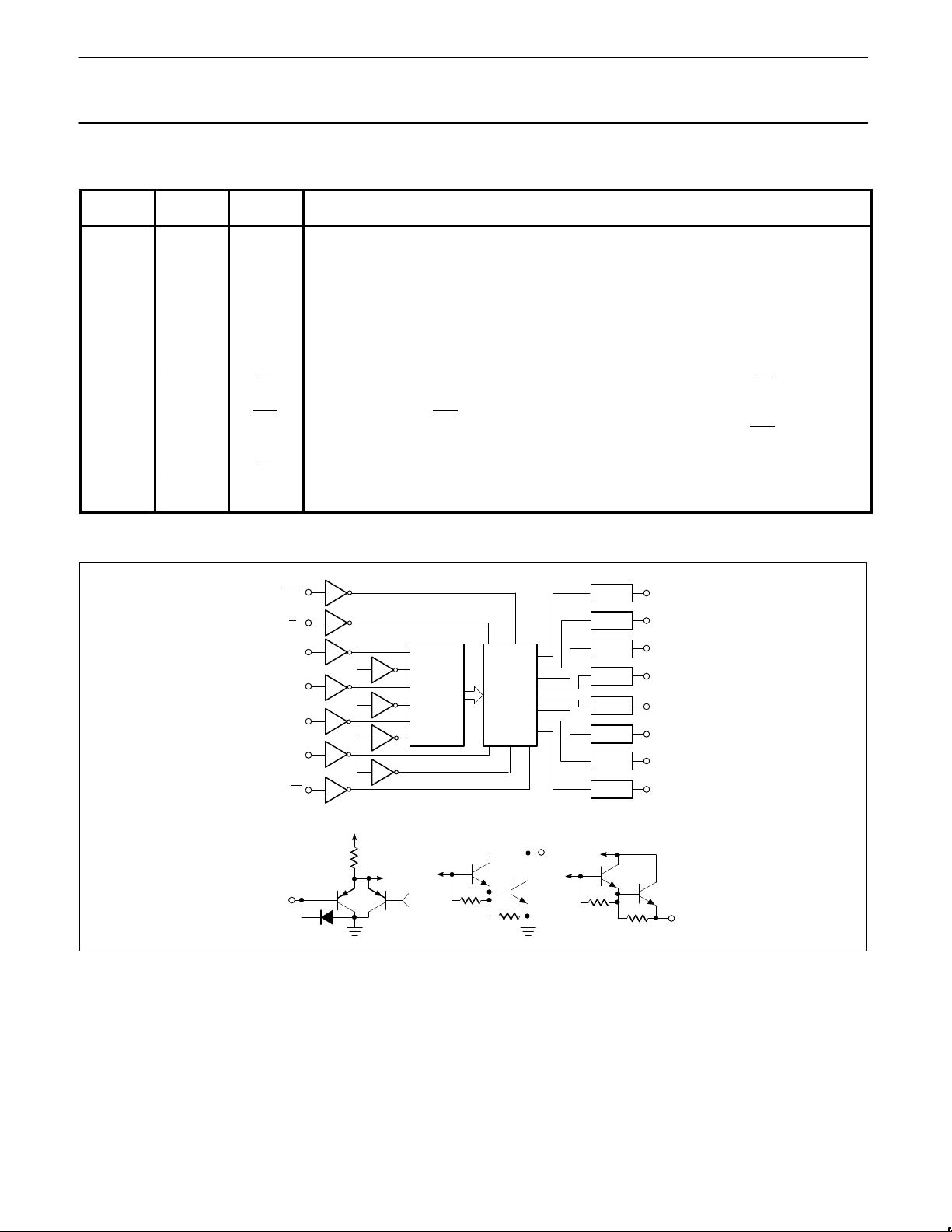
BLOCK DIAGRAM
LATCH
LATCH
LATCH
LATCH
LATCH
LATCH
LATCH
LATCH
CLR
CE
A
0
A
1
A
2
D
1–OF–8
DECODER
COMTROL
GATE
V
CC
NE590
Q
0
Q
1
Q
2
Q
3
Q
4
Q
5
Q
6
Q
7
cs
(NE51 ONLY)
INPUT STAGE
NE591
OUTPUT STAGE
Philips Semiconductors Linear Products Product specification
NE590/591Addressable peripheral drivers
August 31, 1994
520
TRUTH TABLE (NE590)
INPUTS OUTPUTS MODE
CLRCED A0A1A2Q0Q1Q2Q3Q4Q5Q6Q
7
L H X X X X H H H H H H H H Clear
L L L L L L H H H H H H H H
L L H L L L L H H H H H H H
L L L H L L H H H H H H H H Demultiplex
L L H H L L H L H H H H H H
L L L H H H H H H H H H H H
L L H H H H H H H H H H H L
H H X X X X Q
N-1
Memory
H L L L L L H Q
N-1
H L H L L L L Q
N-1
H L L H L L Q
N-1
H Q
N-1
Addressable Latch
H L H H L L Q
N-1
L Q
N-1
H L L H H H Q
N-1
H
H L H H H H Q
N-1
L
NOTES:
X=Don’t care condition
Q
N-1
=Previous output state
L=Low voltage level/“OFF” output state
H=High voltage level/“ON” output state
TRUTH TABLE (NE591)
INPUTS OUTPUTS MODE
CLRCECSD A0A1A2Q0Q1Q2Q3Q4Q5Q6Q
7
L X X X X X X L L L L L L L L Clear
H H H X X X X Q
N-1
H H L X X X X Q
N-1
Memory
H L H X X X X Q
N-1
H L L L L L L L Q
N-1
H L L H L L L H Q
N-1
H L L L H L L Q
N-1
L Q
N-1
Addressable Latch
H L L H H L L Q
N-1
H Q
N-1
H L L L H H H Q
N-1
L
H L L H H H H Q
N-1
H
NOTES:
X=Don’t care condition
Q
N-1
=Previous output state
L=Low voltage level/“OFF” output state
H=High voltage level/“ON” output state
 Loading...