

Philips ne587 DATASHEETS

Philips Semiconductors Linear Products Product specification
NE587LED decoder/driver
530
August 31, 1994 853-1095 13721
DESCRIPTION
The NE587 is a latch/decoder/driver for 7-segment common anode
LED displays. The NE587 has a programmable current output up to
50mA which is essentially independent of output voltage, power
supply voltage, and temperature. The data (BCD) inputs and LE
(latch enable) input are low-loading so that they are compatible with
any data bus system. The 7-segment decoding is implemented with
a ROM so that alternative fonts can be made available.
FEATURES
•Latched BCD inputs
•Low loading bus-compatible inputs
•Ripple-blanking on leading- and/or trailing-edge zeros
APPLICATIONS
•Digital panel motors
•Measuring instruments
•Test equipment
•Digital clocks
•Digital bus monitoring
PIN CONFIGURATIONS
1
2
3
4
5
6
7
8
9
10
11
12
18
17
16
15
14
13
1
2
3
4
5
6
7
8
9
10
11
12
13
14
20
19
18
17
16
15
D
1
D
2
LE
BI/RBO
DIG GND
RBI
I
P
D
3
D
0
V
CC
f
g
a
POWER GND
b
e
c
d
D
1
D
2
LE
BI/RBO
DIG GND
RBI
I
P
D
3
D
0
V
CC
f
g
a
POWER GND
b
e
NC
d
NC
c
N Package
D1 Package
NOTE:
1. SOL and non-standard pinout.
ORDERING INFORMATION
DESCRIPTION TEMPERATURE RANGE ORDER CODE DWG #
20-Pin Plastic Small Outline Large (SOL) Package 0 to +70°C NE587D
1
0172D
18-Pin Plastic Dual In-Line Package (DIP) 0 to +70°C NE587N 0407A
NOTES:
1. SOL and non-standard pinout
ABSOLUTE MAXIMUM RATINGS
TA=25°C unless otherwise specified.
SYMBOL
PARAMETER RATING UNIT
V
CC
Supply voltage -0.5 to +7 V
V
IN
Input voltage
(D
0-D3
, LE, RBI)
-0.5 to +15 V
V
OUT
Output voltage
(a-g, RBO)
-0.5 to +7 V
P
D
Power dissipation (25°C)
1
1000 mW
T
A
Ambient temperature range 0 to 70 °C
T
J
Junction temperature 150 °C
T
STG
Storage temperature range -65 to +150 °C
T
SOLD
Soldering temperature (10sec max) 300 °C
NOTES:
1. Derate power dissipation as indicated
N package—95°C/W above 55°C
Philips Semiconductors Linear Products Product specification
NE587LED decoder/driver
August 31, 1994
531
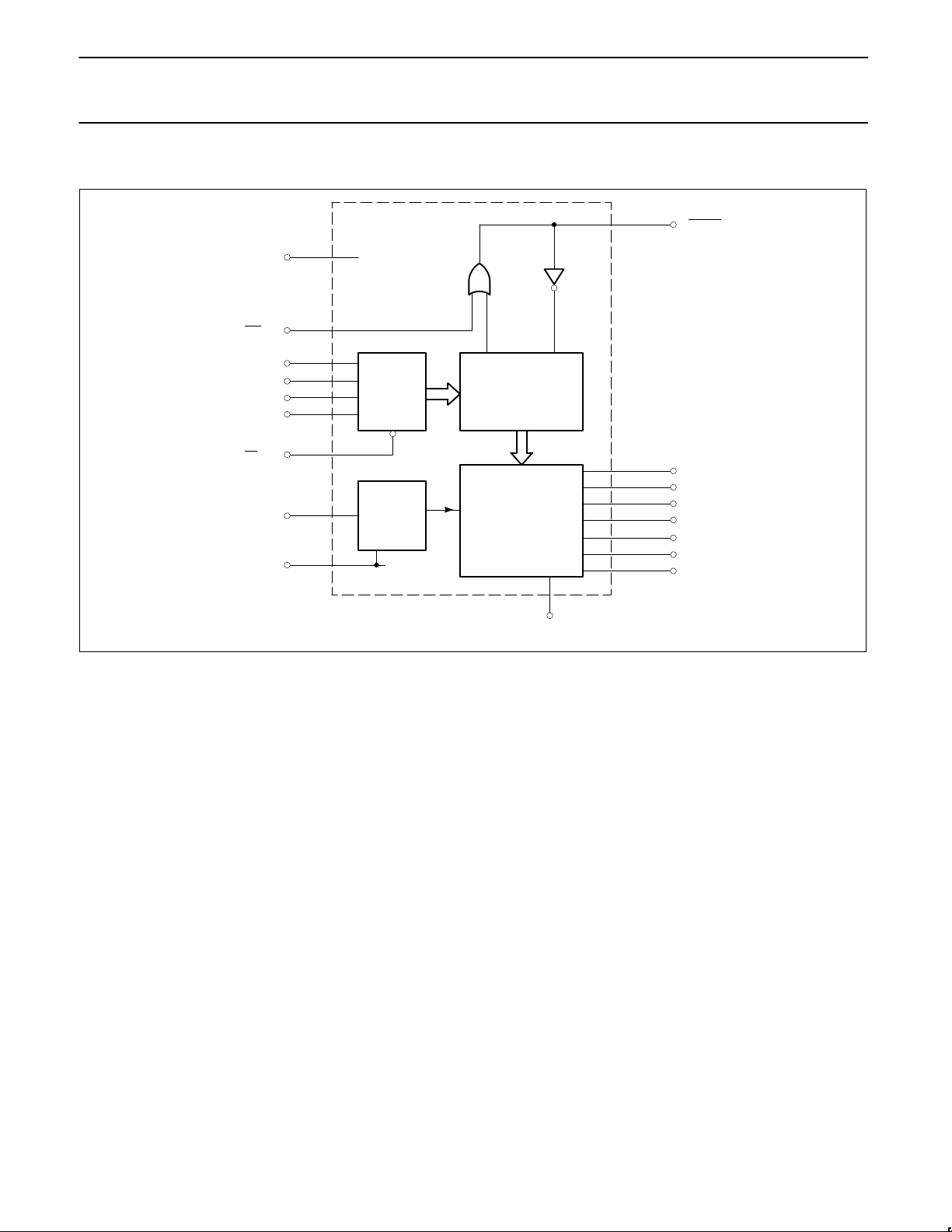
BLOCK DIAGRAM
..
..
D
1
D
2
LE
BI/RBO
GND
RBI
I
P
D
3
D
0
V
CC
f
g
a
POWER GND (10)
b
e
d
c
(18)
(5)
(7)
(1)
(2)
(6)
(3)
(8)
(9)
(4)
(15)
(14)
(13)
(12)
(11)
(17)
(16)
DATA
LATCHES
BCD TO
7-SEGMENT
DECODER
SEGMENT
CURRENT
DRIVER
BANDGAP
REFERENCE
Philips Semiconductors Linear Products Product specification
NE587LED decoder/driver
August 31, 1994
532
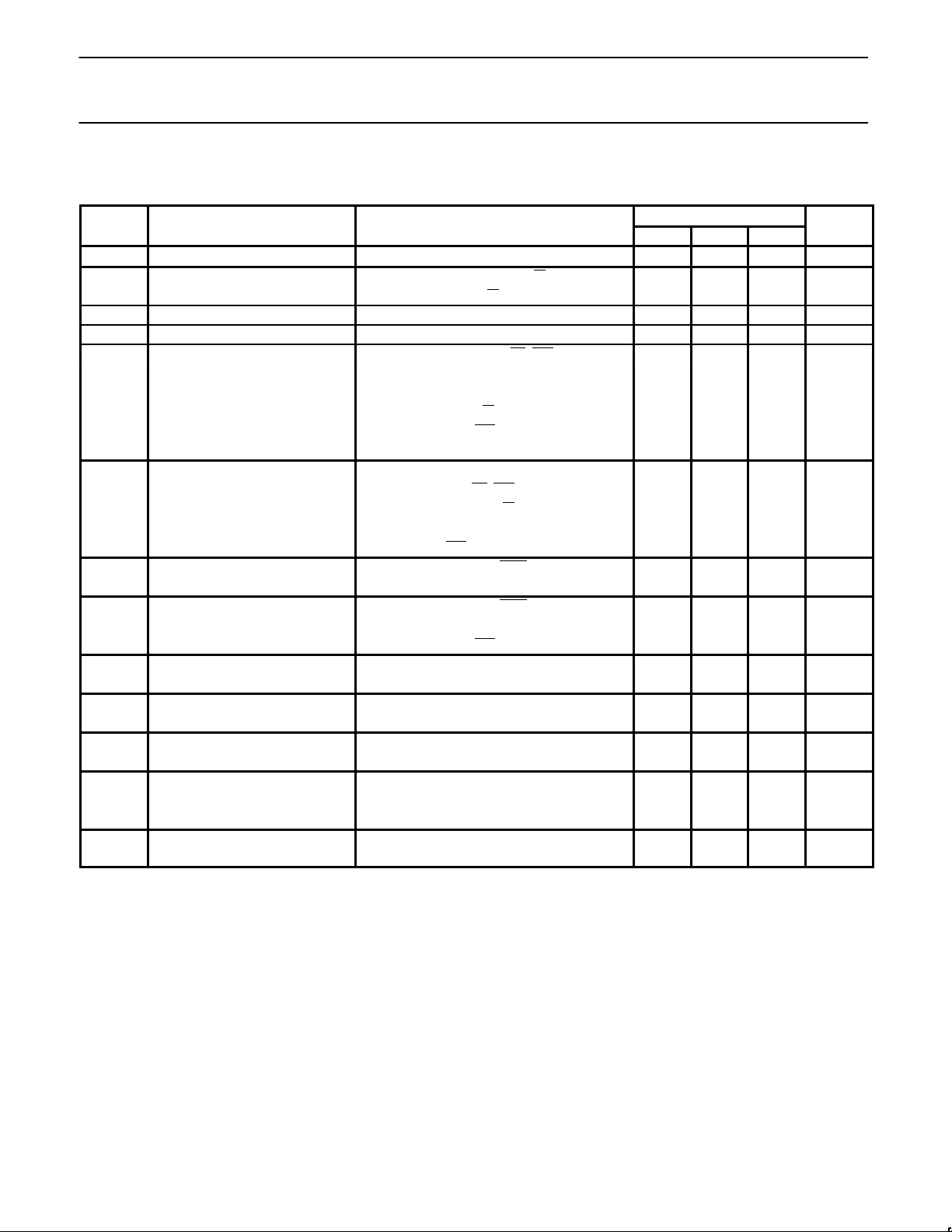
DC ELECTRICAL CHARACTERISTICS
VCC=4.75 to 5.25V, 0°C < T
A
< 70°C. Typical values are at VCC=5V, TA=25°C, RP=1kΩ (±1%), unless otherwise specified.
LIMITS
SYMBOL
PARAMETER
TEST CONDITIONS
Min Typ Max
UNIT
V
CC
Operating supply voltage 4.75 5.00 5.25 V
V
IH
Input high voltage All inputs except BI 2.0 15 V
BI 2.0 5.5
V
IL
Input low voltage 0.8 V
V
IC
Input clamp voltage IIN=-12mA, TA=25°C -1.5 V
Inputs D0-D3, LE, RBI µA
VIN=2.4V 1.0 10
I
IH
Input high current VIN=15V 15 15
Input BI (Pin 4) 10 100 µA
RBI=H
VIN=VCC=5.25V
VIN=0.4V, Inputs D0-D
3
-5
I
IL
Input low current LE, RBI -200 µA
Input BI
VCC=5.25V -0.7 mA
RBI=H, VIN=0.4V
V
OL
Output low voltage Output RBO 0.2 0.5 V
I
OUT
=3.0mA
Output RBO
V
OH
Output high voltage I
OUT
=-50µA 3.5 4.5 V
RBI=H
I
OUT
Output segment Outputs “a” through “g” 20 25 30 mA
“ON” current V
OUT
=2.0V
∆I
OUT
Output current ratio With reference to “b” segment 0.90 1.00 1.10
(all outputs ON) V
OUT
=2.0V
Output segment Outputs “a” through “g”
I
OFF
“OFF” current V
OUT
=5.0V 20 250 µA
VCC=5.25V
I
CCO
Supply current All outputs “ON” 33 55 mA
V
OUT
>1V
VCC=5.25V
I
CCI
Supply current All outputs blanked 50 70 mA
NOTES:
NE587 Programming:
The NE587 output current can be programmed, provided a program resistor, R
P
, be connected between IP (Pin 8) and Ground (Pin 9). The
voltage at I
P
(Pin 8) is constant (≈1.3V). Thus, a current through RP is IP ≈ 1.3V/RP, as shown in Figure 5. IO/IP is 20 in the 15 to 50mA output
current range.
 Loading...