

Page 1
ORDER NO. MD0510379C1 A6
Speaker System
MODEL UNIT
SC-TM44 SA-TM44 Stereo
SB-TM44
Specifications
POTENCIA DE SALIDA (AMPLIFICADOR)
SC-TM44 Colour (S)... Silver Type
SB-TM44 Front Speaker
SA-TM44
SB-TM44
SC-TM44 Frontal (Bajo) 105 W RCM por canal (3Ω) 1kHz, 10% DAT
Amplificador SA-TM 44
Potencia de salida 4600 W (P.M.P.O)
Consumo de potencia 125 W
Alimentaciòn 127 V ca ±10% 60 Hz
Sencibilidad music port: 100 mV
Rango de sintonìa AM:
Rango de sintonìa FM:
Dimensiones
: 6.6 kg aprox
Peso
Notes: Specifications ar e subject to chan ge without notice. Mass and dimens ions are approximate.Total harmonic distortion is me asured by the digital spect rum analyzer.
© 2004 Matsushita Electric Industrial Co. Ltd.. All rights reserved. Unauthorized copying and distribution is a violation of law.
(b x h x l) 250 mm x 330 mm x 343mm
520-1710MHz (paso de 0,2 MHz)
87.9-107.9 MHz (paso de 0,2 MHz
87.5-108.0 MHz (paso de 0,1 MHz
(Alto)105 W RCM por canal (3Ω) 10kHz, 10% DAT
Bafles SB-TM 44
FRONTAL
Bocina Super Tweeter piezo type
ina Tweeter 6 cm
Boc
Bocina Woofer 16
IMPEDANCI
Fronta
o 3 Ω
Alt
jo 3 Ω
Ba
Dimensiones
Peso: 3.4 kg aprox
A
l - - - - - -
(b x h x l) 247 mm x 330 mm x 221mm
cm
Page 2
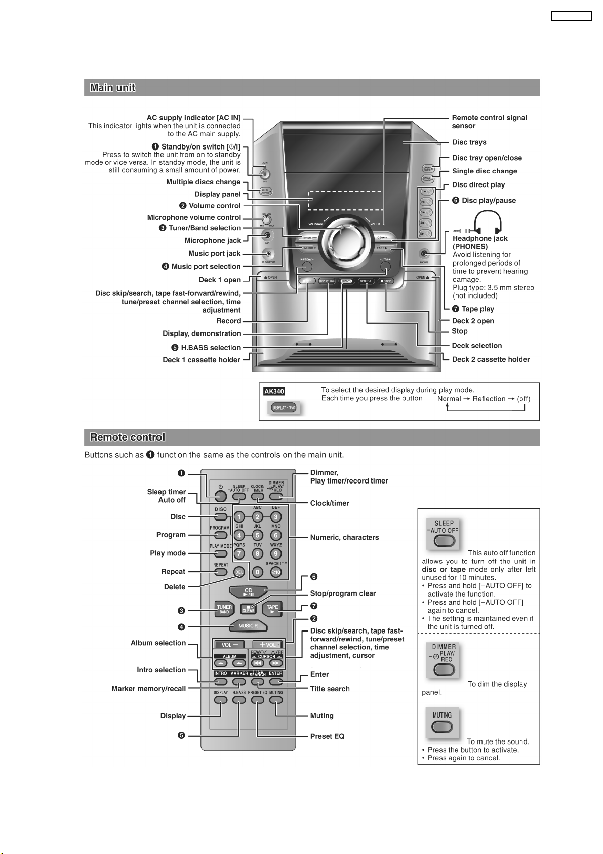
1 Safety Precautions
1.1. General Guidelines
1. When servicing, observe the original lead dress. If a short circuit is found, replace all parts which have been overheated or
damaged by the short circuit.
2. After servicing, ensure that all the protective devices such as insulation barriers and insulation papers shields are properly
installed.
3. After servicing, check for leakage current checks to prevent from being exposed to shock hazards.
1.1.1. Leakage Current Cold Check
1. Unplug the AC cord and connect a jumper between the two prongs on the plug.
2. Using an ohmmeter measure the resistance value, between the jumpered AC plug and each exposed metallic cabinet part on
the equipment such as screwheads, connectors, control shafts, etc. When the exposed metallic part has a return path to the
chassis, the reading should be between 1MΩ and 5.2MΩ.
When the exposed metal does not have a return path to the chassis, the reading must be
.
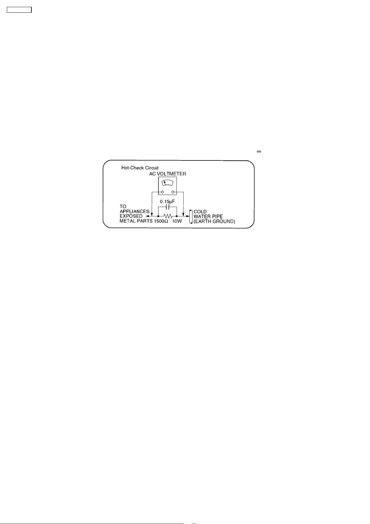
Fig. 1
1.1.2. Leakage Current Hot Check (See Figure 1)
1. Plug the AC cord directly into the AC outlet. Do not use an isolation transfo rmer for this check.
2. Connect a 1.5kΩ, 10 watts resistor, in parallel with a 0.15µF capacitor, between each expose d metallic part on the set and a
good earth ground such as a water pipe, as shown in Figure 1.
3. Use an AC voltmeter, with 1000 ohms/volt or more sensitivity, to measure the potential across the resistor.
4. Check each exposed metallic part, and measure the voltage at each point.
5. Reverse the AC plug in the AC outlet and repeat each of the above measurements.
6. The potential at any point should not exceed 0.75 volts RMS. A leakage current tester (Simpson Model 229 or equivalent) may
be used to make the hot checks, leakage current must not exceed 1/2 milliamp. Should the measurement is out of the limits
specified, there is a possibility of a shock hazard, and the equipment should be repaired and rechecked before it is returned to
the customer.
1.2. Before repair and adjustment
Disconnect AC power, discharge Power Capacitors C5101, C5104, C5171, C5172, C5920, C5940 and C5950 through a 10Ω,5W
resistor to ground.
DO NOT SHORT-CIRCUIT DIRECTLY (with a screwdriver blade, for instance), as this may destroy solid state devices.
After repairs are completed, restore power gradually using a variac, to avoid overcurrent.
Current consumption at AC 120V, 60 Hz in NO SIGNAL mode (volume min at CD mode) should be ~ 300mA.
1.3. Protection Circuitry
The protection circuitry may have operated if either of the following conditions are noticed:
· No sound is heard when the power is turned on.
· Sound stops during a performance.
The function of this circuitry is to prevent circuitry damage if, for example, the positive and negative speaker connec tion wires are
“shorted”, or if speaker systems with an impedance less than the indicated rated impedance of the amplifier are used.
If this occurs, follow the procedure outlines below:
1. Turn off the power.
2. Determine the cause of the problem and correct it.
2
Page 3
3. Turn on the power once again after one minute.
Note :
When the protection circuitry functions, the unit will not operate unless the power is first turned off and then on again.
2 Prevention of Electro Static Discharge (ESD) to
Electrostatically Sensitive (ES) Devices
Some semiconductor (solid state) devices can be damaged easily by electricity. Such components commonly are called
Electrostatically Sensitive (ES) Devices. Examples of typical ES devices are integrated circuits and some field-effect transistors and
semiconductor “chip” components. The following techniques should be used to help reduce the incidence of component damage
caused by electro static discharge (ESD).
1. Immediately before handling any semiconductor component or semiconductor-equiped assembly, drain off any ESD on your
body by touching a known earth ground. Alternatively, obtain and wear a commercially available discharging ESD wrist strap,
which should be removed for potential shock reasons prior to applying power to the unit under test.
2. After removing an electrical assembly equiped with ES devices, place the assembly on a conductive surface such as aluminium
foil, to prevent electrostatic charge build up or exposure of the assembly.
3. Use only a grounded-tip soldering iron to solder or unsolder ES devices.
4. Use only an anti-static solder remover device. Some solder removal devices not classified as “anti-static (ESD protected)” can
generate electrical charge to damage ES devices.
5. Do not use freon-propelled chemicals. These can generate electrical charges sufficient to damage ES devices.
6. Do not remove a replacement ES device from its protective package until immediately before you are ready to install it. (Most
replacement ES devices are packaged with leads electrically shorted together by conductive foam, aluminium foil or
comparable conductive material).
7. Immediately before removing the protective material from the leads of a replacement ES device, touch the protective material
to the chassis or circuit assembly into which the device will be installed.
Caution
Be sure no power is applied to the chassis or circuit, and observe all other safety precautions.
8. Minimize body motions when handling unpackaged replacement ES devices. (Otherwise harmless motion such as the brushing
together of your clothes fabric or the lifting of your foot from a carpeted floor can generate static electricity (ESD) sufficient to
damage an ES device).
3
Page 4
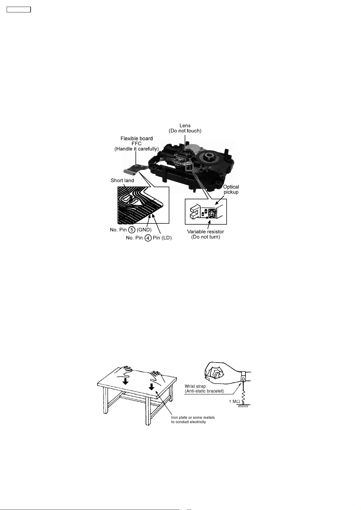
3 Handling Precautions For Traverse Deck
The laser diode in the traverse deck (optical pickup) may break down due to potential difference caused by the static electricity of
clothes or our human body.
So, be careful of electrostatic breakdown during repair of the traverse deck (optical pickup).
· Way of handling the traverse deck (optical pickup)
1. Do not subject the traverse deck (optical pickup) to static electricity as it is extremely sensitive to electrical shock.
2. To prevent the breakdown of the laser diode, an antistatic shorting pin is inserted into the flexible board (FFC board).
3. Do not to apply excessive stress to the flexible board (FFC board). When removing or connecting the short pin, finish the job
in as short time as possible.
4. Do not turn the variable resistor for laser power adjustment. (It is pre-adjusted during production time)
Grounding for electrostatic breakdown prevention
1. Human body grounding
Use the anti-static wrist strap to discharge the static electricity from your body.
2. Work table grounding
Put a conductive material (sheet) or steel sheet on the area where the traverse deck (optical pickup) is place, and ground the
sheet.
Caution :
The static electricity of your clothes will not be grounded through the wrist strap. So, take care not to let your clothes touch the
traverse deck (optical pickup).
Caution when replacing the Traverse Deck
The traverse deck has a short point shorted with solder to protect the laser diode against electrostatics breakdown. Be sure to
remove the solder from the short point before making connections.
4
Page 5
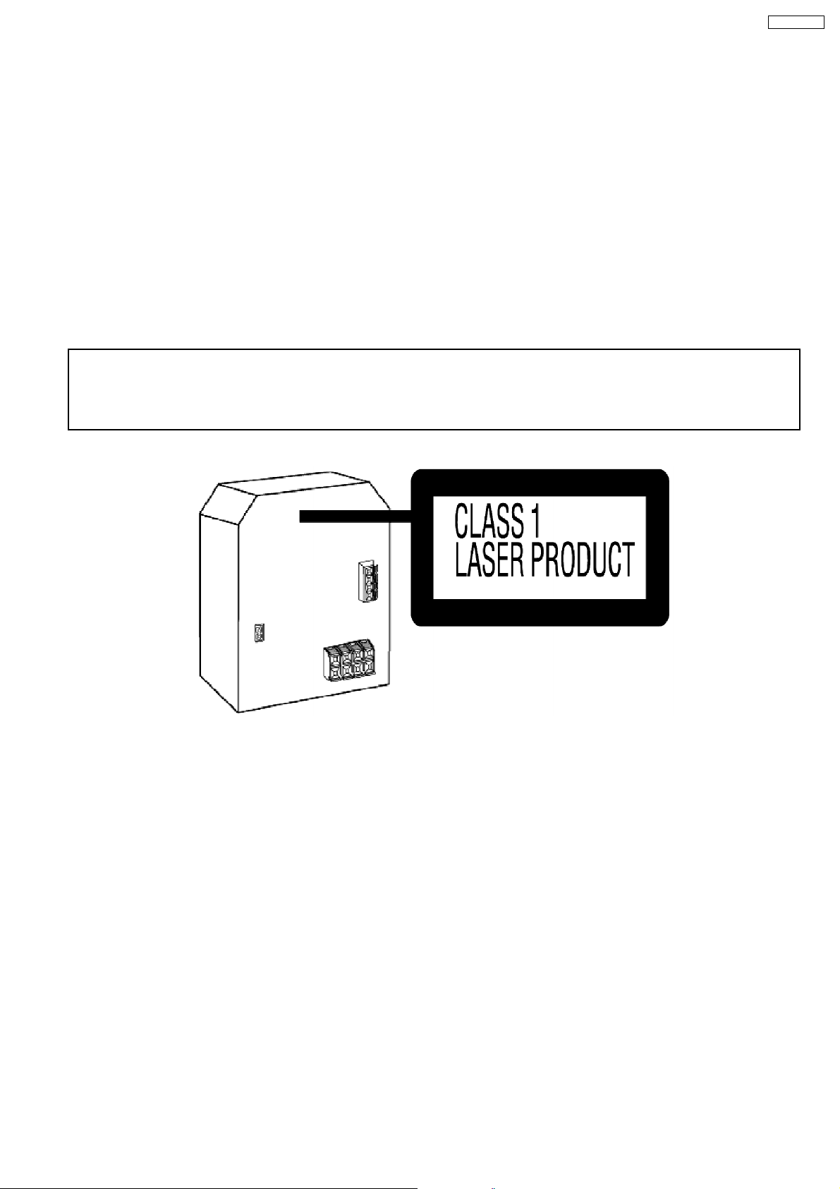
4 Precaution of laser diode
CAUTION:
This unit utilizes a class 1 laser diode in the optical pickup unit .
Invisible laser radiation is emitted from the optical pickup lens.
Wavelength: 780nm
When the unit is turned on:
1. Do not look directly into the optical pickup lens.
2. Do not use optical instruments to look at the optical pickup lens.
3. Do not adjust the preset variable resistor on the optical pickup lens.
4. Do not disassemble the optical optical pickup unit.
5. If the optical pickup is replaced, use the manufacturer’s specified replacement pickup only.
6. Use of control or adjustments or performance of procedures other than those specified herein may result in hazardous radiation
exposure.
CAUTION!
THIS PRODUCT UTILIZES A LASER.
USE OF CONTROLS OR ADJUSTMENTS OR PERFORMANCE OF PROCEDURES OTHER THAN THOSE SPECIFIED HEREIN MAY RESULT
IN HAZARDOUS RADIATION EXPOSURE.
n Use of caution label
5
Page 6

5 Handling the Lead-free Solder
5.1. About lead free solder (PbF)
Distinction of PbF P.C.B.:
P.C.B.s (manufactured) using lead free solder will have a PbF stamp on the P.C.B.
Caution:
· Pb free solder has a higher melting point than standard solder; Typically the melting point is 50 - 70°F (30 - 40°C) higher. Please
use a high temperature soldering iron. In case of soldering iron with temperature control, please set it to 700 ± 20°F (370 ±
10°C).
· Pb free solder will tend to splash when heated too high (about 1100°F/600°C).
· W hen soldering or unsoldering, please completely remove all of the solder on the pins or solder area, and be sure to heat the
soldering points with the Pb free solder until it melts enough.
6
Page 7
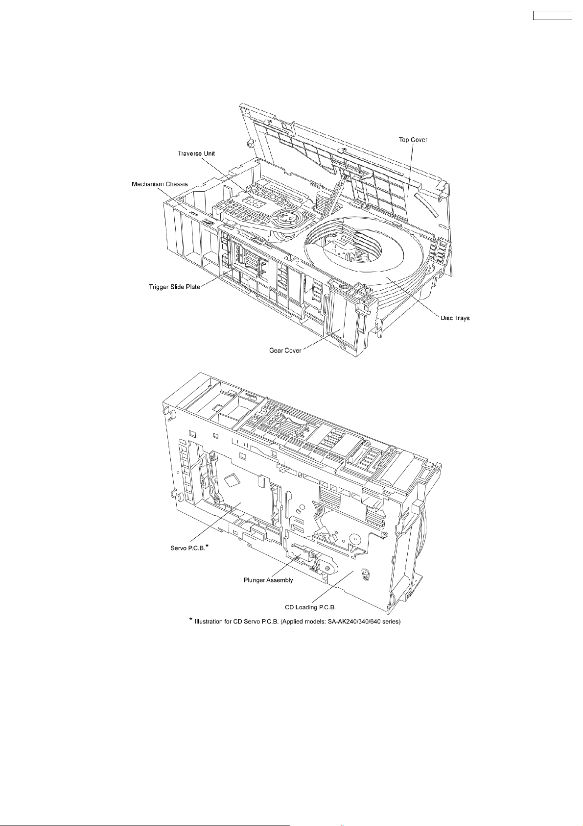
6 New Features
6.1. CRS1 Mechanism Overview
6.1.1. General Feature
· This is a five disc changer mechanism for CD/DVD. The outline figure is shown below.
7
Page 8
· The mechanism has "CHANGE WHILE PLAY" function. It open other trays for disc exchanging while one tray is at PLAY
position performing recording or reproducing.
· The mechanism can quickly change all trays with "CHANGE ALL" function. All trays can be move to OPEN position with one
operation.
· There is no sensor to indicate presence of disc on any tray.
6.1.2. Hardware composition
· Below is the hardware components of the mechanism
Name Function
Open Switch (OPEN-SW) The switch is used to detect normal tray opening
The switch is used for detect tray being manually push/trigger when full open
Home Switch (HOME-SW) Is used to detect cam gear home position
Close Sensor (CLOSE-SENSOR) Used for normal single tray closing
Used to detect cam gear rotate to Play Driving position
Play Switch (PLAY-SW) Detect TRV clamping complete position
Stocking Switch (STOCK-SW) Detect tray completely transfer for play position to stocking position
UD Sensor (UD-SENSOR) Detect TRV vertical movement position
Top Switch (TOP-SW) Detect a default position of TRV vertical movement position
Driver IC To drive Motor
Motor Main driving source for changer
Plunger Switching the driving source from motor to:
1. Tray open/close
2. Drive tray to play/stock position and TRV vertical movement
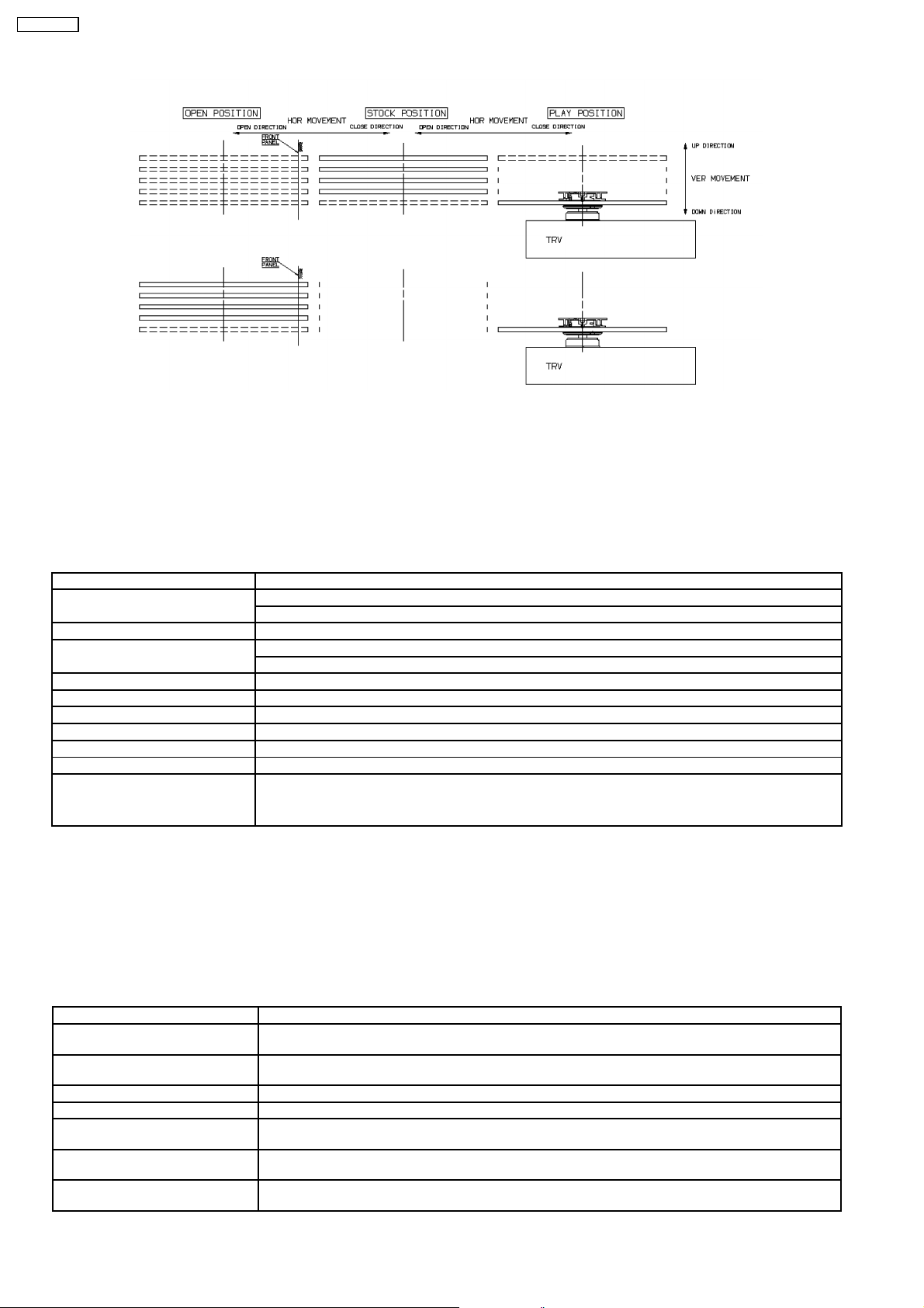
6.1.3. Mechanism Operation
· This mechanism has the following state:
1. Driving of a tray to open/close
2. Up/down operation of a traverse performs a state changes of tray.
By using the plunger to lift/release of a switching gear, and the cam gear to lift/release the function gear the motor can be link
to several gear trains to perform various operations.
· The functions that can be perform in this mechanism are described as below:
Condition Explanation
Open current playing tray The state to change current playing disc. All tray will be open at once and current tray at PLAY position
Open All The state where all trays being driven to OPEN position. The disc can be taken in or out from tray to tray
Stock The state where the trays are stored in STOCK position
Play The state where one of the tray 5 trays is being driven to PLAY position and clamped by traverse unit
Play & Open Tray-* The state where one of the tray is in playing position performing recording or reproducing, other trays can
Change The state when one of the opened tray being driven from OPEN position to STOCK position and other
Close All The state where all open trays will being driven from OPEN position to STOCK position, one by one from
will be expose.
by close tray one by one from top to bottom.
be used (OPEN position) for disc exchanging without stopping the recording or reproducing process.
opened trays remain still at OPEN position.
top to bottom
8
Page 9
Note: * represent tray number (from 1 ~ 5)
6.1.4. New CD Mechanism (CRS1)
Note:
This service manual does not contain the following information for the mention CD Mechanism drive:
· Schematic Diagram, Block Diagram and P.C.B. layout of CD Loading P.C.B.
· Part List for individual parts of the mechanism.
· Explode d View and Parts List for individual parts of the CD Mechanism drive.
Please refer to the original service manual (Order No. MD0509368C0) for the CD Mechanism Drive CRS1.
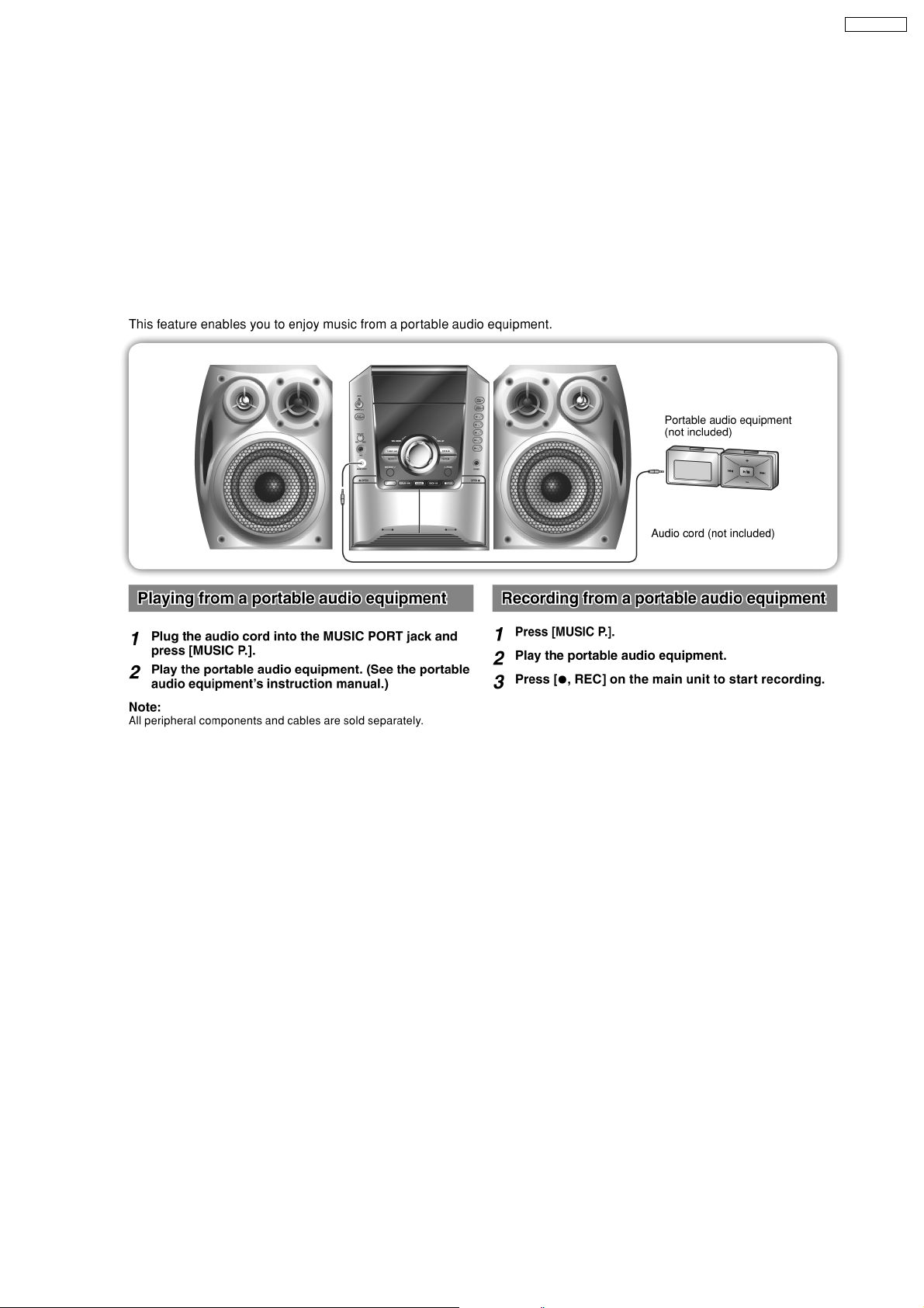
6.2. Music Port
With reference to page 17 of the operating instruction manual.
9
Page 10
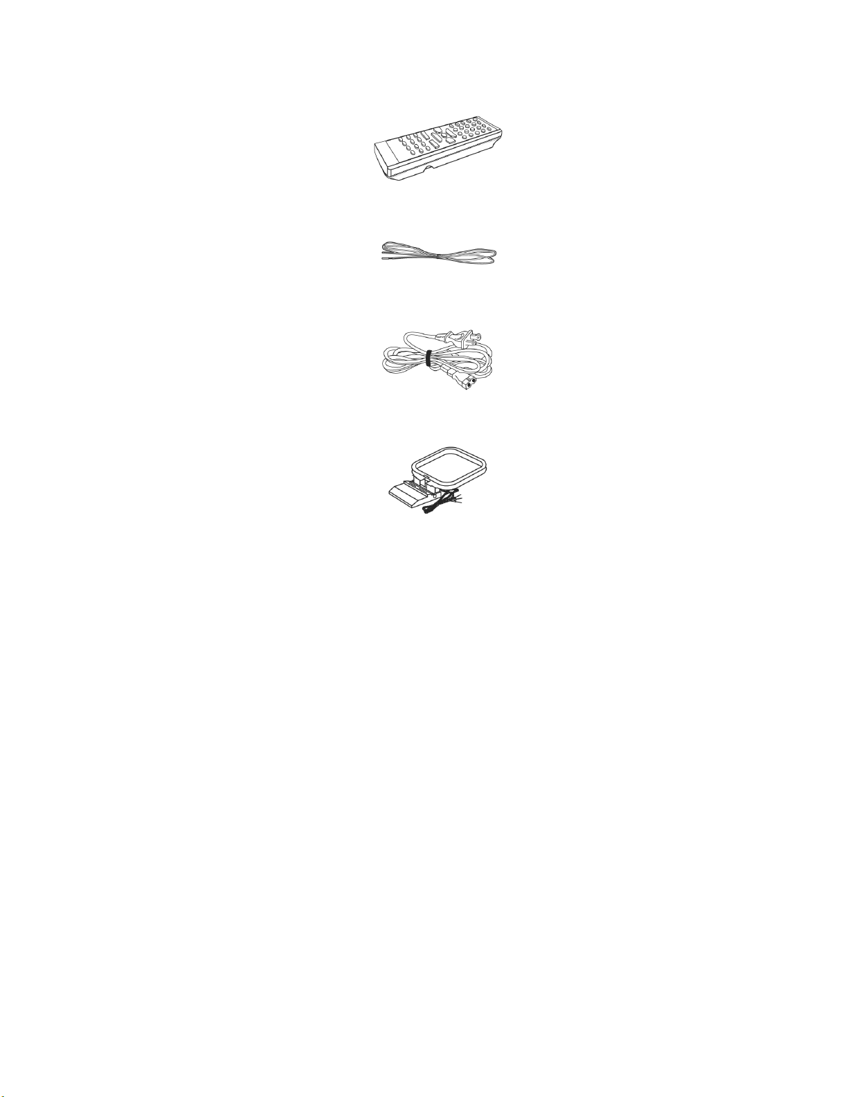
7 Accessories
Remote Control
N2QAHB000065
FM Antenna
Wire
RSA0006-L
AC Cord
SJA168-1A
AM Loop Antenna
N1DAAAA00001
Page 11
8 Operating Instructions Procedures
11
Page 12
12
Page 13
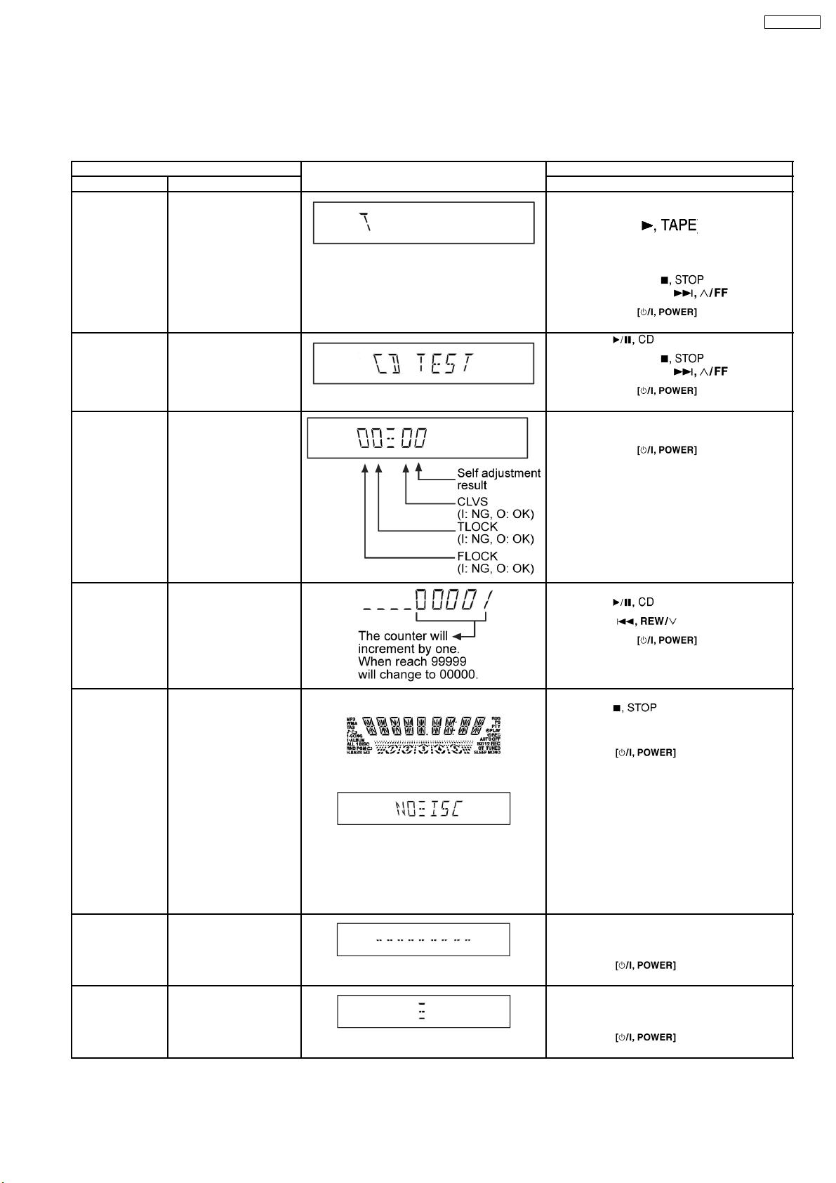
9 Self diagnosis and special mode setting
This unit is equipped with functions for checking and inspecting namely: Self-Diagnostic and Test Mode.
9.1. Special Mode Table
Item FL Display Key Operation
Mode Name Description Front Key
Self -Diagnostic
Mode
CD Test Mode To enter into checking the
CD Auto
Adjustment
To enter into self
diagnostic checking for
main unit.
reliability of changer unit.
To check the CD auto
adjustment result for
FLOCK, TLOCK and
CLVS.
1. Select [
] for TAPE mode (Ensure no tape is
inserted).
2. Press and hold [
seconds follow by [
To exit, press
main unit or remote control.
1. Select [ ] for CD mode.
2. Press and hold [
seconds follow by [
To exit, press
main unit or remote control.
In CD Test Mode:
1. Press [0] button on the remote control.
To exit, press
main unit or remote control.
]button for 3
].
button on
] button for 3
].
button on
button on
CD Changer
Reliability Test
(CRS1)
Doctor Mode To enter into Doctor
Cold Start To activate cold start
Changer
Reliability Test
To determine the
reliability of CD Changer
Unit.
(For more information,
refer to section 9.1.1)
Mode for checking of
various items and
displaying EEPROM and
firmware version.
upon next AC power up.
To check the function
operation of changer unit.
(For more information,
refer to 9.1.1)
1.
2.
1. All segments will light up for 1 second.
2. The Check Sum of EEPROM and firmware
version will be display.
* ROM correction
** Firmware version No:
In Self-Diagnostic Mode:
1. Select [
2. Press [
To exit, press
main unit or remote control.
(The tray will return to PLAY position and then
power off)
In any mode:
1. Press [
follow by [4] and [7] on remote control.
To exit, press [ENTER] button on remote
control or
unit or remote control.
In doctor mode:
1. Press [4] button on remote control.
To exit, press [ENTER] button on remote
control or
unit or remote control.
In doctor mode:
1. Press [DISC] on remote control.
To exit, press [ENTER] button on remote
control or
unit or remote control.
] for CD mode.
] button.
button on
] button on main unit
button on main
button on main
button on main
13
Page 14
Item FL Display Key Operation
Mode Name Description Front Key
FL Display Test To check the FL
segments display (All
segments will light up and
LED will blink at 0.5
second interval)
Tape Eject Test To check on the tape
eject function (For deck
1/2)
In doctor mode:
1. Press [PROGRAM] button on remote
In doctor mode:
1. Press [PROGRAM] button on remote
9.1.1. CD changer unit ageing test mode
Below is the process flow chart of ageing for the CD changer unit. (CRS1)
control.
control.
14
Page 15
9.2. Error code Table
Self-Diagnosis Function (refer Section 9.1) provides information on any problems occuring for the unit and its respective
components by displaying the error codes. These error code such as U**, H** and F** are stored in memory and held unless it is
cleared.
15
Page 16
The error code is automatically display after entering into self-diagnostic mode.
Error Code Diagnosis Contents Description of error Automatic FL Display Remarks
H01 Mode SW, plunger
and capstan motor
abnormal
For deck mechanism unit (For deck 1/2).
Press [
next error.
] on main unit for
H02 Rec INH SW
H03 HALF SW abnormal For deck mechanism unit (For deck 1/2).
F01
F02
F15 RESET SW
F26 Transmission error
F61 Power Amp IC output
IHMS Cam gear
abnormal
Reel pulse abnormal
TPS error
abnormal
between CD Servo
LSI IC and
microprocessor IC
abnormal
abnormality
REST SW: ON is not
detected within the
specified time.
When set to CD mode,
the sense signal does
not turn “Low”, a fail
safe time after system
command
transmission is sent.
Upon power on,
PCONT=HIGH,
DCDET=L after
checking LSI.
Cam gear does not
rotate to “HOME”
position.
For deck mechanism unit (For deck 2).
Press [
next error.
Press [
next error.
For deck mechanism unit (For deck 1/2).
Press [
next error.
For CD unit (For Traverse).
Press [
next error.
For CD unit (For Traverse).
Press [
next error.
For power.
Press [
next error.
For CD changer unit (CRS1).
Press [SINGLE CHANGE] on main unit
for next error.
] on main unit for
] on main unit for
] on main unit for
] on main unit for
] on main unit for
] on main unit for
ICSL Cam gear/gear units
abnormal
ISTK Drive rack/gear
assembly abnormal
IPLY Drive rack/gear
assembly abnormal
Cam gear does not
rotate to “PLAY”
driving position and
hence does not drive
playing tray to
“STOCK” position.
The tray drive rack
does not move to
“STOCK” position.
(Tray does not move
to “STOCK” position)
The tray drive rack
does not move to
“PLAY” position. (Tray
does not move to
“PLAY” position)
For CD changer unit (CRS1).
Press [SINGLE CHANGE] on main unit
for next error.
For CD changer unit (CRS1).
Press [SINGLE CHANGE] on main unit
for next error.
For CD changer unit (CRS1).
Press [SINGLE CHANGE] on main unit
for next error.
16
Page 17
Error Code Diagnosis Contents Description of error Automatic FL Display Remarks
ITOP UD assembly UD Rack does not
move to front
direction. This lead to
UD base not raise to
top position.
For CD changer unit (CRS1).
Press [SINGLE CHANGE] on main unit
for next error.
IUDS UD assembly After TOP SW is
HOME Cam gear/gear
assembly abnormal
LOAD Tray drive assembly
abnormal
PDRV Cam gear/gear
assembly abnormal
detected, UD rack
does not move into
tray 1 position.
Cam gear does not
move to “HOME”
position under
following conditions
1. After tray is load to
“PLAY” position.
2. After tray is unload
to “STOCK”
position.
Tray unit does not
move from “STOCK”
to “PLAY” position
Cam gear does not
move from “HOME” to
“PLAY” drive position.
For CD changer unit (CRS1).
Press [SINGLE CHANGE] on main unit
for next error.
For CD changer unit (CRS1).
Press [SINGLE CHANGE] on main unit
for next error.
For CD changer unit (CRS1).
Press [SINGLE CHANGE] on main unit
for next error.
For CD changer unit (CRS1).
Press [SINGLE CHANGE] on main unit
for next error.
UDU UD base asssembly
abnormal
UDD UD base asssembly
abnormal
UD1 UD base asssembly
abnormal
F1NG Fail - safe mode. (For
open/close tray
unit(s))
UD Base assembly
does not move
upwards from tray 5 to
tray 2
UD Base assembly
does not move
downwards from tray 1
to tray 5.
UD Base assembly
does not move to tray
1.
When the tray open
operation is
performed, it fails to
open. It will
automatically close all
trays after the time-out
by the microprocessor.
During this time when
it fails, the error code
will appear.
For CD changer unit (CRS1).
Press [SINGLE CHANGE] on main unit
for next error.
For CD changer unit (CRS1).
Press [SINGLE CHANGE] on main unit
for next error.
For CD changer unit (CRS1).
Press [SINGLE CHANGE] on main unit
for next error.
For CD changer unit (CRS1).
Press [SINGLE CHANGE] on main unit
for next error.
17
Page 18
Error Code Diagnosis Contents Description of error Automatic FL Display Remarks
F2NG Fail - safe mode. (For
open/close tray
unit(s))
SRVC_TRV To unlock the
traverse unit for
service
RSET Cam gear jam/close
sensor faulty
When the tray close
operation is
performed, it fails to
close. It will
automatically open all
trays after the time-out
by the microprocessor.
During this time when
it fails, the error code
will appear.
1. All trays set to
“STOCK” position
2. Mechanism set to
tray 5
3. Cam gear set to
“HOME” position
During tray re-open,
the cam gear will
rotate in the opposite
direction to reset the
cam gearposition.
When it fails, the error
code will appear.
For CD changer unit (CRS1).
Press [SINGLE CHANGE] on main unit
for next error.
For CD changer unit (CRS1).
Press [SINGLE CHANGE] on main unit
for next error.
For CD changer unit (CRS1).
Press [SINGLE CHANGE] on main unit
for next error.
CRS1 Error Code display
1. The errors that occured in CRS1 Mechanism can be recalled and displayed, in the order of the occurence under self-diagnostic
(Refer to Section 9.1 for procedures to enter this mode.
· Only the first 5 errors will be memorized (in backup memory). The subsequence error shall be ignored and not memorize.
For system with EEPROM as memory backup,memory space in EEPROM is neccesary.
2. To display all error code memorized
In CRS1 Self-Diagnostic mode, press [SINGLE CHANGE] to display subsequence error code.
It shall repeat after reaching error no. 5.
e.g.:
[1____IHMS]→ [SINGLE CHANGE]
[2____ITOP]→ [SINGLE CHANGE]
[3____HOME]→ [SINGLE CHANGE]
[4____LOAD]→ [SINGLE CHANGE]
[5_____UDD]→ [SINGLE CHANGE]
3. To clear the error code memory
In CRS1 Self-Diagnostic mode, long press [SINGLE CHANGE] key (2s or more)1
18
Page 19
10 Assembling and Disassembling
10.1. Caution
Special Note:
This model uses a new CD changer unit CRS1. In this following section does not contain the necessary disassembly &
assembly information for the CD changer unit (CRS1) except the disasembly & assembly of traverse unit. Kindly refer to the
original service manual for the CD changer unit. (Order No. MD050 9368C0).
“ATTENTION SERVICER”
Some chassis components may have sharp edges. Be careful when disassembling and servicing.
1. This section describes procedures for checking the operation of the major printed circuit boards and replacing the main
components.
2. For reassembly after operation checks or replacement, reverse the respective procedures.
Special reassembly procedures are described only when required.
3. Select items from the following index when checks or replacement are required.
4. Refer to the Parts No. on the page of “Parts Location and Replacement Parts List” (Section 22), if necessary.
Warning :-
This product uses a laser diode. Refer to caution statement Precaution of Laser Diode.
Caution:
After replacing of CD Changer Unit, ageing test is necessary. Please confirm operation for CD Changer Unit.
Below is the list of disassembly sections
· Disasse mbly of Top Cabinet
· Disasse mbly of Rear Panel
· Disasse mbly of CD Changer Unit
· Disasse mbly of Main P.C.B.
· Disasse mbly of Transformer P.C.B.
· Disasse mbly of Power P.C.B.
· Disasse mbly of Front Panel Unit
· Disasse mbly of Panel P.C.B.
· Disasse mbly of Deck Mechanism Unit
· Disasse mbly for Deck P.C.B.
· Disasse mbly of Traverse Unit
· Disasse mbly of Optical Pickup Unit (CD Mechanism)
· Disasse mbly of Deck Mechanism
· Replacement for cassette lid
· Rectification for tape jam problem
19
Page 20
10.2. Disassembly flow chart
The following chart is the procedure for disassembling the casing and inside parts for internal inspection when carrying out the
servicing.
To assemble the unit, reverse the steps shown in the chart as below.
20
Page 21
10.3. Main Parts Location
21
Page 22
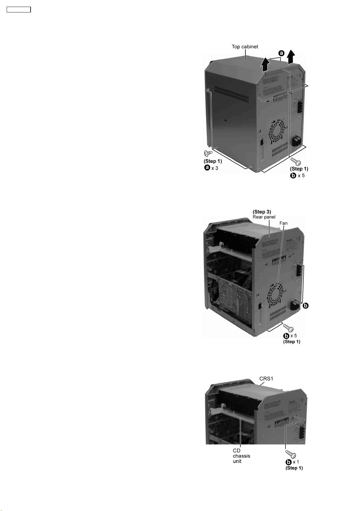
10.4. Disassembly of Top Cabinet
Step 1 Remove 3 screws at each side and 5 screws at rear
panel.
Step 2 Lift up both sides of the top cabine t, push the top
cabinet towards the rear to remove the top cabinet.
10.5. Disassembly of Rear Panel
· Follow the (Step 1) - (Step 2) of Item 10.4 - Disassembly of Top Cabinet
Step 1 Remove 5 screws.
Step 2 Disconnect cable CN2810 (Fan) at Main P.C.B..
Step 3 Remove rear panel.
10.6. Disassembly of CD Changer Unit (CRS1)
· Follow the (Step 1) - (Step 2) of Item 10.4 - Disassembly of Top Cabinet
Step 1 Remove 1 screw at rear panel.
22
Page 23
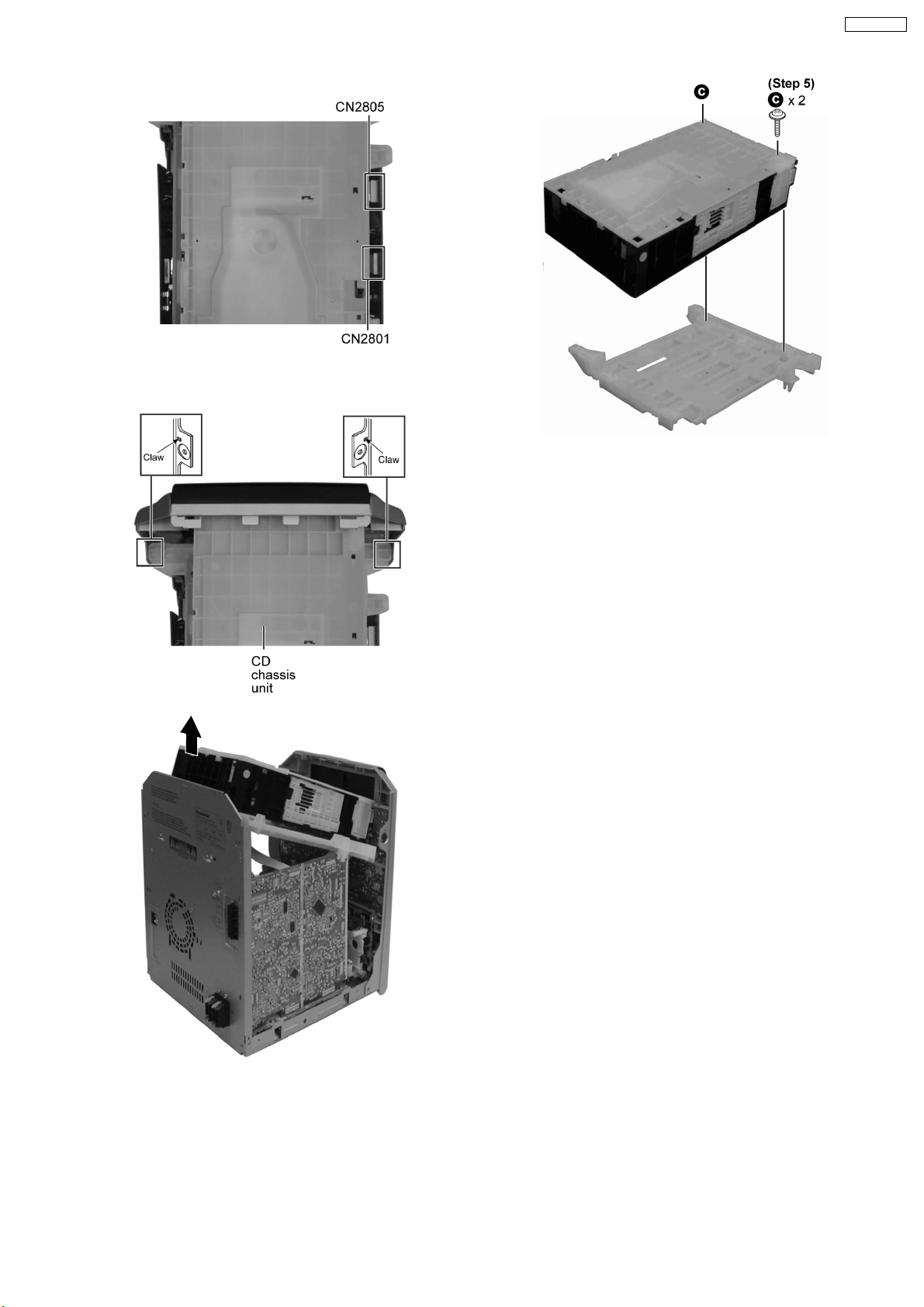
Step 2 Detach the FFC cables (CN2801 & CN2805).
Step 3 Release the claws on both ends.
Step 5 Remove 2 screws.
Step 6 Remove the Mecha Chassis.
Note:
For disassembly & assembly of traverse unit, please refer to
section 10.14 of this service manual.Please refer to original
Service Manual for the Disassembly and Assembly of the CD
Changer Unit (CRS1).
Step 4 Lift the CD changer unit upwards to remove it.
· Disasse mbly of Mecha Chassis
23
Page 24
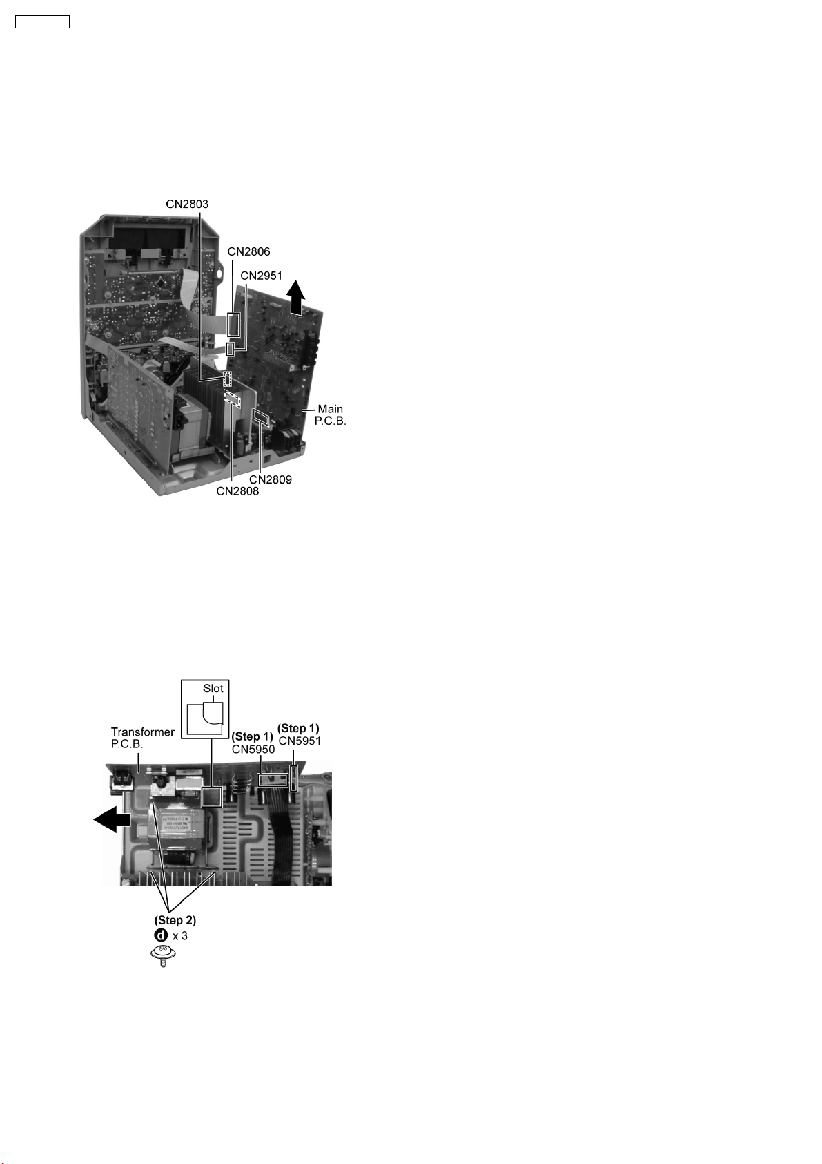
10.7. Disassembly of Main P.C.B.
· Follow the (Step 1) - (Step 2) of Item 10.4 - Disassembly of Top Cabinet
· Follow the (Step 1) - (Step 4) of Item 10.6 - Disassembly of CD Changer Unit
· Follow the (Step 1) - (Step 3) of Item 10.5 - Disassembly of Rear Panel
Step 1 Disconnect FFC cables (CN2803, CN2806 and
CN2951).
Step 2 Detach connectors (CN2808 & CN2809).
Step 3 Remove Main P.C.B..
10.8. Disassembly of Transformer P.C.B.
· Follow the (Step 1) - (Step 2) of Item 10.4 - Disassembly of Top Cabinet
· Follow the (Step 1) - (Step 3) of Item 10.5 - Disassembly of Rear Panel
· Follow the (Step 1) - (Step 4) of Item 10.6 - Disassembly of CD Changer Unit
Step 1 Disconnect connectors (CN5950 & CN5951).
Step 2 Remove 3 screws (Mounting screws for transformer to
bottom chassis).
Step 3 Push the Transformer P.C.B. sidewards to remove it.
24
Page 25
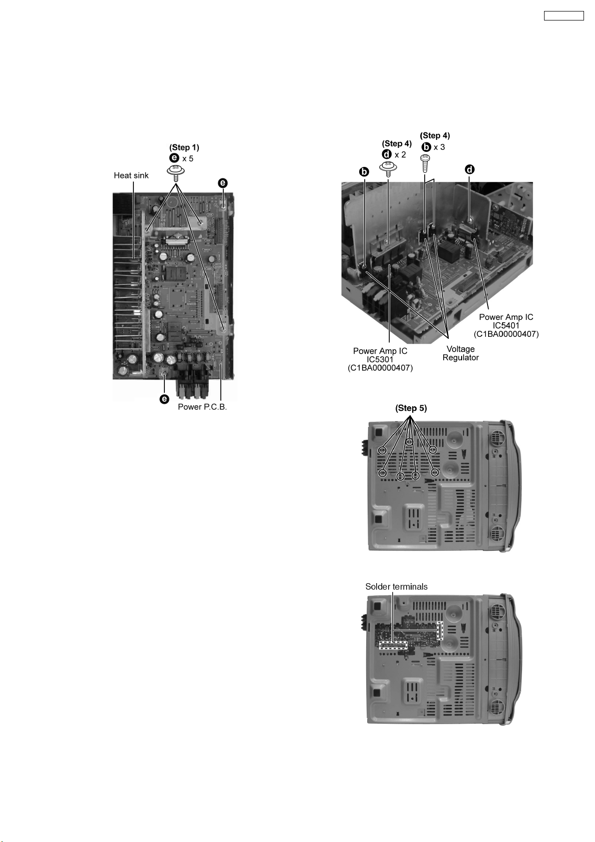
10.9. Disassembly of Power P.C.B.
· Follow the (Step 1) - (Step 2) of Item 10.4 - Disassembly of Top Cabinet
· Follow the (Step 1) - (Step 4) of Item 10.6 - Disassembly of CD Changer Unit
· Follow the (Step 1) - (Step 3) of Item 10.5 - Disassembly of Rear Panel
· Follow the (Step 1) - (Step 3) of Item 10.7 - Disassembly of Main P.C.B.
Step 1 Remove the 5 screws on Power P.C.B..
Step 2 Detach cable (CN5950) remove the 5 screws on Power
P.C.B..
Step 3 Remove Power P.C.B..
Note:
Insulate the Power P.C.B. with insulation material to avoid short
circuit.
· Replacement of the Power Amp IC or Voltage Regulator
Step 4 Remove 2 screws at the Power Amp IC and/or 3
screws to Voltage Regulator.
Step 5 Cut the joints with a metal cutter as shown below.
Step 6 Desolder the terminals to replace the components.
Step 7 Fix back the cut portion with a screw as shown.
25
Page 26
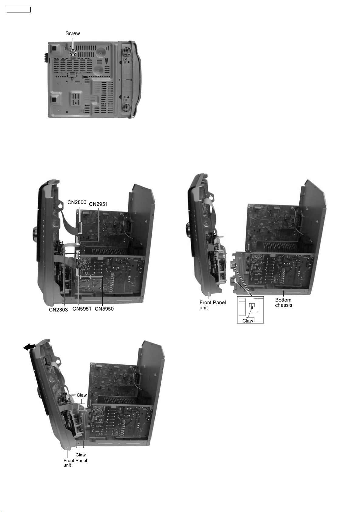
10.10. Disassembly of Front Panel Unit
· Follow the (Step 1) - (Step 2) of Item 10.4 - Disassembly of Top Cabinet
· Follow the (Step 1) - (Step 4) of Item 10.6 - Disassembly of CD Changer Unit
Step 1 Disconnect connectors (CN2803, CN2806, CN2951,
CN5950 & CN5951).
Step 3 Release 2 claws outwards.
Step 2 Bent the front panel unit slightly forward as arrow
shown.
Step 4 Remove the front panel unit.
Note: Ensure 2 claws located at the bottom chassis is seated
into the 2 slots at bottom of front panel at 2 catches (one on
each side) of bottom chassis to be aligned to front panel’s slot.
Assembly is secured upon hearing clicking sound.
26
Page 27
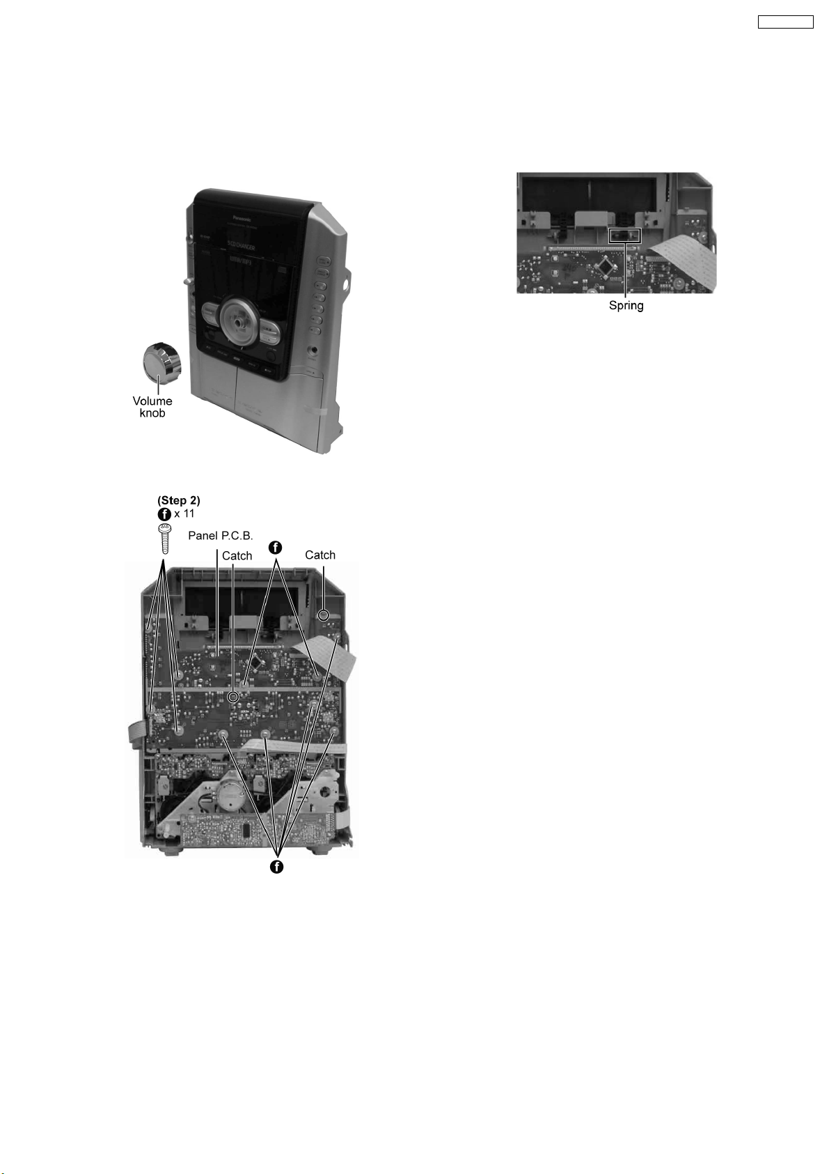
10.11. Disassembly for Panel P.C.B.
· Follow the (Step 1) - (Step 2) of Item 10.4 - Disassembly of Top Cabinet
· Follow the (Step 1) - (Step 4) of Item 10.6 - Disassembly of CD Changer Unit
· Follow the (Step 1) - (Step 4) of Item 10.10 - Disassembly of Front Panel Unit
Step 1 Remove the volume knob.
Step 2 Remove Lid.
Note: Do not misplace the spring.
Step 2 Remove 11 screws.
Step 3 Release 2 catches.
Step 4 Remove Panel P.C.B..
10.11.1. Disassembly of Lid
Step 1 Lift the spring sideward.
27
Page 28
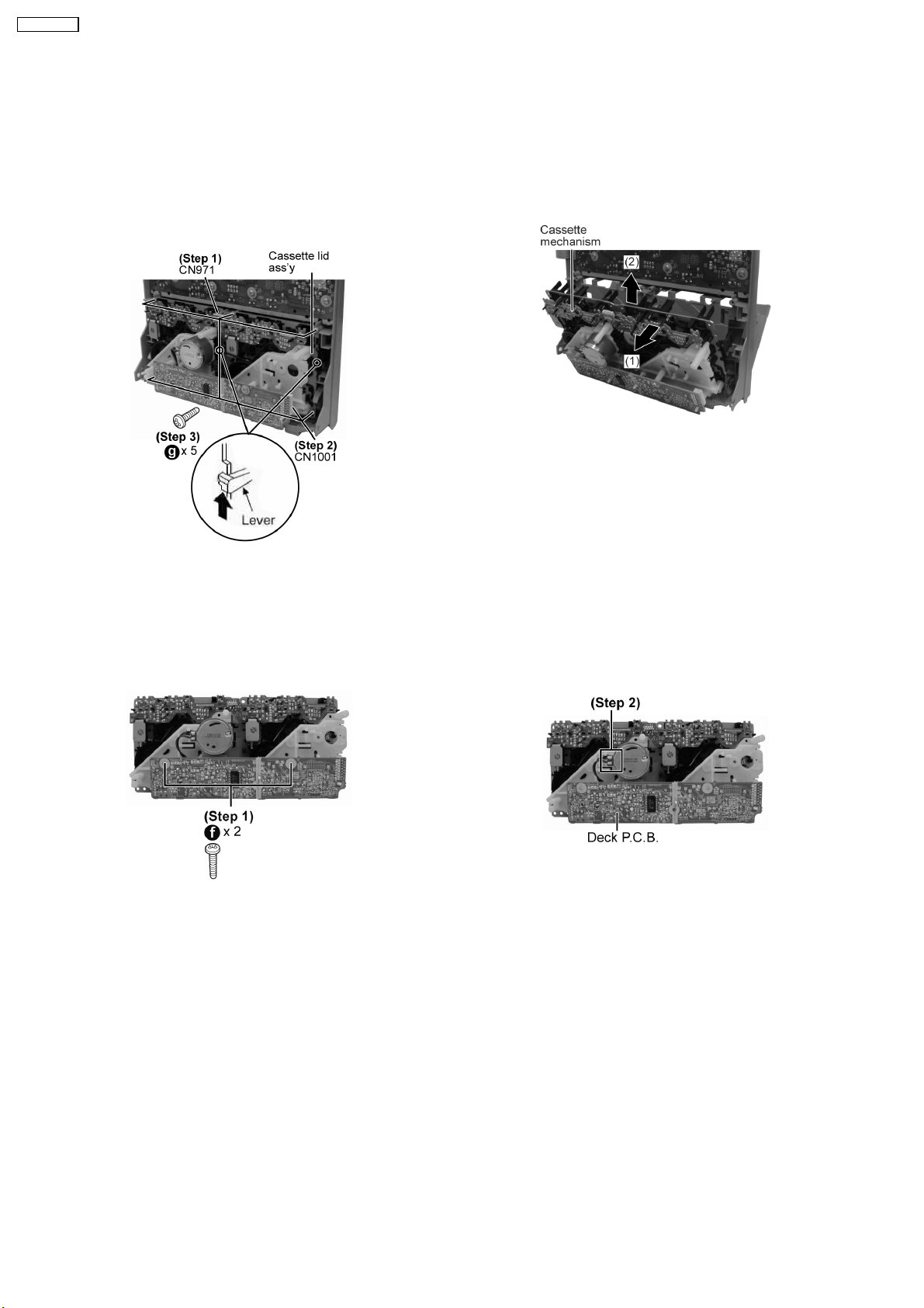
10.12. Disassembly of Deck mechanism unit
· Follow the (Step 1) - (Step 2) of Item 10.4 - Disassembly of Top Cabinet
· Follow the (Step 1) - (Step 4) of Item 10.6 - Disassembly of CD Changer Unit
· Follow the (Step 1) - (Step 4) of Item 10.10 - Disassembly of Front Panel Unit
Step 1 Detach FFC cable (CN971).
Step 2 Disconnect FFC cable (CN1001).
Step 3 Remove the 5 screws.
Step 4 Push the lever upward, and then open the cassette lid
ass’y (For DECK1 and DECK2).
Step 5 Tilt the cassette mechanism unit in the direction of
arrow (1), and then remove it in the direction of arrow (2).
Note: For disassembly of parts for deck mechanism unit,
refer to Section 10.15.
10.13. Disassembly of Deck P.C.B.
· Follow the (Step 1) - (Step 2) of Item 10.4 - Disassembly of Top Cabinet
· Follow the (Step 1) - (Step 4) of Item 10.6 - Disassembly of CD Changer Unit
· Follow the (Step 1) - (Step 4) of Item 10.10 - Disassembly of Front Panel Unit
Step 1 Remove 2 screws.
Step 2 Desolder wire at deck motor terminals (W1002).
Step 3 Remove Deck P.C.B.
10.14. Disassembly of Traverse Unit
· Follow the (Step 1) - (Step 2) of Item 10.4 - Disassembly of Top Cabinet
· Follow the (Step 1) - (Step 4) of Item 10.6 - Disassembly of CD Changer Unit22
Important notes: Ensure all the trays are in the “STOCK”
position before proceeding to the disassemble of traverse
unit. For procedures to set the trays in “STOCK” position,
please refer to original Service Manual for CRS1, Section 7.
Disassembling Procedure When Tray In Play Position,
Order No. MD0509368C0.
28
Page 29
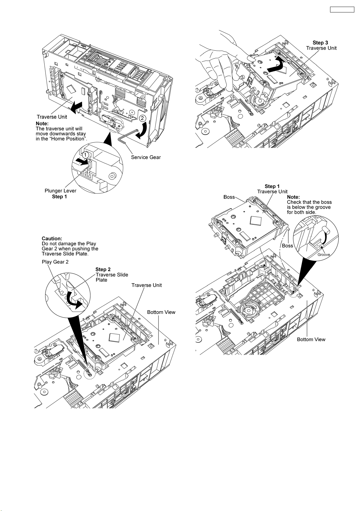
Step 1: Press and hold the plunger lever and rotate the
gear as arrows shown until it stop.
Step 3: Remove the traverse unit as arrow shown.
· Assembly of Traverse Unit
Step 2: Push the traverse slide plate as arrow shown to
release the traverse unit.
Caution: Do not exert strong force on the traverse
slide plate.
Step 1: Turn over the unit and install the traverse unit.32
29
Page 30
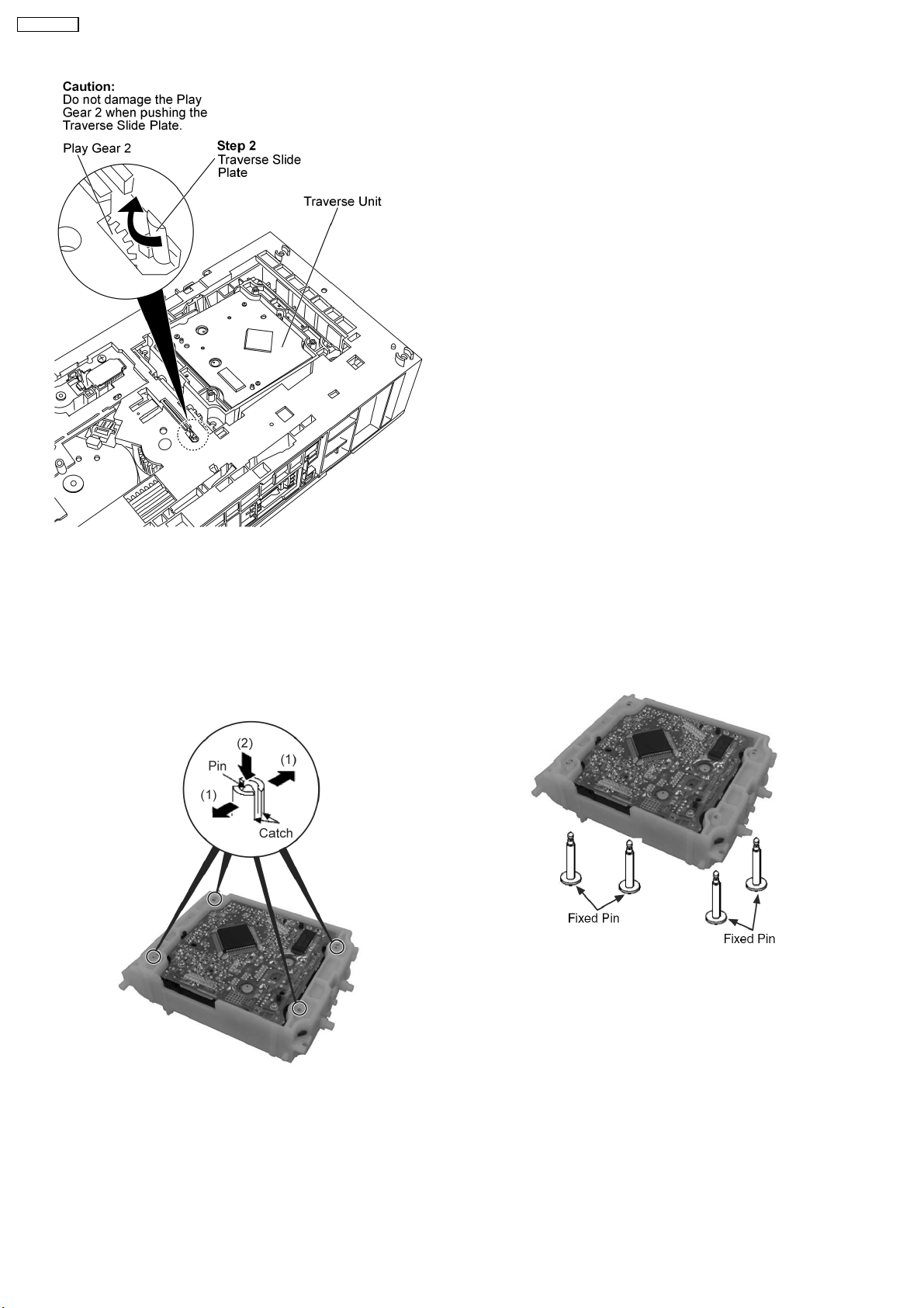
Step 2: Push the traverse slide plate as arrow shown to
lock the traverse unit.
10.15. Disassembly of optical pickup unit (CD mechanism)
· Follow the (Step 1) - (Step 2) of Item 10.4 - Disassembly of Top Cabinet
· Follow the (Step 1) - (Step 4) of Item 10.6 - Disassembly of CD Changer Unit
· Follow the (Step 1) - (Step 2) of Item 10.14 - Disassembly of Traverse Unit
Step 1 Pull out FFC.
Step 3 Remove 4 pins.
Step 2 Widening the catch, push the pin in.
30
Page 31

Step 4 Remove the traverse deck.
Note: As floating springs (4 pieces) come off at the same time,
be careful not to lose them.
Step 8 Remove the catch of the drive rack, and take out the
drive rack.
Step 5 Remove 3 screws.
Step 6 Remove the CD Servo P.C.B. and turn it over.
Note: Insert a short pin into FFC of the optical pickup.
Step 7 Rotate the traverse deck (B) to the arrow direction and
shift the optical pickup to the furthest backward.
Step 9 Place the convex part of an optical pickup to the
concave part of a traverse base, then take out the optical
pickup.
31
Page 32

10.16. Disassembly of Deck Mechanism
· Follow the (Step 1) - (Step 2) of Item 10.4 - Disassembly of Top Cabinet
· Follow the (Step 1) - (Step 4) of Item 10.6 - Disassembly of CD Changer Unit
· Follow the (Step 1) - (Step 4) of Item 10.10 - Disassembly of Front Panel Unit
· Follow the (Step 1) - (Step 5) of Item 10.12 - Disassembly of Deck Mechanism Unit
10.16.1. Disassembly of the pinch roller ass’y and head block
* The mechanism as shown below is for DECK1. For DECK
2, perform the same procedures.
32
Page 33

Step 1 Release the catch, and then remove the pinch roller (F).
Step 2 Release 2 claws and detach the head block connector.
Step 3 Remove 2 screws.
Step 4 Remove head block.
10.16.2. Disassembly of capstan motor ass’y, capstan belt A, capstan belt B and winding
belt
Step 1 Detach the head block connector (Deck P.C.B.).
Step 2 Desolder wire(W1002) at motor assembly.
Step 3 Remove Deck P.C.B.
Step 4 Remove 3 screws (for deck 1 & 2).
Step 5 Remove capstan belt A/B.
Step 6 Remove the flywheel R.
Step 7 Release the claw and remove the winding lever and
spring.
[Installation of the belt]
Step 1 The boss and marking should be positioned
horizontally.
33
Page 34

Step 2 Put the winding belt on the pulley temporarily.
Step 3 Install the flywheel F.
Step 4 Put the winding belt on the flywheel F.
Step 5 Install the winding lever and spring while pressing the
winding arm in the direction of arrow.
Step 6 Install the flywheel R.
Step 7 Put the capstan belt A temporarily as shown below.
Step 8 Put the capstan belt B on the motor ass’y pulley.
Step 9 Install the sub chassis to the mechanism, and then
tighten screws.
34
Page 35

Step 10 Install 3 screws.
Step 11 Put the capstan belt B as shown below.
Step 12 Put the capstan belt A on the motor ass’y pulley.
35
Page 36

10.17. Replacement for cassette lid
· Follow the (Step 1) - (Step 2) of Item 10.4 - Disassembly of Top Cabinet
Step 1 Lift up the lever upward, open the cassette deck. (For
DECK1 and DECK2)
Step 2 Push up the cassette lid (L/R) in the direction of arrow.
(For DECK1 and DECK2).
10.18. Rectification for tape jam problem
· Follow the (Step 1) - (Step 2) of Item 10.4 - Disassembly of Top Cabinet
Step 1 If a cassette tape cannot be removed from the deck (the
tape is caught by the capstan or pinch roller during playback or
recording), rotate the flywheel F in the direction of the arrow to
remove it.
Step 2 Push the lever upward and open the cassette lid.
Remove the cassette tape.
36
Page 37

37
Page 38

11 Service Fixture and Tools
38
Service Tools
Extension FFC
(A) Deck P.C.B. - Main P.C.B. REEX0485 (14 Pins)
(B) Panel P.C.B. - Deck Mechanism P.C.B. REEX0484 (10 Pins)
12 Service Positions
Note: For description of the disassembly procedures, see the Section 10.
12.1. Checking and Repairing of Main P.C.B.
Page 39

12.2. Checking and Repairing of Transformer P.C.B.
39
Page 40

12.3. Checking and Repairing of Panel, Deck & Deck Mechanism P.C.B.
40
Page 41

12.4. Checking and Repairing of Power P.C.B.
41
Page 42

13 Adjustment Procedures
42
13.1. Cassette Deck Section
· Measurement Condition
−
− Reverse-mode selector switch:
− −
−
− Deck Tape Select: NORMAL
− −
−
− Make sure head, capstan and press roller are clean.
− −
−
− Judgeable room temperature 20 ± 5 °C (68 ± 9°F)
− −
· Measuring instrument
−
− EVM (DC Electronic voltmeter)
− −
−
− Digital frequency counter
− −
· Test Tape
−
− Tape speed gain adjustment (3 kHz, -10 dB);
− −
QZZCWAT
13.1.1. Tape Speed Adjustment (Deck 1/2)
1. Insert the test tape (QZZCWAT) to DECK 2 and playback
(FWD side) the middle portion of it.
2. Adjust Motor VR (DECK 2) for the output value shown
below.
Adjustment target: 2910 ~ 3090 Hz (NORMAL speed)
3. After alignment, assure that the output frequency of the
DECK 1 FWD are within ±60 Hz of the value of the output
frequency of DECK 2 FWD.
13.1.2. Bias Voltage Check
1. Set the unit “AUX” position.
2. Insert the Normal blank tape (QZZCRA) into DECK 2 and
the unit to “REC” mode (use “l REC/STOP” key).
3. Measure and make sure that the output is within the
standard value.
Bias voltage for Deck 2 14±4mV (Normal)
Fig. 2
Fig. 3
Fig. 1
13.1.3. Bias Frequency Adjustment (Deck 1/2)
1. Set the unit to “AUX” position.
2. Insert the Normal blank tape (QZZCRA) into DECK 2 and set the unit to “REC” mode (l use “REC/STOP” key).
3. Adjust L1002 so that the output frequency is within the standard value as below.
Standard Value: 89 ~ 110 kHz
Fig. 4
13.1.3.1. Cassette Deck Section
Below is the locations of test points for Deck P.C.B.:-
Page 43

13.2. Tuner Section
43
This section include details on the alignment of AM-IF and AM RF adjustment.
13.2.1. AM-IF Alignment
1. Set up the equipments as shown in Fig. 5.
2. Select [TUNER] mode on selector and set to [AM] mode.
3. Apply signal as shown in Fig. 5 from AM-SG.
4. Adjust Z2602 accordingly so that the output frequency is maximized at 450kHz in Fig. 6.
Fig. 5
Fig. 6
13.2.2. AM RF Adjustment
1. Set up the equipments as shown in Fig. 7.
2. Select [TUNER] on selector and set to [AM] mode.
3. Set AM-SG to 520kHz.
4. Receive 520kHz in the unit.
5. Adjust L2601 (OSC) so that the EVM-AC is maximized.
6. Set AM-SG to 600Hz.
7. Receive 600Hz in the unit.
8. Adjust L2601 (ANT) so that the EVM-SG is maximized.
9. Set AM-SG to 520kHz.
10. Receive 520kHz in the unit.
11. Adjust L2602 (OSC) so that the EVM-DC value is with 1.1±0.5V.
Page 44

Fig. 7
44
13.2.3. Adjustment Point
Below is the locations of alignment points on the Main (Tuner) P.C.B.
Page 45

14 Voltage and Waveform Chart
45
Note:
Circuit voltage and waveform described herein shall be regarded as reference information when probing defect point, because it
may differ from an actual measuring value due to difference of Measuring instrument and its measuring condition and product itself.
14.1. CD Servo P.C.B. & Main P.C.B.
Page 46

46
Page 47

14.2. Power P.C.B. and Transformer P.C.B.
47
Page 48

14.3. Waveform Chart
48
Page 49

49
Page 50

15 Wiring Connection Diagram
50
PHONE
9. . . . . .1
H6555/
W6555
JK6551
PbF
12
. . . . . . . .
1
CN2809
CN2808
12
. . . . . . . .
1
CN2803
14 . . . . . . .2
13 . . . . . . .1
MAIN P.C.B
B
SOLDER SIDE
CN2951
10 . . . 2
9 . . . 1
FM ANT
TUNER PACK
FAN
MOTOR
CN2806
30 . . . . . . . . . . . . 2
29 . . . . . . . . . . . . .1
AM ANT
TUNER PACK
H
P.C.B
BLACK
RED
To CRS1 (CN1)
JK2601
2
1
(To Fan)
CN2810
CN2801
2
. . . . . .
16
CN2805
15
1 2
1
. . . . . . . .
17
. . . . . . . . . .
14
. . . . . . .
2
1
CN5103
1
. . . . . . . . .
12
CN5102
1
. . . . . . . . .
12
JK5102 JK5101
LEFT
SPEAKER
E
POWER P.C.B
SOLDER SIDE
RIGHT
SPEAKER
H5104/
W5104
9
. . . . . . . .
1
PbF
PbF
SENSOR
VOLUME
CS1002
1
5
3
4
2
(DECK 2)
R/P HEAD
JK6751
MUSIC
PORT
MOTOR
-
+
2
1
W1002
Z6481
C
PANEL P.C.B
SOLDER SIDE
VR6491
JK6501 VR6511
MIC VOL
MIC
PbF
DECK MECHANISM P.C.B
G
SOLDER SIDE
F
CN6601
1
. . . . . . . . . . . . . . . . . . . .
2
. . . . . . . . . . . . . . . . . . . .
29
30
1 . . . 9
2 . . . 10
CN971
DECK P.C.B
SOLDER SIDE
PbF
PLAYBACK HEAD
CS1001
12345
(DECK 1)
PbF
CN5951
1
. . . . . . .
9
9 . . . . . . . . .1
CN5950
TRANSFORMER P.C.B
D
SOLDER SIDE
CN1001
2
1
. . . . . . . . . .
. . . . . . . . . .
14
13
CN7002
17
. . . . . . . . . . . .
16
. . . . . . . . .
2
1
M
TRAVERSE
MOTOR
T5950
(POWER TRANSFORMER)
A
CD SERVO P.C.B
SOLDER SIDE
M7301
SPINDLE MOTOR
CAUTION
RISK OF ELECTRIC SHOCK
AC VOLTAGE LINE.
PLEASE DO NOT TOUCH
THIS P.C.B
T5951
(SUB-TRANSFORMER)
. . . . . . . . . . .
15
16
M
M7302
CN7001
JK5950
2
1
. . . . . . . . . . .
PbF
AC IN
120V 60HZ
OPTICAL PICKUP
Page 51

margaiDkcolB 61
51525354555657
Page 52

Page 53

Page 54

Page 55

Page 56

Page 57

Page 58

58
Page 59

17 Schematic Diagram
59
(All schematic diagrams may be modified at any time with the
development of the new technology)
17.1. Notes of Schematic Diagrams
S951 : MODE Switch
S952 : HALF Switch
S971 : MODE Switch
S972 : HALF Switch
S975 : RECINH_F Switch
S6101 : POWER Switch
S6102 : SINGLE DISC CHANGE Switch
S6103 : OPEN/CLOSE Switch
S6104 : CD1 Switch
S6105 : CD2 Switch
S6106 : CD3 Switch
S6107 : CD4 Switch
S6108 : CD5 Switch
S6201 : DECK 2 OPEN Switch
S6202 : DISPLAY/DEMO Switch
S6203 : DECK 1/2 Switch
S6204 : H.BASS Switch
S6205 : FF Switch
S6206 : REW Switch
S6207 : DECK 1 OPEN Switch
S6301 : CD Switch
S6302 : TAPE Switch
S6303 : STOP Switch
S6304 : REC Switch
S6305 : TUNER/BAND Switch
S6306 : MUSIC PORT Switch
S6308 : MULTI DISC CHANGE SWITCH
S7201 : REST SWITC H
VR6491 : VR VOLUME JOG
VR6511 : VR MIC VOLUME
· The voltage value and waveforms are the reference voltage
of this unit measured by DC electronic voltmeter (high
impedance) and oscilloscope on the basis of chassis.
Accordingly, there may arise some error in voltage values
and waveforms depending upon the internal impedance of
the tester or the measuring unit.
· Importance safety notice :
Components identified by
characteristics important for safety. Furthermore, special
parts which have purposes of fire-retardant (resistors), highquality sound (capacitors), low-noise (resistors), etc. are
used. When replacing any of components, be sure to use
only manufacturer´s specified parts shown in the parts list.
mark have special
Caution !
IC, LSI and VLSI are sensitive to static electricity.
Secondary trouble can be prevented by taking care during
repair.
· Cover the parts boxes made of plastics with aluminium foil.
· Put a conductive mat on the work table.
· Ground the soldering iron.
· Do not touch the pins of IC, LSI or VLSI with fingers directly.
Page 60

tiucriCovreSDC)A( .2.71
60
Page 61

61
Page 62

ti
62
)B(.3.71
(ni
T
aM
ucriC)renu
Page 63

tiucriCniaM)B(.4.71
636465
Page 64

Page 65

Page 66

66
Page 67

TO
67
MAIN
CIRCUIT
(1B) ON
SCHEMATIC
DIAGRAM-2
TO
MAIN
CIRCUIT
(1A) ON
SCHEMATIC
DIAGRAM-2
TO
CD SERVO
CIRCUIT
(CN7002) ON
SCHEMATIC
DIAGRAM-1
CN2801
TO
DECK
MECHANISM
CIRCUIT
(CN971) ON
SCHEMATIC
DIAGRAM-7
CN2951
2B
2A
L
1
A_GND
2
R
3
CD_3.3V
4
CD_GND
5
LD_S
6
NC
7
+7.5V
8
PGND
9
MCLK
10
MDATA
11
MLD
12
BLKCK
13
STAT
14
/RST
15
/REST_S
16
17
PL2
10
PL1
9
DVREF
8
PL_GND
7
DECK-2
6
PHOTO_PB
5
PHOTO_RP
4
HALF_PB
3
VREF_GND
2
MODE_PB
1
TUNER RCH
PLLCE
TUNER LCH
PLL_DA
TUNER DQ/ST
PLL CLK
TUNER SD
+15V
TUNER DQ/ST
TUNER GND
VCC +7.5V
DET OUT
C21310R2131
C2231 0
3/4
R2121
W2563 0
10K
R2928
3.3K
3.3K
R2231
3.3K
0.1
C2901
1000P
C2906
R2221
3.3K
R2132
3.3K
R2232
R2929 10K
3.3K
R2930 10K
R2242
R2142
2.7K
2.7K
SA-AK340PL MAIN CIRCUIT
R2676 10K
C2678 0.01
B0ADCC000002
W2561
R2912 4.7K
R2914 4.7K
0
W2569
R2916 4.7K
R2918 10K
0
R2923 0
R2927 4.7K
W2570
0
R2931 10K
Q2958,Q2960
B1ACKD000006
PLUNGER ON/OFF SWITCH
Q2957,Q2959
B1GBCFLL0037
PLUNGER ON/OFF SWITCH
W2517 0
R2675
4.7K
D2677
B0BC7R500001
Q2901
Q2901
B1ACKD000006
CONTROL SWITCH
Q2902
D2901
R2924
10K
R2925
R2919
4.7K
R2958
Q2958
R2960
Q2960
22K
22K
4.7K
R2674
47K
D2677
R2902 33
C2903 0.01
R2901 10K
R2909 2.2K
C2904 16V100
R2910 330
R2920
4.7K
Q2906
W2565
0
Q2907
W2568 0W2567 0
Q2907
B1ABCF000176
CD STATUS INTERFACE
R2957
1K
R2959
1K
W2554 0
R2954
10K
R2955 270K
R2956 270K
R2151 0
R2251 0
R2673 47K
R2672 10K
R2671 10K
PLLCE_UP
DET_OUT
R2677
120
C2671
100P
C2673
0.01
C2674
100P
Q2902
B1AACF000064
VOLTAGESTABLISER CD3.3V
R2908
R2907
1K
R2921
4.7K
W2542
330
0
W2566
0
R2922
10K
MOT_12V
Q2957
C2957
100P
C2959
100P
Q2959
W2525
0
PHOTO_1
PHOTO_2
R2953
10K
PLL_DA
STIDO
PLL_CLK
+15V
T_GND
CD8V
SW5V
A_GND
CD7.5V
PGND
MCLK
MDATA
MLD
SW5V
BLKCK
STATUS
UP_GND
CD_RST
RESTSW
PLG2
PLG1
DVREF+
P_GND
SW5V
DECK2
W2534
0
SD
HALF_1
SW5V
R2856 47K
SPEED
CLOSE_SW
OPEN_SW
CHG_CW
CHG_CCW
ST_SW
PLAY_SW
CHG_PLR[88]
BOTTOM_SW
UP_SENSOR
DECK2
KEY3
KEY2
KEY1
PHOTO_2
PHOTO_1
VREF+
VCC
B1ABCF000176
INTERFACE SWITCH
UP_GND
SYS6V
UP_GND
VREF+
PCONT
MODE_1
R2855 47K
R2867
100K
Q2906
D2950 B0ACCK000005
R2966
4.7K
W2550
0
Q2950
B1ACKD000006
DECK SUPPLY
CONTROL SWITCH
Q2951
B1ACKD000006
SUPPLY CONTROL SWITCH
Q2952
B1GBCFLL0037
DECK SUPPLY (PCONT)
CONTROL SWITCH
PA_IN_L
PA_IN_R
UP_GND
B1ACKD000006
CONTROL SWITCH
B1GBCFJJ0051
CHANGER PLUNGER
ON/OFF SWITCH
R2866 47K
R2854 47K
R2857 47K
R2951
470K
Q2936
CD SUPPLY
Q2937
R2864
R2865 47K
100
R2852 100
R2853 100
R2858 100
R2859 100
R2860 100
R2862 100
R2861 100
Q2951
W2540
0
W2558
R2950
470K
R2952
1K
Q2952
CN2805
0
UP-GND
CHG_CCW
CCW
1
R2863
R2801
10K
Q2950
R2965
4.7K
P_GND
CHG_CW
P_GND
CW
2
47K
SPEED
81
CLOSE_SW
82
OPEN_SW
83
CHG_CW
84
CHG_CCW
85
ST_SW
86
PLAY_SW
87
CHG_PLR
88
BOTTOM_SW
89
UP_SENSOR
90
DECK2
91
KEY3
92
KEY2
93
KEY1
94
PHOTO_2
95
AVSS
96
PHOTO_1
97
VREF
98
AVCC
99
DEMO
100
DVREF+
CD8V
VC_8V
43
Page 68

W2526
1
1
0
4
0
/
68
0
R2863
47K
SPEED
81
CLOSE_SW
82
OPEN_SW
83
CHG_CW
84
CHG_CCW
85
ST_SW
86
PLAY_SW
87
CHG_PLR
88
BOTTOM_SW
89
UP_SENSOR
90
DECK2
91
KEY3
92
KEY2
93
KEY1
94
PHOTO_2
95
AVSS
96
PHOTO_1
97
VREF
98
AVCC
99
DEMO
100
MCLK
/RESTSW
HOME_SW
80
79
/RESTSW
HOME_SW
MDATA
7778
MCLK
VREF+
C2872 0.022
50
49
48
47
46
45
44
43
42
41
40
39
38
37
36
35
34
33
32
31
C2871 330P
MUTE_A
R2871 22K
R2873
22K
1
2
3
4
NC
VCC
EE_CS
EE_CLK
-9V
IC2871
W2576
0
W2536
0
W2537
0
W2547 0
W2548 0
GND
EE.DAT
R2827
A_GND
NC
8
7
6
5
MUTE_D_AMP
R2874 4.7K
C2874 330P
STANDBY
IDCDET
PCONT
MUTE_A
HP_L
HP_R
FAN
MOT_12V
R2945
10K
D2946
B0ADCJ000020
W2571
0
W2532 0
W2572
0
IC2871
E-EPROM IC
(NOT SUPPLIED)
C2945
16V47
3
1
2
R2851
47K
R2946
56K
C2944
100P
6.3V100
C2947
R2947
27
B1ACKD
FAN MOTOR ON
R2944
4.7K
R2942
5.6K
R2943
10K
R2949
47K
R2948
100
W2573
Q29
0
C29
R29
0.
82
ASP_DA
+15V
MTR(58)
R2844 10K
58
REC
MTR
PLG2
57
PLG1
56
PLG2
55
PLG1
ASP_CLK
MODE_1
R2842 10K W2523 0
54
53
NC
NC
MODE_1
EE_CS/EFP/EPH
HALF_1
R2841 10K
51
52
NC
HALF_1
STAND_BY
DCDET
PCONT/EFP/CS
EE_DAT
EE_CLK
MUTE_A
MUTE_DA
REG1
REG2
REG3
REG4
REG5
REG6
REG7
REG8
NC
NC
NC
NC
SW15V
LM_1
MLD
STATUS
76
MLD
MDATA
STATUS
CD_RST
H.BASS_LED
73
7475
CD_RST
H.BASS_LED
FL_CLK
72
FL_CLK
FL_CS
FL_DOUT
R2848 100
FL_CS
FL_DOUT
V_JOG_B
V_JOG_A
FL_RESET
R2847 100
68
697071
67
V_JOG_B
V_JOG_A
FL_RESET
IC2801
C2CBYY000053
MICROPROCESSOR
SW_LED
VOL_LED
R2849 1K
R2843 1K
66
65
SW_LED
VOL_LED
64
GND
W2557 0
VSS
VCC
REC(59)
DECK1_H
R2845 10K
R2846 4.7K
60
59
62
61
63
NC
NC
VCC
DECK1_H
R2801
10K
Q2950
R2965
4.7K
UP-GND
P_GND
CHG_CW
CHG_CCW
P_GND
CW
CCW
2
1
DVREF+
CD8V
HOME_SW
HOME_SW
VC_8V
43
5
ST-SW
ST-SW
678
LM_1
PA_LVL
1
2
LM_1
SW5V
OPEN_SW
CLOSE_SW
SW5V
CAM_SENSOR
OPEN_SW
9
TO CRS1
PLLCE
RDS_DA
3
4
5
PLLCE_UP
D_GND
PLAY_SW
PLAY_SW
D_GND
11 12 13 14 1510
RDS_CLK
MODE_A
6
MODE_A
UD_SENSOR
PLUNGER
F_HOP
BYTE
CNVSS
9
8
7
F_HOP
CNVSS
W2559
SPEED
BOTTOM_SW
W2560
SPEED
BOTTOM_SW
UD_SENSOR
10
XC_IN
11
0
W2555
0
XC_OUT
/RESET
12
W2543 0
IRESET
0
Q2937
X_OUT
VSS
1413
W2544
Q2936
D2936
XIN
VCC
/NMI
RMT
BLKCK
SYNC
ST/DOSDNC
SW_LV-1
SW_LV-2
ASP_DA
ASP_CLK
10DB_ATT
PLL_DAT
ASP_CLK
HP_L
HP_GND
HP_GND
HP_L
HP_R
HP_R
3029282726
PLL_DA
PLL_CLK
UP_GND
DGND
PLL_CLK
SW5V
PA_IN_L
W2539 0
SW5V
PA_IN_L
PA_IN_R
MOT_12V
PA_IN_GND
MOT10V
PA_IN_R
PA_IN_GND
R2820 100K
R2819 100K
R2818 100K
R2817 100K
R2830 100K
R2831 100K
R2832 100K
R2883
330K
R2882
X2801
10M
H0A327200115
FL_CS
J_VOl_B
FL_RESET
FL_RST
J_VOl_B
FL_CS
FL_CLK
FL_DOUT
FL_DOUT
FL_CLK
H_BASS_LED
H_BASS_LED
1011121416171819202122232425262729 2830 1315
J_VOLA
SW_LED
VOL_LED
J_VOLA
VOL_LED
SW_LED
TO
PANEL CIRCUIT (CN6601) ON
SCHEMATIC DIAGRAM-4
R2833 100K
KEY3
KEY3
C2883
C2882
W2552
KEY2
KEY2
W2549
0
R2810 22K
R2886
18P
1M
18P
0
RMT
KEY1
P-GND
VREF+
VREF+
RMT
P-GND
KEY1
IN OUT
SYNC
SYNC
GND
PCONT
PCONT
R2881
220
X2802
H2B100500004
SYS6V
SYS6V
123456789
16V100
C2852
C2803
C2853
0.1
1
Q2803
B1GBCFJJ0051
RESET (MICRO-P) SWITCH
D2803
B0ACCK000005
C2802
50V2.2
VREF+
18
16
17
W2545 0
C2821
100P
VCC
R2937
R2936
1K
10K
R2802 100
RMT
2019
R2803 10K
SYNC
BLKCK
MOT_12V
W2556
0
CN2806
15
0
B0EAKM000117
2524232221
STIDOSDASP_DA
MIC
+15V
MIC_GND
CHG_PLR(88)
MIC_GND
+15V
MIC
Page 69

69
Page 70

70
Page 71

tiucriClenaP)C(.5.71
71
Page 72

72
Page 73

tiucriCremrofsnarT)D(.6.71
73
Page 74

tiu
747576
woP)E(.7.71
criCre
Page 75

Page 76

Page 77

77
Page 78

tiuc
78
71
riCkceD)F(.8.
nahceMkceD)G(&tiuc
riCmsi
Page 79

79
Page 80

draoBtiucriCdetnirP81
80
oN .y
onhcetwenfotnempolevedehthtiwemitynatadeifidomebyamsmargaiddraobtiucriC:et
gol
.B.C.PovreSDC.1.81
Page 81

.B.C.PniaM)B(.2.81
Page 82

Page 83

.B.C.PlenaP)C(.3.81
82
Page 84

83
Page 85

.B.C.PremrofsnarT)D(.4.81
84
Page 86

85
Page 87

86
.B.C.PrewoP)E(.5.81
Page 88

PkceD)F(.6.81
87
.B.C.PmsinahceMkceD)G(&.B.C.
Page 89

88
Page 90

19 Illustration of ICs, Transistors and Diodes
89
C1BB00001121 (100P)
C2CBYY000053 (100P)
C0HBB0000057 (44P)
MN6627954MA (100P)
CNB13030R2AU (4P)
2
1
3
4
2
3
4
1
2SB0709AHL
B1ABCF000176
B1ABGC000005
B1ADCF000063
B1GBCFJJ0051
B1GDCFNA0001
B1GBCFLL0037
B1BACG000023
B1BCCG000002
E
C
B
1
BA5948FPE2
28
1
7
8
14
B1ADCF000001
B1GDCFJJ0047
B1AABC000003
B1AAGC000007
E
C
B
AN7348S-E1 (24P)
C1AA00000612
C1BA00000407
C0JBAB000011 (14P)
C1BB00000962 (24P)
C1CB00001937 (20P)
1
C0AABB000125
5
22
21
15
8
4
1
B1AACF000064
B
C
E
1
5
B1AAKD000014
B1AARC000003
B1ACKD000006
E
E
C
C
B
B
B1DEGM000026
1
.
.
.
.
. .
.
.
.
18
2SB0621AHA
E
C
B
B1CECC000003
B1AAAC000016
B1AAAD000015
B1GCCFJJ0016
B1GACFJJ0018
MAZ80560ML
Anode
A
Cathode
Ca
B
C
E
MA2C16500E
A
Anode
Ca
Cathode
G
S
D
B0BA6R800008
B0BA3R900006
B0BA5R700008
B0BA02400029
B0BA02400030
D
A
Anode
S
G
Ca
Cathode
B0BA01900005
Ca
A
Anode
B0EAKM000122
Ca
A
Anode
B0CDBB000015
B0CBAD000004
A
Cathde
Cathode
B0BA01500003
B0EAKM000117
Ca
A
Anode
B0ADCJ000020
Cathode
Ca
Cathode
Anode
B0BA01100004
B0BC5R600003
B0BC5R000009
Anode
A
Cathode
Ca
B0ADCC000002
B0BA02600018
A
Anode
B0BC9R000008
Anode
A
B3ACA0000302
Anode
Cathode
A
Ca
Cathode
Cathode
B0AACK000004
B0BC7R500001
B0EAMM000038
A
Anode
B0ACCK000005
Anode
Ca
Cathode
Anode
Ca
A
Cathode
Ca
Cathode
Ca
A
B3AAA0000583
Ca
Page 91

20 Terminal Function of IC's
90
20.1. IC7001 (MN6627954MA) Servo Processor,Digital Signal
Processor/Digital filter and D/A Converter
Pin No. Mark I/O Function
1 A11 O DRAM address signal O/P 11
2 A9 O DRAM address signal O/P 9
3 A8 O DRAM address signal O/P 8
4 A7 O DRAM address signal O/P 7
5 A6 O DRAM address signal O/P 6
6 A5 O DRAM address signal O/P 5
7 A4 O DRAM address signal O/P 4
8 NWE O Write Enable Signal (DRAM)
9 NCAS O DRAM CAS Control Signal
10 NRAS O DRAM ARS Control Signal
11 A3 O DRAM address Signal O/P 3
12 A2 O DRAM address Signal O/P 2
13 A1 O DRAM address Signal O/P 1
14 A0 O DRAM address Signal O/P 0
15 A10 O DRAM address Signal O/P 10
16 BA0 N.C. Motor O/P (0);/Serial I/P
17 BA1 N.C. Motor O/P (1);/Serial I/P
18 PRAMVSS33 - GND (DRAM)
19 PRAMVDD15 - Power Supply Voltage (DRAM)
20 PRAMVDD33 - Power Supply Voltage (+1.6V)
21 SPOUT O Spindle Drive O/P
22 PC I/O Spindle motor drive O/P signal
serial data/Monitoring I/P
23 TRVP O Traverse Drive O/P (+ve)
24 TRP O Tracking Drive O/P (+ve)
25 FOP O Focusing Drive O/P (+ve)
26 DVSS1 - GND
27 IOVDD2 I Digital Power Supply Voltage 2
(I/O)
28 DVDD1 - Digital Power Supply Voltage 1
(Built-In)
29 SRVMON0 N.C. Servo Monitor (0) O/P
30 SRVMON1 N.C. Servo Monitor (1) O/P
31 AVSS2 - GND
32 OSCIN I Oscillating Input
33 CTRCRS N.C. Tracking Cross Comparator
34 VREF - +Vref Supply Voltage
35 E I Tracking Input Signal 1
36 F I Tracking Input Signal 2
37 D I Focusing Input Signal 4
38 B I Focusing Input Signal 2
39 C I Focusing Input Signal 3
40 A I Focusing Input Signal 1
41 PD I APC Amp I/P
42 LD O Laser Drive Current O/P
43 CENV I Detection Capacitance
Connection terminal
44 RFENV O RF Envelope O/P
45 RFOUT O RF Summing Amp O/P
46 RFIN I SGC I/P
47 AVDD2 I Analog Power Supply voltage 2
(For DSL/PLL)
48 ARFDC O AGC Capacitive Connection
Terminal
49 ARFOUT O AGC Output
50 ARFFB I ARF Feedback Signal I/P
51 ARFIN I Audio RF Signal I/P
52 DSLF I Loop Filter Terminal (For DSL)
Pin No. Mark I/O Function
53 IREF I Reference I/P
54 PLLF I PLL Loop Filter Terminal (Phase
Compare)
55 PLLF0 O PLL Loop Filter Terminal (Speed
Compare)
56 OUTL O Audio O/P (LCH)
57 AVSS1 - GND
58 AVDD1 I Analog Power Supply Voltage 1
59 OUTR O Audio O/P (RCH)
60 DVSS3 I GND3 (Digital Circuit)
61 NSRVMONON I Servo Motor O/P Enabling
62 EXT0 N.C. Expansion O/P Port 0
63 EXT1 N.C. Expansion O/P Port 1
64 EXT2 N.C. Expansion O/P Port 2
65 FLAG N.C. Flag Signal O/P
66 TX N.C. Digital Audio Interface O/P
signal
67 MCLK I Micro-Computer Command
Clock I/P
68 MDATA I Micro-Computer Data I/P
69 MLD I Micro-Computer Load I/P
70 STAT O Status Signal O/P
71 BLKCK O Subcode Blk Clock
72 NRST O LSI Reset Signal
73 DQSYTXT N.C. Pack Signal O/P for CD-Text
data
74 SMCK N.C. Micro-Computer Clock O/P
75 PMCK N.C. IOCNT Serial data O/P
(Synchronous O/P)
76 DVDD2 - Digital Power Supply Voltage 2
(+1.5V)
77 IOVDD1 - Digital Power Supply Voltage 1
(For I/O)
78 DVSS2 - GND2 (For Digital Circuit)
79 NTEST2 I Test Mode Setting (ON:H)
80 X2 O Crystal Oscillating Circuit O/P
81 X1 I Crystal Oscillating Circuit I/P
82 NTEST I Test Mode Setting I/P (ON:H)
83 D2 I/O Data Signal O/P 2
84 D1 I/O Data Signal O/P 1
85 D0 I/O Data Signal O/P 0
86 D3 I/O Data Signal O/P 3
87 D4 I/O Data Signal O/P 4
88 D5 I/O Data Signal O/P 5
89 D6 I/O Data Signal O/P 6
90 D7 I/O Data Signal O/P 7
91 D15 I/O Data Signal O/P 15
92 D14 I/O Data Signal O/P 14
93 DRVDD I I/O Power Supply Voltage
(DRAM)
94 D13 I/O Data Signal O/P 13
95 D12 I/O Data Signal O/P 12
96 D11 I/O Data Signal O/P 11
97 D10 I/O Data Signal O/P 10
98 D9 I/O Data Signal O/P 9
99 D8 I/O Data Signal O/P 8
100 SDRCK O Clock Signal O/P
Page 92

20.2. IC7002 (BA5948FPE2) IC 4CH Drive
91
Pin No. Mark I/O Function
1 IN2 I Motor Driver 92 Input
2 PC2 I Turntable Motor Drive Signal
(“L”:ON)
3 IN1 I Motor Drive (1) Input
4 PC1 - Traverse Motor Drive Signal
(“L”): ON)
5-8 N.C. - No Connection
9 PGND1 - Ground Connection (1) for Drive
10 PVCC1 I Power Supply (1) for Drive
11 D1- O Motor Drive (1) reverse - action
output
12 D1+ O Motor Drive (1) forward - action
output
13 D2- O Motor Drive (2) reverse - action
output
14 D2+ O Motor Drive (2) forward - action
output
Pin No. Mark I/O Function
15 D3- O Motor Drive (3) reverse - action
16 D3+ O Motor Drive (3) forward - action
17 D4- O Motor Drive (4) reverse - action
18 D4+ O Motor Drive (4) forward - action
19 PVCC2 - Power Supply (2) for Driver
20 PGND2 - Ground Connection (2) for Driver
21-24 N.C. O No Connection
25 VCC I Power Supply terminal
26 VREF I Reference Voltage Input
27 IN4 I Motor Driver (4) Input
28 IN3 I Motor Driver (3) Input
20.3. IC2801 (C2CBYY000053) System Microprocessor
Pin No. Mark I/O Function
1 LM_1 - Level Meter
2 PA_LVL - No Connection
3 PLLCE O PLL Chip Select
4 RDS_DA I RDS Data Input
5 RDS_CLK I RDS Clock Input
6 MODE_A - No Connection
7 F_Hop O F_Hop for Digital Amp
8 BYTE - External Data Bus Width Select
Input (Connect to Ground)
9 CNVSS - Flash Mode Terminal (Connect
to Ground)
10 XC_IN - 32.768 kHz Sub Clock
11 XC_OUT - 32.768 kHz Sub Clock
12 /RESET - Reset Input (ACTIVE L)
13 X_OUT - 10 MHz Main Clock
14 VSS - Ground (0V)
15 XIN - 10 MHz Main Clock
16 VCC - Power Supply (+5V)
17 /NMI - Connect to Vcc (+5V)
18 RMT I Remote Control Input
19 BLKCK I CD Block Clock Input (Inverted)
20 SYNC I AC Failure Detect Input
21 ST/DO I Tuner IF Data/ Stereo Input
22 SD I Tuner Signal Detect Input
23 N.C. - No Connection
24 SW_LV-1 O Sub-Woofer Level 1
25 SW_LV-2 O Sub-Woofer Level 2
26 ASP_DA O ASP DATA
27 ASP_CLK O ASP CLOCK
28 10DB_ATT O No Connection
29 PLL_DAT O PLL DATA
30 PLL_CLK O PLLCLK
31 REG8 - To GND resistor
32 REG7 I Region Setting 7 (MIC)/Flash Rx
33 REG6 I Region Setting 6 (RDS)/Flash
Clock
34 REG5 O Chip Select/Flash Busy
35 REG4 I Latin Non Chip Select
36 REG3 I Region Setting 3 (Tuner)
37 REG2 I Region Setting 2 (Tuner)
38 REG1 I Region Setting 1 (Tuner)
39 MUTE_DA O Mute_DA for Digital Amp
40 MUTE_A O Audio Mute
41 EE_CS/EFP/EPH O EEPROM Chip Select
42 EE_CLK O EEPROM CLOCK
Pin No. Mark I/O Function
43 EE_DAT I/O EEPROM DATA
44 N.C. - No Connection
45 N.C. - No Connection
46 PCONT/EFP/CS O Main Transforme r Control
47 DCDET I DC Detect Input
48-49 N.C. - No Connection
50 STANDBY O Standby mode
51 N.C. - No Connection
52 HALF_1 I Deck 1 HALF PLAYBACK
53 MODE_1 I Deck 1 MODE PLYABACK
54 N.C. - No Connection
55 N.C. - No Connection
56 PLG1 O Deck 1 plunger control
57 PLG2 O Deck 2 plunger control
58 MTR O/I Deck motor control
59 REC O/I L when record circuit is
60 DECK1_H O H when DECK 1 P/B head is
61 N.C. - No Connection
62 VCC - Power Supply (+5V)
63 N.C. - No Connection
64 VSS - Ground (0V)
65 SW_LED O SUB WOOFER LED
66 VOL_LED O VOLUME_LED
67 V_JOG_A I Volume Jog A
68 V_JOG_B I Volume Jog B
69 FL_RESET O FL Driver reset
70 FL_CS I/O FL Driver Chip Select
71 FL_DOUT O Serial Data To FL Driver
72 FL_CLK I/O Serial Clock To FL Driver
73 H.BASS_LED O H.BASS LED
74 CD_RST O CD Reset Output
75 STATUS I CD Servo LSI Status Input
76 MLD O CD Command Load Output
77 MDATA O CD Command Data Output
78 MCLK O CD Command Clock Output
79 /RESTSW I CD Limit Switch Input for the
80 HOME_SW I Home Switch for CRS1
81 SPEED O SPEED is For CRS1 (cater)
82 CLOSE_SW I CLOSE SW is for CRS1
output
output
output
output
Output
INPUT
INPUT
(“L” for motor ON)
operating
selected
most Inner Point (Active Low)
Page 93

Pin No. Mark I/O Function
92939495969798
83 OPEN_SW I Open_Sw for CRS1
84 CHG_CW O CRS1 motor CW
85 CHG_CCW O CRS1 motor C CW
86 ST_SW I Stock_Sw for CRS1
87 PLAY_SW I Play_Sw for CRS1
88 CHG_PLR O Plunger for CRS1
89 BOTTOM_SW I Bottom_SW for CRS1
90 UP_SENSOR I UD-Sensor for CRS1
91 DECK2 I DECK CONDITION INPUT 2
92 KEY3 I KEY3 INPUT
93 KEY2 I KEY2 INPUT
94 KEY1 I KEY1 INPUT
95 PHOTO_2 I Rotation Detection Signal (Deck
96 AVSS - Analog Power Supply Input
97 PHOTO_1 I Rotation Detection Signal (Deck
98 VREF - Reference for A-D (5V)
99 AVCC - Analog Power Supply Input
100 DEMO I (H= default demo on, L= default
(R_INHF/MODE2/HALF2)
2)
(Connect to GND)
1)
demo off.)
Page 94

Page 95

Page 96

Page 97

Page 98

Page 99

Page 100

N2QAHB000065
99
SJA168-1A
RQTM0140-1
N1DAAAA00001
RSA0006-L
 Loading...