NSC 5962R8875601BFA, 5962R8875601BEA, 5962R8875601B2A, 5962-8875601SFA, 5962-8875601MFA Datasheet
...
54AC151•54ACT151
8-Input Multiplexer
General Description
The ’AC/’ACT151 is a high-speed 8-input digital multiplexer.
It provides, in one package, the ability to select one line of
data fromup to eight sources. The ’AC/’ACT151 can be used
as a universal function generator to generate any logic function of four variables. Both true and complementary outputs
are provided.
Features
n ICCreduced by 50
%
n Outputs source/sink 24 mA
n ’ACT151 has TTL-compatible inputs
n Standard Microcircuit Drawing (SMD)
—’AC151: 5962-87691
—’ACT151: 5962-88756
Ordering Code:
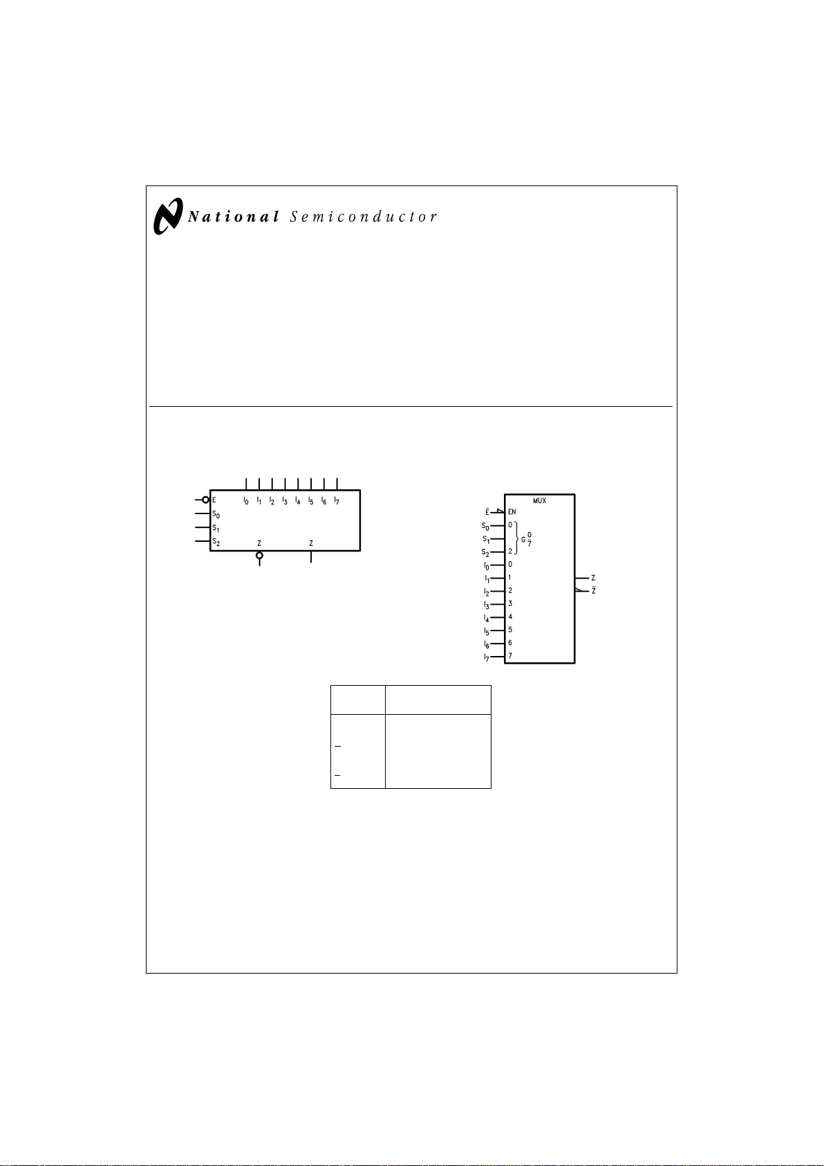
Logic Symbols
Pin
Names
Description
I
0–I7
Data Inputs
S
0–S2
Select Inputs
E
Enable Input
Z Data Output
Z
Inverted Data Output
FACT®is a registered trademark of Fairchild Semiconductor Corporation.
DS100270-1
IEEE/IEC
DS100270-6
August 1998
54AC151
•
54ACT151 8-Input Multiplexer
© 1998 National Semiconductor Corporation DS100270 www.national.com

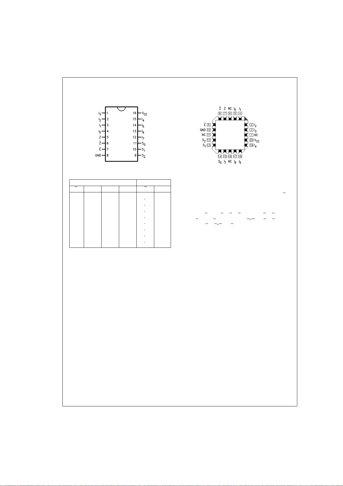
Connection Diagrams
Truth Table
Inputs Outputs
E
S
2
S
1
S
0
Z Z
HXXXHL
LLLLI
0
I
0
LL LHI1I
1
LLHLI2I
2
LLHHI3I
3
LH L L I4I
4
LHLHI5I
5
LHH L I6I
6
LHHHI7I
7
H
=
HIGH Voltage Level
L=LOW Voltage Level
X=Immaterial
Functional Description
The ’AC/’ACT151 is a logic implementation of a single pole,
8-position switch with the switch position controlled by the
state of three Select inputs, S
0,S1,S2
. Both true and
complementary outputs are provided. TheEnable input(E) is
active LOW. When it is not activated, the complementary
output is HIGH and the true output is LOW regardless of all
other inputs. The logic function provided at the output is:
Z=E
•
(I
0
•
S
0
•
S
1
•
S2+I
1
•
S
0
•
S
1
•
S2+
I
2
•
S
0
•
S
1
•
S2+I
3
•
S
0
•
S
1
•
S2+I
4
•
S
0
•
S
1
•
S2+
I
5
•
S
0
•
S
1
•
S2+I
6
•
S
0
•
S
1
•
S2+I
7
•
S
0
•
S
1
•
S2)
The ’AC/’ACT151 provides the ability,in one package to select from eight sources of data or control information. By
proper manipulation of the inputs, the ’AC/’ACT151 can provide any logic function of four variables and its complement.
Pin Assignment
for DIP and Flatpak
DS100270-2
Pin Assignment
for LCC
DS100270-3
www.national.com 2

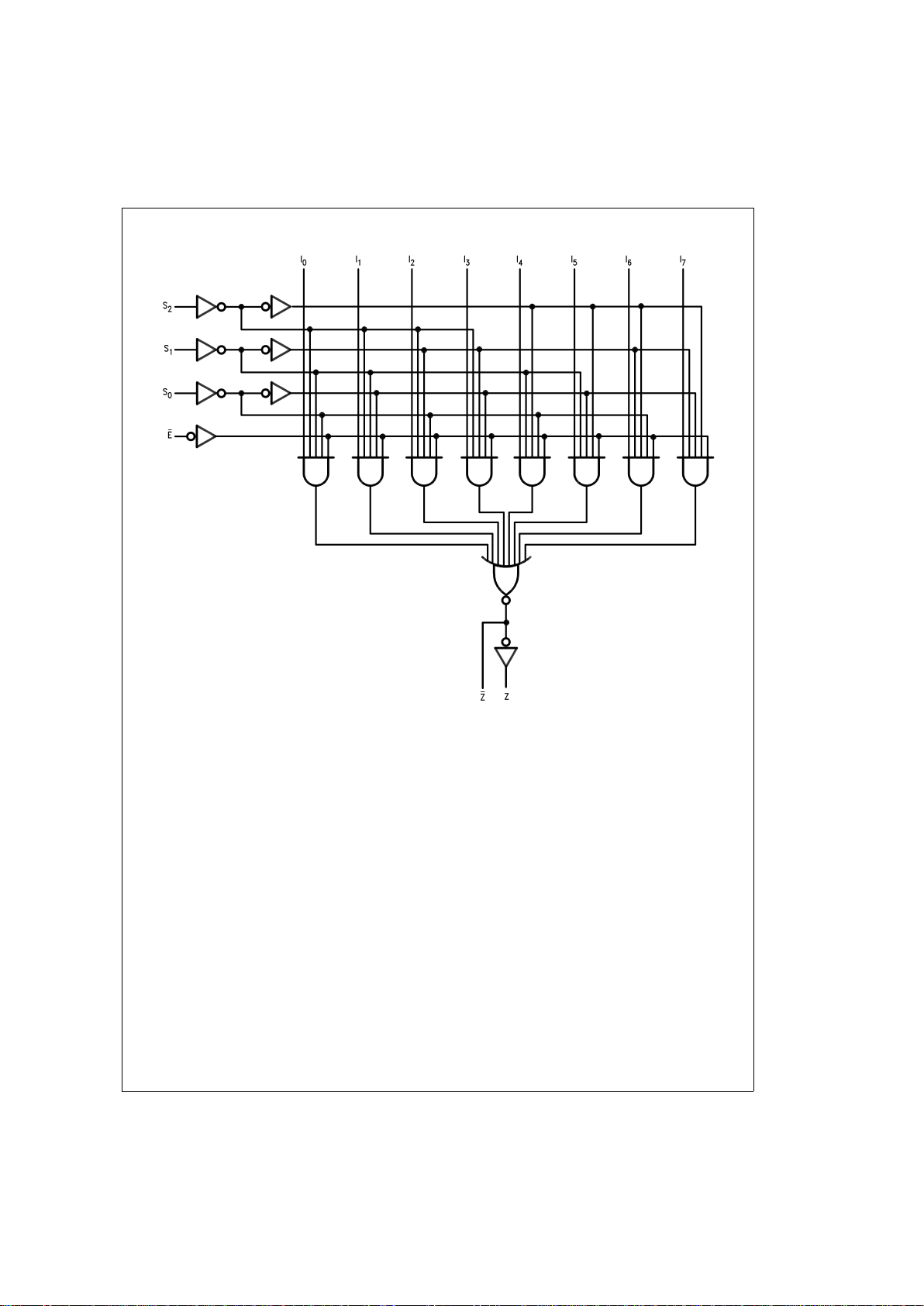
Logic Diagram
DS100270-4
Please note that this diagram is provided only for the understanding of logic operations and should not be used to estimate propagation delays.
3 www.national.com
 Loading...