

Page 1

Customer Care Solutions
Technical Documentation
SERVICE MANUAL
NMP Part No. Issue 1 — 0275709 (RH-40)
09/2003 Issue 2 — 0275789 (RH-42)
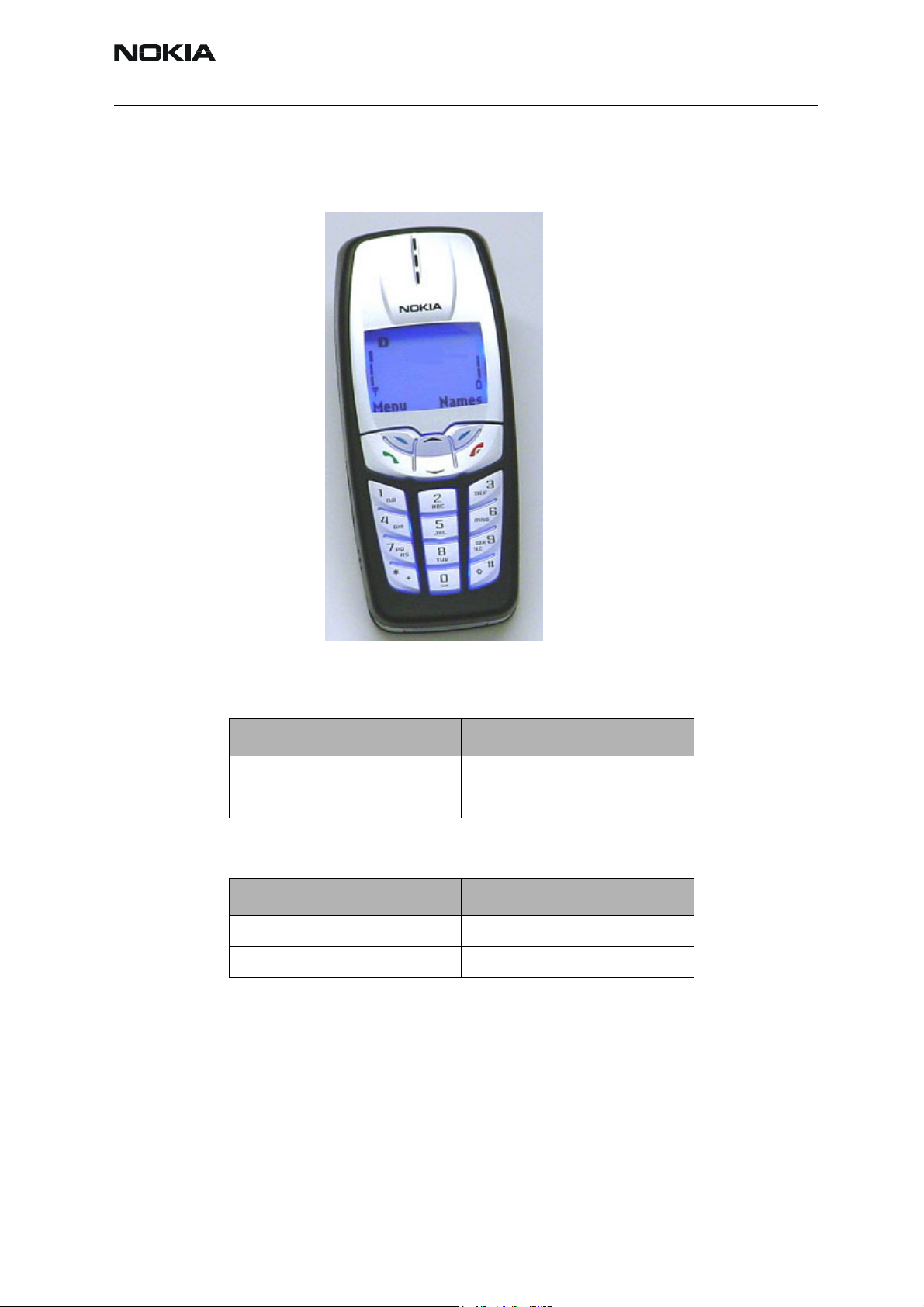
Nokia 2220 (Model RH-42)
Cellular Phones
Issue 2 09/2003 Confidential Copyright 2003 Nokia
Page 2

Customer Care Solutions
Technical Documentation
Amendment Record Sheet
Amendment No Date Inserted By Comments
03/2003 J Fraser Issue 1
Issue 2 09/2003 J Fraser New issue to reflect
change from Safari to
Taco. New parts lists,
new schematics, new
XY-grid information.
Issue 2 09/2003 Confidential Copyright 2003 Nokia
Page 3

Customer Care Solutions
Technical Documentation
RH-42 Series Cellular Phones
Service Manual – Overall Manual Contents
Service Manual comprising
RH-42 Series Transceiver booklet comprising
Foreword
General
Parts
Service Software Instructions
Service Tools
Disassembly/Assembly
Troubleshooting
System Module
Schematics
Issue 2 09/2003 Confidential Copyright 2003 Nokia
Page 4

This document is intended for use by qualified service personnel only.
Company Policy
Our policy is of continuous development; details of all technical modifications will be
included with service bulletins.
While every endeavour has been made to ensure the accuracy of this document, some
errors may exist. If any errors are found by the reader, Nokia Corporation should be notified in writing.
Please state:
Customer Care Solutions
Technical Documentation
IMPORTANT
Title of the Document + Issue Number/Date of publication
Latest Amendment Number (if applicable)
Page(s) and/or Figure(s) in error
Please send to: Nokia Corporation
CCS Technical Documentation
PO Box 86
FIN-24101 SALO
Finland
Issue 2 09/2003 Confidential Copyright 2003 Nokia
Page 5

Customer Care Solutions
Technical Documentation
Warnings and Cautions
Please refer to the phone's user guide for instructions relating to operation, care and
maintenance including important safety information. Note also the following:
Warnings:
1. CARE MUST BE TAKEN ON INSTALLATION IN VEHICLES FITTED WITH
ELECTRONIC ENGINE MANAGEMENT SYSTEMS AND ANTI-SKID BRAKING
SYSTEMS. UNDER CERTAIN FAULT CONDITIONS, EMITTED RF ENERGY CAN
AFFECT THEIR OPERATION. IF NECESSARY, CONSULT THE VEHICLE DEALER/
MANUFACTURER TO DETERMINE THE IMMUNITY OF VEHICLE ELECTRONIC
SYSTEMS TO RF ENERGY.
2. THE HANDPORTABLE TELEPHONE MUST NOT BE OPERATED IN AREAS LIKELY
TO CONTAIN POTENTIALLY EXPLOSIVE ATMOSPHERES EG PETROL STATIONS
(SERVICE STATIONS), BLASTING AREAS ETC.
3. OPERATION OF ANY RADIO TRANSMITTING EQUIPMENT, INCLUDING
Cautions:
1. Servicing and alignment must be undertaken by qualified personnel only.
2. Ensure all work is carried out at an anti-static workstation and that an
3. Ensure solder, wire, or foreign matter does not enter the telephone as
4. Use only approved components as specified in the parts list.
5. Ensure all components, modules screws and insulators are correctly
CELLULAR TELEPHONES, MAY INTERFERE WITH THE FUNCTIONALITY OF
INADEQUATELY PROTECTED MEDICAL DEVICES. CONSULT A PHYSICIAN OR
THE MANUFACTURER OF THE MEDICAL DEVICE IF YOU HAVE ANY
QUESTIONS. OTHER ELECTRONIC EQUIPMENT MAY ALSO BE SUBJECT TO
INTERFERENCE.
anti-static wrist strap is worn.
damage may result.
re-fitted after servicing and alignment. Ensure all cables and wires are
repositioned correctly.
Issue 2 09/2003 Confidential Copyright 2003 Nokia
Page 6

Customer Care Solutions
Technical Documentation
Issue 2 09/2003 Confidential Copyright 2003 Nokia
Page 7

CCS Technical Documentation
RH-42 Series Transceivers
General Information
Issue 2 09/2003 Confidential Nokia Corporation
Page 8

RH-42
General Information CCS Technical Documentation
Page 2 Nokia Corporation Confidential Issue 2 09/2003
Page 9

RH-42
CCS Technical Documentation General Information
Contents
Page No
Product Selection ........................................................................................................... 5
Accessories ..................................................................................................................6
General Specifications of Transceivers RH-42 ...........................................................6
Issue 2 09/2003 Nokia Corporation Confidential Page 3
Page 10

RH-42
General Information CCS Technical Documentation
Page 4 Nokia Corporation Confidential Issue 2 09/2003
Page 11
RH-42
CCS Technical Documentation General Information
Product Selection
The RH-42 (Model 2220) is a single-band handportable mobile telephone for TDMA 800
networks.
Transceiver RH-40 (Model 2220) Phase 1
Unit/type Product Code
Transceiver RH-40 0510337
• radio module 0202138
Transceiver RH-42 (Model 2220) Phase II
Unit/type Product Code
Transceiver RH-42 0510387
• radio module 0202141
Issue 2 09/2003 Nokia Corporation Confidential Page 5
Page 12
RH-42
General Information CCS Technical Documentation
Accessories
Name: Type Code: Material Code:
Transceiver (See Product Variants) See Product Variants
AC Travel Charger ACP-7E
ACP-7U
ACP-7C
ACP-7X
ACP-7H
ACP-7A
Travel Charger (UK plug) 90-264 Vac ACP-8X 0675197
Travel Charger (Made by Nokia)
Travel Charger (China plug) 90-264 Vac
Travel Charger (Australia plug) 90-264 Vac ACP-8A 0675214
Travel Charger ACP-12E
Mobile Charger LCH-9 0675120
Plug-in HF Car Kit PPH-1 0272182
ACP-8U
ACP-8C
ACP-12X
ACP-12U
ACP-12UB
ACP-12G
ACP-12C
ACP-12A
ACP-12AR
0675144
0675143
0675158
0675145
0675146
0675148
0675196
0675211
0675294
0675296
0675303
0675293
0675295
0675297
0675300
0675298
HF Microphone HFM-8 0271503
Headset HDC-5 0694059
Headset HDE-2 0694075
Loopset LPS-3 0630244
Boom Headset HDB-5 0694107
General Specifications of Transceivers RH-42
Table 1: RH-42 General Specifications
Parameter TDMA 800 + AMPS
RX frequency band 869.01 - 893.97 MHz
TX frequency band 824.01 - 848.97 MHz
Output power -5 to +28 dBm/ 0.3 mW to 630 mW
Number of RF channels 832
Channel spacing 30 kHz
0273495
Page 6 Nokia Corporation Confidential Issue 2 09/2003
Page 13

CCS Technical Documentation
RH-42 Series Transceivers
Parts Lists
Issue 2 09/2003 Confidential Nokia Corporation
Page 14

RH-42
Parts Lists CCS Technical Documentation
Page 2 Nokia Corporation Confidential Issue 2 09/2003
Page 15

RH-42
CCS Technical Documentation Parts Lists
Contents
Page No
Exploded View............................................................................................................... 5
Assembly Parts of Basic Transceiver RH-42 ..............................................................5
Component Layout — Top (left) .................................................................................7
Component Layout — Top (right) ...............................................................................7
Component Layout — Bottom ....................................................................................8
Parts Lists....................................................................................................................... 9
RH-42 (2220) — EDMS Issue 4.1 Code: 0202140 (Manaus) ....................................9
RH-42 (2220) — EDMS Issue 3.0 Code: 0202141 (Reynosa) .................................16
Issue 2 09/2003 Nokia Corporation Confidential Page 3
Page 16

RH-42
Parts Lists CCS Technical Documentation
Page 4 Nokia Corporation Confidential Issue 2 09/2003
Page 17
RH-42
CCS Technical Documentation Parts Lists
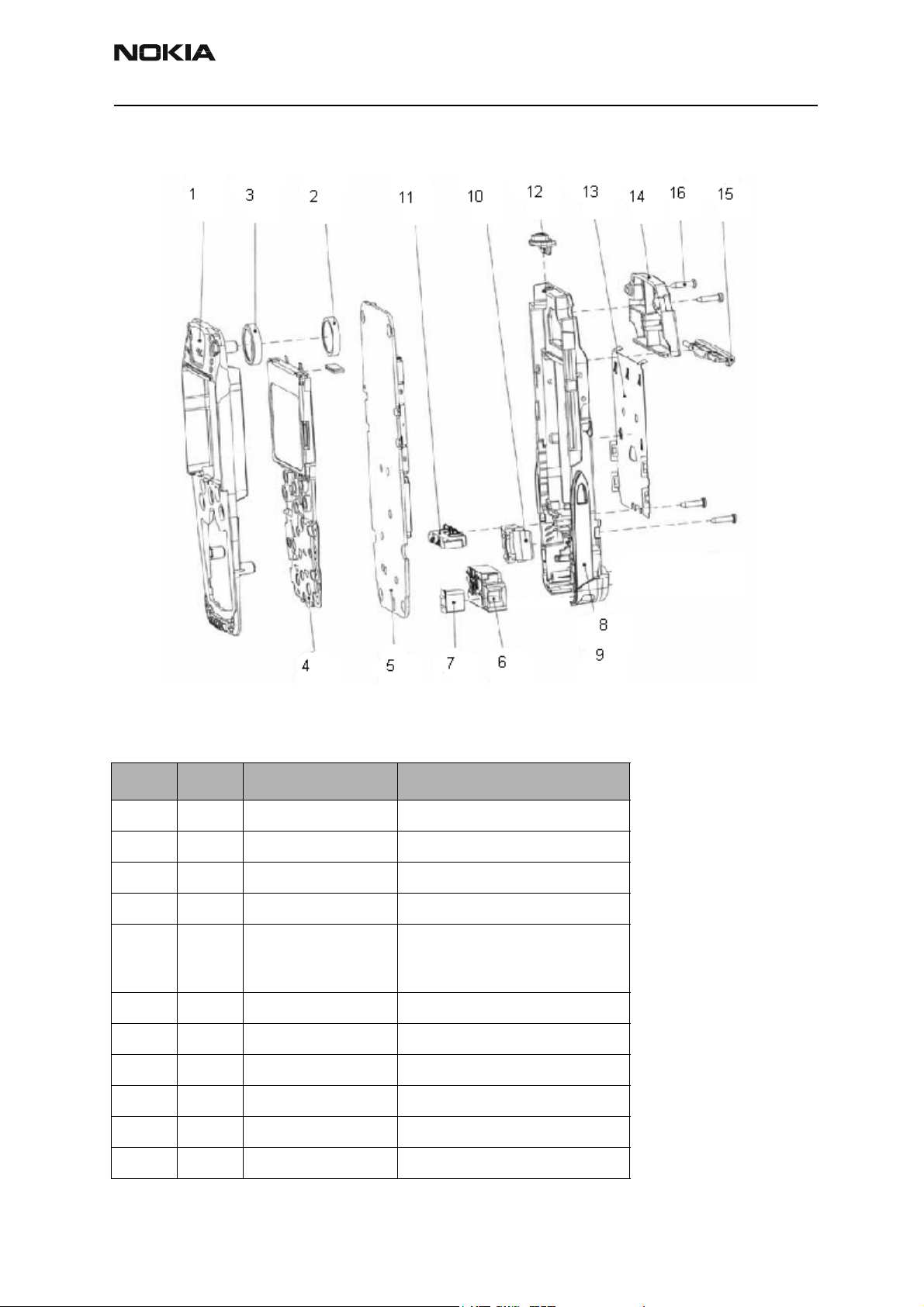
Exploded View
Assembly Parts of Basic Transceiver RH-42
Item Qty Code Description
1 1 9491481 C-cover Assembly
2 1 5140067 Speaker
3 1 9480570 Speaker gasket
4 1 4850139 LCD module Assembly
51
0202141
0202140
1 6800049 Vibra motor Assembly
6 1 5460043 System connector Assembly
7 1 5140201 Microphone Assembly
8 1 9490104 D-cover Assembly
9 1 9451702 D-cover
10 1 5140203 Buzzer Assembly
PWB:
Reynosa
Manaus
Issue 2 09/2003 Nokia Corporation Confidential Page 5
Page 18

RH-42
Parts Lists CCS Technical Documentation
Item Qty Code Description
11 1 5409143 Battery connector
12 1 9451703 Power Button/IR-WINDOW
13 1 9510561 Metal deck
14 1 0660221 Antenna Assembly
15 1 9451706 Battery latch
16 4 6290093 Screws
Page 6 Nokia Corporation Confidential Issue 2 09/2003
Page 19

RH-42
CCS Technical Documentation Parts Lists
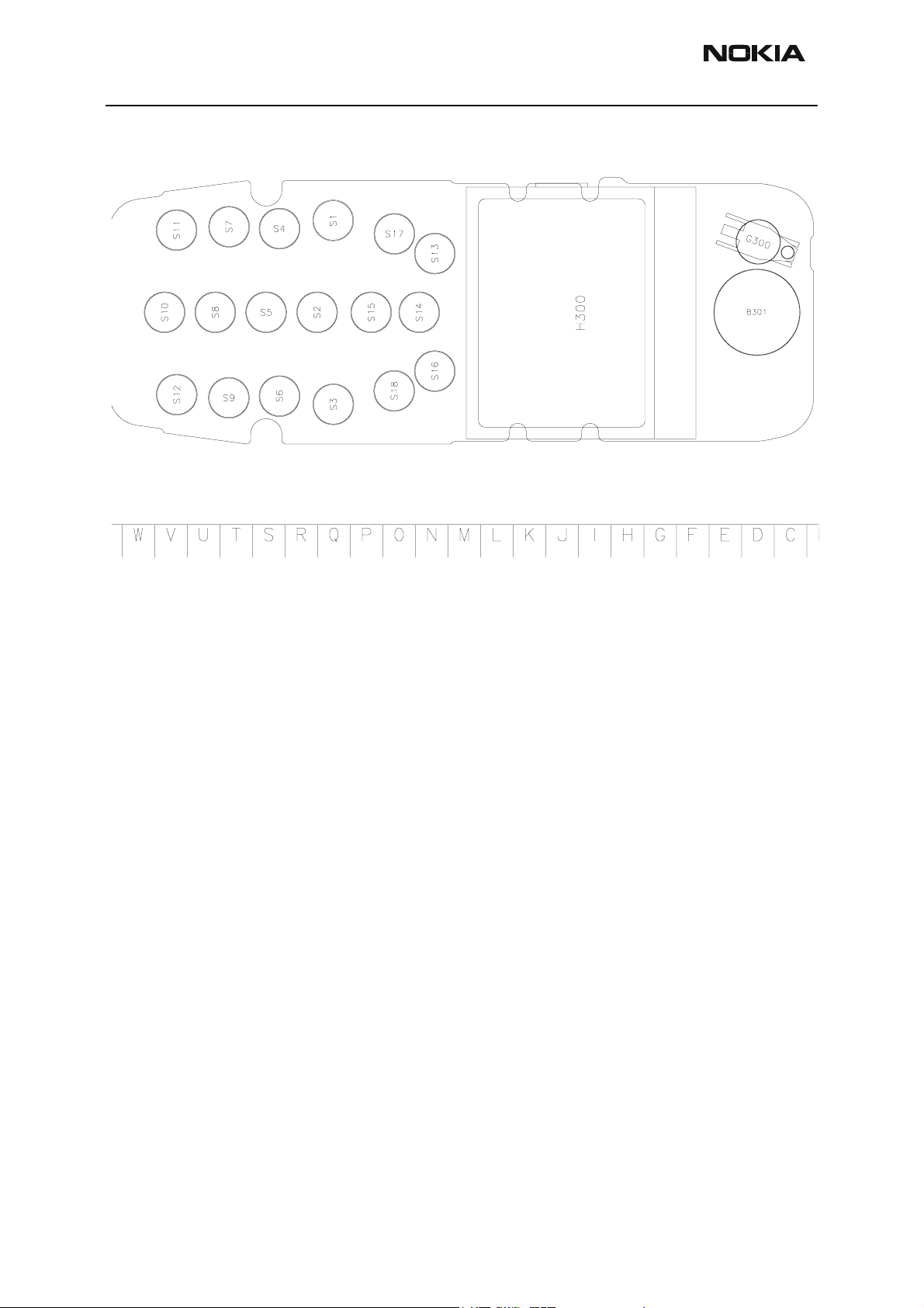
Component Layout — Top (left)
Component Layout — Top (right)
Issue 2 09/2003 Nokia Corporation Confidential Page 7
Page 20
RH-42
Parts Lists CCS Technical Documentation
Component Layout — Bottom
Page 8 Nokia Corporation Confidential Issue 2 09/2003
Page 21

RH-42
CCS Technical Documentation Parts Lists
Parts Lists
RH-42 (2220) — EDMS Issue 4.1 Code: 0202140 (Manaus)
Item Code Side X Y Description Value Type
R100 1825133 Top R 6 var chip 14V/50V 0402
R101 1825133 Top U 7 var chip 14V/50V 0402
R102 1825133 Top U 7 var chip 14V/50V 0402
R150 1620031 Top R 9 res network 0W06 2X1K0 J 0404
R151 1430778 Top S 9 chip res 0W06 10K J 0402
R152 1430788 Top R 9 chip res 0W06 22K J 0402
R156 1430762 Top V 5 chip res 0W06 2K2 J 0402
R157 1430710 Top R 11 chip res 0W06 22R J 0402
R200 1414605 Top S 10 chip res 0W25 0R22 J 0805
R201 1620103 Top T 10 res network 0W06 2X22R J 0404
R202 1620043 Top R 7 chip res 0W06 100K J 0402
R203 1430804 Top R 7 chip res 0W06 100K J 0603
R206 1430770 Top Q 7 chip res 0W06 100K J 0402
R207 1430770 Top Q 7 chip res 0W06 100K J 0402
R208 1430804 Top R 7 resistor 100k 0402
R300 1411669 Top T 9 chip res 0W1 22R J 0805
R301 1413829 Top P 6 chip res 0W1 10R J 0805
R420 1430268 Top O 8 chip res 0W06 27K F
100PPM
R427 1430778 Top N 7 chip res 0W06 10K J 0402
R450 1430770 Top O 6 chip res 0W06 4K7 J 0402
R709 1430700 Top K 9 chip res 0W06 10R J 0402
R712 1430700 Top J 10 chip res 0W06 10R J 0402
0603
R721 1430796 Top J 9 chip res 0W06 6K8 J 0402
R741 1430796 Top K 10 chip res 0W06 4K7 J 0402
R771 1430786 Top M 6 chip res 0W06 18K J 0402
R772 1430726 Top M 7 chip res 0W06 100R J 0402
R773 1430700 Top M 7 chip res 0W06 10R J 0402
R774 1430700 Top k 7 chip res 0W06 10R J 0402
R791 1430778 Top M 9 chip res 0W06 10K J 0402
Issue 2 09/2003 Nokia Corporation Confidential Page 9
Page 22

RH-42
Parts Lists CCS Technical Documentation
Item Code Side X Y Description Value Type
R792 1430700 Top M 9 chip res 0W06 10R J 0402
R818 1430268 Top H 7 chip res 0W06 27K F
100PPM
R820 1430740 Top I 7 resistor 330R 0402
R830 1430832 Top M 8 chip res 0W06 2K7 J 0402
R831 1430734 Top J 8 chip res 0W06 220R J 0402
C101 2320536 Top R 8 chip cap NP0 10P J 50V 0402
C102 2320756 Top U 8 chip cap X7R 3N3 K 50V 0402
C103 2320756 Top U 7 chip cap X7R 3N3 K 50V 0402
C104 2320756 Top U 7 chip cap X7R 3N3 K 50V 0402
C105 2320756 Top U 7 chip cap X7R 3N3 K 50V 0402
C106 2320744 Top T 8 chip cap X7R 1N0 K 50V 0402
C150 2312243 Top U 10 chip cap X5R 4U7 K 6V3 0805
C151 2320783 Top V 5 chip cap X7R 33N K 10V 0402
C152 2320783 Top V 5 chip cap X7R 33N K 10V 0402
C155 2320783 Top R 9 chip cap X7R 33N K 10V 0402
0603
C156 2320783 Top R 9 chip cap X7R 33N K 10V 0402
C157 2320560 Top R 9 chip cap NP0 100P J 50V 0402
C159 2320560 Top R 9 chip cap NP0 100P J 50V 0402
C160 2320744 Top S 9 chip cap X7R 1N0 K 50V 0402
C161 2320481 Top S 9 chip cap X5R 1U K 6V3 0603
C200 2320805 Top P 10 chip cap 100N 10V 0402
C201 2320481 Top O 10 chip cap X5R 1U K 6V3 0603
C202 2320778 Top S 10 chip cap NP0 33P J 50V 0402
C205 2320481 Top P 10 chip cap X5R 1U K 6V3 0603
C206 2320481 Top Q 10 chip cap X5R 1U K 6V3 0603
C207 2320481 Top R 8 chip cap X5R 1U K 6V3 0603
C208 2320481 Top O 10 chip cap X5R 1U K 6V3 0603
C209 2320536 Top R 11 chip cap 10P 50V 0402
C210 2320536 Top R 9 chip cap 10P 50V 0402
C211 2320481 Top Q 10 chip cap X5R 1U K 6V3 0603
C212 2320481 Top Q 10 chip cap X5R 1U K 6V3 0603
C213 2320481 Top Q 10 chip cap X5R 1U K 6V3 0603
Page 10 Nokia Corporation Confidential Issue 2 09/2003
Page 23
RH-42
CCS Technical Documentation Parts Lists
Item Code Side X Y Description Value Type
C214 2320481 Top N 10 chip cap 1U0 6.3V 0603
C215 2320481 Top R 8 chip cap X5R 1U K 6V3 0603
C218 2320805 Top P 7 chip cap X5R 100N K 10V 0402
C219 2320139 Top O 10 chip cap X5R 1U0 K 10V 0603
C220 2320778 Top Q 7 chip cap X7R 1N0 K 50V 0402
C221 2320481 Top O 10 chip cap X5R 1U0 6.3V 0603
C222 2320481 Top N 10 chip cap X5R 1U0 6.3V 0603
C223 2320481 Top O 9 chip cap X5R 1U0 6.3V 0603
C224 2320481 Top N 9 chip cap X5R 1U0 6.3V 0603
C226 2320481 Top N 8 chip cap X5R 1U0 6.3V 0603
C227 2320481 Top N 9 chip cap 1U0 6.3V 0603
C228 2320481 Top O 8 chip cap X5R 1U0 6.3V 0603
C229 2320481 Top O 8 chip cap X5R 1U0 6.3V 0603
C230 2320481 Top O 10 chip cap X5R 1U0 6.3V 0603
C231 2320481 Top O 8 chip cap X5R 1U0 6.3V 0603
C232 2320481 Top O 9 chip cap X5R 1U0 6.3V 0603
C234 2320481 Top O 9 chip cap X5R 1U0 6.3V 0603
C235 2320481 Top R 8 chip cap X5R 1U0 6.3V 0603
C236 2320805 Top O 7 chip cap X5R 100N K 10V 0402
C237 2320805 Top O 7 chip cap X5R 100N K 10V 0402
C238 2320805 Top P 10 chip cap X7R 220N K 10V 0603
C239 2320805 Top Q 7 chip cap X5R 100N K 10V 0402
C240 2320778 Top Q 7 chip cap 10N 16V 0402
C241 2320744 Top Q 7 chip cap NP0 22P J 50V 0402
C242 2320744 Top Q 7 chip cap NP0 22P J 50V 0402
C243 2320481 Top N 9 chip cap 1U0 6.3V 0603
C244 2320544 Top R 9 chip cap 22P 50V 0402
C245 2320544 Top R 9 chip cap 22P 50V 0402
C260 2312249 Top P 10 chip cap 4U7 10V 0805
C261 2312249 Top O 9 chip cap X5R 4U7 K 6V3 0805
C264 2320139 Top R 7 chip cap X5R 1U K 6V3 0603
C302 2320779 Top D 5 chip cap X7R 100N K 16V 0603
Issue 2 09/2003 Nokia Corporation Confidential Page 11
Page 24

RH-42
Parts Lists CCS Technical Documentation
Item Code Side X Y Description Value Type
C303 2320805 Top E 5 chip cap X5R 100N K 10V 0402
C304 2320805 Top E 5 chip cap X5R 100N K 10V 0402
C306 2320560 Top V 10 chip cap NP0 100P J 50V 0402
C307 2320548 Top V 5 chip cap 33P 50V 0402
C308 2320560 Top V 5 chip cap 100P 50V 0402
C400 2320778 Top R 6 chip cap X7R 10N K 16V 0402
C401 2320805 Top R 6 chip cap X5R 100N K 10V 0402
C402 2320778 Top P 6 chip cap X7R 10N K 16V 0402
C403 2320778 Top P 6 chip cap X7R 10N K 16V 0402
C404 2320778 Top Q 6 chip cap X7R 10N K 16V 0402
C405 2320778 Top O 6 chip cap X7R 10N K 16V 0402
C420 2320744 Top O 6 chip cap X7R 1N0 K 50V 0402
C450 2320778 Top O 6 chip cap X7R 10N K 16V 0402
C451 2320805 Top O 6 chip cap X5R 100N K 10V 0402
C454 2320779 Top N 6 chip cap X7R 100N K 16V 0603
C700 2320552 Top H 8 chip cap NP0 47P J 50V 0402
C701 2320536 Top I 8 chip cap NP0 10P J 50V 0402
C702 2320805 Top H 8 chip cap X5R 100N K 10V 0402
C703 2320536 Top I 8 chip cap NP0 10P J 50V 0402
C704 2320805 Top H 8 chip cap X5R 100N K 10V 0402
C706 2320552 Top K 9 chip cap NP0 47P J 50V 0402
C707 2320744 Top K 9 chip cap X7R 1N0 K 50V 0402
C708 2320481 Top K 9 chip cap X5R 1U K 6V3 0603
C710 2320740 Top I 9 chip cap X7R 680P K 50V 0402
C711 2320481 Top J 10 chip cap X5R 1U K 6V3 0603
C712 2320552 Top K 9 chip cap NP0 47P J 50V 0402
C720 2320564 Top J 9 chip cap X7R 1N5 J 50V 0402
C721 2322023 Top J 9 chip cap X7R 33N K 10V 0402
C740 2320564 Top K 9 chip cap X7R 1N8 J 50V 0402
C741 2322023 Top K 10 chip cap X7R 33N K 10V 0402
C770 2320580 Top M 6 chip cap X7R 680P J 50V 0402
C771 2480003 Top M 6 chip cap PPS 8N2 J 16V 0805
Page 12 Nokia Corporation Confidential Issue 2 09/2003
Page 25

RH-42
CCS Technical Documentation Parts Lists
Item Code Side X Y Description Value Type
C772 2320495 Top M 6 chip cap NP0 1N0 J 50V 0603
C773 2320466 Top M 7 chip cap NP0 220P J 60V 0603
C774 2320536 Top K 7 chip cap NP0 10P J 50V 0402
C775 2320481 Top K 7 chip cap X5R 1U K 6V3 0603
C776 2320778 Top K 7 chip cap X7R 10N K 16V 0402
C777 2320536 Top J 6 chip cap 10P 50V 0402
C778 2320536 Top J 6 chip cap 10P 50V 0402
C791 2320805 Top M 9 chip cap X5R 100N K 10V 0402
C792 2320778 Top L 9 chip cap X7R 10N K 16V 0402
C793 2320481 Top L 9 chip cap X5R 1U K 6V3 0603
C801 2320552 Top I 7 chip cap NP0 47P J 50V 0402
C802 2320778 Top I 7 chip cap X7R 10N K 16V 0402
C803 2320536 Top I 7 chip cap NP0 10P J 50V 0402
C806 2320552 Top K 8 chip cap NP0 47P J 50V 0402
C807 2320536 Top J 8 chip cap NP0 10P J 50V 0402
C808 2320805 Top K 9 chip cap X5R 100N K 10V 0402
C820 2320552 Top J 7 chip cap NP0 47P J 50V 0402
C821 2320552 Top J 7 chip cap NP0 47P J 50V 0402
C822 2320805 Top K 7 chip cap X5R 100N K 10V 0402
C830 2320778 Top M 8 chip cap X7R 10N K 16V 0402
C831 2320602 Top M 8 chip cap NP0 4P7 C 50V 0402
C832 2320602 Top M 8 chip cap NP0 4P7 C 50V 0402
C833 2320536 Top K 8 chip cap NP0 10P J 50V 0402
C834 2320536 Top K 8 chip cap NP0 10P J 50V 0402
C910 2320744 Top H 4 chip cap X7R 1N0 K 50V 0402
C911 2320778 Top I 5 chip cap X7R 10N K 16V 0402
C913 2320560 Top J 5 chip cap 100P 50V 0402
C914 2320481 Top J 5 chip cap X5R 1U K 6V3 0603
C915 2320536 Top I 9 chip cap NP0 10P J 50V 0402
C916 2320805 Top H 9 chip cap X5R 100N K 10V 0402
C919 2320508 Top H 5 chip cap 1P0 50V 0402
C923 2320604 Top H 9 chip cap 18P 50V 0402
Issue 2 09/2003 Nokia Corporation Confidential Page 13
Page 26
RH-42
Parts Lists CCS Technical Documentation
Item Code Side X Y Description Value Type
C924 2320604 Top J 4 chip cap 18P 50V 0402
C930 2320536 Top G 7 chip cap NP0 10P J 50V 0402
C931 2320744 Top G 6 chip cap X7R 1N0 K 50V 0402
C960 2320536 Top I 10 chip cap NP0 1P0 C 50V 0402
C961 2320536 Top I 10 chip cap NP0 2P7 C 50V 0402
C971 2320536 Top I 9 chip cap NP0 10P J 50V 0402
C972 2320805 Top J 9 chip cap X5R 100N K 10V 0402
C975 2320560 Top J 10 chip cap 100P 50V 0402
L100 3203743 Top U 7 ferrite bead 0R03 42R/100MHz 3A0805
L160 3203741 Top U 7 ferrite bead 0R5 600R/100MHz 0603
L161 3203741 Top U 7 ferrite bead 0R5 600R/100MHz 0603
L162 3203741 Top U 7 ferrite bead 0R5 600R/100MHz 0603
L163 3203741 Top U 6 ferrite bead 0R5 600R/100MHz 0603
L164 3203741 Top V 5 ferrite bead 0R5 600R/100MHz 0603
L730 3645093 Top K 9 chip coil 36 N G Q55/500MHz 0603
L746 3645091 Top J 9 chip coil 22N G Q55/500MHz 0603
L820 3645211 Top J 7 chip coil 6N8 K Q27/250MHz 0603
L821 3646069 Top J 7 chip coil 33N J Q23/800MHz 0402
L822 3646063 Top J 7 chip coil 22N J Q28/800MHz 0402
L830 3643087 Top M 7 chip coil 180N J Q13/50MHz 0805
L831 3643087 Top M 8 chip coil 180N J Q13/50MHz 0805
L832 3645067 Top K 8 chip coil 330N J Q48/250MHz 0805
L903 3643085 Top I 5 chip coil 5N6+-0N5 Q35 1.5A 0805
L960 3646083 Top I 10 chip coil 100N J Q16/300MHz 0402
L961 3646083 Top I 10 chip coil 100N J Q16/300MHz 0402
L962 3646083 Top H 10 chip coil 100N J Q16/300MHz 0402
L963 3646083 Top H 10 chip coil 100N J Q16/300MHz 0402
V100 4110028 Top T 8 TVS DI 16V 600W 23A DO214AA
V300 4860221 Top K 11 LED M47CN2Q135 Blue >45 MCD TOPLED
V301 4860221 Top I 11 LED M47CN2Q135 Blue >45 MCD TOPLED
V302 4860221 Top K 3 LED M47CN2Q135 Blue >45 MCD TOPLED
V303 4860221 Top I 3 LED M47CN2Q135 Blue >45 MCD TOPLED
Page 14 Nokia Corporation Confidential Issue 2 09/2003
Page 27

RH-42
CCS Technical Documentation Parts Lists
Item Code Side X Y Description Value Type
V304 4860221 Top N 6 LED M47CN2Q135 Blue >45 MCD TOPLED
V305 4860221 Top S 9 LED M47CN2Q135 Blue >45 MCD TOPLED
V306 4860221 Top U 6 LED M47CN2Q135 Blue >45 MCD TOPLED
V308 4860221 Top Q 6 LED M47CN2Q135 Blue >45 MCD TOPLED
V309 4860221 Top N 8 LED M47CN2Q135 Blue >45 MCD TOPLED
N801 4370915 Top I 8 Taco 3.1 TZC8CRTT TFBGA108
N901 4350401 Top I 5 Pw Amp RF9270 TDMA
N930 4350407 Top G 6 Pwr Detector Module 800MHz 2.7V
D200 4370825 Top P 9 UEMK W-DOG ENA TO21 TFBGA168
D400 4370811 Top Q 5 UPP V2.4 F741809C C05 ANAM UBG
D450 4341439 Top O 5 Flash 1MX16 1.8V/1.8V TFGBA48
G780 4350279 Top L 6 VCO 2GHz 2.78V 10.5MA TDMA
G790 4510307 Top M 10 VCTCXO 19.44MHz+- 2.5PPM 2.78V
B200 4510303 Top R 10 Crystal 32.768KHz+- 20PPM 12.5PF
Z301 4120031 Top V 4 EMI/ESD Filt EMIF10-
1K010F1
Z820 4510357 Top J 6 Saw Filt 881.5+-
12.5MHz/
Z830 4511351 Top L 8 Saw Filt 135.54+- 0.013MHz/ 6X3.5MM
Z905 4511357 Top J 4 Saw Filt 836.5+- 12.5MHz/3.0 2.5X2
Z906 4512173 Top G 5 Dupl 824-849/ 869-894MHz 5X5X1.7
Z907 4550117 Top D 6 Dipl 824-894/1850- 1990MHz 3.2X1.6
Z960 4511353 Top I 10 Saw Filt 180.54+- 0.015MHz 3X3MM
T775 4550153 Top K 6 Transf Balun 2060+- 70MHz 2.0X1.25
T961 4550247 Top I 9 Transf Balun 1:4 836MHz 1.8X3.4
F100 5119019 Top U 8 Sm Fuse F 1.5A 32V 0603
S300 5209001 Top C 9 Sm SW Tact SPST 12V 50MA Side Key
3DB 2.5X2
BGA24
X900 5429021 Top C 5 Sm Conn RF+SW 100V 1W 50R 2.2GHz
A100 9510612 Top P 7 Baseband Shield DMD06548 HDA62_72
A900 9517071 Top J 7 RF Shield Assy DMC02311 HDA62_72
Issue 2 09/2003 Nokia Corporation Confidential Page 15
Page 28

RH-42
Parts Lists CCS Technical Documentation
RH-42 (2220) — EDMS Issue 3.0 Code: 0202141 (Reynosa)
Item Code Side X Y Description Value Type
R100 1825133 Top R 6 var chip 14V/50V 0402
R101 1825133 Top U 7 var chip 14V/50V 0402
R102 1825133 Top U 7 var chip 14V/50V 0402
R150 1620031 Top R 9 res network 0W06 2X1K0 J 0404
R151 1430778 Top S 9 chip res 0W06 10K J 0402
R152 1430788 Top R 9 chip res 0W06 22K J 0402
R156 1430762 Top V 5 chip res 0W06 2K2 J 0402
R157 1430710 Top R 11 chip res 0W06 22R J 0402
R200 1414605 Top S 10 chip res 0W25 0R22 J 0805
R201 1620103 Top T 10 res network 0W06 2X22R J 0404
R202 1620043 Top R 7 chip res 0W06 100K J 0402
R203 1430804 Top R 7 chip res 0W06 100K J 0603
R206 1430770 Top Q 7 chip res 0W06 100K J 0402
R207 1430770 Top Q 7 chip res 0W06 100K J 0402
R208 1430804 Top R 7 resistor 100k 0402
R300 1411669 Top T 9 chip res 0W1 22R J 0805
R301 1413829 Top P 6 chip res 0W1 10R J 0805
R420 1430268 Top O 8 chip res 0W06 27K F
100PPM
R427 1430778 Top N 7 chip res 0W06 10K J 0402
R450 1430770 Top O 6 chip res 0W06 4K7 J 0402
R709 1430700 Top K 9 chip res 0W06 10R J 0402
R712 1430700 Top J 10 chip res 0W06 10R J 0402
R721 1430796 Top J 9 chip res 0W06 6K8 J 0402
R741 1430796 Top K 10 chip res 0W06 4K7 J 0402
0603
R771 1430786 Top M 6 chip res 0W06 18K J 0402
R772 1430726 Top M 7 chip res 0W06 100R J 0402
R773 1430700 Top M 7 chip res 0W06 10R J 0402
R774 1430700 Top k 7 chip res 0W06 10R J 0402
R791 1430778 Top M 9 chip res 0W06 10K J 0402
R792 1430700 Top M 9 chip res 0W06 10R J 0402
Page 16 Nokia Corporation Confidential Issue 2 09/2003
Page 29

RH-42
CCS Technical Documentation Parts Lists
Item Code Side X Y Description Value Type
R818 1430268 Top H 7 chip res 0W06 27K F
100PPM
R820 1430740 Top I 7 resistor 330R 0402
R830 1430832 Top M 8 chip res 0W06 2K7 J 0402
R831 1430734 Top J 8 chip res 0W06 220R J 0402
C101 2320536 Top R 8 chip cap NP0 10P J 50V 0402
C102 2320756 Top U 8 chip cap X7R 3N3 K 50V 0402
C103 2320756 Top U 7 chip cap X7R 3N3 K 50V 0402
C104 2320756 Top U 7 chip cap X7R 3N3 K 50V 0402
C105 2320756 Top U 7 chip cap X7R 3N3 K 50V 0402
C106 2320744 Top T 8 chip cap X7R 1N0 K 50V 0402
C150 2312243 Top U 10 chip cap X5R 4U7 K 6V3 0805
C151 2320783 Top V 5 chip cap X7R 33N K 10V 0402
C152 2320783 Top V 5 chip cap X7R 33N K 10V 0402
C155 2320783 Top R 9 chip cap X7R 33N K 10V 0402
0603
C156 2320783 Top R 9 chip cap X7R 33N K 10V 0402
C157 2320560 Top R 9 chip cap NP0 100P J 50V 0402
C159 2320560 Top R 9 chip cap NP0 100P J 50V 0402
C160 2320744 Top S 9 chip cap X7R 1N0 K 50V 0402
C161 2320481 Top S 9 chip cap X5R 1U K 6V3 0603
C200 2320805 Top P 10 chip cap 100N 10V 0402
C201 2320481 Top O 10 chip cap X5R 1U K 6V3 0603
C202 2320778 Top S 10 chip cap NP0 33P J 50V 0402
C205 2320481 Top P 10 chip cap X5R 1U K 6V3 0603
C206 2320481 Top Q 10 chip cap X5R 1U K 6V3 0603
C207 2320481 Top R 8 chip cap X5R 1U K 6V3 0603
C208 2320481 Top O 10 chip cap X5R 1U K 6V3 0603
C209 2320536 Top R 11 chip cap 10P 50V 0402
C210 2320536 Top R 9 chip cap 10P 50V 0402
C211 2320481 Top Q 10 chip cap X5R 1U K 6V3 0603
C212 2320481 Top Q 10 chip cap X5R 1U K 6V3 0603
C213 2320481 Top Q 10 chip cap X5R 1U K 6V3 0603
C214 2320481 Top N 10 chip cap 1U0 6.3V 0603
Issue 2 09/2003 Nokia Corporation Confidential Page 17
Page 30

RH-42
Parts Lists CCS Technical Documentation
Item Code Side X Y Description Value Type
C215 2320481 Top R 8 chip cap X5R 1U K 6V3 0603
C218 2320805 Top P 7 chip cap X5R 100N K 10V 0402
C219 2320139 Top O 10 chip cap X5R 1U0 K 10V 0603
C220 2320778 Top Q 7 chip cap X7R 1N0 K 50V 0402
C221 2320481 Top O 10 chip cap X5R 1U0 6.3V 0603
C222 2320481 Top N 10 chip cap X5R 1U0 6.3V 0603
C223 2320481 Top O 9 chip cap X5R 1U0 6.3V 0603
C224 2320481 Top N 9 chip cap X5R 1U0 6.3V 0603
C226 2320481 Top N 8 chip cap X5R 1U0 6.3V 0603
C227 2320481 Top N 9 chip cap 1U0 6.3V 0603
C228 2320481 Top O 8 chip cap X5R 1U0 6.3V 0603
C229 2320481 Top O 8 chip cap X5R 1U0 6.3V 0603
C230 2320481 Top O 10 chip cap X5R 1U0 6.3V 0603
C231 2320481 Top O 8 chip cap X5R 1U0 6.3V 0603
C232 2320481 Top O 9 chip cap X5R 1U0 6.3V 0603
C234 2320481 Top O 9 chip cap X5R 1U0 6.3V 0603
C235 2320481 Top R 8 chip cap X5R 1U0 6.3V 0603
C236 2320805 Top O 7 chip cap X5R 100N K 10V 0402
C237 2320805 Top O 7 chip cap X5R 100N K 10V 0402
C238 2320805 Top P 10 chip cap X7R 220N K 10V 0603
C239 2320805 Top Q 7 chip cap X5R 100N K 10V 0402
C240 2320778 Top Q 7 chip cap 10N 16V 0402
C241 2320744 Top Q 7 chip cap NP0 22P J 50V 0402
C242 2320744 Top Q 7 chip cap NP0 22P J 50V 0402
C243 2320481 Top N 9 chip cap 1U0 6.3V 0603
C244 2320544 Top R 9 chip cap 22P 50V 0402
C245 2320544 Top R 9 chip cap 22P 50V 0402
C260 2312249 Top P 10 chip cap 4U7 10V 0805
C261 2312249 Top O 9 chip cap X5R 4U7 K 6V3 0805
C264 2320139 Top R 7 chip cap X5R 1U K 6V3 0603
C302 2320779 Top D 5 chip cap X7R 100N K 16V 0603
C303 2320805 Top E 5 chip cap X5R 100N K 10V 0402
Page 18 Nokia Corporation Confidential Issue 2 09/2003
Page 31

RH-42
CCS Technical Documentation Parts Lists
Item Code Side X Y Description Value Type
C304 2320805 Top E 5 chip cap X5R 100N K 10V 0402
C306 2320560 Top V 10 chip cap NP0 100P J 50V 0402
C307 2320548 Top V 5 chip cap 33P 50V 0402
C308 2320560 Top V 5 chip cap 100P 50V 0402
C400 2320778 Top R 6 chip cap X7R 10N K 16V 0402
C401 2320805 Top R 6 chip cap X5R 100N K 10V 0402
C402 2320778 Top P 6 chip cap X7R 10N K 16V 0402
C403 2320778 Top P 6 chip cap X7R 10N K 16V 0402
C404 2320778 Top Q 6 chip cap X7R 10N K 16V 0402
C405 2320778 Top O 6 chip cap X7R 10N K 16V 0402
C420 2320744 Top O 6 chip cap X7R 1N0 K 50V 0402
C450 2320778 Top O 6 chip cap X7R 10N K 16V 0402
C451 2320805 Top O 6 chip cap X5R 100N K 10V 0402
C454 2320779 Top N 6 chip cap X7R 100N K 16V 0603
C700 2320552 Top H 8 chip cap NP0 47P J 50V 0402
C701 2320536 Top I 8 chip cap NP0 10P J 50V 0402
C702 2320805 Top H 8 chip cap X5R 100N K 10V 0402
C703 2320536 Top I 8 chip cap NP0 10P J 50V 0402
C704 2320805 Top H 8 chip cap X5R 100N K 10V 0402
C706 2320552 Top K 9 chip cap NP0 47P J 50V 0402
C707 2320744 Top K 9 chip cap X7R 1N0 K 50V 0402
C708 2320481 Top K 9 chip cap X5R 1U K 6V3 0603
C710 2320740 Top I 9 chip cap X7R 680P K 50V 0402
C711 2320481 Top J 10 chip cap X5R 1U K 6V3 0603
C712 2320552 Top K 9 chip cap NP0 47P J 50V 0402
C720 2320564 Top J 9 chip cap X7R 1N5 J 50V 0402
C721 2322023 Top J 9 chip cap X7R 33N K 10V 0402
C740 2320564 Top K 9 chip cap X7R 1N8 J 50V 0402
C741 2322023 Top K 10 chip cap X7R 33N K 10V 0402
C770 2320580 Top M 6 chip cap X7R 680P J 50V 0402
C771 2480003 Top M 6 chip cap PPS 8N2 J 16V 0805
C772 2320495 Top M 6 chip cap NP0 1N0 J 50V 0603
Issue 2 09/2003 Nokia Corporation Confidential Page 19
Page 32

RH-42
Parts Lists CCS Technical Documentation
Item Code Side X Y Description Value Type
C773 2320466 Top M 7 chip cap NP0 220P J 60V 0603
C774 2320536 Top K 7 chip cap NP0 10P J 50V 0402
C775 2320481 Top K 7 chip cap X5R 1U K 6V3 0603
C776 2320778 Top K 7 chip cap X7R 10N K 16V 0402
C777 2320536 Top J 6 chip cap 10P 50V 0402
C778 2320536 Top J 6 chip cap 10P 50V 0402
C791 2320805 Top M 9 chip cap X5R 100N K 10V 0402
C792 2320778 Top L 9 chip cap X7R 10N K 16V 0402
C793 2320481 Top L 9 chip cap X5R 1U K 6V3 0603
C801 2320552 Top I 7 chip cap NP0 47P J 50V 0402
C802 2320778 Top I 7 chip cap X7R 10N K 16V 0402
C803 2320536 Top I 7 chip cap NP0 10P J 50V 0402
C806 2320552 Top K 8 chip cap NP0 47P J 50V 0402
C807 2320536 Top J 8 chip cap NP0 10P J 50V 0402
C808 2320805 Top K 9 chip cap X5R 100N K 10V 0402
C820 2320552 Top J 7 chip cap NP0 47P J 50V 0402
C821 2320552 Top J 7 chip cap NP0 47P J 50V 0402
C822 2320805 Top K 7 chip cap X5R 100N K 10V 0402
C830 2320778 Top M 8 chip cap X7R 10N K 16V 0402
C831 2320602 Top M 8 chip cap NP0 4P7 C 50V 0402
C832 2320602 Top M 8 chip cap NP0 4P7 C 50V 0402
C833 2320536 Top K 8 chip cap NP0 10P J 50V 0402
C834 2320536 Top K 8 chip cap NP0 10P J 50V 0402
C910 2320744 Top H 4 chip cap X7R 1N0 K 50V 0402
C911 2320778 Top I 5 chip cap X7R 10N K 16V 0402
C913 2320560 Top J 5 chip cap 100P 50V 0402
C914 2320481 Top J 5 chip cap X5R 1U K 6V3 0603
C915 2320536 Top I 9 chip cap NP0 10P J 50V 0402
C916 2320805 Top H 9 chip cap X5R 100N K 10V 0402
C919 2320508 Top H 5 chip cap 1P0 50V 0402
C923 2320604 Top H 9 chip cap 18P 50V 0402
C924 2320604 Top J 4 chip cap 18P 50V 0402
Page 20 Nokia Corporation Confidential Issue 2 09/2003
Page 33

RH-42
CCS Technical Documentation Parts Lists
Item Code Side X Y Description Value Type
C930 2320536 Top G 7 chip cap NP0 10P J 50V 0402
C931 2320744 Top G 6 chip cap X7R 1N0 K 50V 0402
C960 2320536 Top I 10 chip cap NP0 1P0 C 50V 0402
C961 2320536 Top I 10 chip cap NP0 2P7 C 50V 0402
C971 2320536 Top I 9 chip cap NP0 10P J 50V 0402
C972 2320805 Top J 9 chip cap X5R 100N K 10V 0402
C975 2320560 Top J 10 chip cap 100P 50V 0402
L100 3203743 Top U 7 ferrite bead 0R03 42R/100MHz 3A0805
L160 3203741 Top U 7 ferrite bead 0R5 600R/100MHz 0603
L161 3203741 Top U 7 ferrite bead 0R5 600R/100MHz 0603
L162 3203741 Top U 7 ferrite bead 0R5 600R/100MHz 0603
L163 3203741 Top U 6 ferrite bead 0R5 600R/100MHz 0603
L164 3203741 Top V 5 ferrite bead 0R5 600R/100MHz 0603
L730 3645093 Top K 9 chip coil 36 N G Q55/500MHz 0603
L746 3645091 Top J 9 chip coil 22N G Q55/500MHz 0603
L820 3645211 Top J 7 chip coil 6N8 K Q27/250MHz 0603
L821 3646069 Top J 7 chip coil 33N J Q23/800MHz 0402
L822 3646063 Top J 7 chip coil 22N J Q28/800MHz 0402
L830 3643087 Top M 7 chip coil 180N J Q13/50MHz 0805
L831 3643087 Top M 8 chip coil 180N J Q13/50MHz 0805
L832 3645067 Top K 8 chip coil 330N J Q48/250MHz 0805
L903 3643085 Top I 5 chip coil 5N6+-0N5 Q35 1.5A 0805
L960 3646083 Top I 10 chip coil 100N J Q16/300MHz 0402
L961 3646083 Top I 10 chip coil 100N J Q16/300MHz 0402
L962 3646083 Top H 10 chip coil 100N J Q16/300MHz 0402
L963 3646083 Top H 10 chip coil 100N J Q16/300MHz 0402
V100 4110028 Top T 8 TVS DI 16V 600W 23A DO214AA
V300 4860221 Top K 11 LED M47CN2Q135 Blue >45 MCD TOPLED
V301 4860221 Top I 11 LED M47CN2Q135 Blue >45 MCD TOPLED
V302 4860221 Top K 3 LED M47CN2Q135 Blue >45 MCD TOPLED
V303 4860221 Top I 3 LED M47CN2Q135 Blue >45 MCD TOPLED
V304 4860221 Top N 6 LED M47CN2Q135 Blue >45 MCD TOPLED
Issue 2 09/2003 Nokia Corporation Confidential Page 21
Page 34

RH-42
Parts Lists CCS Technical Documentation
Item Code Side X Y Description Value Type
V305 4860221 Top S 9 LED M47CN2Q135 Blue >45 MCD TOPLED
V306 4860221 Top U 6 LED M47CN2Q135 Blue >45 MCD TOPLED
V308 4860221 Top Q 6 LED M47CN2Q135 Blue >45 MCD TOPLED
V309 4860221 Top N 8 LED M47CN2Q135 Blue >45 MCD TOPLED
N801 4370915 Top I 8 Taco 3.1 TZC8CRTT TFBGA108
N901 4350401 Top I 5 Pw Amp RF9270 TDMA800
N930 4350407 Top G 6 Pwr Detector Module 800MHz 2.7V
D200 4370825 Top P 9 UEMK W-DOG ENA TO21 TFBGA168
D400 4370811 Top Q 5 UPP V2.4 F741809C C05 ANAM UBG
D450 4341321 Top O 5 NOR Flash DCT4 16MBIT 40MHz
G780 4350279 Top L 6 VCO 2GHz 2.78V 10.5MA TDMA
G790 4510307 Top M 10 VCTCXO 19.44MHz+- 2.5PPM 2.78V
B200 4510303 Top R 10 Crystal 32.768KHz+- 20PPM 12.5PF
Z301 4120031 Top V 4 EMI/ESD Filt EMIF10-
1K010F1
Z820 4510357 Top J 6 Saw Filt 881.5+-
12.5MHz/
Z830 4511351 Top L 8 Saw Filt 135.54+- 0.013MHz/ 6X3.5MM
Z905 4511357 Top J 4 Saw Filt 836.5+- 12.5MHz/3.0 2.5X2
Z906 4512173 Top G 5 Dupl 824-849/ 869-894MHz 5X5X1.7
Z907 4550117 Top D 6 Dipl 824-894/1850- 1990MHz 3.2X1.6
Z960 4511353 Top I 10 Saw Filt 180.54+- 0.015MHz 3X3MM
T775 4550153 Top K 6 Transf Balun 2060+- 70MHz 2.0X1.25
T961 3640429 Top I 9 Transf Balun 900MHz+- 100MHz 1206
F100 5119019 Top U 8 Sm Fuse F 1.5A 32V 0603
S300 5209001 Top C 9 Sm SW Tact SPST 12V 50MA Side Key
X900 5429021 Top C 5 Sm Conn RF+SW 100V 1W 50R 2.2GHz
3DB 2.5X2
BGA24
A100 9510612 Top P 7 Baseband Shield DMD06548 HDA62_72
A900 9517071 Top J 7 RF Shield Assy DMC02311 HDA62_72
Page 22 Nokia Corporation Confidential Issue 2 09/2003
Page 35

CCS Technical Documentation
RH-42 Series Transceivers
Service Software Instructions
Issue 2 09/2003 Confidential Nokia Corporation
Page 36

RH-42
Service Software Instructions CCS Technical Documentation
Page 2 Nokia Corporation Confidential Issue 2 09/2003
Page 37

RH-42
CCS Technical Documentation Service Software Instructions
Contents
Page No
Phoenix User’s Guide................................................................................................... 5
Introduction ..................................................................................................................5
General Setup Procedure .............................................................................................5
Hardware Requirements for using Phoenix .................................................................6
Installing Phoenix ........................................................................................................6
Installation Directions ............................................................................................... 6
Software Support Bundles:........................................................................................ 6
Starting a Phoenix Session ...........................................................................................7
Concepts .................................................................................................................... 7
Initial Session with Phoenix ........................................................................................7
Scanning for a Product .................................................................................................9
Using Components .......................................................................................................9
Using Profiles ..............................................................................................................9
Uninstalling Phoenix .................................................................................................10
Uninstalling Phoenix version: ................................................................................. 10
Issue 2 09/2003 Nokia Corporation Confidential Page 3
Page 38

RH-42
Service Software Instructions CCS Technical Documentation
Page 4 Nokia Corporation Confidential Issue 2 09/2003
Page 39

RH-42
CCS Technical Documentation Service Software Instructions
Phoenix User’s Guide
Introduction
This section briefly describes how to install Phoenix and includes some basic information
on how to use the program. More detailed information can be found in the Phoenix Help
files. Each feature in Phoenix has its own Help file, which can be activated while running Phoenix. To activate a Help file while Phoenix is running, press the F1 key or the
specific feature’s Help button.
General Setup Procedure
Initial installation of Phoenix requires the complete Phoenix installation package. This
package, currently around 30 Megabytes in size, is provided on a CD-ROM disk. Because
of this large size, it is not recommended to download the file nor is it practical to provide
it on 3.5-inch floppy disks.
Install Phoenix by following the steps outlined on the material that comes with the disk.
It should be noted that installation of a Nokia dongle on the computer being loaded is
REQUIRED prior to beginning the installation of the software.
The software is packaged into an Installshield executable bundle. When the user doubleclicks on this file, the installation program provides on-screen instructions on how to
proceed. Standard installation, provided by selecting all default choices, is highly recommended. You may do a custom installation and place Phoenix into a special location on
your hard drive, but this is only recommended for experienced users.
It is necessary to reboot the computer after installing the software. The program will not
be usable until a reboot is performed. After reboot, the Phoenix icon is displayed on the
computer desktop. Double-clicking on this icon launches the program.
Issue 2 09/2003 Nokia Corporation Confidential Page 5
Page 40

RH-42
Service Software Instructions CCS Technical Documentation
Hardware Requirements for using Phoenix
Minimum Hardware Requirements
Processor 233 MHz
RAM 64 MB
Disk Space Needed 50-100 MB
Supported Operating Systems Notes
Windows 95 Limited, no USB support
Windows 98
Windows NT 4.0 no USB support
Windows 2000 Professional version
Installing Phoenix
Before installing the software, verify:
• The dongle is attached to the parallel port for PKD version dongles, or an FLS-4 version
dongle is attached on either the parallel port or the USB port (if the computer supports
USB).
• Ensure that if the computer supports administrator rights (typically on Windows NT
and Windows 2000 installations) that access is enabled for the user performing the
Phoenix installation.
• If a previous version of Phoenix has been installed, it may be necessary to first properly
remove that program prior to installing the new version. If installation is performed, be
sure to reboot the computer prior to continuing. See the section Uninstalling Phoenix
for instructions on how to uninstall.
Installation Directions
• Insert the CD-ROM disk into the computer drive
• Access the drive and double-click on the Phoenix software package found on the CD.
• Follow the on-screen prompts to conclusion.
Note that rebooting the computer may be necessary when completed.
Software Support Bundles:
The Phoenix installation is auto-executable. You must obtain Software Support Bundles
to load software upgrade files to customer-specific phone models.
Page 6 Nokia Corporation Confidential Issue 2 09/2003
Page 41

RH-42
CCS Technical Documentation Service Software Instructions
These bundles are created by PAMS and made available by AMS on the Partners Web
Page http://americas.partners.nokia.com. This web page is password-controlled; if you
have not registered as a user, contact Nokia Central Service in Melbourne, Florida.
Similar to the Phoenix installation, these Software Support Bundles are InstallShield executable packages. Just double-click on the package and it will auto-install.
No rebooting of the computer is required.
Starting a Phoenix Session
Concepts
When referring to Phoenix, Product is the cellular phone attached to the computer.
More specifically, it is the particular type of phone.
Connection is the type of cable used to attach the phone and the port on the computer
where it is attached. Refer to Chapter 7-Service Tools for additional information.
The first time Phoenix is used, certain connection configurations must be made. Subsequent uses will rely on these selections and they will not need to be made again.
Initial Session with Phoenix
It is necessary to create the connection the first time Phoenix is used. Follow these simple steps:
Issue 2 09/2003 Nokia Corporation Confidential Page 7
Page 42

RH-42
Service Software Instructions CCS Technical Documentation
Select Manage Connections… from the “File” drop-down menu.
Next click the Add… button to create a new connection.
When the Select Mode dialog box appears, you may then select either Wizard, which will
auto-detect your connection configuration, or Manual, which allows you to manually
select options to create the connection.
Page 8 Nokia Corporation Confidential Issue 2 09/2003
Page 43

RH-42
CCS Technical Documentation Service Software Instructions
Once a connection is defined, make sure that the one to be used is moved to the top of
the list (use the up down arrows on the Manage Connections dialog box. Then click on
the Apply button. Close the window when finished.
You can now proceed with the normal initiation of a session by selecting a product or
scanning for a product.
Scanning for a Product
Many features of this program are product-specific. Therefore it is necessary to configure Phoenix for the product on which you will be working at the beginning of the session.
Scan Product – Choose Scan Product from the drop-down menu list and Phoenix will
automatically scan for product and select the necessary configurations. The status bar
at the bottom will indicate if the product was found and its type.
Using Components
When working with Phoenix, tasks are generally managed by specific software components. From the menu, select the desired component or task to be performed.
“Opening a component” is defined as opening a tool window within Phoenix. When this
window is opened, Phoenix also opens a toolbar for it and adds component-specific
menu items in the Window menu.
Using Profiles
Phoenix’s Profile feature allows product, connection and currently open components to
be stored into permanent storage by creating a profile file with a name of your choice
followed by an .nmp file extension for later retrieval.
Saved profiles makes it easy to configure Phoenix into a desired configuration with
favorite windows already opened and ready to go.
Issue 2 09/2003 Nokia Corporation Confidential Page 9
Page 44

RH-42
Service Software Instructions CCS Technical Documentation
Opening and saving profiles is done via menu commands found in the File drop-down
menu: Open Profile and Save Profile.
Profiles are stored into a disk file with user-defined names. As a result, there can be
multiple profiles for different repeated tasks or user preferences.
Uninstalling Phoenix
As mentioned in the Installing Phoenix section, it may be necessary or desirable to
remove Phoenix. Care must be taken to follow this procedure. Failure to remove the
program properly will cause misconfiguration of the computer’s registry.
Uninstalling Phoenix version:
• Access the computer’s “Control Panel” section, selectable from the Start button or the
“My Computer” desktop icon
• Select the “Add/Remove Programs” icon
• Select the Phoenix version to be removed, and click the Add/Remove button
• Click on the OK button to begin the process of removal
• Follow the on-screen instructions
Be sure to reboot the computer when finished.
Page 10 Nokia Corporation Confidential Issue 2 09/2003
Page 45

CCS Technical Documentation
RH-42 Series Transceivers
Service Tools
Issue 2 09/2003 Confidential Nokia Corporation
Page 46

RH-42
Service Tools CCS Technical Documentation
Page 2 Nokia Corporation Confidential Issue 2 09/2003
Page 47

RH-42
CCS Technical Documentation Service Tools
Contents
Page No
Service Tools.................................................................................................................. 5
2220 .............................................................................................................................5
Flashing and Testing Setups ........................................................................................ 11
POS Flash Setup 1 .....................................................................................................11
Flashing, testing, and tuning with covers on (Setups 2a, 2b, 2c, 2d) ........................12
Service Setup 2a ........................................................................................................13
Service Setup 2b ........................................................................................................14
Service Setup 2c ........................................................................................................15
Service Setup 2d ........................................................................................................16
Issue 2 09/2003 Nokia Corporation Confidential Page 3
Page 48

RH-42
Service Tools CCS Technical Documentation
Page 4 Nokia Corporation Confidential Issue 2 09/2003
Page 49

RH-42
CCS Technical Documentation Service Tools
Service Tools
2220
Photo Code Service Tool Code Description Info
ADS-3 Audio Cable 0730197 The Audio Cable con-
nects to the Audio Box
JBA-6.
ADS-4 Audio Cable 0730222 The Service Cable con-
nects the phone and the
Service Audio Box.
AXP-8 Printer Cable 073F000 The Parallel Printer Cable
connects the parallel
connector of the PC and
the parallel input of the
FPS-8.
AXS-4 D9-D9 Cable 0730090 The D9-D9 cable AXS-4 is
used to connect two 9 pin
D connectors (for example, between a PC and
TDF-4 security box).
CPL-1 Coupler 0770287 The Coupler has been
developed for antennas’
go/no go testing.
Note: Tuning is not
allowed with the CPL-1.
Issue 2 09/2003 Nokia Corporation Confidential Page 5
Page 50

RH-42
Service Tools CCS Technical Documentation
Photo Code Service Tool Code Description Info
DAU-9S MBUS Cable 0730108 The MBUS Cable DAU-9S
has a modular connector,
and is used with the service Audio Box JBA-4 or a
modular T-adapter.
DDC-1 Power Pack 0670405 The Power Pack provides
the phone with power via
FLA-39. The phone’s own
battery can be used in
DDC-1.
Note: DDC-1 allows battery charging. When it is
used as a charger, the
power pack need to be
disconnected.
Note: When DDC-1 is used
as a Power Pack, battery
charging is not allowed!
FLA-39 Flash Adapter 0770490 The flash adapter allows
FBUS/MBUS connections
for flashing.
FLS-4S POS Flash Adapter 0080543 The Point of Sale (POS)
flash is a low-cost software upgrade tool. This
requires the XCS-1 cable
and ACP-8U for operation.
FPS-8 Flash Prommer 0080321 The Flash Prommer FPS-8
is used for heavy flash.
Page 6 Nokia Corporation Confidential Issue 2 09/2003
Page 51

RH-42
CCS Technical Documentation Service Tools
Photo Code Service Tool Code Description Info
FPS-8C Heavy Flash Prommer 0080396 The FPS-8C is used for
heavy flashing.
GAC-1 Galvanic Connector 0770301 The GAC-1 adapter is
needed for the RF connection. The GAC-1
adapter makes galvanic
connections to assembled handset RF-switches
possible. Via this adapter,
the handset is connected
to the RF measuring and
test equipment.
JBA-8 Audio Box 0770320 The Audio Box is needed
for audio connections.
The box must support
DCT4 Janette audios.
The Service Audio box
provides an interconnection between the phone’s
system connector (XEAR,
XMIC) through a fixed
audio cable and Audio
tester with a BNC-BNC
coax. The connection to a
PC can be made with the
service battery, through a
DAU-9 cable. The Service
Audio Box JBA-8 is used
for service purposes.
JBV-1 Docking Station 0770298 The Docking Station and
the Docking Station
Adapter (MJF-23) are
needed for Mbus, Fbus,
RF, and audio connections.
This setup allows connection between flash prommers. When the audio box
is connected, it has to be
connected to the phone’s
audio connector. The
Docking Station can be
powered by FPS-8 or
external power supply.
Issue 2 09/2003 Nokia Corporation Confidential Page 7
Page 52

RH-42
Service Tools CCS Technical Documentation
Photo Code Service Tool Code Description Info
MJF-23 Docking Station Adapter 0770489 The Docking Station
Adapter, together with
the Docking Station
(JBV-1), are needed for
Mbus, Fbus, RF, and audio
connections.
This setup allows connection between flash prommers. When the audio box
is connected, it has to be
connected to the phone’s
audio connector. The
Docking Station can be
powered by FPS-8 or
external power supply.
MJS-18 Module Jig 0770299 This jig allow phone
PWB-level service and
troubleshooting.
Electric circuits have to
be protected against
over-voltage and overcurrent.
MJS-27 Soldering Jig 0775287 This jig allows phone
PWB level service and
troubleshooting for
authorized service centers.
PCS-1 Power Cable 0730012 The Power Cable PCS-1 is
used to connect the service tools (JBV-1, MJS-57)
to an external power supply.
Page 8 Nokia Corporation Confidential Issue 2 09/2003
Page 53

RH-42
CCS Technical Documentation Service Tools
Photo Code Service Tool Code Description Info
PKD-1 SW Security Device 0750018 SW security device PKD-1
is hardware device that,
when connected to the
parallel (LPT) port of the
PC, enables the use of the
service software. Without the dongle present, it
is not possible to use the
service software. Printers
or other peripheral
devices can be connected
to the PC through the
dongle, if needed.
Caution: Make sure that
you have switched off the
PC and the printer before
making connections!
Caution: Do not connect
the PKD-1 to the serial
port. You may damage
your PKD-1!
SCB-3 DC Cable 0730114 The DC Cable SCB-3 is
used to connect the
docking station to the
charger connection (Vin)
of the phone to conduct
the charger calibration
service procedure.
XCS-4 Mbus/Fbus Cable 0730178 The XCS-4 Service Cable
is a modular cable for
flashing DCT4 products.
XRF-1 RF Cable 0730085 RF Cable XRF-1 is used to
connect the service tools
to RF measuring equipment.
Issue 2 09/2003 Nokia Corporation Confidential Page 9
Page 54

RH-42
Service Tools CCS Technical Documentation
Flashing and Testing Setups
POS Flash Setup 1
Figure 1: View of POS flash
Item Name Type Code
1 POS Flash loading adapter FLA-39 0770490
2 Service cable XCS-1 0730218
3 AC charger ACP-8F 0680032
4 POS flash dongle FLS-4S 0080543
Software
Page 10 Nokia Corporation Confidential Issue 2 09/2003
Page 55

RH-42
CCS Technical Documentation Service Tools
Flashing, testing, and tuning with covers on (Setups 2a, 2b, 2c, 2d)
Tightened performance specifications require more precise equipment and methods for
testing and alignment. Manual tuning can’t provide accurate results for RH-42 products,
which means that this task has to be automated.
These setups are intended to be used with either Phoenix or Darium SW. With the Phoenix SW, it is possible to do manual testing and automated tuning. With Darium, it is possible to do automated testing and tuning.
Issue 2 09/2003 Nokia Corporation Confidential Page 11
Page 56

RH-42
Service Tools CCS Technical Documentation
Service Setup 2a
Item Name Type Code
1 POS flash loading adapter FLA-39 0770490
2 Power cable (included in FLA-14
sales pack)
3 Modular cable XCS-4 0730178
4 Flash prommer box FPS-8 0080321
5 Printer cable (included in FPS-8 sales pack) 0730029
6 D9-D9 cable (included in FPS-8 sales pack) 0730090
7 Software protection key PKD-1 0750018
8 AC charger ACP-8F 0680032
FLC-2 0730185
Page 12 Nokia Corporation Confidential Issue 2 09/2003
Page 57

RH-42
CCS Technical Documentation Service Tools
Service Setup 2b
Figure 2: Service tool setup 2b
Item Name Type Code
1 Docking station
Docking station adapter
2 DC power cable PCS-1 0730012
3 Modular cable XCS-4 0730178
4 Flash prommer box FPS-8 0080321
5 Printer cable (included in FPS-8 sales pack) 0730029
6 D9-D9 cable (included in FPS-8 sales pack) 0730090
7 Software protection key PKD-1 0750018
8 AC charger ACP-8F 0680032
JBV-1
MJF-19
0770298
0770359
Issue 2 09/2003 Nokia Corporation Confidential Page 13
Page 58

RH-42
Service Tools CCS Technical Documentation
Service Setup 2c
Figure 3: Service tool setup 2c
Item Name Type Code
1 Module jig MJS-18 0770299
2 DC power cable PCS-1 0730012
3 RF antenna cable XRF-1 0730085
4 Service MBUS cable DAU-9S 0730108
5 Software protection key PKD-1 0750018
Page 14 Nokia Corporation Confidential Issue 2 09/2003
Page 59

RH-42
CCS Technical Documentation Service Tools
Service Setup 2d
Figure 4: Service tool setup 2d
Item Name Type Code
1 Docking station JBV-1 0770298
2 Docking station adapter MJF-19 0770359
3 DC-DC cable SCB-3 0730114
4 RF antenna cable XRF-1 0730085
5 DC power cable PCS-1 0730012
6 Service MBUS cable DAU-9S 0730108
7 Software protection key PKD-1 0750018
Issue 2 09/2003 Nokia Corporation Confidential Page 15
Page 60

RH-42
Service Tools CCS Technical Documentation
Page 16 Nokia Corporation Confidential Issue 2 09/2003
Page 61

CCS Technical Documentation
RH-42 Series Transceivers
Assembly
Issue 2 09/2003 Confidential Nokia Corporation
Page 62

RH-42
Assembly CCS Technical Documentation
Page 2 Nokia Corporation Confidential Issue 2 09/2003
Page 63

RH-42
CCS Technical Documentation Assembly
Assembling the RH-42 Basic Transceiver
Assemble the D-cover assembly.
1.
2.
Step 4. Press the antenna into its place.
Note: Make sure that the antenna springs do not
get damaged or touched during assembly.
No fingerprints should get on the springs.
Step 1. Assemble the metal deck from the
back cover side by pressing it with your
fingers.
All six tabs should snap into the slots in the
D-cover.
Step 2. Place the IR window onto the
D-cover before assembling the
antenna.
3.
The battery connector will be assembled onto the D-cover
with interference fixing.
Step 7. Place connector onto D-cover with tweezers.
Step 8. Push the connector into the D-cover slot with your fingers.
4.
Step 5. Place one end of the battery latch into
the D-cover slot.
Step 6. Bend the latch and move the other
end into the D-cover slot.
Note: Make sure that the
battery connector is
below the D-cover edges after assembly. If the
buzzer or vibra assembly is in place, make
sure that the buzzer springs stay intact. They
may be damaged, if touched.
5.
Issue 2 09/2003 Nokia Corporation Confidential Page 3
Page 64

RH-42
.
Assembly CCS Technical Documentation
Step 9. Place the vibra assembly into its slot. Use
6.
Note: If the battery connector or the buzzer assembly is in
place, make sure that the battery connector springs
and the buzzer springs stay intact. The springs may be
damaged, if touched.
tweezers.
The vibra is assembled into the D-cover with
interference fixing.
Step 10. Place the buzzer assembly into its place.
Use tweezers.
The buzzer is assembled into the D-cover with
interference fixing.
Step 11. Place the release spring into the
8.
9.
D-cover slot.
The release spring is attached onto the
D-cover with screws that are used for
attaching the C- and D-covers. No heat
staking is needed.
Assemble the C-cover.
Step 1. Check the condition of the screw holes
If they are worn out, change the cover.
Step 2. Place the C-cover into a jig. Make sure
that the speaker with the speaker
gasket is in place.
7.
Note: Make sure that the speaker springs stay intact. They may be damaged, if touched.
Place the LCD module onto the C-cover.
Note: The use of gloves or a vacuum picker
10.
Page 4 Nokia Corporation Confidential Issue 2 09/2003
is required, in order to prevent
fingerprints from appearing on the
LCD. Make sure that the elastomer
connector and domes stay intact
during assembly. Use compressed air
or a vacuum before assembling
the D-cover, in order to prevent
dust from getting onto the engine
layout.
Page 65

RH-42
CCS Technical Documentation Assembly
Note: The use of gloves is mandatory in
order to prevent fingerprints from
11.
Place the engine module on top of the
LCD module.
appearing on the engine layout. Use
ionized air or a vacuum, before
assembling the D-cover, to remove
dust and other foreign particles
from the PWB assy.
Place the system connector on top of the
engine module.
12.
Note: The use of gloves is mandatory in order to
prevent fingerprints from appearing on
the engine layout and system connector
pads (charging pads). Make sure that the
system connector springs stay intact. The
springs may be damaged, if touched.
Assemble the D-cover assembly.
Step 1. Place the assembled D-cover on top of the
C-cover.
Step 2. Press the D-cover to snap the side locks.
14.
Assemble the keymat onto the front cover.
15.
Step 1. Place the keypad onto the front
cover before the cover is assembled
to the basic transceiver.
Step 2. Press the keypad into its place.
16.
13.
Assemble the screws.
Step 1. Fasten the 6 screws. The assembly
order is shown in the disassembly
section. The torque is 20 - 21 Ncm
350/RPM.
Assemble the front cover onto the basic
transceiver.
Step 1. First push the basic transceiver to the
front cover’s IR window.
Step 2. Press the bottom part onto the front
part, so that it snaps onto the front
cover.
Issue 2 09/2003 Nokia Corporation Confidential Page 5
Page 66

RH-42
Assembly CCS Technical Documentation
Assemble the battery.
17.
Assemble the back cover.
Step 1. Place the back cover on the
phone.
Step 2. Slide the cover so that the spring snaps the
cover into place.
18.
Step 1. Push the battery connector interface.
Step 2. Press the battery down so that the
latch fits the battery in place.
Page 6 Nokia Corporation Confidential Issue 2 09/2003
Page 67

CCS Technical Documentation
RH-42 Series Transceivers
Troubleshooting Instructions
Issue 2 09/2003 Confidential Nokia Corporation
Page 68

RH-42
Troubleshooting Instructions CCS Technical Documentation
Page 2 Nokia Corporation Confidential Issue 2 09/2003
Page 69

RH-42
CCS Technical Documentation Troubleshooting Instructions
Contents
Page No
Transceiver Troubleshooting ......................................................................................... 5
Baseband Troubleshooting ..........................................................................................5
General testing........................................................................................................... 5
Troubleshooting ........................................................................................................ 5
Power up faults.......................................................................................................... 6
Flash Programming does not work.......................................................................... 10
Charging .................................................................................................................. 12
Audio failures.......................................................................................................... 13
Accessory detection................................................................................................. 16
Sleep Clock ............................................................................................................. 17
Display/Keyboard lights do not work ..................................................................... 18
Display does not work............................................................................................. 19
Buzzer does not work.............................................................................................. 20
Keyboard does not work ......................................................................................... 20
Receiver Troubleshooting ..........................................................................................20
General instructions for RX troubleshooting .......................................................... 20
Path of the received signal ...................................................................................... 20
Fault-finding charts for receiver chain .................................................................... 21
Transmitter Troubleshooting .....................................................................................24
General instructions for TX troubleshooting .......................................................... 24
Path of the transmitted signall................................................................................. 24
Fault-finding charts for the transmitter ................................................................... 24
Synthesizer Troubleshooting .....................................................................................28
19.44 MHz reference oscillator............................................................................... 28
RX VHF .................................................................................................................. 29
Fault-finding chart for RX VHF VCO ................................................................... 30
TX VHF................................................................................................................... 30
UHF Synthesizer ..................................................................................................... 31
Issue 2 09/2003 Nokia Corporation Confidential Page 3
Page 70

RH-42
Troubleshooting Instructions CCS Technical Documentation
Page 4 Nokia Corporation Confidential Issue 2 09/2003
Page 71

RH-42
CCS Technical Documentation Troubleshooting Instructions
Transceiver Troubleshooting
First, carry out a thorough visual check of the module. Make sure that:
• there is no mechanical damage
• the solder joints are OK
Note: Before changing anything, ALL SUPPLY VOLTAGES AND THE SYSTEM CLOCK / SLEEP
CLOCK should be checked.
Baseband Troubleshooting
General testing
The phone has three different modes for testing and/or repairing the phone. The modes
can be selected with suitable resistors connected to BSI- and BTEMP- lines as illustrated
in the following table:
Mode BSI-resistor BTEMP resistor Remarks
Local mode 0 - 1k 0 - 1k
Test mode >1k 0 - 1k
Normal mode 68k 47k Recommended for baseband
testing. Same as local mode, but
making a phone call is possible.
If the corresponding resistors are connected, the MCU software automatically enters into
the local or test mode when the supply voltage is connected to the phone.
The power can be switched on by:
1 Pressing the power key.
2 Connecting the local/test mode resistors to the bsi/btemp lines and connecting
the battery voltage to the phone.
3 Connecting a charger.
4 Phone’s internal functions (Real time clock alarm)
In the local and test mode, the baseband can be controlled through MBUS or FBUS (FBUS
is recommended) connections using Phoenix service software.
Troubleshooting
Note: Most of the baseband repair actions require removing the baseband shield. The shield must not
be removed unless separately authorized by the program.
Note: The phone’s ESN has to re-written to the UEM, if the UEM is replaced. This can be done only in
Central Service.
Issue 2 09/2003 Nokia Corporation Confidential Page 5
Page 72

RH-42
Troubleshooting Instructions CCS Technical Documentation
The BB troubleshooting instructions consist of the following topics:
1Power up
2 Flash programming
3Audio
• Earpiece
• Microphone
4 Charging
5 Accessory detection
6 Sleep clock
7 User interface
Power up faults
Power up sequence
1 The UEM acts as a HW master during start up
• Vbatt limits: 2.1V for internal state machine, 3V triggering whole startup
• Regulator sequencing
• HW "core" regulators "on": Vio, Vcore, VR3, Vflash1
• Display
• Lights
• Buzzer
• Keyboard
These regulators supply the processors, memory, chip interfaces and clock source in RF
• Reset releasing delay
• Supply voltages stabilize to their UEM HW default values
• RFCLK grows to full swing
• The core is ready to run but waiting for the PURX release
Page 6 Nokia Corporation Confidential Issue 2 09/2003
Page 73

RH-42
CCS Technical Documentation Troubleshooting Instructions
• Reset releasing
• The UPP releases the SLEEPX up to the "non sleep" -state to prevent the UEM
switching the regulators "OFF"
2 MCU starts running the Bootsrap Code
• Written in stone/ UPP internal ROM
• The program checks if there is any reason for the FDL mode (Flash Down Load)
• If there is an executable code in FLASH and there is no reason for FDL, the MCU
starts running the MCU program from FLASH.
3 MCU runs the FLASH MCU code
• The phone initialization, user interfaces, internal blocks, etc.
• Core regulator voltage setting for required DSP speed
• Initializes the DSP and concerning HW
• Releases DSP reset -> DSP starts running
Note: In the following figure, the RF_Clk frequency appears to be lower than 19.44 MHz because of a
too low oscilloscope sampling frequency (2kS/s).
Figure 1: Power up sequence
Issue 2 09/2003 Nokia Corporation Confidential Page 7
Page 74

RH-42
Troubleshooting Instructions CCS Technical Documentation
1 Power key pressed
• After 20ms UEM enters RESET MODE if VBAT>Vmstr+
• VFLASH1, Vana, Vcore, Vio and VR3 goes high.
• VCTCXO enabled by VR3 -> RFClk 19.44 MHz running.
2Purx released
• Purx released by UEM, UEMINT goes high for 100 ms, SleepX goes high and
UEM starts feeding SleepClk (32 KHz) to UPP.
Note: The sleepclock starts running in the crystal circuitry (B200) immediately when the battery voltage is supplied.
3 Software running
• Default value for Vcore is 1.5 volts when the software is running.
• Cbus (1.08MHz) clock starts running.
Phone does not start up normally or does not stay on
Note: In case of power up faults, it is not possible to force the phone on by disabling the watchdog.
Instead, measurements should be taken immediately when the power key is pressed or when the battery voltage is connected to the phone (local/test mode).
The easiest way to check if the software is running when the phone takes an abnormal
amount of current is to measure the cbusclk and Vcore.
The Dbus clock (programmable 9.72 MHz) is not automatically visible in the test and
local modes.
Page 8 Nokia Corporation Confidential Issue 2 09/2003
Page 75

RH-42
CCS Technical Documentation Troubleshooting Instructions
OK
Check
19.44MHz RF
clock from C420
FAIL
Try to start phone to
test or local mode
FAIL
Measure Vflash1,
Vana, Vio, Vcore, VR3
when pwr key pressed
VANA and VR3 missing
Check G790 (missing
or misaligned)
Check C420
OK
FAIL
OK
OK
Check the power key
OK
Check R202, R206,
R207, C220, C240
OK
Check X101
FAIL
Measure VBAT from
C261
OK
Check that purx goes
up to 1.8V
OK
Measure J406 (it
should be 1.08MHz)
OK
Change
UPP (D400)
Check 19.44MHz from
G790
FAIL
FAIL
Programming OK but phone doesn't start
Reflash phone
FAIL
Check R792, C792,
C793
OKOK
Change G790Change N801
Change UEM
(D200)
Programming fails
Go to Flash
Failure flowchart
OK
Figure 2: Fault tree, phone does not power up
Issue 2 09/2003 Nokia Corporation Confidential Page 9
Page 76

RH-42
Troubleshooting Instructions CCS Technical Documentation
Flash Programming does not work
Flash programming procedure
1 The phone communicates with the prommer via the production test pattern,
using the following signals:
• FBUSTX(serial data to phone)
• FBUSRX(serial data from phone)
• MBUS(serial clock for FBUSRX)
• VPP(External flashing voltage for speed up flashing)
The BSI line is also used when initializing flashing (battery connector).
2 When the phone is powered (VBAT>3V), the MBUS and FBUSTX lines are pulled
up internally by the phone.
3 The prommer sends a command to the UEM, using FBUSRX, to enter the Flash-
mode. During the sending of this command, the prommer keeps the BSI line high
and MBUS is used as a serial clock.
4 When the Flash-mode command is acknowledged, UEM enters the Flash-mode
and releases reset (PURX) to MCU.
5 After reset is released, UPP checks if there is a request for the Bootstrap code
(that resides in the UPP ROM).
6 The request for Bootstrap is the MBUS pulled down by the prommer (if the boot-
strap is not requested, the bootstrap code jumps to FLASH SW).
7 If the Bootstrap code is requested, UPP enters the Flash-mode and sets FbusTX to
'0' as an acknowledgement to the prommer. This is an indication that UPP can
run, at least, the fixed Bootstrap code – although it is not able to run the FLASH
code. UPP then sends an UPP-ID to the prommer via the FBUSTX line.
8 After the prommer has received the UPP-ID, it sends a corresponding Secondary
Boot Code to the phone via FBUSRX. The Secondary Boot Code, when run in UPP,
requests UPP to send information to the prommer about the flash type and other
HW-related parameters about the device to be flashed.
9 Prommer then sends the Algorithm Code corresponding to the HW parameters,
and this algorithm, when run in UPP, takes over handling the MCUSW transfer to
Flash.
10 12 volts can be supplied to Vpp (by the prommer) to speed up flashing.
Page 10 Nokia Corporation Confidential Issue 2 09/2003
Page 77

RH-42
CCS Technical Documentation Troubleshooting Instructions
11 The FLASH Program includes a package of MCU and DSP software and all default
parameters for the phone. The tuning values will be added/rewritten during the
Flash/Alignment phase.
Flash programming error codes
The various error codes can be seen from the FPS-8 Flash in Phoenix.
The underlined text in the table below means that the item under consideration is being
used for the first time in the flashing sequence.
Error Description Not working properly
C101 "The Phone does not set FbusTx line high
after the startup."
C102 "The Phone does not set FbusTx line low
after the line has been high. The Prommer
generates this error also when the Phone is
not connected to the Prommer."
C103 "Boot serial line fail." Mbus from Prommer->UEM->UPP(MbusRx)(SA0)
C104 "MCU ID message sending failed in the
Phone."
C105 "The Phone has not received Secondary boot
codes length bytes correctly."
C106 "The Phone has not received Secondary code
bytes correctly."
Vbatt
Vflash1
Vcore
VIO
BSI and FbusRX from prommer to UEM.
FbusTx from UPP->UEM->Prommer(SA0)
PURX(also to Taco)
VR3
Rfclock(VCTCXO->Taco->UPP)
Mbus from Prommer->UEM->UPP(MbusRx)(SA1)
FbusTx from UPP->UEM->Prommer(SA1)
FbusRx from Prommer->UEM->UPP
FbusTx from UPP->UEM->Prommer
FbusTx from UPP->UEM->Prommer
Mbus from Prommer->UEM->UPP(MbusRx)
FbusRx from Prommer->UEM->UPP
FbusTx from UPP->UEM->Prommer
Mbus from Prommer->UEM->UPP(MbusRx)
FbusRx from Prommer->UEM->UPP
FbusTx from UPP->UEM->Prommer
C107 "The Phone MCU can not start Secondary
code correctly."
A204 "The flash manufacturer and device IDs in
the existing Algorithm files do not match
with the IDs received from the target
phone."
A387 "The MCU ID in the MCUSW.” UPP
C601 "The prommer has detected that Vpp voltage
level has dropped below the limit"
UPP
Flash
Signals between UPP-Flash
Vpp from prommer - >Flash
Issue 2 09/2003 Nokia Corporation Confidential Page 11
Page 78

RH-42
Troubleshooting Instructions CCS Technical Documentation
C383
C583
C683
C384
C584
C684
C585
C685
C586
C686
Charging
Note: The charging voltage and current can be checked by connecting the phone to the service software and reading the ad- converter values of the vchar and ichar.
"The Prommer has not received Phone
acknowledge to the message."
(C383-during algorithm download to target
phone)
(C583-during erasing)
(C683-during programming)
"The Phone has generated NAK signal during
data block transfer."
(C384-during algorithm download to target
phone)
(C584-during erasing)
(C684-during programming)
Data block handling timeout"
(C585-during erasing)
(C685-during programming)
"The status response from the Phone informs
about fail."
(C586-during erasing)
(C686-during programming)
Flash
UPP
Signals between UPP-Flash
Flash
UPP
Signals between UPP-Flash
Flash
UPP
Signals between UPP-Flash
Flash
If charging fails when the LCH-9 is used, and works with ACP-7 and ACP-8, check that
the charge control pin of the system connector is connected to the ground.
Page 12 Nokia Corporation Confidential Issue 2 09/2003
Page 79

RH-42
CCS Technical Documentation Troubleshooting Instructions
Phone doesn't
start charging
Connect charger and
check VCHARIN
OK
Check ICHAR
Fail
Check R202, R206,
R207, C201, C202,
C220, C240, and
R200
OK
Fail
Check F100, L100,
V100, and C106
OK
Check bottom
connector
-VIN
_Charge control pin
Audio failures
In case of audio failures, there are three possibilities to check the audio lines.
1 Make a phone call against tester and check audios.
2 In case the earpiece/XMIC fails: Feed a 1 Khz signal to the XMIC line and measure
In case the internal microphone/XEAR fails: Feed the tone to the microphone and measure the signal from the XEAR line. The Audio test box (JBA-8) is needed. The Audio loop
Change the UEM
Figure 3: Fault tree, charging
the signal from the earpiece line. The Audio test box (JBA-8) is needed. The Audio
loop (Audio test/Ext In Hp Out) must be switched on by the Phoenix service software. This loop will connect audios only through the UEM. In this case, the UPP is
not used.
Issue 2 09/2003 Nokia Corporation Confidential Page 13
Page 80

RH-42
Troubleshooting Instructions CCS Technical Documentation
(Audio test/Hp In Ext Out) must be switched on by the Phoenix service software. This loop
will connect audios only through the UEM. In this case, the UPP is not used.
3 Run the audio-loop self-test with Phoenix (BB Self Tests/
ST_EAR_DATA_LOOP_TEST). This loop will test the ear-data/mic-data lines
between the UPP and the UEM.
Earpiece or external microphone line does not work
Earpiece
doesn't work
Feed 1KHz to XMIC
R un audio loop self-
tes t with P hoenix
Fail
by J B A -8 and
measure from
earpiece
OK
Chec k R 157
OK
Check earpiece
OK
Change UEM
OK
Fail
Change UPP
Figure 4: Fault tree, earpiece failure
Page 14 Nokia Corporation Confidential Issue 2 09/2003
Page 81

RH-42
CCS Technical Documentation Troubleshooting Instructions
Microphone or XEAR line does not work
Microphone does n't
work
R un audio loop self-
tes t with P hoenix
OK
Chec k R 156, C151,
C152, C 157, L164
OK
Check microphone
Fail
Feed 1KHz to MIC by
J B A-8 and meas ure
from XE AR
OK
Fail
Change UPP
Change UEM
Figure 5: Fault tree, microphone failure
Issue 2 09/2003 Nokia Corporation Confidential Page 15
Page 82

RH-42
Troubleshooting Instructions CCS Technical Documentation
Accessory detection
1 Start the phone in the normal mode when checking for accessory detection.
2 The Ad- converter value of the hookint-line can be checked with the Xmic-
switch on an MJS-18 test jig. Changes normally from high to low when no accessory is connected.
3 When the headset (HDC-5) is connected, the hookint- value should be between
600 and 800.
Accessory detection
doesn't work normally
Check Headint ad
value with Phoenix
(no accessory
connected
- Headint ~0 *)
Fail
Check R151 and
C160
OK
Check bottom
connector
OK
OK
Use XMIC switch on
MJS-18 and check
hookint ad value.
Should go from high
(~1000) to low (~0)
OK
Fail
Check R152, C161,
L160
OK
Check R150, R201,
C104, C106, L162,
L163
OK
* On local or test
Change UEM
Figure 6: Fault tree, accessory detection
mode Headint <400
Page 16 Nokia Corporation Confidential Issue 2 09/2003
Page 83

RH-42
CCS Technical Documentation Troubleshooting Instructions
Sleep Clock
Missing/nonfunctional sleep clock causes
• Entering sleep mode fails (higher current consumption -> shorter standby time).
• Baseband self tests cannot be run.
• Phone clock (on display) does not function properly.
Sleep mode not
working
Measure sleep clock
Fail Fail
Measure sleep clock
from B200
Figure 7: Fault tree, sleep clock
Check C209 and
C210
OKOKOK
Change B200Change UEM (D200)Change UPP (D400)
Issue 2 09/2003 Nokia Corporation Confidential Page 17
Page 84

RH-42
Troubleshooting Instructions CCS Technical Documentation
Display/Keyboard lights do not work
Dis play/Keyboard
lights are not
working
Chec k R 300
(Dis play) and R301
(K eyboard)
OK
Fail
Replace resistor(s)
Check LEDs
V300...V303 (Dis play)
and V304...V309
(K eyboard)
OK
Use Display Test in
Phoenix to set lights
ON/OFF
Figure 8: Fault tree, Display/Keyboard lights
Fail
Fail
Replace LED(s)
Replace UEM
Page 18 Nokia Corporation Confidential Issue 2 09/2003
Page 85

RH-42
CCS Technical Documentation Troubleshooting Instructions
Display does not work
Display does not
work
Check that phone
powers up normally
(current
cons umption, power
up sequence)
Fail
Proceed to Phone
Doesn't Power Up
troubles hooting
OK
Check display
visually (possible
cracks on COG
driver or glass ,
capacitors loos e or
broken)
OK
Check PWB and
elastomer connector
OK
R un L CD test in
Phoenix (BB Self
Tests/
S T_L C D_TE S T)
OK
Fail
Replace Display
Module
Clean PWB and
Fail
replace elas tomer if
needed.
Fail Fail
Check capacitors
C302...C 304
OK
In any phase of Dis play
troubles hooting, use
Display Test in Phoenix to
produce test patterns on
display.
Also check with a known
good dis play module to
see if it works .
R eplace c apac itor(s )
Use Display Test in
Phoenix to check if
display works
Fail
R eplace elas tomer
Fail
Replace Display
Module
Replace Display
Module
Figure 9: Fault tree, Display does not work
Issue 2 09/2003 Nokia Corporation Confidential Page 19
Page 86

RH-42
Troubleshooting Instructions CCS Technical Documentation
Buzzer does not work
Check spring connectors and C306.
• No sound: Try using a known good buzzer instead. If there is still no sound, change the
UEM (D200)
• Weak sound: Use the Audio test in Phoenix to set the buzzer parameters (frequency,
strength). If it does not affect the sound level, change the buzzer.
Keyboard does not work
Check that there is no dirt between the dome sheet and the PWB. Check EMI/ESD filter
(Z301) that all lines come through. If not, change Z301. If the keyboard still does not
operate normally, try to use the Keyboard test in Phoenix to see if the pressed key is
identified. If it is not identified, change the UPP (D400).
Receiver Troubleshooting
General instructions for RX troubleshooting
Start the Phoenix software and use it to start the required RX mode of the mobile phone.
The troubleshooting flowchart is divided into three steps: (1) general checking, (2) local
checking, and (3) RX chain checking.
Note: Before changing ASICs or filters, all solderings and missing components must be checked visually. After any possible component changes, the phone must be tuned with the Phoenix autotune SW.
Path of the received signal
Block level description of the receiver:
(Antenna/ext RF) – Diplexer – Duplexer – Low Noise Amplifier (LNA) – RX band filter –
First mixer – 135.54 MHz RX IF filter – IF-amplifier – second mixer – 14 kHz low-pass filter – adjustable IQ amplifier – Baseband.
Page 20 Nokia Corporation Confidential Issue 2 09/2003
Page 87

RH-42
CCS Technical Documentation Troubleshooting Instructions
Fault-finding charts for receiver chain
AMPS
Apply 881.49MHz = ch
383 -116dBm, 8kHz
dev, 1 kHz sine to
external RF connector
X900
Y
Connect HS to cellular
tester. Open AF: 1kHz
sine meas SINAD
AF:>12 dB
Y
AMPS RX chain OK
N
Check UHF Vc (from
C773) V: 1.8...2.1V
Y
Check RXVHF Vc
(from C740).
V:0.7...1.3
Y
Apply 881.49 MHz
-30dBm sine signal to
external RF connector
X900
N
N
Start troubleshooting
Start troubleshooting
Issue 2 09/2003 Nokia Corporation Confidential Page 21
Page 88

RH-42
Troubleshooting Instructions CCS Technical Documentation
Note! Check all
Check input level at
diplexer (Z907) input
Y
Check input level at
duplex filter (Z906)
Y
N
N
Change EXT RF
connector
Change diplexer
(Z907)
soldering and
components in
antenna circuit
before changing.
Note! Check all
soldering and
discrete
components of front
end.
Check input level at
LNA input (N801 pin
N14)
Y
Check RF level at
RX800 band filter
input (Z820)
Y
Check RF level at
MIX1Ain P/N
N
N
N
Change duplex filter
Change RX800 band
filter (Z820)
Change Taco (N801)
(Z906)
Note! Check all
soldering and
discrete
components around
Taco before
changing.
Y
Page 22 Nokia Corporation Confidential Issue 2 09/2003
Page 89

RH-42
CCS Technical Documentation Troubleshooting Instructions
Check RF level at RX
IF filter input at
135.54MHz (Z830)
Y
Check RF level at RX
IF filter output at
135.54MHz
Check RF level at
N N
J751 and J752 at
2034.06MHz
Y
Change Taco (N801)
N
Change RX IF filter
(Z830)
Start synthesizer
troubleshooting
Note! Check all
discrete
components and
voltages around
Taco.
Y
Check RX I and Q
signals at I: J801(+),
J803(-) and Q:
J804(+), J802(-)
Y
Check UEM and start
baseband
troubleshooting
Check RF level by
N N
L730 without having
electrical contact at
271.08MHz
Y
Change Taco (N801)
Start synthesizer
troubleshooting
Figure 10: Fault tree. AMPS
Issue 2 09/2003 Nokia Corporation Confidential Page 23
Page 90

RH-42
Troubleshooting Instructions CCS Technical Documentation
TDMA800
Since the same physical signal path is used for both analog and digital modes at the
lower band, there is no need for additional troubleshooting in the digital mode. So if the
digital mode at the lower band is not working properly, start the analog mode troubleshooting.
Transmitter Troubleshooting
General instructions for TX troubleshooting
Always use an RF cable connected from an external RF connector to the analyzer via (rfpower) attenuator. This is important to protect the analyzer against excessive RF power
and not to allow leakage of undesired RF power into the cellular frequencies.
1 Start the Phoenix software and select the TX mode under Testing (AMPS,
DAMPS).
2 It is useful to select the mid channel (383 for AMPS/DAMPS) and the power
level 2.
Note: After any component change, tune the phone with the Phoenix autotune SW.
Path of the transmitted signal
l
AMPS/DAMPS
UEM TX I/Q DA-converters -> I/Q modulator and Digital gain step amplifier (Taco) ->
IF-BPF -> Upconverter+driver (Taco) -> Balun->BPF -> PA -> Coupler (Power detector) >
Duplex-filter -> Diplexer -> EXT RF Connector Switch -> Antenna
Fault-finding charts for the transmitter
AMPS
1 Start the Phoenix software and set the phone to the analog mode by using RF
Test UI.
2 Set the channel to 383 and the power level to 2.
3 Connect the RF cable to the Ext RF connector switch.
4 Connect the cable to the Spectrum analyzer input.
5 Measure the RF level.
Note: Insertion loss of the cable and attenuations.
Page 24 Nokia Corporation Confidential Issue 2 09/2003
Page 91

RH-42
T
Check Z960 i
f
T961
B
CCS Technical Documentation Troubleshooting Instructions
AMPS, PL2, CH383
Visual check of TX
-PA
-TX SAW
-Duplex filter
-Passive components
OK
Start synthesizer
troubleshooting
OK
Check supply voltage
-VR2
-VBATTRF
-VR5
-IPA1
OK
Check TXi/q signals
test points J901...J904
OK
Check Z960 input and
output power
out:-20dBm+3/-6dB
out:-20dBm+3/-6dB
IL:2dB
nput and
output power
IL:2dB
NOK
NOK
NOK
Check UEM and UPP
(baseband)
Check UEM
(baseband)
Change Taco or Z960
or Z960
Taco
OK
Check TX RF
rom balun
(836.49MHz) output
input RF:0dBm+/-6d
power from balun
NOK
aco
Change Taco
T961 input RF:
0dBm+/-6dB
OK
Issue 2 09/2003 Nokia Corporation Confidential Page 25
Page 92

RH-42
Troubleshooting Instructions CCS Technical Documentation
Check TX SAW input
and output power
IL:-3dB
OK
Is ltot 700...900 mA?
Check PA output
power and gain.
Output power:
~28dBm
Gain: ~30dB
OK
Check PWRDET
(N930) insertion loss
IL<0.3dB
OK
NOK
NOK
NOK
Change TX SAW filter
(Z905) or (T961)
Change PA (N901)
Change PWRDET
(N930)
Check duplexer (Z906),
diplexer (Z907) and RF
connector (X900)
insertion loss.
Dupl IL ~2.2dB
Dipl ~0.35dB
RF conn ~0.1dB
OK
Start power control
troubleshooting
Figure 11: Fault tree. Transmitter troubleshooting
NOK
Change Z906 or Z907
or RF connector
Page 26 Nokia Corporation Confidential Issue 2 09/2003
Page 93

RH-42
CCS Technical Documentation Troubleshooting Instructions
TDMA800
The transmitter chain is exactly the same as the AMPS mode, except for the IPA current.
Power control loop
Basically, the power detection is done with the Power detector module and power control is done inside the Taco.
Is PWRDET vs output
power OK?
See chart below.
Y
Is DAC value vs.
PWRDET (mV) OK?
N
N
Figure 12: Fault tree: Power control loop
Check VR2 and
RFTEMP. Check
C930, C931, and
PWRDET module.
Check UEM
(baseband)
Note! See PWRDET vs
Output power curve
The detected voltages are illustrated in the following table and diagram:
800A 800D
Pout TXPWRDET Pout TXPWRDET
PL dBm dac mV dBm dac mV
2 24.8 712 1984 27.3 779 2201
3 21.6 512 1437 23.3 476 1312
4 18.5 340 961 19.3 284 759
5 14.5 239 686 15.3 171 462
6 10.5 180 510 11.3 98 271
7 6.5 141 415 7.3 56 151
8---3.330 84
9 - - - -0.7 14 46
§0----4.75 16
Note: DAC values may vary about +- 20%
Issue 2 09/2003 Nokia Corporation Confidential Page 27
Page 94

RH-42
Troubleshooting Instructions CCS Technical Documentation
Note: TXPWRDET is the difference between TX on burst and off burst.
2500
2000
1500
A800
1000
Voltage [mV]
500
0
2345 678 91
Power Level
D800
Synthesizer Troubleshooting
There are four oscillators generating the needed frequencies for RF section: 19.44 MHz
VCTCXO is used as a reference signal oscillator reference oscillator, 2 GHz UHF VCO with
loop filter circuit is used for RX and TX channel selection, TX VHF and RF VHF are for TX
modulator, and 2nd RX mixer locals generation.
The VHF synthesizers are integrated in Taco, but have external VCO coils and loop filters.
RX VHF frequency is fixed 271.08 MHz and TX VHF is fixed to 271.08 MHz . All locals are
locked to stable 19.44 MHz reference oscillator.
The frequency range for 2 GHz UHF VCO is: 2009.1 MHz … 2125.53 MHz. The output frequency range for the lower band is from 2009.16 MHz to 2059.02 MHz.
A practical way to check out synthesizer status is by measuring control voltage of the
VCO from the Integrator capacitor. If voltage is stable and reasonable, local oscillators
are running correctly.
19.44 MHz reference oscillator
The VCTCXO oscillator frequency (G790) is controlled by UEM. This output 19.44 MHz
signal is connected to Taco. It is used as a reference signal in Taco and also fed out as
buffered clock signal to UPP. All synthesizers use divided 19.44 MHz signal as a reference
signal for Phase locked loop to provide correct LO frequency.
Figure 13: Detected voltage limits
Page 28 Nokia Corporation Confidential Issue 2 09/2003
Page 95

RH-42
CCS Technical Documentation Troubleshooting Instructions
START HERE!
2. Change VCTCXO
OK
2. No
Is VCTCXO
oscillating? 19.44MHz
1. No OK
1. Check voltage at
C792
2.78V
OK!
RX VHF
No OK
Check resistor R792
Figure 14: Fault tree: 19.44 MHz oscillator
The RX VHF signal is used to generate receiver Intermediate frequency. RX VHF has one
fixed frequency 271.08 MHz. Operating frequency is locked in Phase locked Loop.
RX VHF PLL output signal is integrated in Taco. There are only four external components:
VCO coil (L730), and loop filter components C740, C741, and R741.
Issue 2 09/2003 Nokia Corporation Confidential Page 29
Page 96

RH-42
Troubleshooting Instructions CCS Technical Documentation
Fault-finding chart for RX VHF VCO
1. START HERE
3. Replace Taco
OK Yes
2. No
Is frequency locked to
271.08MHz?
OK
TX VHF
1. No
2. Check resonator
components:
L730, C740, C741,
R741
Figure 15: Fault tree: RX VHF
OK
The TX VHF signal is used to generate transmitter Intermediate frequency. TX VHF VCO
has one fixed frequency (361.08). Operating frequency is locked in Phase locked loop. TX
VHF VCO output signal is divided by 2 and fed to the modulator.
1. START HERE
OK
YesOK
OK
3. Replace Taco
Is frequency locked to
361.08MHz?
2. No
1. No
2. Check resonator
components:
L746, C720, C721,
R721
Figure 16: Fault tree: TX VHF
Page 30 Nokia Corporation Confidential Issue 2 09/2003
Page 97

RH-42
CCS Technical Documentation Troubleshooting Instructions
UHF Synthesizer
The UHF VCO signal is used for RF channel selection. This signal is fed as a local signal for
1st mixer of RX path and for upconverter of TX path. When operating on lower band the
VCO signal is divided by 2 before feeding. This synthesizer is used for channel selection in
all modes.
The UHF synthesizer consists of an external 2GHz VCO module with loop filter components and integrated PLL parts in Taco. Integrated charge pump circuit allows analog and
digital operation modes. The VCO Oscillation frequency is from 2009.1 MHz to
2125.53 MHz. The output frequency of the VCO module depends on the DC control voltage which is controlled by PLL circuit inside Taco.
Change VCO
2. No
OK
Check loopfilter
components
and balun
OK
3. No
START HERE
Is frequency locked to
2034.06MHz?
1. No OK
Yes
4. No
Is EVM OK?
1. No OK
Check loopfilter
components
Yes
Change
Taco
2. No
OK
OK
Check VCO operating
voltage:
2.78V
No
Figure 17: Fault tree: UHF Synthesizer
Check resistor R774
Issue 2 09/2003 Nokia Corporation Confidential Page 31
Page 98

RH-42
Troubleshooting Instructions CCS Technical Documentation
Page 32 Nokia Corporation Confidential Issue 2 09/2003
Page 99

CCS Technical Documentation
RH-42 Series Transceivers
System Module
Issue 2 09/2003 Confidential Nokia Corporation
Page 100

RH-42
System Module CCS Technical Documentation
Page 2 Nokia Corporation Confidential Issue 2 09/2003
 Loading...