

Nokia 2125 Service Manual

Nokia Customer Care
2125/2125i/2126/2126i/2128i (RH-71)
Mobile Terminals
RF Description and
Troubleshooting
ISSUE 1 08/2005 Company Confidential ©2005 Nokia Corporation

2125/2125i/2126/2126i/2128i (RH-71)
RF Description and Troubleshooting
Contents Page
Component Layouts ....................................................................................................................................... 3
Phoenix Setup.................................................................................................................................................. 5
Tx Troubleshooting......................................................................................................................................... 7
Main Tx Components ..................................................................................................................................7
Cell Transmitter Block Diagram ............................................................................................................... 8
Tx DC Test Points .........................................................................................................................................9
Tx RF Test Points ........................................................................................................................................11
TX DC Test Points .......................................................................................................................................13
Receiver Troubleshooting .......................................................................................................................... 15
Rx System Block Diagram .......................................................................................................................15
Cell Receiver Check from RF to IQ ........................................................................................................16
PCS Receiver Check from RF to IQ .......................................................................................................17
AMPS Receiver Check from RF to IQ ...................................................................................................19
Receiver DC Test Points ...........................................................................................................................21
Receiver RF Test Points ............................................................................................................................22
Receiver IF Test Points .............................................................................................................................25
Receiver Logic Input Voltages............................................................................................................ 27
Synthesizer Troubleshooting .................................................................................................................... 28
Incorrect PLL Frequencies .......................................................................................................................28
Synthesizer Block Diagram .....................................................................................................................29
19.2 MHZ VCTCXO Reference Clock .....................................................................................................30
Measuring the AFC Voltage................................................................................................................ 30
VCTCXO Manual Tuning....................................................................................................................... 31
VCTCXO Test Points ...................................................................................................................................35
Receiver UHF Synthesizer ........................................................................................................................36
Rx VHF LO ....................................................................................................................................................39
Rx VHF LO (N7100) Schematic .......................................................................................................... 40
Tx UHF LO ....................................................................................................................................................41
TX UHF LO Schematic ........................................................................................................................... 42
GPS RF Troubleshooting ..........................................................................................................................44
GPS RF General Testing ............................................................................................................................45
Self-test Failure...................................................................................................................................... 46
Oscillator Failure.................................................................................................................................... 46
CW Test Failure....................................................................................................................................... 46
GPS RF Test Points ....................................................................................................................................48
Page 2 ©2005 Nokia Corporation Company Confidential ISSUE 1 08/2005
2125/2125i/2126/2126i/2128i (RH-71)
Nokia Customer Care RF Description and Troubleshooting
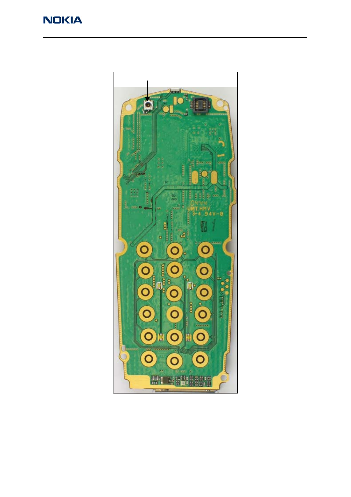
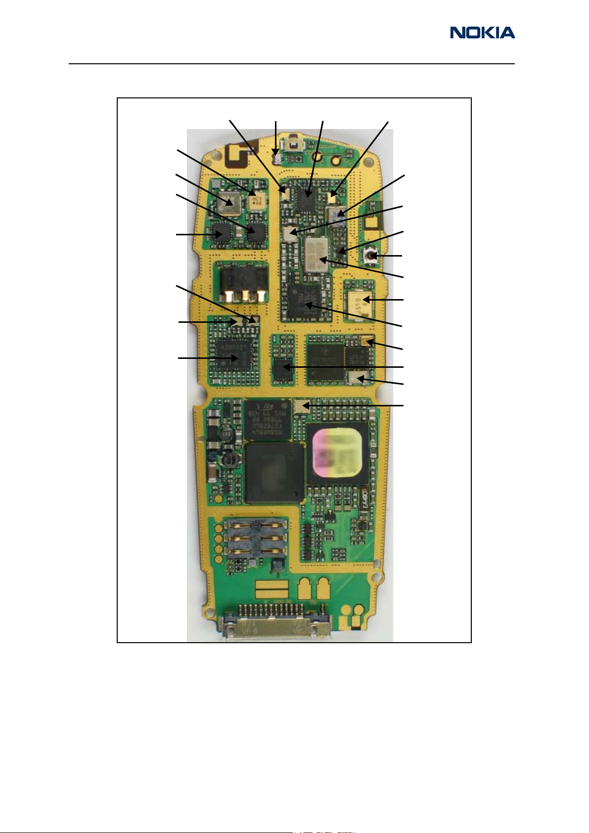
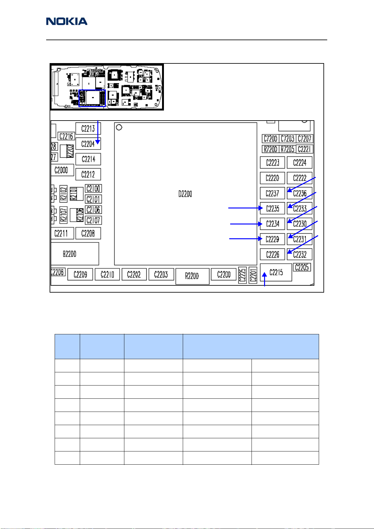
Component Layouts
Figure 1 and Figure 2 show the main components of the 2125/2125i/2126/2126i/2128i.
Cell RF connector
Figure 1: Component layout (top)
ISSUE 1 08/2005 ©2005 Nokia Corporation Company Confidential Page 3
2125/2125i/2126/2126i/2128i (RH-71)
RF Description and Troubleshooting
Cell Rx SAW filter
Cell duplexer
Diplexer
N7160 Rx
front-end IC
PCS Rx SAW
PCS duplexer
Cell PA
PCS PA
Cell Tx filter
PCS Tx filter
Tx upconverter
GPS RF filter (1)
AMPS IF
XTal filter
GPS LNA
GPS RF connector
CDMA IF
SAW filter
VCO
N7100 Rx
downconverter
GPS RF filter (2)
Synthesizer IC
GPS TCXO
VCTCXO
Figure 2: Component layout (bottom)
Page 4 ©2005 Nokia Corporation Company Confidential ISSUE 1 08/2005
2125/2125i/2126/2126i/2128i (RH-71)
Nokia Customer Care RF Description and Troubleshooting
Phoenix Setup
Use the following steps to configure Phoenix for RF troubleshooting.
1. Connect RF test connector to a call box.
2. Connect the mobile terminal to a PC via the bottom connector, and connect a
power supply.
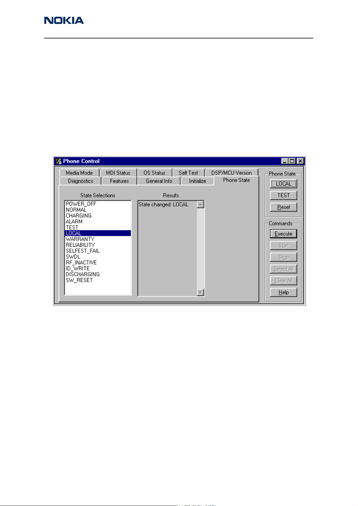
3. Open the Troubleshooting menu, and click Phone Control.
The Phone Control dialog box appears.
4. On the Phone Control dialog box, click the LOCAL button in the Phone State
area to put the mobile terminal into Local Mode.
Figure 3: Phone Control dialog box
5. Use Table 1, “Phoenix Configuration,” on page 6 to continue Phoenix
configuration based on the band type.
ISSUE 1 08/2005 ©2005 Nokia Corporation Company Confidential Page 5
2125/2125i/2126/2126i/2128i (RH-71)
RF Description and Troubleshooting Nokia Customer Care
Table 1: Phoenix Configuration
Cell PCS AMPS
1. On the RF Main Mode dialog box:
• Band = Cell (CDMA)
• Channel = 384
• Mode = Rx/Tx
2. Click Set. Be sure that the “RF Main Mode set successfully”
message appears in the status bar.
3. On the CDMA Control dialog box:
• State = Rho ON
• Band = Cell
• Radio Configuration = Mode 1: IS-95 Voice
• Select the Set default PDM values check box.
4. Click Execute.
5. Configure the spectrum analyzer using the following values:
• Center frequency = 836.52 MHz
• Span = 100 MHz
• Amplitude = 20 dBm
• Attenuation = Auto
• BW = Auto
6. Open the RF PDM Control dialog box, and click Read Phone.
Ensure the following values:
• Tx AGC1 = 0
• Tx AGC2 = -512
• PA Gain = 114
• Pout = +16 dBm
• Current = 360 mA
• Pout with AAS-10 at antenna connection = -8 dBm
1. On the RF Main Mode dialog box:
• Band = PCS (CDMA)
• Channel = 600
• Mode = Rx/Tx
2. Click Set. Be sure that the “RF Main Mode set successfully”
message appears in the status bar.
3. On the CDMA Control dialog box:
• State = Rho ON
• Band = PCS
• Radio Configuration = Mode 1: IS-95 Voice
• Select the Set default PDM values check box.
4. Click Execute.
5. Configure the spectrum analyzer using the following values:
• Center frequency = 1880 MHz
• Span = 100 MHz
• Amplitude = 20 dBm
• Attenuation = Auto
• BW = Auto
6. Open the RF PDM Control dialog box, and click Read Phone.
Ensure the following values:
• Tx AGC1 = 0
• Tx AGC2 = -512
• PA Gain = 207
• Pout = +8 dBm
• Current = 300 mA
• Pout with AAS-10 at antenna connection = -8 dBm
1. On the AMPS Control dialog box:
• Click the Tx Control tab.
• In the Set Channel field, type 384.
• In the Power Level field, type 2.
• Select the Transmitter ON option
2. Click Execute.
3. Configure the spectrum analyzer using the following values:
• Center Frequency = 836.52 MHz
• Span = 100 MHz
• Amplitude = 20 dBm
• Attenuation = Auto
• BW = Auto
4. Open the RF PDM Control dialog box, and click Read Phone.
Ensure the following values:
• Tx AGC1 = 0
• Tx AGC2 = -512
• PA Gain = -200
• Pout = +17 dBm
• Current = 370 mA
• Pout w/ AAS-10 at antenna connection = -8 dBm
Page 6 ©2005 Nokia Corporation Company Confidential ISSUE 1 08/2005
2125/2125i/2126/2126i/2128i (RH-71)
Nokia Customer Care RF Description and Troubleshooting
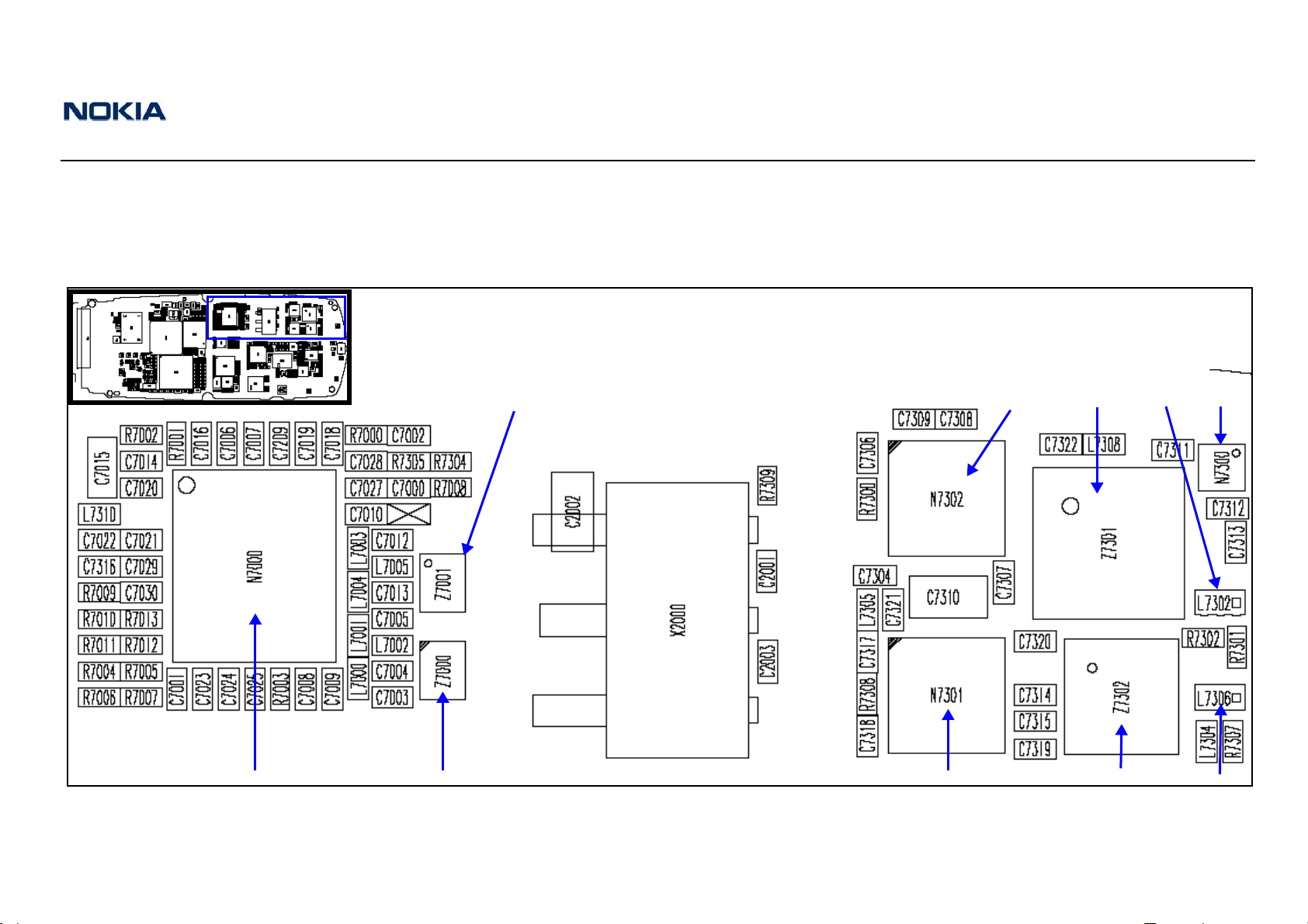
Tx Troubleshooting
Main Tx Components
N7000 TX IC
PCS TX SAW filter
Figure 4: Tx components
PCS
PCS PA
Cell PACell TX SAW filter
duplexer
Cell duplexer Cell coupler
PCS
coupler
Power
detector
ISSUE 1 08/2005 ©2005 Nokia Corporation Company Confidential Page 7
2125/2125i/2126/2126i/2128i (RH-71)
RF Description and Troubleshooting Nokia Customer Care
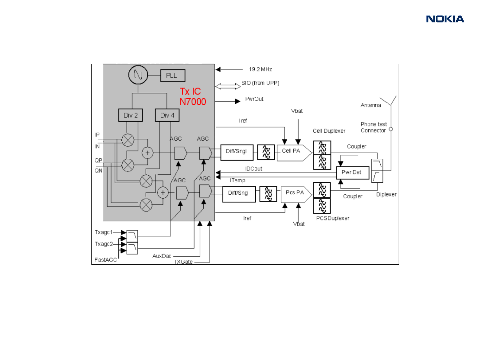
Cell Transmitter Block Diagram
Figure 5: Tx system block diagram
Page 8 ©2005 Nokia Corporation Company Confidential ISSUE 1 08/2005
2125/2125i/2126/2126i/2128i (RH-71)
Nokia Customer Care RF Description and Troubleshooting
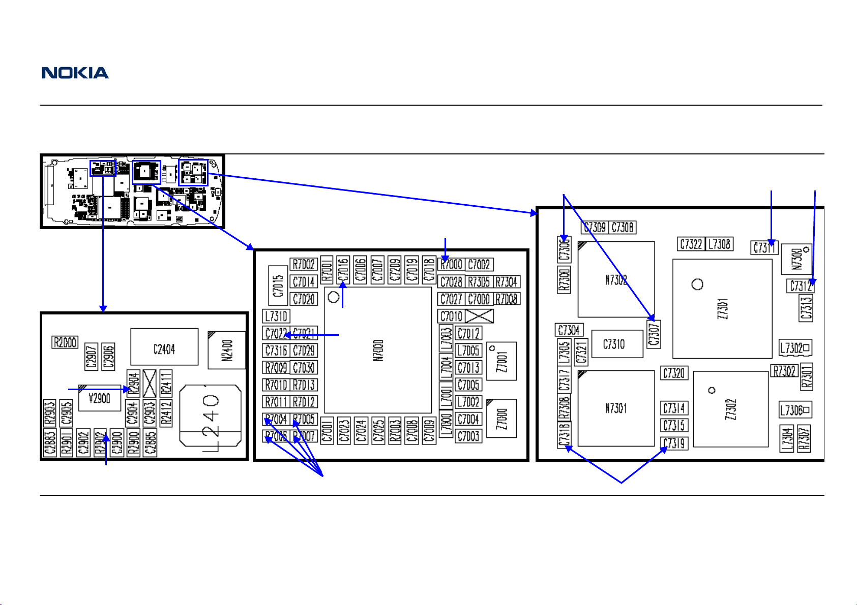
Tx DC Test Points
VBATT PCS
3
4
5
1
2
6
VBATT Cell
Figure 6: Tx DC test points
7 8
ISSUE 1 08/2005 ©2005 Nokia Corporation Company Confidential Page 9

2125/2125i/2126/2126i/2128i (RH-71)
RF Description and Troubleshooting
Table 2 shows the Tx DC test points shown in Figure 6.
Table 2: Tx DC Test Points
Test Point Description Value
1 AGC 1 From 0.1 to 1.8 V
2 AGC 2 From 0.1 to 1.8 V
3 VR6 2.8 V
4 Tx UHF LO lock voltage 1.2 V
5VR1B 4.8 V
6 Tx IQ in 1.2 V
7 VR2 (power detector) 2.76 V
8 Power detector output PCS:
With oscilloscope: 500 mV p-p
• 1.9 V at < 5 dBm
• 1.6 V at 15 dBm
• 0.8 V at 25 dBm
Cell:
• 1.9 V at < 5 dBm
• 1.7 V at 15 dBm
• 1.3 V at 25 dBm
Page 10 ©2005 Nokia Corporation Company Confidential ISSUE 1 08/2005
2125/2125i/2126/2126i/2128i (RH-71)
Nokia Customer Care RF Description and Troubleshooting
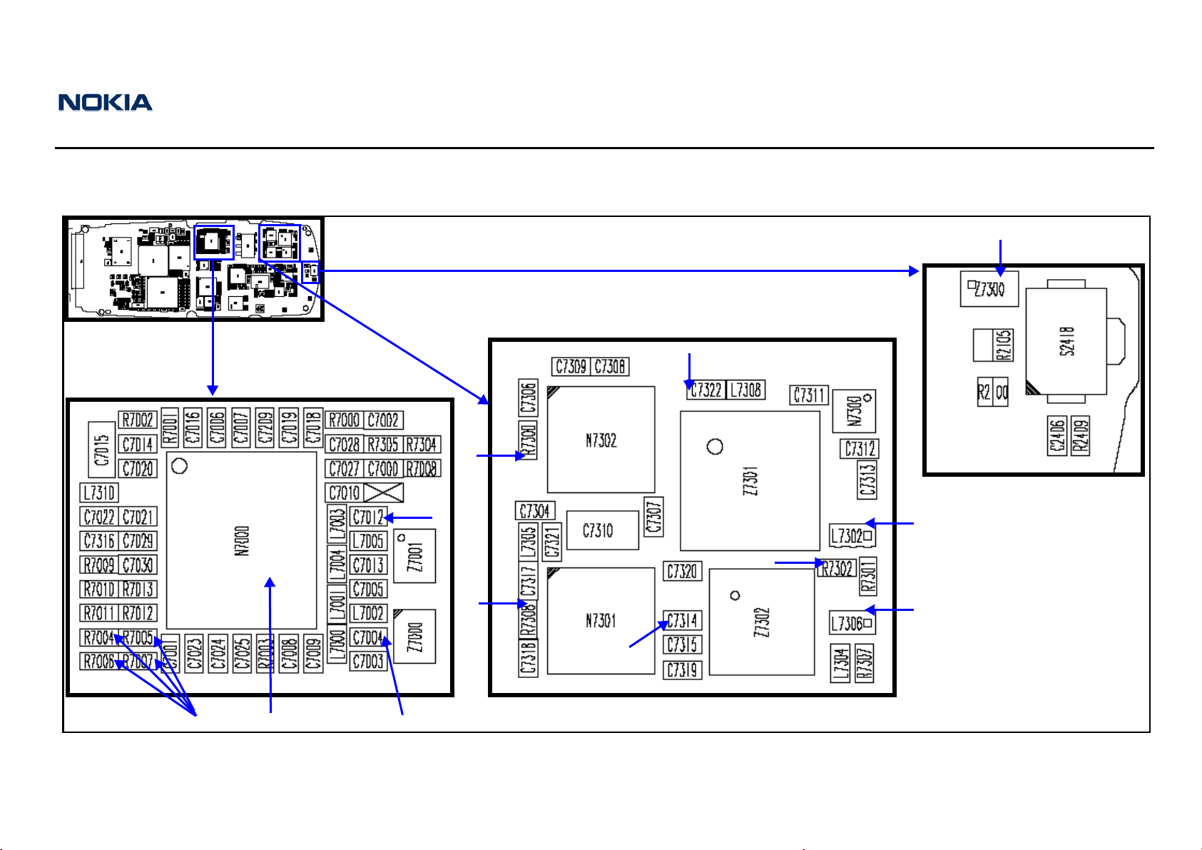
Tx RF Test Points
12
8
5
4
9
6
7
1
2
3
10
11
Figure 7: Tx RF Test Points
ISSUE 1 08/2005 ©2005 Nokia Corporation Company Confidential Page 11
2125/2125i/2126/2126i/2128i (RH-71)
RF Description and Troubleshooting
Table 3 shows the test points shown in Figure 7.
Table 3: Tx RF Test Points
Test Point Description Value
1 Tx IQ in with oscilloscope 500 mV p-p with +1.2 V offset
2 Tx UHF LO Cell: 3346.08 MHz, -57 dBm
3 Cell/AMPS N7000 out Cell: 836.25 MHz, -15 dBm
4 PCS N7000 out 1880 MHz, -22 dBm
5PCS PA in -23 dBm
6 Cell/AMPS PA in Cell: -15 dBm
7 Cell/AMPS PA out Cell: +11 dBm
PCS: 3760 MHz, -54 dBm
AMPS: 836.25 MHz, dBm
AMPS: -7 dBm
AMPS: +22 dBm
8 PCS PA out -2 dBm
9 Power detector in Cell: -8 dBm
AMPS: +3 dBm
PCS: -17 dBm
10 PCS coupler out -1 dBm
11 Cell/AMPS coupler out Cell: +8 dBm
AMPS: +18 dBm
12 Diplexer out Cell: +10 dBm
AMPS: +19 dBm
PCS: -17 dBm
Page 12 ©2005 Nokia Corporation Company Confidential ISSUE 1 08/2005
2125/2125i/2126/2126i/2128i (RH-71)
Nokia Customer Care RF Description and Troubleshooting
TX DC Test Points
1
2
3
Figure 8: Bottom side Tx DC test points
Table 4 shows the Tx DC test points shown in Figure 8.
Table 4: Tx DC Test Points and RF Supply Line Resistance to Ground
Test
Point
1 VIO 1.8 V
2 VR3 2.78 V (synthesizer)
Description Value RF Supply Lines Resistance to Ground*
Ω to ground
>1M
>500k
Ω to ground
4
6
8
10
N7100, N7000, UHF PLL
VCTCXO
5
7
9
3 VR7 2.78 V (Rx)
4 VR5 2.78 V (Rx)
5 VR4 2.78 V (Rx)
6 VR6 2.78 V (Tx)
7 VR2 2.78 V (Tx)
8 VR1B 4.75 V (Tx)
~500k
Ω to ground
3.2~5.1
4.3k
Ω to ground
300k
Ω to ground
7.5k
Ω to ground
Ω to ground
>100k
Ω to ground
N7100
N7160, N7100
VCO
N7000
N7000, PA detector
N7000
ISSUE 1 08/2005 ©2005 Nokia Corporation Company Confidential Page 13
2125/2125i/2126/2126i/2128i (RH-71)
RF Description and Troubleshooting
Table 4: Tx DC Test Points and RF Supply Line Resistance to Ground (Continued)
Test
Point
9 VR1A 4.75 V (synthesizer)
10 VBATT From 3.2 to 4.7 V
Description Value RF Supply Lines Resistance to Ground*
Ω to ground
>100k
V
RF1
REF
* Note: Always measure resistance with the phone powered off.
Ω to ground
45k
UHF PLL
N7100
Page 14 ©2005 Nokia Corporation Company Confidential ISSUE 1 08/2005
2125/2125i/2126/2126i/2128i (RH-71)
Nokia Customer Care RF Description and Troubleshooting
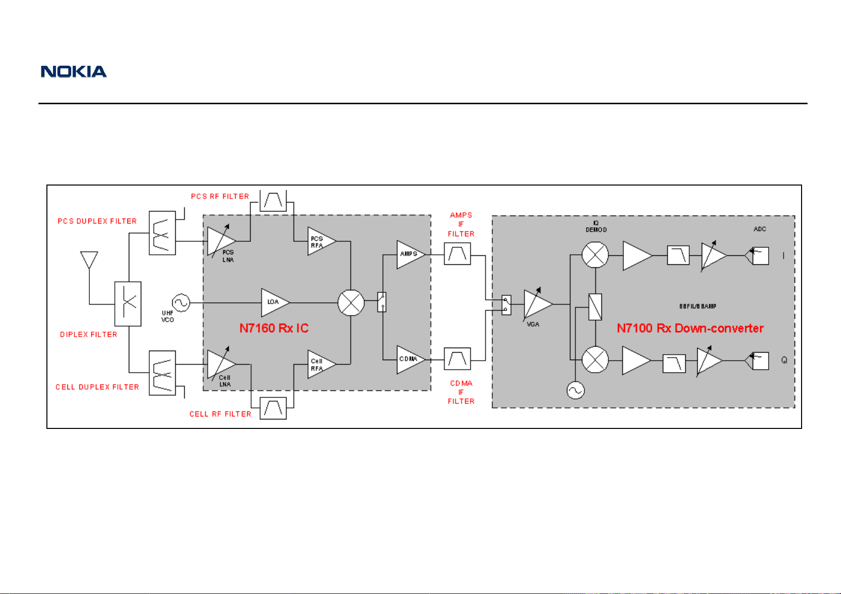
Receiver Troubleshooting
Rx System Block Diagram
Figure 9: Rx RF system diagram
ISSUE 1 08/2005 ©2005 Nokia Corporation Company Confidential Page 15
 Loading...