

Page 1

After Sales Technical Documentation
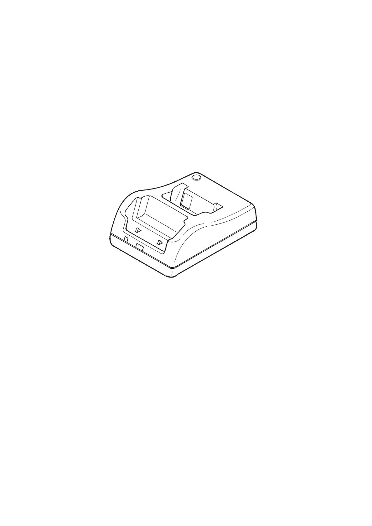
Desktop Charger
CHH–2
Original 50/96
NMP Part No. 0275272
Page 2

After Sales
Desktop Charger CHH–2
CONTENTS
Desktop Charger CHH–2 – 3. . . . . . . . . . . . . . . . . . . . . . . . . . . . . . . .
General – 3. . . . . . . . . . . . . . . . . . . . . . . . . . . . . . . . . . . . . . . . . . . . .
Technical Summary – 3. . . . . . . . . . . . . . . . . . . . . . . . . . . . . . . . . . .
Operation – 3. . . . . . . . . . . . . . . . . . . . . . . . . . . . . . . . . . . . . . . . .
Charging Indication – 4. . . . . . . . . . . . . . . . . . . . . . . . . . . . . . . . .
Technical Specifications – 4. . . . . . . . . . . . . . . . . . . . . . . . . . . . . . .
Charge States and Charge Control – 4. . . . . . . . . . . . . . . . . . .
External Signals and Connections – 5. . . . . . . . . . . . . . . . . . . .
Fast Travel Charger Connector X130 – 5. . . . . . . . . . . . . . .
Phone Charging Connectors X110, X111 – 5. . . . . . . . . . . .
Spare Battery Connector X120 – 5. . . . . . . . . . . . . . . . . . . .
Circuit Description – 6. . . . . . . . . . . . . . . . . . . . . . . . . . . . . . . . . . . .
Control Logic – 6. . . . . . . . . . . . . . . . . . . . . . . . . . . . . . . . . . . . . .
Prosessor Input/Output Signals – 6. . . . . . . . . . . . . . . . . . . . . .
Processor A/D Inputs – 6. . . . . . . . . . . . . . . . . . . . . . . . . . . . . . .
Charging the Spare Battery – 7. . . . . . . . . . . . . . . . . . . . . . . . . .
Discharging the Spare Battery – 7. . . . . . . . . . . . . . . . . . . . . . .
Watchdog Circuit – 7. . . . . . . . . . . . . . . . . . . . . . . . . . . . . . . . . . .
Block Diagram – 9. . . . . . . . . . . . . . . . . . . . . . . . . . . . . . . . . . . . . . .
Circuit Diagram – 10. . . . . . . . . . . . . . . . . . . . . . . . . . . . . . . . . . . . . .
Layout and Foil Diagrams – 11. . . . . . . . . . . . . . . . . . . . . . . . . . . . .
Parts List (Version 1.6) Code: 0200184 – 12. . . . . . . . . . . . . . . .
Exploded View – 15. . . . . . . . . . . . . . . . . . . . . . . . . . . . . . . . . . . . . . .
Assembly Parts – 15. . . . . . . . . . . . . . . . . . . . . . . . . . . . . . . . . . . . . .
Technical Documentation
Page – 2
Original 50/96
Page 3
After Sales
Technical Documentation
Desktop Charger CHH–2
General
The CHH–2 desktop charger is designed for the charging of the handportable phone and a spare battery. In a standard configuration rapid charging is possible by connecting the desktop charger to an ac power outlet
via a suitable constant current ac adapter (ACH–4). This must be connected to the d.c. connector, X130.
Desktop Charger CHH–2
Technical Summary
Operation
The device has a d.c. plug input connector for ACH–4 charger and 2– and
4–pin output connectors for the phone and extra battery. Charging takes
place at a battery temperatures of 5...45 Centigrade. Charge control of
the phone is done with phone microprocessor and charge control of extra
battery is done with separate microprocessor located in a desktop stand.
Phone is always charged first, then extra battery.
A battery gives better capacity if it is occasionally discharged completely.
User can do this by using the ‘deep discharge‘ –feature of CHH–2. This
feature is provided only extra battery slot and pressing the ‘discharge‘
–button. The extrabattery will then automatically be discharged and
charged to full. If this button is pressed twice then the discharge function
is cancelled.
Original 50/96
Page – 3
Page 4

After Sales
Desktop Charger CHH–2
Charging Indication
Charge is indicated with two dual–colors led‘s, one for the phone and one
for the extra battery pack. The liquid–crystal display of the phone also
contains a three–bar battery display.
Led‘s are dim when there is no phone or extra battery connected.
Right led for handportable:
Red phone led indicates a fast charge mode of the phone battery.
Green phone led indicates a tricle (maintenance) charge mode of the
phone battery; with steady lcd battery display it means that the battery is
full. If the led is green but the battery display is scrolling, charging is disabled due to battery temperature (less than +5 or more than +45 Centigrade).
Left led for spare battery:
Red spare battery led indicates that the battery is not full; either there is a
fast charge mode active or charging is disabled due to a battery temperature or to fast charge mode of the phone.
Technical Documentation
Green spare battery led indicates that the battery is full.
Flashing red spare battery led indicates that a discharge cycle is acti-
vated.
Technical Specifications
Charge States and Charge Control
Charge current for the phone is supplied through a series switch transistor in the phone. When this transistor is on the charger is supplying a
constant current to the phone. This is the rapid charge mode.
When the transistor is off no current is supplied to the phone and the
charger is in the constant voltage mode.
Having been charged up in the rapid charge mode, the battery is kept in
full charge using pulsed charging, i.e. switching power alternately on and
off at a variable duty cycle and a frequency of a few Hz.
The desktop charger is also provided with control logic for spare battery
charging, which is allowed when no phone is connected or when the
phone is in the pulsed charge mode.
Page – 4
Original 50/96
Page 5

After Sales
Technical Documentation
External Signals and Connections
The charger has three external connectors, the AC fast travel charger
connector, the phone charging connector and the spare battery connector.
Fast Travel Charger Connector X130
Pin: Name: Description:
1 VDC Supply voltage input
2 GND Common ground
Phone Charging Connectors X110, X111
Pin: Name: Description:
X110 VC Charge voltage output
Desktop Charger CHH–2
X111 PDET/GND Charge detect/phone common ground
Spare Battery Connector X120
Pin/X120: Pin/out: Name: Description:
6, 7, 8 1 VBAT Positive terminal of battery
5 2 BSI Battery size indicator
4 3 BTEMP Battery temperature sensing
input
1, 2, 3 4 GND Common ground
Original 50/96
Page – 5
Page 6

After Sales
Desktop Charger CHH–2
Circuit Description
The DC2 desktop charger module consists of microcomputer based control logic for spare battery charging and discharging. It also has power
outlet for transportable phone.
Control Logic
Charging is controlled by processor D150. It is a single–chip type controller incorporating RAM, ROM, A/D converter, and a multifunction timer/
counter.
Prosessor Input/Output Signals
Name: Function:
PA0 Phone LED control, green: ”1”
Technical Documentation
PA1 Phone LED control, red: ”1”
PA2 Spare battery LED control, green: ”1”
PA3 Spare battery LED control, red: ”1”
PA4/DBIN Discharge button input, ”0”: start discharge
PA5/DISW Discharge control output, ”1”: discharge enabled
PA6/BSW Spare battery charge control, ”0”: charge disabled,
PC7 Watchdog reset output
Processor A/D Inputs
Name: Function:
AN0/VBATL Battery voltage
AN1/VBATH High resolution battery voltage
”1”: rapid charge, PWM: pulsed mode
• range: 0...11 V
• resolution: 43 mV/bit
• range 7...11 V
• resolution: 16 mV/bit
Page – 6
AN2/PDET Phone current detect
• PDET = ”1” for A/D value higher than 5
• PDET = ”0” for A/D value 5 of or less
AN3/BTEMP Battery temperature, 27 kΩ pull–up resistor to
+5 V reference voltage
AN4/BSI Battery size, 100 kΩ pull–up resistor to +5 V
reference voltage
Original 50/96
Page 7

After Sales
Technical Documentation
AN5/CHVOL Charger voltage detection
AN7/LIREF Lithium reference voltage input
• range: 0...5 V
• resolution: 19.5 mV/bit
Charging the Spare Battery
Charging current for the spare battery is fed in via switching transistor
V130 and Schottky diode V131. The transistor is controlled by the processor (BSW line). When the transistor is on, a constant current is supplied
to the battery. This is the rapid charging mode. In the pulsed charging
mode, charging current is adjusted by pulsing this rapid charge current.
Battery voltage is measured through resistor divider R143/R144 (100/121
kohm). The range measured is 0 to 11 V; a voltage variation of 43 mV can
be detected. For improved resolution, i.e. rapid charge cut off, operational
amplifier N140 is added. This amplifies the battery voltage by a factor of
(1 + 100 kohm/56 kΩ) and compares the result to a +5 V reference supply. The A/D converter receives a battery voltage range of 7.0 to 11 V; a
better resolution of 16 mV results.
Desktop Charger CHH–2
Battery size is determined by reading the BSI line state. This is pulled to
+5 V reference voltage by R147 (100 kΩ). In the battery pack a ”size” resistor is connected between BSI and GND.
Temperature is measured over the BTEMP line. This line is pulled to +5 V
reference voltage by R145 (27 kΩ). In the battery pack an NTC resistor is
connected between BTEMP and GND.
Because the phone and the spare battery cannot be charged at the same
time the charging current of the phone must be detected. This is done at
the A/D input AN2 (PDET). The charging current for the phone is directed
through series diode V114. If the voltage drop across the diode is higher
than 100 mV (corresponds to A/D value of 5), charging current is flowing
to the phone.
The CHH–2 desktop charger has two dual–colour LEDs to indicate the
charging states of the phone and the spare battery.
Discharging the Spare Battery
The desktop charger is also provided with a discharge function. This is
activated by pressing a discharge switch on top of the charger. The spare
battery is then discharged before charging. Resistors R181–R188 determines the discharge current which is fed through switching transistor
V134 controlled by processor over the DISW line (pin 64). The battery is
discharged to 5 V and thereafter charged normally. The state of the discharge switch is read via the DBIN line (pin 63).
Watchdog Circuit
The processor generates positive pulses to output PC7 (pin 18). These
pulses are received by transistor V201 discharging capacitor C161. The
Original 50/96
Page – 7
Page 8

After Sales
Desktop Charger CHH–2
capacitor is charged through resistor R163. This voltage is fed to regulator N100 shutdown input (pin 3) through transistor V162.The 5V reference
supply is generated by regulator N100.If the processor stops the voltage
across the capacitor increases and the regulator is switched off.
Technical Documentation
Page – 8
Original 50/96
Page 9

After Sales
Technical Documentation
Block Diagram
RAPID CHARGER
CONNECTOR (X130)
1
3
2
800mA OUT
Desktop Charger CHH–2
PHONE CHARGING
CONNECTOR (X110)
VC
PDET/GND
R
GND
SPARE BATTERY
CONNECTOR (X120)
VBAT
BSI
BTEMP
GND
GND
GND
DISCHARGE
START
BUTTON
GND GND
PHONE CHARGE
INDICATION
RED/GREEN LED
MICROPROCESSOR/CONTROL LOGIC
A/D–INPUTS
PHONE DETECT
CHARGER VOLTAGE
BATTERY VOLTAGE
BATTERY SIZE
BATTERY TEMP.
DISCHARGE START
R
D–OUTPUTS
CHARGE CONTROL
PHONE LED1
PHONE LED2
SPARE BAT.LED1
SPARE BAT.LED2
DISCHARGE CONTROL
SPARE BATTERY CHARGE
INDICATION
RED/GREEN LED
Original 50/96
Page – 9
Page 10

After Sales
Desktop Charger CHH–2
Circuit Diagram
Technical Documentation
Page – 10
Original 50/96
Page 11

After Sales
Technical Documentation
Layout and Foil Diagrams
Desktop Charger CHH–2
Original 50/96
Page – 11
Page 12

After Sales
Desktop Charger CHH–2
Technical Documentation
Parts List (Version 1.6) Code: 0200184
ITEM CODE DESCRIPTION VALUE TYPE
R100 1413603 Chip resistor 47 k 5 % 0.1 W 0805
R106 1412286 Chip jumper 0805
R107 1411669 Chip resistor 22 5 % 0.1 W 0805
R108 1411669 Chip resistor 22 5 % 0.1 W 0805
R109 1415872 Melf resistor 120 1 % 0.2 W 0204
R110 1415872 Melf resistor 120 1 % 0.2 W 0204
R111 1412609 Chip resistor 27 k 5 % 0.1 W 0805
R117 1413829 Chip resistor 10 5 % 0.1 W 0805
R130 1413603 Chip resistor 47 k 5 % 0.1 W 0805
R131 1412310 Chip resistor 470 5 % 0.1 W 0805
R132 1414029 Chip resistor 3.3 k 5 % 0.1 W 0805
R133 1412310 Chip resistor 470 5 % 0.1 W 0805
R134 1412310 Chip resistor 470 5 % 0.1 W 0805
R135 1412430 Chip resistor 10 k 5 % 0.1 W 0805
R136 1413603 Chip resistor 47 k 5 % 0.1 W 0805
R138 1413603 Chip resistor 47 k 5 % 0.1 W 0805
R140 1416160 Melf resistor 100 k 1 % 0.2 W 0204
R141 1416040 Melf resistor 56.2 k 1 % 0.2 W 0204
R142 1413603 Chip resistor 47 k 5 % 0.1 W 0805
R143 1416160 Melf resistor 100 k 1 % 0.2 W 0204
R144 1416202 Melf resistor 121 k 1 % 0.2 W 0204
R145 1412609 Chip resistor 27 k 5 % 0.1 W 0805
R146 1413603 Chip resistor 47 k 5 % 0.1 W 0805
R147 1413635 Chip resistor 100 k 5 % 0.1 W 0805
R148 1413603 Chip resistor 47 k 5 % 0.1 W 0805
R149 1414029 Chip resistor 3.3 k 5 % 0.1 W 0805
R150 1414029 Chip resistor 3.3 k 5 % 0.1 W 0805
R151 1413635 Chip resistor 100 k 5 % 0.1 W 0805
R152 1413924 Chip resistor 220 5 % 0.1 W 0805
R153 1413924 Chip resistor 220 5 % 0.1 W 0805
R154 1414029 Chip resistor 3.3 k 5 % 0.1 W 0805
R155 1414029 Chip resistor 3.3 k 5 % 0.1 W 0805
R156 1414029 Chip resistor 3.3 k 5 % 0.1 W 0805
R157 1414029 Chip resistor 3.3 k 5 % 0.1 W 0805
R158 1412729 Chip resistor 33 k 5 % 0.1 W 0805
R160 1413603 Chip resistor 47 k 5 % 0.1 W 0805
R161 1412430 Chip resistor 10 k 5 % 0.1 W 0805
R162 1413924 Chip resistor 220 5 % 0.1 W 0805
R163 1414244 Chip resistor 2.2 M 5 % 0.1 W 0805
R164 1414244 Chip resistor 2.2 M 5 % 0.1 W 0805
R170 1414533 Chip resistor 56 k 1 % 0.1 W 0805
R171 1414477 Chip resistor 12 k 1 % 0.1 W 0805
R172 1413603 Chip resistor 47 k 5 % 0.1 W 0805
Page – 12
Original 50/96
Page 13

After Sales
Technical Documentation
R181 1415576 Melf resistor 301 1 % 0.2 W 0204
R182 1415576 Melf resistor 301 1 % 0.2 W 0204
R183 1415576 Melf resistor 301 1 % 0.2 W 0204
R184 1415576 Melf resistor 301 1 % 0.2 W 0204
R185 1415576 Melf resistor 301 1 % 0.2 W 0204
R186 1415576 Melf resistor 301 1 % 0.2 W 0204
R187 1415576 Melf resistor 301 1 % 0.2 W 0204
R188 1415576 Melf resistor 301 1 % 0.2 W 0204
R191 1416107 Melf resistor 5.62 k 1 % 0.2 W 0204
R192 1416040 Melf resistor 56.2 k 1 % 0.2 W 0204
R193 1411490 Chip resistor 100 5 % 0.12 W 1206
R198 1411490 Chip resistor 100 5 % 0.12 W 1206
C102 2604209 Tantalum cap. 1.0 u 20 % 16 V 3.2x1.6x1.6
C103 2307816 Ceramic cap. 47 n 20 % 25 V 0805
C104 2309475 Ceramic cap. 47 n 10 % 50 V 1206
C105 2604110 Tantalum cap. 10 u 20 % 25 V 7.3x4.4x2.8
C129 2310336 Ceramic cap. 18 p 5 % 50 V 0805
C130 2310336 Ceramic cap. 18 p 5 % 50 V 0805
C131 2310336 Ceramic cap. 18 p 5 % 50 V 0805
C132 2310336 Ceramic cap. 18 p 5 % 50 V 0805
C133 2310336 Ceramic cap. 18 p 5 % 50 V 0805
C134 2307816 Ceramic cap. 47 n 20 % 25 V 0805
C135 2310336 Ceramic cap. 18 p 5 % 50 V 0805
C136 2310336 Ceramic cap. 18 p 5 % 50 V 0805
C137 2310336 Ceramic cap. 18 p 5 % 50 V 0805
C140 2307816 Ceramic cap. 47 n 20 % 25 V 0805
C141 2307816 Ceramic cap. 47 n 20 % 25 V 0805
C142 2307816 Ceramic cap. 47 n 20 % 25 V 0805
C143 2307816 Ceramic cap. 47 n 20 % 25 V 0805
C150 2307816 Ceramic cap. 47 n 20 % 25 V 0805
C151 2310343 Ceramic cap. 22 p 5 % 50 V 0805
C152 2310343 Ceramic cap. 22 p 5 % 50 V 0805
C153 2604209 Tantalum cap. 1.0 u 20 % 16 V 3.2x1.6x1.6
C154 2307816 Ceramic cap. 47 n 20 % 25 V 0805
C155 2310738 Ceramic cap. 4.7 n 20 % 50 V 0805
C160 2307816 Ceramic cap. 47 n 20 % 25 V 0805
C161 2604209 Tantalum cap. 1.0 u 20 % 16 V 3.2x1.6x1.6
C170 2307816 Ceramic cap. 47 n 20 % 25 V 0805
B150 4500822 Crystal 11.0592 M CL30PF H=3.6MM
V114 4110074 Schottky diode STPS340U 40 V 3 A SOD6
V129 4100077 Schottky diode BAS85 30 V 200 mA SOD80
V130 4210092 Transistor BCP69 pnp 20 V 1 A SOT223
V131 4110074 Schottky diode STPS340U 40 V 3 A SOD6
V132 4200917 Transistor BC848B/BCW32 npn 30 V 100 mA SOT23
V134 4200226 Darl. transistor BCV27 npn 30 V 300 mA SOT23
V140 4100567 Sch. diode x 2 BAS70–04 70V15 mA SERSOT23
V141 4106992 Zener diode BZX84 5 % 8.2 V 0.3 W SOT23
Desktop Charger CHH–2
Original 50/96
Page – 13
Page 14

After Sales
Desktop Charger CHH–2
V152 4200917 Transistor BC848B/BCW32 npn 30 V 100 mA SOT23
V153 4200917 Transistor BC848B/BCW32 npn 30 V 100 mA SOT23
V154 4200917 Transistor BC848B/BCW32 npn 30 V 100 mA SOT23
V155 4200917 Transistor BC848B/BCW32 npn 30 V 100 mA SOT23
V162 4200917 Transistor BC848B/BCW32 npn 30 V 100 mA SOT23
V170 4100567 Sch. diode x 2 BAS70–04 70V15 mA SERSOT23
V181 4864378 Led Green V 0805
V182 4864380 Led Red 2.2 V 0805
V183 4864378 Led Green V 0805
V184 4864380 Led Red 2.2 V 0805
V201 4200917 Transistor BC848B/BCW32 npn 30 V 100 mA SOT23
D150 4370104 IC, ROM MCU16/8 QFP64
N100 4301062 IC, regulator LP2951AC SO8S
N140 4309576 IC, 2 x op.amp. TLC27M2I SO8
S130 5200914 Push button switch 2–pole 6x7 smd SMD
X120 5431702 Flexfoil connect 1x08 1mm smd
5402366 Power jack 12v 0.5a for 3.8mmplug 3.8MMPLUG
9853917 PCB DC2 91.5X56.3X1.6 D 4/PA
9853917 PC board DC2 91.5x56.3x1.6 d 4/pa
Technical Documentation
Page – 14
Original 50/96
Page 15

After Sales
Technical Documentation
Exploded View
Desktop Charger CHH–2
Assembly Parts
ITEM Q’TY CODE DESCRIPTION VALUE, TYPE
1 9460089 Discharge button 4D 22992
2 9450259 Front cover 1D 22990
3 5461000 Battery connector 1x04
4 9460088 Light guide 3D 22993
5 9450260 Bottom cover 1D 22991
6 4 6501067 Adhesive foot d=8.0 h=2.0
7 3 6293012 PT screw KB22x8 FeZn
8 9380154 Label blank 4D 22419
C1 0200184 Charging module DC2
Original 50/96
Page – 15
Page 16

After Sales
Desktop Charger CHH–2
Technical Documentation
[This page intentionally left blank]
Page – 16
Original 50/96
 Loading...