

DATA SHEET
MOS INTEGRATED CIRCUIT
µ
PD17062
4-BIT SINGLE-CHIP MICROCONTROLLER CONTAINING PLL FREQUENCY
SYNTHESIZER AND IMAGE DISPLAY CONTROLLER
The µPD17062 is a 4-bit CMOS microcontroller for digital tuning systems. The single-chip device
incorporates an image display controller enabling a range of different displays, together with a PLL frequency
synthesizer.
The CPU has six main functions: 4-bit parallel addition, logic operation, multiple bit test, carry-flag set/
reset, powerful interrupt, and a timer.
The device contains a user-programmable image display controller (IDC) for on-screen displays. The
different displays can be controlled with simple programs.
The device also has a serial interface function, many input/output (I/O) ports controlled by powerful I/O
instructions, and 6-bit pulse width modulation (PWM) output for a 4-bit A/D converter and D/A converter.
FEATURES
• 4-bit microcontroller for digital tuning system
• Internal PLL frequency synthesizer: With prescaler
µ
PB595
•5 V ±10%
• Low-power CMOS
• Program memory (ROM): 8K bytes (16 bits × 3968
steps)
• Data memory (RAM): 4 bits × 336 words
• 6 stack levels
• 35 easy-to-understand instruction sets
• Support of decimal operations
µ
• Instruction execution time: 2
crystal)
• Internal D/A converter: 6 bits × 4 (PWM output)
• Internal A/D converter: 4 bits × 6
• Internal horizontal synchronizing signal counter
• Internal commercial power frequency counter
• Internal power-failure detector and power-on reset
circuit
s (with an 8-MHz
• Internal image display controller (IDC) (user-pro-
grammable)
Number of characters in display: Up to 99 on a
single screen
Display configuration: 14 rows × 19 columns
Number of character types: 120
Character format: 10 × 15 dots (rimming possible)
Number of colors: 8
Character size: Four sizes in each of the horizontal
and vertical dimensions
Internal 1H circuit for preventing vertical deflection
• Internal 8-bit serial interface (One system with two
channels: three-wire or two-wire)
• Interrupt input for remote-controller signals (with
noise canceler)
• Many I/O ports
Number of I/O ports : 15
Number of input ports : 4
Number of output ports: 8
Document No. IC-3560
(O.D. No. IC-8937)
Date Published January 1995 P
Printed in Japan
The information in this document is subject to change without notice.
©
1995
µ
ORDERING INFORMATION
Part number Package
µ
PD17062CU-××× 48-pin plastic shrink DIP (600 mil)
µ
PD17062GC-××× 64-pin plastic QFP (14 × 14 mm)
Remark ××× is the ROM code number.
FUNCTION OVERVIEW
Item Function
ROM (program memory) capacity 3968 × 16 bits (masked ROM)
CROM (character ROM) capacity 1920 × 16 bits (included in ROM)
RAM (data memory) capacity 336 × 4 bits (including the area that can be used for VRAM)
VRAM (video RAM) capacity 224 × 4 bits (included in RAM)
Instruction execution time 2 µs (when the 8-MHz crystal is used)
Stack level 6 levels (stack operation possible)
Number of I/O ports Number of input ports: 4
Number of output ports: 8
Number of I/O ports: 15
IDC (Image Display Controller) Number of characters in display: Up to 99 on a single screen
Display format: 10 × 15 dots, 14 rows × 19 columns
Number of character types: 120 (user-programmable)
Number of colors: 8
Character size
Vertical dimension : 1 to 4 times (can be set for each line)
Horizontal dimension : 1 to 4 times (can be set for each character)
Serial interface Serial interface 0 (two-wire or I2C bus compatible)
D/A converter 6 bits × 4 (PWM output, withstand voltage of up to 12.5 V)
A/D converter 4 bits × 6 (successive-approximation converter by software)
Interrupt External interrupt : 2 channels
Timer 1 channel (internal clock/zerocross input)
PLL frequency synthesizer Scaling method : Pulse swallow method (VCO pin: Up to 40 MHz),
Reset Power-on reset
Supply voltage 5 V ±10%
One system
4 channels
Reference frequency : 6.25, 12.5, 25 kHz
Charge pump : Error-out output
Phase comparator : Capable of unlock detection by a program
Reset by the CE pin
With power-failure detection function
Serial interface 1 (two-wire or three-wire)
Internal interrupt : 2 channels
external specialized two-modulus prescaler
(µPB595, for example)
PD17062
2
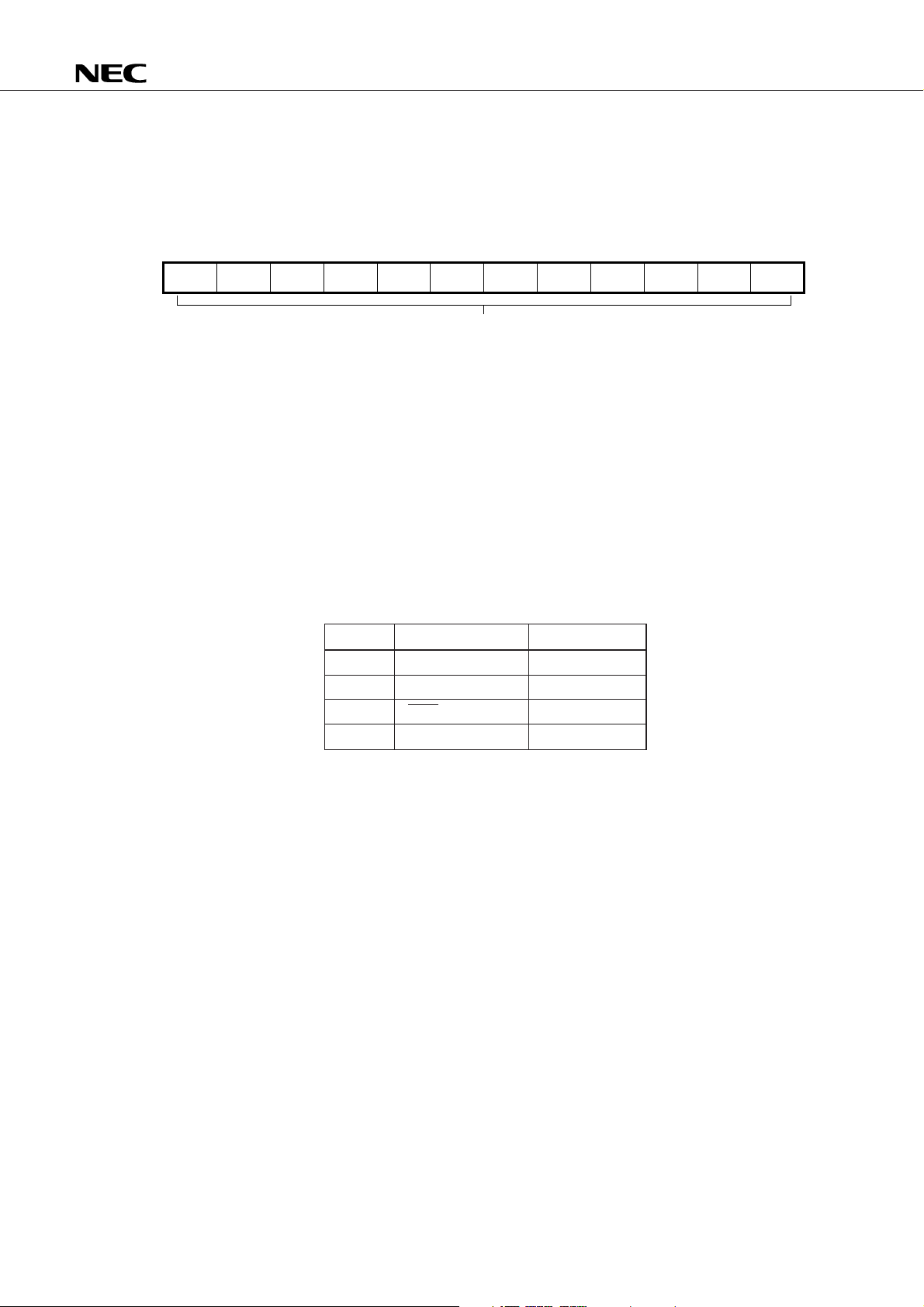
PIN CONFIGURATION (TOP VIEW)
48-pin plastic shrink DIP (600 mil)
µ
PD17062
P0C3
P0C2
P0C1
P0C0
P0D3/ADC5
P0D2/ADC4
P0D1/ADC3
P0D0/ADC2
PWM3
PWM2
PWM1
PWM0
VDD
VCO
EO
GND
PSC
CE
OUT
X
XIN
P1A3
P1A2
P1A1
P1A0
1
2
3
4
5
6
7
8
9
10
11
12
13
14
15
16
17
18
19
20
21
22
23
24
µ
PD17062CU-×××
48
47
46
45
44
43
42
41
40
39
38
37
36
35
34
33
32
31
30
29
28
27
26
25
INTNC
0/SDA
P0A
P0A1/SCL
P0A2/SCK
3/SO
P0A
0/SI
P0B
P0B
1
2/TMIN
P0B
P0B3/HSCNT
0
ADC
P1C1
P1C2
P1C3/ADC1
VSYNC
HSYNC
BLANK
BLUE
GREEN
RED
P1B0
1
P1B
P1B2
3
P1B
GND
0 to ADC5 : A/D converter input P0D0 to P0D3 : Port 0D
ADC
BLANK : Blanking signal output P1A
BLUE : Character signal output P1B
CE : Chip enable P1C
0 to P1A3 : Port 1A
0 to P1B3 : Port 1B
1 to P1C3 : Port 1C
EO : Error out RED : Character signal output
GND : Ground SCK : Shift clock input/output
GREEN : Character signal output SCL : Shift clock input/output
HSCNT : Horizontal synchronizing signal SDA : Serial data input/output
counter input SI : Serial data input
H
SYNC : Horizontal synchronizing signal input SO : Serial data output
NC : Interrupt signal input TMIN : Timer event input
INT
NC : No connection VCO : Local oscillation input
PSC : Pulse swallow control output V
PWM
0 to PWM3 : Pulse width modulation output VSYNC : Vertical synchronizing signal input
0 to P0A3 : Port 0A XIN : Clock oscillation
P0A
P0B
0 to P0B3 : Port 0B XOUT : Clock oscillation
P0C
0 to P0C3 : Port 0C
DD : Main power supply
3
64-pin plastic QFP (14 × 14 mm)
µ
PD17062
P0D
0
/ADC
PWM
PWM
PWM
NC
PWM
NC
NC
V
NC
3
/ADC
1
P0D
4
/ADC
2
P0D
5
/ADC
3
P0D
0
P0C
1
P0C
2
P0C
3
P0C
NC
NC
NC
INT
/SDA
0
P0A
/SCL
1
P0A
/SCK
1
P0A
/SO
3
P0A
/SI
0
P0B
1
P0B
64 63 62 61 60 59 58 57 56 55 54 53 52 51 50 49
2
3
2
1
1
2
3
4
5
0
6
7
8
PD17062GC-×××-3BE
µ
DD
9
10
48
47
46
45
44
43
42
41
40
39
POB
2
/TMIN
POB3/HSCNT
ADC
0
P1C
1
NC
P1C
2
NC
NC
NC
NC
VCO
NC
EO
NC
GND
PSC
11
12
13
14
15
16
17 18 19 20 21 22 23 24 25 26 27 28 29 30 31 32
0
CE
OUT
X
IN
X
2
P1A3P1A
NC
1
P1A
P1A
NC
GND
3
P1B
2
P1B
1
P1B
0
P1B
RED
38
37
36
35
34
33
GREEN
P1C
3
/ADC
NC
V
SYNC
H
SYNC
BLANK
BLUE
1
4
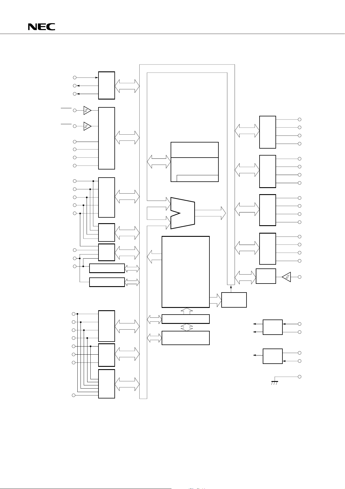
BLOCK DIAGRAM
VCO
PSC
EO
SYNC
H
V
SYNC
RED
GREEN
BLUE
BLANK
0
/SDA
P0A
1
/SCL
P0A
2
/SCK
P0A
3
/SO
P0A
P0B
0
/SI
PLL
IDC
Serial
I/O
RF
RAM
336 × 4 bits
(Including VRAM)
SYSREG
ALU
PWM
P1A
P1B
µ
PD17062
PWM
PWM
PWM
PWM
P1A
P1A
P1A
P1A
P1B
P1B
P1B
P1B
0
1
2
3
0
1
2
3
0
1
2
3
P0B2/TMIN
3
/HSCNT
P0B
P0D
0
/ADC
P0D1/ADC
P0D2/ADC
P0D3/ADC
P1C3/ADC
P0B
P1C
P1C
ADC
P0A
1
P0B
Hsync Counter
ROM
3968 × 16 bits
(Including CROM)
Timer Controller
P0C
Interrupt
Controller
P0C
P0C
P0C
P0C
INT
0
1
2
3
NC
Instruction
Decoder
2
3
4
5
1
2
1
P0D
P1C
Program Counter
Stack 6 × 12 bits
CPU
Peripheral
OSC
Reset
X
X
V
CE
IN
OUT
DD
GND
A/D
0
5

µ
PD17062
CONTENTS
1. PINS ............................................................................................................................................. 11
1.1 PIN FUNCTIONS ............................................................................................................................. 11
1.2 EQUIVALENT CIRCUITS OF THE PINS ........................................................................................ 14
2. PROGRAM MEMORY (ROM) .................................................................................................... 18
2.1 CONFIGURATION OF PROGRAM MEMORY............................................................................... 18
2.2 FUNCTIONS OF PROGRAM MEMORY ........................................................................................ 19
2.3 PROGRAM FLOW ........................................................................................................................... 19
2.4 BRANCHING A PROGRAM ............................................................................................................ 20
2.6 TABLE REFERENCE ........................................................................................................................ 24
2.7 NOTES ON USING THE BRANCH INSTRUCTION AND
SUBROUTINE CALL INSTRUCTION ............................................................................................. 24
3. PROGRAM COUNTER (PC) ....................................................................................................... 25
4. STACK.......................................................................................................................................... 26
4.1 COMPONENTS................................................................................................................................26
4.2 STACK POINTER (SP) .................................................................................................................... 26
4.3 ADDRESS STACK REGISTERS (ASRs) ........................................................................................ 27
4.4 INTERRUPT STACK REGISTERS .................................................................................................. 27
5. DATA MEMORY (RAM) ............................................................................................................. 29
5.1 STRUCTURE OF DATA MEMORY ................................................................................................ 29
5.2 FUNCTIONS OF DATA MEMORY ................................................................................................. 34
5.3 NOTES ON USING DATA MEMORY ............................................................................................ 38
6. GENERAL-PURPOSE REGISTER (GR) ...................................................................................... 40
6.1 STRUCTURE OF THE GENERAL-PURPOSE REGISTER ............................................................. 40
6.2 FUNCTION OF THE GENERAL-PURPOSE REGISTER ................................................................ 40
6.3 ADDRESS GENERATION FOR GENERAL-PURPOSE REGISTER AND
DATA MEMORY IN INDIVIDUAL INSTRUCTIONS ..................................................................... 42
6.4 NOTES ON USING THE GENERAL-PURPOSE REGISTER......................................................... 46
7. ARITHMETIC LOGIC UNIT (ALU) BLOCK ................................................................................ 48
7.1 OVERVIEW ...................................................................................................................................... 48
7.2 CONFIGURATION AND FUNCTIONS OF THE COMPONENTS OF THE ALU BLOCK ............ 49
7.3 ALU OPERATIONS ......................................................................................................................... 49
7.4 NOTES ON USING THE ALU ........................................................................................................ 53
8. SYSTEM REGISTER (SYSREG) ................................................................................................. 54
8.1 ADDRESS REGISTER (AR)............................................................................................................. 55
8.2 WINDOW REGISTER (WR) ............................................................................................................ 55
8.3 BANK REGISTER (BANK) .............................................................................................................. 56
8.4 MEMORY POINTER ENABLE FLAG (MPE) .................................................................................. 56
6

µ
PD17062
8.5 INDEX REGISTER (IX) AND DATA MEMORY ROW ADDRESS POINTER (MP) ...................... 57
8.6 GENERAL-PURPOSE REGISTER POINTER (RP).......................................................................... 66
8.7 PROGRAM STATUS WORD (PSWORD) ...................................................................................... 66
9. REGISTER FILE (RF) ................................................................................................................... 67
9.1 IDCDMAEN (00H, b1) ...................................................................................................................... 75
9.2 SP (01H) ........................................................................................................................................... 75
9.3 CE (07H, b0) ..................................................................................................................................... 76
9.4 SERIAL INTERFACE MODE REGISTER (08H) .............................................................................. 76
9.5 BTM0MD (09H) ............................................................................................................................... 77
9.6 INTVSYN (0FH, b
9.7 INTNC (0FH, b
9.8 HORIZONTAL SYNCHRONIZING SIGNAL COUNTER CONTROL (11H, 12H).......................... 78
9.9 PLL REFERENCE MODE SELECTION REGISTER (13H).............................................................. 79
9.10 SETTING OF INTNC PIN ACCEPTANCE PULSE WIDTH (15H) .................................................. 79
9.11 TIMER CARRY (17H) ....................................................................................................................... 80
9.12 SERIAL INTERFACE WAIT CONTROL (18H) ................................................................................ 80
9.13 IEGNC (1FH) .................................................................................................................................... 80
9.14 A/D CONVERTOR CONTROL (21H) .............................................................................................. 81
9.15 PLL UNLOCK FLIP-FLOP JUDGE REGISTER (22H) ..................................................................... 81
9.16 PORT1C I/O SETTING (27H) .......................................................................................................... 82
9.17 SERIAL I/O0 STATUS REGISTER (28H) ....................................................................................... 82
9.18 INTERRUPT PERMISSION FLAG (2FH) ........................................................................................ 83
9.19 CROM BANK SELECTION (30H) ................................................................................................... 83
9.20 IDCEN (31H) .................................................................................................................................... 84
9.21 PLL UNLOCK FLIP-FLOP DELAY CONTROL REGISTER (32H) .................................................. 84
9.22 P1BBIOn (35H) ................................................................................................................................85
9.23 P0BBIOn (36H) ................................................................................................................................85
9.24 P0ABIOn (37H) ................................................................................................................................86
9.25 SETTING OF INTERRUPT REQUEST GENERATION TIMING IN
SERIAL INTERFACE MODE (38H) ................................................................................................. 86
9.26 SHIFT CLOCK FREQUENCY SETTING (39H) ............................................................................... 87
9.27 IRQNC (3FH) .................................................................................................................................... 87
2) ......................................................................................................................... 77
0) .............................................................................................................................. 78
10. DATA BUFFER (DBF) .................................................................................................................. 88
10.1 DATA BUFFER STRUCTURE ......................................................................................................... 88
10.2 FUNCTIONS OF DATA BUFFER .................................................................................................... 90
10.3 DATA BUFFER AND TABLE REFERENCING ................................................................................ 91
10.4 DATA BUFFER AND PERIPHERAL HARDWARE ......................................................................... 93
10.5 DATA BUFFER AND PERIPHERAL REGISTERS .......................................................................... 97
10.6 PRECAUTIONS WHEN USING DATA BUFFERS ......................................................................... 104
11. INTERRUPT ................................................................................................................................. 106
11.1 INTERRUPT BLOCK CONFIGURATION ........................................................................................ 106
11.2 INTERRUPT FUNCTION ................................................................................................................. 108
11.3 INTERRUPT ACCEPTANCE ............................................................................................................ 111
11.4 OPERATIONS AFTER INTERRUPT ACCEPTANCE ...................................................................... 116
7

µ
PD17062
11.5 RETURNING CONTROL FROM INTERRUPT PROCESSING ROUTINE ..................................... 116
11.6 INTERRUPT PROCESSING ROUTINE ........................................................................................... 117
11.7 EXTERNAL INTERRUPTS (INTNC PIN, VSYNC PIN) ....................................................................... 121
11.8 INTERNAL INTERRUPT (TIMER, SERIAL INTERFACE) .............................................................. 123
11.9 MULTIPLE INTERRUPTS ................................................................................................................ 124
12. TIMER .......................................................................................................................................... 133
12.1 TIMER CONFIGURATION .............................................................................................................. 133
12.2 TIMER FUNCTIONS ........................................................................................................................ 134
12.3 TIMER CARRY FLIP-FLOP (TIMER CARRY FF) ............................................................................ 136
12.4 CAUTIONS IN USING THE TIMER CARRY FF ............................................................................. 141
12.5 TIMER INTERRUPT ......................................................................................................................... 147
12.6 CAUTIONS IN USING THE TIMER INTERRUPT .......................................................................... 151
13. STANDBY .................................................................................................................................... 153
13.1 STANDBY BLOCK CONFIGURATION ........................................................................................... 153
13.2 STANDBY FUNCTION .................................................................................................................... 154
13.3 DEVICE OPERATION MODE SPECIFIED AT THE CE PIN ........................................................... 155
13.4 HALT FUNCTION ............................................................................................................................ 156
13.5 CLOCK STOP FUNCTION ............................................................................................................... 164
13.6 OPERATION OF THE DEVICE AT A HALT OR CLOCK STOP .................................................... 167
14. RESET .......................................................................................................................................... 171
14.1 RESET BLOCK CONFIGURATION ................................................................................................. 171
14.2 RESET FUNCTION .......................................................................................................................... 172
14.3 CE RESET ......................................................................................................................................... 173
14.4 POWER-ON RESET ......................................................................................................................... 177
14.5 RELATIONSHIP BETWEEN CE RESET AND POWER-ON RESET .............................................. 180
14.6 POWER FAILURE DETECTION ...................................................................................................... 184
15. GENERAL-PURPOSE PORT ....................................................................................................... 189
15.1 CONFIGURATION AND CLASSIFICATION OF GENERAL-PURPOSE PORT ............................ 189
15.2 FUNCTIONS OF GENERAL-PURPOSE PORTS ............................................................................ 191
15.3 GENERAL-PURPOSE I/O PORTS (P0A, P0B, P1B, P1C) ............................................................. 194
15.4 GENERAL-PURPOSE INPUT PORT (P0D) .................................................................................... 198
15.5 GENERAL-PURPOSE OUTPUT PORTS (P0C, P1A) ..................................................................... 199
16. SERIAL INTERFACE .................................................................................................................... 201
16.1 SERIAL INTERFACE MODE REGISTER ........................................................................................ 201
16.2 CLOCK COUNTER ........................................................................................................................... 206
16.3 STATUS REGISTER ........................................................................................................................ 207
16.4 WAIT REGISTER ............................................................................................................................. 209
16.5 PRESETTABLE SHIFT REGISTER (PSR) ....................................................................................... 214
16.6 SERIAL INTERFACE INTERRUPT SOURCE REGISTER (SIO0IMD) ........................................... 215
16.7 SHIFT CLOCK FREQUENCY REGISTER (SIO0CK)....................................................................... 216
8

µ
PD17062
17. D/A CONVERTER ....................................................................................................................... 217
17.1 PWM PINS ....................................................................................................................................... 217
18. PLL FREQUENCY SYNTHESIZER ............................................................................................. 219
18.1 PLL FREQUENCY SYNTHESIZER CONFIGURATION ................................................................. 219
18.2 OVERVIEW OF EACH PLL FREQUENCY SYNTHESIZER BLOCK .............................................. 220
18.3 PROGRAMMABLE DIVIDER (PD) AND PLL MODE SELECT REGISTER ................................... 221
18.4 REFERENCE FREQUENCY GENERATOR (RFG) .......................................................................... 223
φ
18.5 PHASE COMPARATOR (
18.6 PLL DISABLE MODE ....................................................................................................................... 231
18.7 SETTING DATA FOR THE PLL FREQUENCY SYNTHESIZER .................................................... 232
-DET), CHARGE PUMP, AND UNLOCK DETECTION BLOCK ......... 225
19. A/D CONVERTER ....................................................................................................................... 233
19.1 PRINCIPLE OF OPERATION ........................................................................................................... 233
19.2 D/A CONVERTER CONFIGURATION ........................................................................................... 234
19.3 REFERENCE VOLTAGE SETTING REGISTER (ADCR) ................................................................ 235
19.4 COMPARISON REGISTER (ADCCMP) .......................................................................................... 235
19.5 ADC PIN SELECT REGISTER (ADCCHn) ...................................................................................... 236
19.6 EXAMPLE OF A/D CONVERSION PROGRAM ............................................................................ 237
20. IMAGE DISPLAY CONTROLLER ............................................................................................... 240
20.1 SPECIFICATION OVERVIEW AND RESTRICTIONS .................................................................... 240
20.2 DIRECT MEMORY ACCESS ........................................................................................................... 243
20.3 IDC ENABLE FLAG ......................................................................................................................... 245
20.4 VRAM ............................................................................................................................................... 246
20.5 CHARACTER ROM .......................................................................................................................... 255
20.6 BLANK, R, G, AND B PINS ............................................................................................................ 263
20.7 SPECIFYING THE DISPLAY START POSITION ........................................................................... 264
20.8 SAMPLE PROGRAMS .................................................................................................................... 268
21. HORIZONTAL SYNC SIGNAL COUNTER ................................................................................ 274
21.1 HORIZONTAL SYNC SIGNAL COUNTER CONFIGURATION .................................................... 274
21.2 GATE CONTROL REGISTER (HSCGT) .......................................................................................... 275
21.3 HSYNC COUNTER (HSC) ............................................................................................................... 276
21.4 EXAMPLE OF USING THE HORIZONTAL SYNC SIGNAL .......................................................... 276
22. INSTRUCTION SETS .................................................................................................................. 277
22.1 OUTLINE OF INSTRUCTION SETS ............................................................................................... 277
22.2 INSTRUCTIONS .............................................................................................................................. 278
22.3 LIST OF INSTRUCTION SETS ....................................................................................................... 279
22.4 BUILT-IN MACRO INSTRUCTIONS .............................................................................................. 281
23. RESERVED SYMBOLS FOR ASSEMBLER ............................................................................... 282
23.1 SYSTEM REGISTER (SYSREG) ..................................................................................................... 282
23.2 DATA BUFFER (DBF) ...................................................................................................................... 282
23.3 PORT REGISTER ............................................................................................................................. 283
23.4 REGISTER FILES ............................................................................................................................. 284
9

µ
PD17062
23.5 PERIPHERAL HARDWARE REGISTER .......................................................................................... 286
23.6 OTHERS ........................................................................................................................................... 286
24. ELECTRICAL CHARACTERISTICS ............................................................................................. 287
25. PACKAGE DRAWINGS ............................................................................................................... 289
26. RECOMMENDED SOLDERING CONDITIONS ....................................................................... 291
APPENDIX DEVELOPMENT TOOLS ............................................................................................... 292
10
1. PINS
1.1 PIN FUNCTIONS
Pin No.
58
|
61
62
|
1
2
|
6
9
11
13
Symbol
P0C3
|
P0C0
P0D3/ADC5
|
P0D0/ADC2
PWM3
|
PWM0
VDD
VDD1
VDD0
VCO
EO
DIP QFP
(GC)
1
|
4
5
|
8
9
|
12
13
14
15
Description Output type At power-on reset
4-bit output port
Input of port 0D and A/D converter
• P0D3 to P0D0
4-bit input port containing a pull-down resis-
tor.
• ADC5 to ADC2
Input of a 4-bit A/D converter, which is a soft-
ware-based successive-approximation type. The
reference voltage is VDD.
Output of a 6-bit D/A converter. The output type
is PWM. Output is done at a frequency of 15.625
kHz. The pin can also be used as a one-bit output
port.
Supplies the power to the device. To enable all
functions, 5 V ±10% is supplied. To operate only
the CPU, 4 V is required. In the clock-stop state,
the voltage can be reduced to 3.5 V.
When the supply voltage increases from 0 V to 4
V, a power-on reset occurs and the program is
started from address 0.
Apply an identical voltage to all pins.
Inputs the signal obtained by dividing the local
oscillation output by the specialized prescaler.
Outputs the PLL error signal. The signal is input
through the external LPF to the local oscillation
circuit.
CMOS push-pull
—
N-ch open drain
—
—
CMOS tristate
µ
PD17062
Undefined
Input
Undefined
—
Input
Hi-z
16
17
18
19
20
15
16
17
18
19
GND
GND2
GND1
GND0
PSC
CE
XOUT
XIN
Grounds the device. Connect all pins to ground.
Outputs the signal to switch the frequency divi-
sion ratio of the specialized prescaler.
Inputs the signal to select the device.
To operate the PLL and IDC, set the input signal
high.
If the input signal is low, the device can be backed
up with a low current drain by executing a stop
instruction.
When the input signal goes high, the device is reset
and the program is started from address 0.
Used to connect a crystal.
An 8-MHz crystal is used.
—
CMOS push-pull
—
—
—
—
Undefined
Input
—
Input
11
Pin No.
DIP QFP
(GC)
21
20
|
|
24
24
26
27
|
|
29
30
30
31
31
32
32
33
33
34
34
35
35
36
36
38
|
|
38
45
39
46
40
47
|
|
43
50
44
51
|
|
47
54
µ
PD17062
Symbol Description Output type At power-on reset
P1A3
|
P1A0
P1B3
|
P1B0
RED
GREEN
BLUE
BLANK
HSYNC
VSYNC
P1C3/ADC1
P1C2
P1C1
ADC0
P0B3/HSCNT
P0B2/TMIN
P0B1
P0B0/SI
P0A3/SO
P0A2/SCK
P0A1/SCL
P0A0/SDA
4-bit output port. This N-ch open-drain output
port has an intermediate withstand voltage.
4-bit I/O port. Each bit can be set for input or
output.
Outputs the character data corresponding to R, G,
and B of the IDC display. The output is active-
high.
Outputs the blanking signal for cutting the
video signal of the IDC display. The output is
active-high.
Inputs the horizontal synchronizing signal of the
IDC display. The input must be active-low.
Inputs the vertical synchronizing signal of the IDC
display. The input must be active-low. The input
signal can generate an interrupt.
Input of port 1C and A/D converter
• P1C3 to P1C1
3-bit I/O port
• ADC1
Input of a 4-bit A/D converter
Input of a 4-bit A/D converter
Serial interface and input for port 0B, port 0A,
horizontal synchronizing signal counter, and
timer
• P0A3 to P0A0
4-bit I/O port. Each bit can be set for input or
output.
• P0B3 to P0B0
4-bit I/O port. Each bit can be set for input or
output.
• HSCNT
Inputs the count of the horizontal
synchronizing signal. The input is self-
biased.
• TMIN
Timer input. The pin inputs the commercial
power to be used for the clock.
• SI, SO, SCK
Input/output for the three-wire serial interface
• SI: Serial data input
• SO: Serial data output
• SCK: Shift clock input/output
• SDA, SCL
Input/output for the two-wire serial interface
• SCL: Serial clock input/output
• SDA: Serial data input/output
N-ch open-drain
CMOS push-pull
CMOS push-pull
CMOS push-pull
—
—
CMOS push-pull
—
N-ch open-drain
(P0A1, P0A0)
CMOS push-pull
(Other than P0A1
or P0A0)
Undefined
Input
Low level
Low level
Input
Input
Input
Input
Input
12
Pin No.
DIP QFP
(GC)
48—55
5
6
7
8
10
12
14
22
25
37
39
40
41
42
44
56
57
µ
PD17062
Symbol Description Output type At power-on reset
INTNC
NC
Interrupt input. Contains the noise canceler. An
interrupt can be generated at either the rising or
falling edge of the input signal.
No connection. The pins are not connected to the
internal circuit of the device. They can be used as
desired.
— Input
13
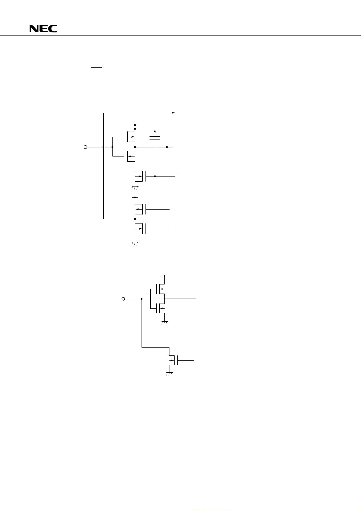
1.2 EQUIVALENT CIRCUITS OF THE PINS
P0A (P0A3/SO, P0A2/SCK)
P0B (P0B
P1B (P1B
P1C (P1C
1, P0B0/SI)
3, P1B2, P1B1, P1B0)
3/ADC1, P1C2, P1C1)
V
DD
µ
PD17062
A/D converter (only for P1C/ADC)
RESET signal (except for P1C)
Read instruction (only for P1C)
V
DD
P0A (P0A1/SCL, P0A0/SDA)
(I/O)
14
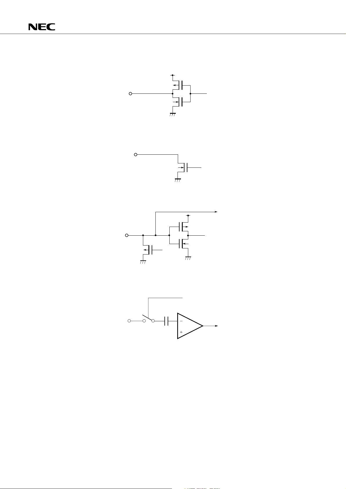
P0C (P0C3, P0C2, P0C1, P0C0)
RED, GREEN, BLUE, BLANK, PSC
PWM (PWM3, PWM2, PWM1, PWM0)
P1A (P1A
P0D (P0D3/ADC5, P0D2/ADC4, P0D1/ADC3, P0D0/ADC2)
3, P1A2, P1A1, P1A0)
(Output)
(Output)
µ
PD17062
ADC0
A/D Converter
(Input)
High on-state
resistance
A/D converter selection signal
15
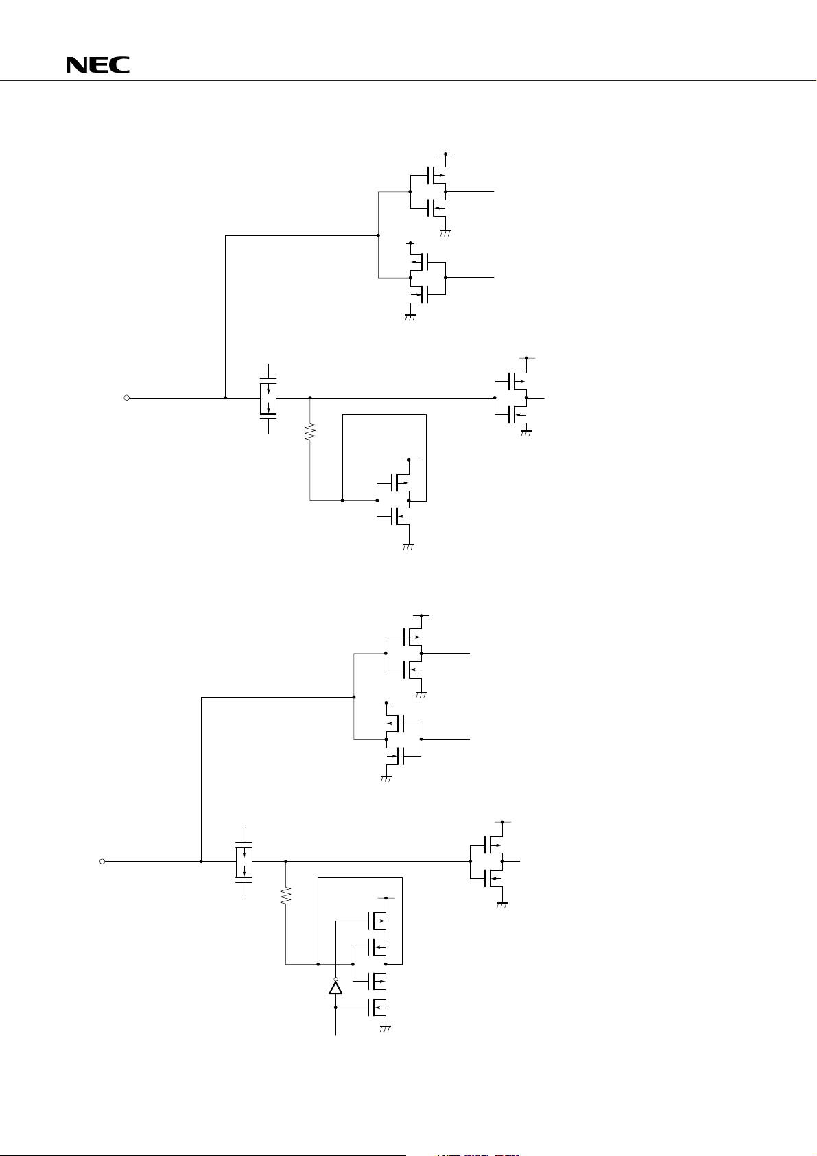
P0B3/HSCNT
Port
µ
PD17062
P0B2/TMIN
P-ch
N-ch
Port
Horizontal synchronizing
signal counter
16
P-ch
Timer/counter
N-ch
HSYNC, VSYNC, INTNC, CE
XOUT, XIN
(Hysteresis input)
µ
PD17062
EO
VCO
X
IN
X
OUT
(Input)
17
µ
PD17062
2. PROGRAM MEMORY (ROM)
Program memory stores the program to be executed by the CPU, as well as predetermined constant data.
2.1 CONFIGURATION OF PROGRAM MEMORY
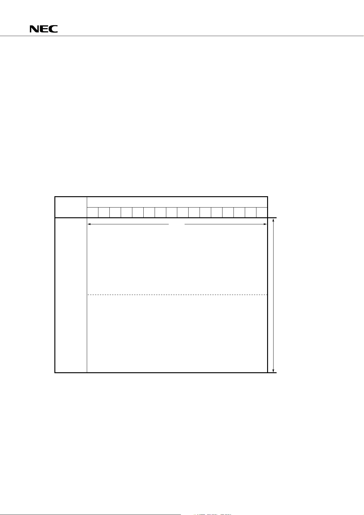
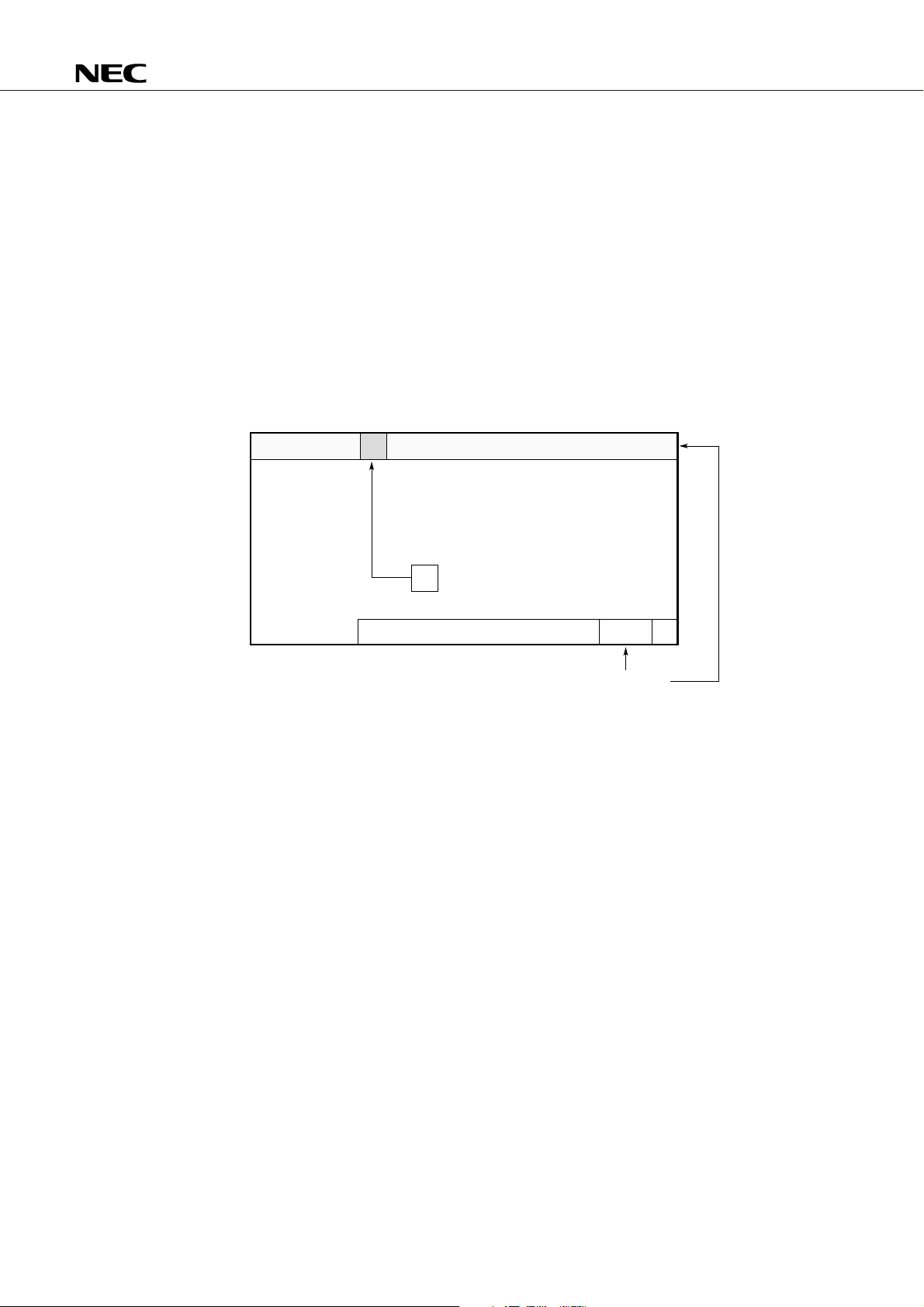
Fig. 2-1 shows the configuration of program memory.
As shown in Fig. 2-1, the capacity of the program memory is 8K bytes (3968 × 16 bits).
Locations in program memory are addressed in units of 16 bits. The total address range is from 0000H
to 0F7FH. Memory is divided into pages. The range of page 0 is from 0000H to 07FFH, while that of page
1 is from 0800H to 0F7FH.
The range from 0800H to 0F7FH can be used as the CROM (character ROM) area in which the display patterns
for the IDC are stored. If this area is not used as CROM, it can be used as a program area.
The range from 0000H to 00FFH is a table reference area. The area is used by the JMP @AR, CALL @AR,
MOVT, PUSH, and POP instructions.
Fig. 2-1 Configuration of Program Memory
Address
0000H
07FFH
0800H
0F7FH
Program memory (ROM)
15 b14 b13 b12 b11 b10 b9 b8 b7 b6 b5 b4 b3 b2 b1 b0
b
16 bits
Page 0
Page 1 (area that can be used as CROM)
3968 steps
18

µ
PD17062
2.2 FUNCTIONS OF PROGRAM MEMORY
Program memory has two basic functions:
(1) Program storage
(2) Constant data storage
A program is a set of instructions that control the CPU (Central Processing Unit: Device that actually
controls the microcontroller). The CPU executes processing sequentially according to the instructions coded
in the program. The CPU sequentially reads instructions from the program stored in program memory and
executes processing according to each instruction.
Each instruction is one word, or 16 bits in length. A single instruction can thus be stored at a single address
in program memory.
Constant data is predetermined data such as a display pattern. Constant data is read from program memory
into a data buffer (DBF) in data memory (RAM) upon execution of the specialized MOVT instruction. This
reading of constant data from memory is called table referencing.
Program memory is read-only storage that cannot be rewritten by the execution of an instruction. In this
document, program memory and ROM (read-only memory) are synonymous.
2.3 PROGRAM FLOW
A program stored in program memory is usually executed one address at a time starting from address
0000H. If another program is to be executed upon some condition being satisfied, the program flow must
be branched. To achieve this, the branch instruction (BR) is used.
If a single program is executed a number of times, the efficiency of the program memory is reduced. This
problem can be solved by storing that program at a given location and calling it using the specialized CALL
instruction. Such a program is called a subroutine while the usual program is called a main routine.
If a program is executed upon some condition being satisfied, independently of the current program flow,
the interrupt function is used. If a predetermined condition is satisfied, the interrupt function transfers control
to a specified address (vector address) irrespective of the current program flow.
These program flows are controlled by the program counter (PC), which specifies program memory
addresses.
19

µ
PD17062
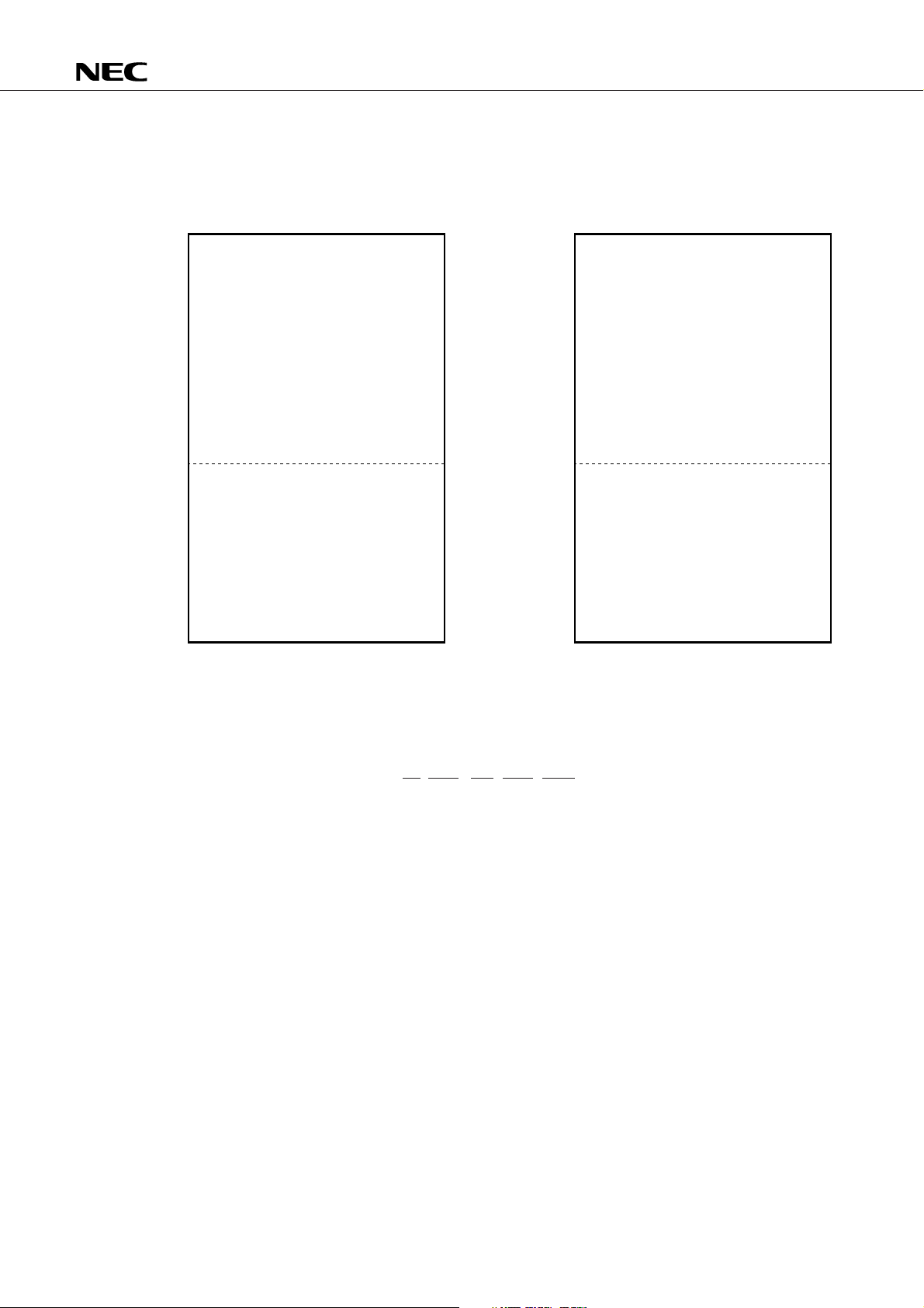
2.4 BRANCHING A PROGRAM
A program is branched by execution of the branch instruction (BR).
Fig. 2-2 illustrates the operation of the branch instruction.
Branch instructions (BR) are divided into two types. Direct branch instructions (BR addr) transfer control
to a program memory address (addr) directly specified in its operand. Indirect branch instructions (BR @AR)
transfer control to a program memory address specified in an address register (AR), described below.
See also Chapter 3.
2.4.1 Direct Branch
A direct branch instruction uses the least significant bit of the operation code and the 11 bits of its operand,
12 bits in total, to specify the destination program memory address. The destination of the direct branch
instruction can be any address in program memory between 0000H and 0F7FH.
2.4.2 Indirect Branch
The indirect branch instruction uses the eight-bit data of an address register to specify the destination
address. The destination of the indirect branch instruction is limited to addresses between 0000H and 00FFH.
See Section 8.1.
20
µ
PD17062
Fig. 2-2 Operation of Branch Instruction and Machine Code
(a) Direct branch (BR addr) (b) Indirect branch (BR @AR)
Address Program memory
0000H
0500H
07FFH
0800H
0900H
0F7FH
Label: Instruction (Machine code)
BR AAA (0C500)
BR BBB (0D100)
AAA:
Page 0
BR AAA (0C500)
BBB:
BR BBB (0D100)
Page 1
Address Program memory
0000H
0010H
0085H
0500H
07FFH
0800H
0F7FH
Label: Instruction (Machine code)
MOV AR0, #5H
MOV AR1, #8H
BR
@AR
Page 0
MOV AR0, #0H
MOV AR1, #1H
@AR
BR
Page 1
Remark The machine code (16 bits) of the 17K series consists of five blocks, of one bit, four bits, three bits,
four bits, and four bits. In this document, machine code is represented in these blocks so that
it can be easily understood.
Example Machine code 0C500 → 0 1100 101 0000 0000
14 3 4 4
2.4.3 Notes on Debugging
Direct branch instructions to page 0 (addresses 0000H to 07FFH) and page 1 (addresses 0800H to 0F7FH)
use different operation codes, as shown in Fig. 2-2.
The operation codes of the direct branch instructions to page 0 and page 1 are 0CH, and 0DH, respectively.
The difference arises because the direct branch instruction uses the addr operand, which is only 11 bits
long, together with the least significant bit of the operation code, to specify the branch destination address.
When assembling a program, the 17K series assembler (AS17K) references a jump destination identified
by a label and automatically converts the that instruction.
If the program is patched during debugging, the programmer must determine whether the branch
destination is on page 0 or page 1 and convert the instruction into operation code 0CH or 0DH.
If address BBB in (a) of Fig. 2-2 is patched from 0900H to 0910H, for example, the machine code of the BR
BBB instruction must be changed to 0D110.
21

µ
PD17062
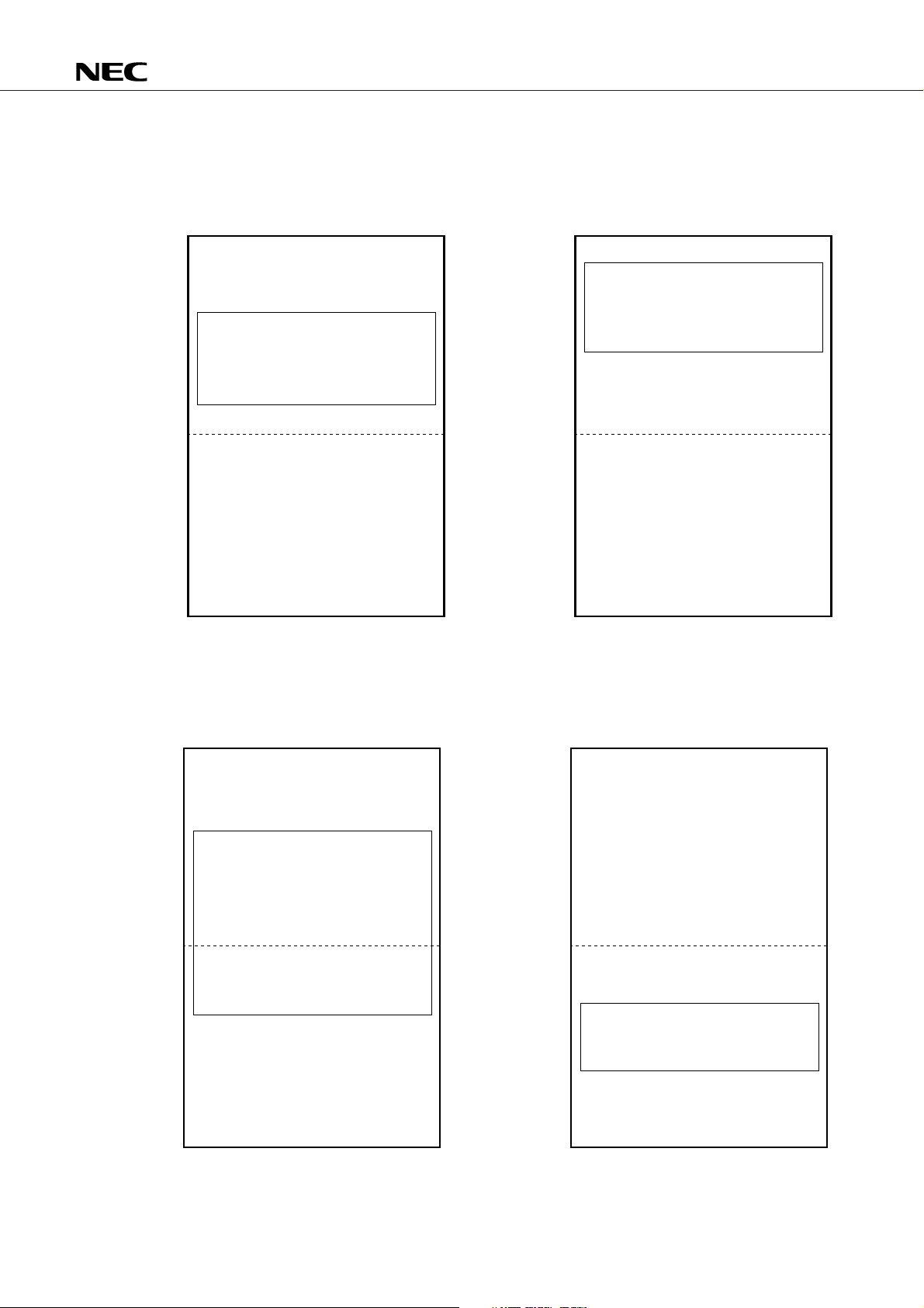
2.5 SUBROUTINE
If a subroutine is executed, the specialized subroutine call instruction (CALL) and subroutine return
instruction (RET, RETSK) are used.
Fig. 2-3 illustrates the operation of subroutine call.
Subroutine call instructions are divided into two types. The direct subroutine call instruction (CALL addr)
calls the program memory address (addr) specified in its operand. The indirect subroutine call instruction
(CALL @AR) calls the program memory address specified in an address register.
The RET or RETSK instruction is used to return control from a subroutine. The RET or RETSK instruction
returns control to a program memory address next to the address at which the subroutine call instruction
(CALL) was executed. Upon execution of the RETSK instruction, the first instruction after the return is executed
as a no-operation instruction (NOP).
See also Chapter 3.
2.5.1 Direct Subroutine Call
The direct subroutine call instruction uses 11 bits of its operand to specify the program memory address
to be called. If the direct subroutine call instruction is used, the destination, or the first address of the
subroutine to be called, must be page 0 (addresses 0000H to 07FFH). The instruction cannot call a subroutine
whose first address is in page 1 (addresses 0800H to 0F7FH).
The subroutine return instruction (RET, RETSK) can be in page 1. The CALL instruction can be in page 0
or page 1.
Examples 1. When the subroutine return instruction is in page 0
When the first address of the subroutine is in page 0, as shown in Fig. 2-4, the return address
and return instruction can be in page 0 or page 1. When only the first address of the subroutine
is in page 0, the CALL instruction can be used in either page. If the first address of the
subroutine cannot be placed in page 0 because of programming restrictions, the method
shown in example 2 can be used.
2. When the first address of the subroutine is in page 1
The branch instruction (BR) is placed in page 0, as shown in Fig. 2-4, and the desired
subroutine (SUB1) is called via the BR instruction.
2.5.2 Indirect Subroutine Call
The indirect subroutine call instruction (CALL @AR) uses the 8-bit data in an address register (AR) to specify
the address of a subroutine to be called. The instruction can call a subroutine from a program memory address
between 0000H and 00FFH.
See Section 8.1.
22
µ
PD17062
Fig. 2-3 Operation of Subroutine Call Instruction
(a) Direct subroutine call (CALL addr) (b) Indirect subroutine call (CALL @AR)
Address Program memory
0000H
0500H SUB1:
07FFH
0800H
0F7FH
Label: Label:
Instruction
CALL SUB1
RET
Page 0
CALL SUB1
Page 1
Fig. 2-4 Sample Uses of Subroutine Call Instruction
Address Program memory
0000H
0010H
0085H
07FFH
0800H
0F7FH
SUB2:
SUB3:
Instruction
RET
MOV AR0, #0H
MOV AR1, #1H
CALL @AR
Page 0
MOV AR0, #5H
MOV AR1, #8H
CALL @AR
Page 1
(a) If the subroutine return instruction is in page 1 (b) If the first address of the subroutine is in page 1
Address Program memory
0000H
0500H SUB1:
07FFH
0800H
0F7FH
Instruction
CALL SUB1
Page 0
RET
CALL SUB1
Page 1
Address Program memory
0000HLabel: Label:
SUB1:BR SUB2
07FFH
0800H
0890H SUB2:
0F7FH
Instruction
CALL SUB1
Page 0
RET
CALL SUB1
Page 1
23
µ
PD17062
2.6 TABLE REFERENCE
The table reference instruction is used to reference the constant data in program memory. If the MOVT
DBF, @AR instruction is executed, data at the program memory address specified in an address register is
placed in a data buffer (DBF).
Because each data item in program memory consists of 16 bits, the constant data placed in the data buffer
by the MOVT instruction also consists of 16 bits (four words). Because the address register consists of eight
bits, the MOVT instruction can reference a program memory address between 0000H and 00FFH.
When table referencing is executed, a single stack is used.
See Sections 8.1 and 10.3.
2.7 NOTES ON USING THE BRANCH INSTRUCTION AND SUBROUTINE CALL INSTRUCTION
The 17K series assembler (AS17K) detects an error if a program memory address (numeric address) is
directly specified in the operand of the branch instruction (BR) or subroutine call instruction (CALL).
The assembler provides this function to minimize the number of bugs arising from program modification.
Examples 1. Instruction causing an error
;
#
BR 0005H ; The assembler detects the error.
;
$
CALL 00F0H ;
2. Instruction causing no error
;
%
LOOP1: ; The BR or CALL instruction is executed for a label used in the
BR LOOP1 ; program.
;
&
SUB1: ;
CALL SUB1 ;
;
(
LOOP2 LAB 0005H ; As a label type, 0005H is assigned to LOOP2.
BR LOOP2 ;
;
)
BR. LD. 0005H ; The numeric value of the operand is converted to a label type.
; It is recommended that this method not be used to reduce
; the number of bugs.
For details, refer to the AS17K User’s Manual.
24
µ
PD17062
3. PROGRAM COUNTER (PC)
The program counter addresses program memory or a program. It is a 12-bit binary counter.
Fig. 3-1 Program Counter
PC11 PC9PC10 PC8 PC6PC7 PC5 PC3PC4 PC2 PC0PC1
12 bits
Normally, the program counter is incremented by 1 each time an instruction is executed. When a branch
instruction or a subroutine call instruction is executed, however, the address specified in the operand field
is loaded into the program counter. If a skip instruction has been executed, the address of the instruction
following the skip instruction is specified, regardless of the contents of the skip instruction. If the specified
address contains a skip condition, the instruction following the skip instruction is regarded as being a NOP
instruction. That is, the NOP instruction is executed, and the address of the next instruction is specified.
If an interrupt request is accepted, one of addresses 1 to 4 (depending on the cause of the interrupt) is loaded
into the PC.
If a power-on reset or a CE reset is performed, the program counter is reset to address 0.
Table 3-1 Vector Addresses upon Interrupt Occurrence
Priority Interrupt cause Vector address
1 INT
2 Internal timer 3H
3VSYNC pin 2H
4 Serial interface 1H
NC pin 4H
25
µ
PD17062
4. STACK
The stack is a register used to save an address returned by a program or the contents of the system register,
described later, when a subroutine call occurs or an interrupt is accepted.
4.1 COMPONENTS
The stack consists of a stack pointer (SP), which is a 4-bit binary counter, six 13-bit address stack registers
(ASRs), and two 3-bit interrupt stack registers.
4.2 STACK POINTER (SP)
The stack pointer is located at address 01H in the register file, and specifies an address stack register. The
contents of the stack pointer are decremented by 1 whenever a push operation (CALL, MOVT, or PUSH
instruction or interrupt acceptance) is performed, or incremented by 1 whenever a pop operation (RET, RETSK,
RETI, MOVT, or POP instruction) is performed.
The high-order bit of the stack pointer is always set to 0. The stack pointer can indicate any of eight different
values, 0H to 7H. However, 6H and 7H are not assigned to the stack.
Fig. 4-1 Structure of Stack Pointer
MSB LSB
0 (SPb2) (SPb1) (SPb0)
Table 4-1 Behavior of Stack Pointer
Instruction Stack pointer value
CALL addr
CALL @AR
MOVT DBF, @AR SP – 1
PUSH AR
Interrupt acceptance
RET
RETSK
MOVT DBF, @AR SP + 1
POP AR
RETI
26
µ
PD17062
4.3 ADDRESS STACK REGISTERS (ASRs)
There are six address stack registers, each consisting of 13 bits. After a subroutine call instruction has been
executed or an interrupt request accepted, the contents of the address stack register will contain a value that
is equal to the contents of the program counter, plus one, or the return address. The contents of an address
stack register are loaded into the program counter by executing a return instruction, after which control returns
to the original program flow.
The address stack registers are used for both subroutine calls and interrupts. If two levels of the address
stack registers are used for interrupts, the remaining four levels can be used for subroutine calls.
If a MOVT instruction is executed, an address stack register is used temporarily.
Fig. 4-2 Structure of Address Stack Registers
Stack pointer value
0H
1H
2H
3H
4H
5H
ASR0
ASR1
ASR2
ASR3
ASR4
ASR5
4.4 INTERRUPT STACK REGISTERS
There are two interrupt stack registers, each consisting of three bits, as shown in Fig. 4-3.
If an interrupt is accepted, the value of the two bits of the bank register (BANK) and the value of the one
bit of the index-enable flag (IXE) in the system register (SYSREG), described later, are saved to an interrupt
stack register. Once an interrupt return instruction (RETI) has been executed, the contents of the interrupt
stack register are returned to the bank register and the index-enable flag of the system register.
Unlike the address stack registers, the interrupt stack registers contain no addresses specified by the stack
pointer. As shown in Fig. 4-4, data is saved to an interrupt stack pointer each time an interrupt is accepted,
the saved data being returned whenever an interrupt return instruction is executed. If accepted interrupts
consist of more than two levels, the first level of data is pushed out. Thus, it must be saved by the program.
If a power-on reset is performed, the contents of the interrupt stack registers become undefined. Even if
a CE reset is performed or a clock stop instruction is executed, however, the contents of the interrupt stack
registers remain as is.
27
Fig. 4-3 Structure of Interrupt Stack Registers
MSB LSB
µ
PD17062
0H
1H
Fig. 4-4 Behavior of Interrupt Stack Registers
Not defined B A Not definedA
Not defined A Not defined Not definedNot defined
BANKSK0
BANKSK1
IXESK0
IXESK1
RETIRETIInterrupt BInterrupt AVDD is applied.
28

µ
PD17062
5. DATA MEMORY (RAM)
Data memory is used to store data for operations and control. Simply by executing an appropriate
instruction, data can be written to and read from data memory at any time.
5.1 STRUCTURE OF DATA MEMORY
Fig. 5-1 shows the structure of data memory.
As shown in Fig. 5-1, data memory is divided into three units called banks. These three banks are called
BANK0, BANK1, and BANK2.
In each bank, data is assigned an address in units of four bits. The high-order three bits are called the row
address, while the low-order four bits are called the column address. For example, the data memory location
having row address 1H and column address AH is referred to as the data memory location having address
1AH. One address consists of four bits of memory. These four bits are called a nibble.
Data memory is divided into the blocks described in Sections 5.1.1 to 5.1.5, according to function.
29
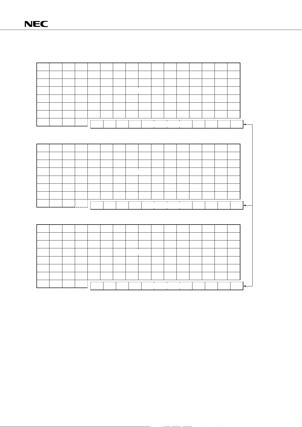
Fig. 5-1 Data Memory Structure
0123456789ABCDEF
0
1
2
3
BANK0
4
5
6
P0A
P0B
P0C
7
(4 bits)
(4 bits)
(4 bits)
P0D
(4 bits)
System register
0123456789ABCDEF
0
1
2
3
BANK1
4
5
6
P1A
P1B
P1C
7
(4 bits)
(4 bits)
(4 bits)
Fixed
at 0
System register
DBF3 DBF2 DBF1 DBF0
µ
PD17062
0123456789ABCDEF
0
1
2
3
BANK2
4
5
6
P0A
P0B
P0C
7
(4 bits)
(4 bits)
(4 bits)
P0D
(4 bits)
System register
The same register is allocated for each bank.
30

µ
PD17062
5.1.1 Structure of the System Register (SYSREG)
The system register consists of 12 nibbles, located at addresses 74H to 7FH in data memory. The system
register is allocated regardless of the bank. That is, the system register is always located at addresses 74H
to 7FH, regardless of the bank.
Fig. 5-2 shows the structure.
Fig. 5-2 Structure of the System Register
System register (SYSREG)
74H 75H 76H 77H 78H 79H 7AH 7BH 7CH 7DH 7EH 7FHAddress
Register
(symbol)
Address register
(AR)
Window
register
(WR)
Bank
register
(BANK)
Index register (IX)
Data memory row
address pointer
(MP)
General-purpose
register pointer
(RP)
status word
(PSWORD)
5.1.2 Structure of the Data Buffer (DBF)
The data buffer consists of four nibbles located at addresses 0CH to 0FH of BANK0 in data memory.
Fig. 5-3 shows the structure.
Fig. 5-3 Structure of the Data Buffer
Data buffer (DBF)
Address
Symbol
0CH
DBF3
0DH
DBF2
0EH
DBF1
0FH
DBF0
Program
31

µ
5.1.3 Structure of the General-Purpose Register (GR)
The general-purpose register consists of 12 nibbles, specified with an arbitrary row address, in data
memory.
An arbitrary row address is specified using the general-purpose register pointer in the system register.
Fig. 5-4 shows the structure.
Fig. 5-4 Structure of the General-Purpose Register (GR)
PD17062
Column address
0123456789ABCDEF
0
1
2
3
4
5
Row address
6
7
0
1
2
3
4
5
6
7
0
1
2
3
4
5
6
7
BANK0
SYSREG
BANK1
SYSREG
BANK2
SYSREG
General-purpose register
Area specifiable as general-purpose
register
Pointed to by general-purpose
register pointer (RP) in system
register.
The same register is allocated
for each bank.
32

µ
PD17062
5.1.4 Structure of Port Data Registers (port register)
The port registers consist of 12 nibbles at addresses 70H to 73H of the banks of data memory.
Fig. 5-5 shows the structure of the port registers.
As shown in Fig. 5-5, the same port registers are allocated in BANK0 and BANK2. Thus, the port registers
actually consist of eight nibbles.
Fig. 5-5 Structure of Port Registers
Port register
Address
70H 71H 72H 73H
BANK0
BANK2
Symbol
BANK1
5.1.5 Structure of General-Purpose Data Memory
General-purpose data memory consists of that part of memory other than the system register and the port
registers of data memory.
General-purpose data memory consists of a total of 336 words, with 112 words in each of BANK0 to BANK2.
5.1.6 Unmounted Data Memory
As shown in Fig. 5-6, nothing is assigned to bit 0 of address 72H in BANK1 of the port registers. For an
explanation of this address, see Section 5.3.2.
P0A P0B P0C P0D
P1A P1B P1C Fixed at 0
33

µ
PD17062
5.2 FUNCTIONS OF DATA MEMORY
Data memory can be used to perform, with one instruction, a four-bit operation, comparison, decision, or
transfer of the data in data memory and immediate data (arbitrary data) by executing one of the data memory
manipulation instructions listed in Table 5-1.
If the general-purpose register is used, a four-bit operation, comparison, or transfer between data memory
and the general-purpose register can be performed by a single instruction.
Examples are given below. See Chapters 6 and 7 for details.
Example 1. Operation on data in data memory
;
#
MOV 35H, #0001B ; Transfer (write) immediate data 0001B to data
; memory address 35H in the currently selected bank.
;
$
ADD 76H, #0001B ; Add immediate data 0001B to the contents of
; data memory address 76H in the currently selected ;bank.
In instructions # and $, the currently selected bank is specified in the bank register of the
system register. For an explanation of the bank register, see Chapter 8.
In $, the instruction is for addition to the contents of data memory address 76H. Address
76H is part of the system register. Because the system register always exists regardless of
the bank, the ADD instruction eventually adds 0001B to the contents of address 76H of the
system register, regardless of the bank.
Remark For explanation of how to code instructions, see Section 5.3.1.
Example 2. Operation between data memory and the general-purpose register
Assume that the general-purpose register is allocated to row address 1H of BANK0.
;
#
ADD 7H, 36H ; Add the contents of data memory address 36H in the
; currently selected bank to the contents of the
; general-purpose register location having column address
; 7H, or address 17H of BANK0.
;
$
LD 7H, 36H ; Transfer the contents of data memory address 36H to
; the general-purpose register location having column
; address 7H.
; In this instruction, the general-purpose register
; location is address 17H of BANK0.
The system register, data buffer, general-purpose register, and port registers can be manipulated in the
same way as data memory by using the data memory manipulation instructions.
Sections 5.2.1 to 5.2.4 describe the functions of these registers.
34

µ
PD17062
5.2.1 Function of System Register (SYSREG)
The system register is used to control the CPU.
For example, the bank register shown in Fig. 5-2 is used to specify a data memory bank, while the general-
purpose register pointer specifies the row address of the general-purpose register.
See Chapter 8 for details.
5.2.2 Function of General-Purpose Register (GR)
The general-purpose register can be used both to perform operations on the data in data memory and to
transfer data to and from data memory.
The bank and the row address for the general-purpose register are specified by the general-purpose register
µ
pointer in the system register. The general-purpose register pointer of the
For example, if the general-purpose register pointer is set to 0, 16 nibbles at row address 0 of BANK0, or
addresses 00H to 0FH of BANK0, are allocated as the general-purpose register.
Note that if the general-purpose register is used, transfer and arithmetic/logical instructions that involve
the general-purpose register and immediate data cannot be executed. That is, the execution of a transfer or
an arithmetic/logical instruction that involves the general-purpose register and immediate data requires that
the general-purpose register be treated as data memory.
For example, assume that row address 0H of BANK0 is allocated as the general-purpose register (i.e., the
value of the general-purpose register pointer is 0). In this case, if the currently selected bank is BANK0 (i.e.,
the value of the bank register is 0), executing ADD 00H, #1 increments by 1 the contents of address 00H of
BANK0, which is allocated as the general register. However, if the currently selected bank is BANK1 (i.e., the
value of the bank register is 1), executing ADD 00H, #1 increments by 1 the contents of address 00H of BANK1.
See Chapter 6 for details.
PD17062 always specifies BANK0.
5.2.3 Data Buffer (DBF)
The data buffer is used to store data to be transferred to a peripheral circuit, such as the reference voltage
setting data for an A/D converter. It is also used to store data transferred from a peripheral circuit, such as
input data for a serial interface.
See Chapter 10 for details.
5.2.4 General-Purpose Port Data Registers (port registers)
Port registers are used both to store output data for general-purpose I/O ports and to read input data. The
output of the pins assigned as an output port is determined by storing data into the port registers that
correspond to those pins. The input status of those pins assigned as an input port can be detected by reading
the contents of the port registers corresponding to those pins. Fig. 5-6 shows the correspondence between
the port registers and ports (pins).
See Chapter 15 for details.
35

Table 5-1 Data Memory Manipulation Instructions
Function Instruction
ADD
ADDC
SUB
SUBC
AND
OR
XOR
SKE
SKGE
SKLT
SKNE
MOV
LD
ST
SKT
SKF
Operation
Comparison
Transfer
Decision
Addition
Subtraction
Logical
operation
µ
PD17062
36
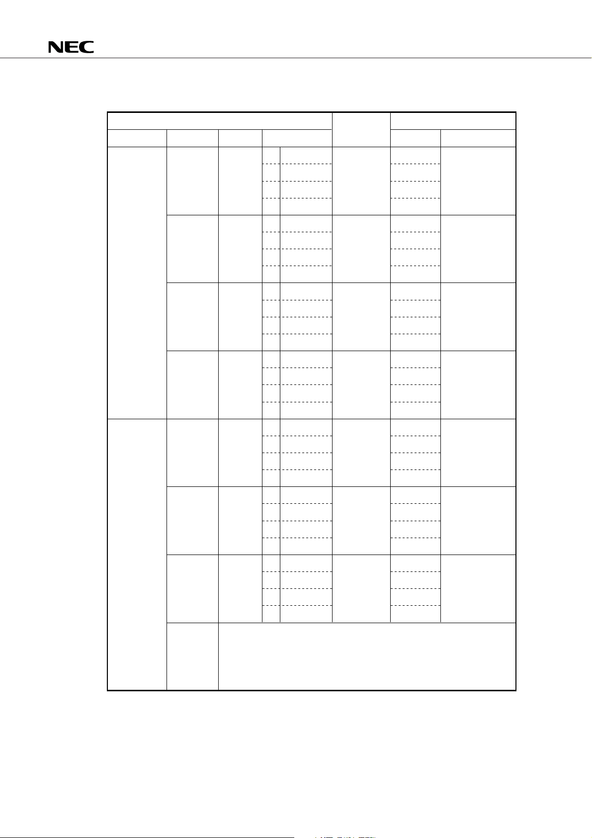
Fig. 5-6 Correspondence Between Port Registers and Ports (Pins)
µ
PD17062
BANK0
BANK2
General-purpose port data register
AddressBank Symbol Bit symbol
b
70H P0A
b2 P0A2
b
b
b
b2 P0B2
71H P0B
b
b
b
72H P0C
b2 P0C2
b
b
b
73H P0D
b2 P0D2
b
b
3 P0A3
1 P0A1
0 P0A0
3 P0B3
1 P0B1
0 P0B0
3 P0C3
1 P0C1
0 P0C0
3 P0D3
1 P0D1
0 P0D0
Corresponding
port
Port0A
Port0B
Port0C
Port0D
Pin
Symbol Input or output
3
P0A
P0A2
P0A1
Input and output
(bit I/O)
P0A0
P0B3
P0B2
P0B1
Input and output
(bit I/O)
P0B0
P0C3
P0C2
Output
P0C1
P0C0
P0D3
P0D2
Input
P0D1
P0D0
BANK1
70H P1A
71H P1B
72H P1C
73H Fixed at 0
b
3 P1A3
b2 P1A2
1 P1A1
b
0 P1A0
b
b3 P1B3
b2 P1B2
1 P1B1
b
0 P1B0
b
b3 P1C3
b2 P1C2
1 P1C1
b
0 P1C0
b
Port1A
Port1B
Port1C
P1A3
P1A2
P1A1
P1A0
P1B3
P1B2
P1B1
P1B0
P1C3
P1C2
P1C1
–
Output
Input and output
(bit I/O)
Input and output
(group I/O)
37

µ
PD17062
5.3 NOTES ON USING DATA MEMORY
5.3.1 Addressing Data Memory
If the 17K series assembler is being used and a numeric representing a data memory address is specified
directly in an operand of a data memory manipulation instruction, as shown in example 1, an error will occur.
This error occurs to facilitate the maintainability of programs and to reduce the number of causes of bugs
when a program is modified. In this data sheet, however, real-address notation is used in the sample programs
to make them easy to understand. When coding an actual program, refer to the assembler instruction manual.
Example 1.
Instructions that result in an error
;
#
MOV 2FH, #0001B ; Address 2FH is specified directly.
;
$
MOV 0.2FH, #0001B ; Address 2FH in BANK0 is specified directly.
Instructions that do not cause an error
;
%
M02F MEM 0.2FH ; Address 2FH of BANK0 is defined symbolically in
MOV M02F, #0001B ; M02F as a memory-type address.
;
&
MOV .MD.2FH, #0001B ; Address 2FH is converted into a memory-type
; address by using .MD.. However, the use of this type of
; instruction should be avoided to reduce the
; likelihood of bugs arising.
Using an assembler pseudo instruction, namely the MEM instruction (symbol definition pseudo instruc-
tion), symbolically define a data memory address in advance.
If a data memory address is defined symbolically, a data memory bank must also be specified, as shown
in example 2.
This data memory bank specification is used when a data memory map is automatically created in the
assembler.
Note that if a symbolically defined data memory address for BANK2 is used in the range of BANK1 in a
program, as shown in example 2, the operation is performed in BANK1 data memory.
38

Example 2.
µ
PD17062
M1
M2
M3
BANK1
MOV M1,
MOV M2,
MOV M3,
5.3.2 Notes on Using Unmounted Data Memory
As shown in Fig. 5-6, nothing is actually assigned to bit 0 (LSB) of address 72H of BANK1 of the port registers.
If a data memory manipulation instruction is executed for this address, the following operations are
performed:
(1) Device behavior
If a read instruction is executed, a 0 is read.
Executing a write instruction results in no change.
MEM
MEM
MEM
Bank Row address Column address
0.15H
1.15H
2.15H
#0000B
#0000B
#0000B
;
Symbol definition pseudo instruction
;
;
; Assembler built-in macro instruction BANK ← 1
M1, M2, and M3 are defined symbolically in # for different
;
banks, but are for BANK1 in this program. Thus, all of these
;
three instructions write 0s to data memory address 15H in BANK1.
;
(2) Assembler behavior
Normal assembly is performed.
No error occurs.
(3) Emulator (IE-17K) behavior
If a read instruction is executed, a 0 is read.
Executing a write instruction results in no change.
No error occurs.
39

µ
PD17062
6. GENERAL-PURPOSE REGISTER (GR)
The general-purpose register is allocated in data memory space, and is used to perform direct operations
on the data in data memory and to transfer data to and from data memory.
6.1 STRUCTURE OF THE GENERAL-PURPOSE REGISTER
Fig. 6-1 shows the structure of the general-purpose register.
As shown in Fig. 6-1, 16 words (16 words × 4 bits) having the same row address in data memory space can
be used as the general-purpose register.
The row address to be used as the general-purpose register can be specified using the general-purpose
register pointer of the system register. The general-purpose register consists of seven bits. However, the
high-order four bits are fixed to 0 so, within the data memory space, only row addresses 0H to 7H of BANK0
can be used as the general-purpose register.
See Section 8.6.
6.2 FUNCTION OF THE GENERAL-PURPOSE REGISTER
The general-purpose register can be used to perform an operation or to transfer data between itself and
data memory with the execution of a single instruction. The general-purpose register is allocated in data
memory space. This enables an operation or transfer to be performed between data memory locations by
the execution of a single instruction.
Like other data memory, the general-purpose register can be controlled using a data memory manipulation
instruction.
40
Row addresses 0H to 7H
of BANK0 can be freely
specified using the generalpurpose register pointer (RP).
Fig. 6-1 Structure of General-Purpose Register
Column address
0123456789ABCDEF
0
1
2
3
4
Row address
5
6
7
0
1
2
3
4
5
6
7
General-purpose register (16 words)
BANK0
System register
BANK1
System register
RP
µ
PD17062
General-purpose
register allocated
when RP = 010B.
The same system
register is viewed.
General-purpose register
pointer (RP)
Symbol
Address
Bit
Function
RPH RPL
7DH 7EH
b3 b2 b1 b0 b3 b2 b1 b0
0000b2b1b0B
(RP)
C
D
0
1
2
3
4
5
6
7
BANK2
System register
41
µ
PD17062
6.3 ADDRESS GENERATION FOR GENERAL-PURPOSE REGISTER AND DATA MEMORY IN INDIVIDUAL
INSTRUCTIONS
Table 6-1 lists the operation and transfer instructions that can be executed for the data in the general-
purpose register and data memory.
Consider the following instruction:
ADD r, m ((r) ← (r) + (m))
Upon executing this instruction, the address of the general-purpose register is generated from the value
of the general-purpose register pointer and the value specified in r, as shown in Table 6-2. Then, the contents
of the general-purpose register specified by the generated address of the general-purpose register are added
to the contents of the data memory location specified in m, the result being stored into the general-purpose
register.
The address of the general-purpose register is generated, as described above, for each of the instructions
listed in Table 6-1.
Table 6-1 Manipulation Instructions Executed between the General-Purpose Register and Data Memory
Instruction set Instruction Operation
Addition ADD r, m (r) ← (r) + (m)
ADDC r, m (r) ← (r) + (m) + CY
Subtraction SUB r, m (r) ← (r) – (m)
SUBC r, m (r) ← (r) – (m) – CY
Logical operation AND r, m (r) ← (r) ∧ (m)
OR r, m (r) ← (r) ∨ (m)
XOR r, m (r) ← (r) ∨
Transfer LD r, m (r) ← (m)
ST m, r (m) ← (r)
MOV @r, m if MPE = 1: (MP, (r)) ← (m)
if MPE = 0: (BANK, mR, (r)) ← (m)
MOV m, @r if MPE = 1: (m) ← (MP, (r))
if MPE = 0: (m) ← (BANK, mR, (r))
Shift RORC r Right shift, including a carry
−
(m)
Table 6-2 Address Generation for General-Purpose Register and Data Memory
Instruction Address
Bank Row address Column address
Generated address
42
ADD r, m
General-purpose register
address specified in r
Data memory address
specified in m
(0000B)
(BANK)
(00 × × B)
(RP) r
m
µ
PD17062
Example 1. When BANK0 is selected
AND RPL, #0001B ; RP ← 0000000B; The general-purpose register is allocated in row
; address 0H in BANK0.
ADD 04H, 56H ;
Executing the above instruction adds the contents of address 04H of BANK0, part of the general-purpose
register, to the contents of data memory address 56H, then stores the result into address 04H of the general-
purpose register. See Fig. 6-2.
Fig. 6-2 Execution of Instructions in Example 1
Column address
012 3456789ABCDEF
0
1
General-purpose register
2
3
4
Row address
5
6
7
ADD 04H, 56H
BANK0
M
System register
RP
0000000B
43

µ
PD17062
Example 2. When BANK0 is selected and MPE = 0 is specified
MOV 04H, #8 ; 04H ← 8
AND RPL, #0001B ; RP ← 0000000B; The general-purpose register is allocated in row
; address 0H in BANK0.
MOV @04H, 52H
Executing the above instruction transfers the contents of data memory address 52H to address 58H. The
MOV @r, m instruction is called an indirect transfer of the general-purpose register contents. In this
instruction, the contents of the general-purpose register address specified in r (8 in the above example) consist
of the column address of data memory, and the row address specified in m (5 in the above example) is the
row address of data memory. That is, the data memory address is 58H (see Fig. 6-3).
See Section 8.5 for an explanation of the indirect transfer of the general-purpose register contents.
Fig. 6-3 Execution of Instructions in Example 2
Column address
012 3456789ABCDEF
0
1
8
General-purpose register
Example 3.
2
3
4
Row address
5
6
7
M
MOV
@ 04H, 56H
System register
BANK0
RP
AND RPL, #0000B ; RP ← 0000000B; The general-purpose register is allocated in row
; address 0H of BANK0.
MOV BANK, #0010B ; BANK2
LD 01H, 31H
LD 02H, 32H
LD 03H, 33H
LD 04H, 34H
OR RPL, #1000B ; RP ← 0000100B; The general-purpose register is allocated in row
; address 4H of BANK0.
LD 05H, 45H
LD 06H, 46H
LD 07H, 47H
LD 08H, 48H
44

µ
PD17062
Example 3 shows a program that transfers eight words of data from BANK2 to BANK0 data memory in units
of four words, as shown in Fig. 6-4. If the general-purpose register is allocated in a fixed row address, for
example, only in row address 0 of BANK0, instructions are needed to transfer all of the eight words to the
register and then store them into data memory. In contrast, if the row address of the general-purpose register
is changed using the general-purpose register pointer as shown in example 3, the operation can be completed
simply by executing a storage instruction.
Fig. 6-4 Execution of Instructions in Example 3
Column address
012 3456789ABCDEF
0
1
2
3
BANK0
RP = 0000000B
4
Row address
5
6
7
0
1
2
3
4
5
6
7
0
1
2
3
System register
System register
RP = 0000100B
RP
BANK1
BANK2
4
5
6
7
System register
45

µ
PD17062
6.4 NOTES ON USING THE GENERAL-PURPOSE REGISTER
This section provides notes on using the general-purpose register, referring to the following example:
Example
AND RPL, #000B ; RP ← 0000010B
OR RPL, #0100B ;
MOV BANK, #0000B ; BANK0
LD 04H, 32H
Executing the above instructions loads the contents of address 32H of BANK0 data memory into address
24H in the general-purpose register of BANK0.
In the above example, the general-purpose register is allocated in row address 2H of BANK0, so that the
address of the general-purpose register specified in r in instruction LD r, m is address 24H of BANK0. The
data memory address specified in m is address 32H of BANK0. (See Fig. 6-5.)
Note that it is necessary to code an actual data memory address, for example, 24H, as the value specified
in r when using the assembler. In this case, only the low-order four bits are needed as the value for r, so the
assembler ignores value 2H, which is a row address. Thus, executing instruction LD 24H, 32H produces the
same result as executing the instruction in the above example.
If, when using the assembler, the address of the general-purpose register is specified directly in an operand
of an instruction, as shown below, an error occurs.
Instruction that causes an error
LD 04H, 32H ; The address of the general-purpose register is coded as 04.
Most commonly used method
R1 MEM 0.04H ;
M1 MEM 0.32H ; # R1 and M1 are defined as memory-type addresses, and are
LD R1, M1 ; assigned addresses 04H and 32H of BANK0, respectively.
Executing the following instructions produces the same result as executing the instructions in # because
R1 and R2 are assigned the same column address.
R2 MEM 0.34H
M1 MEM 0.32H
LD R2, M1
46
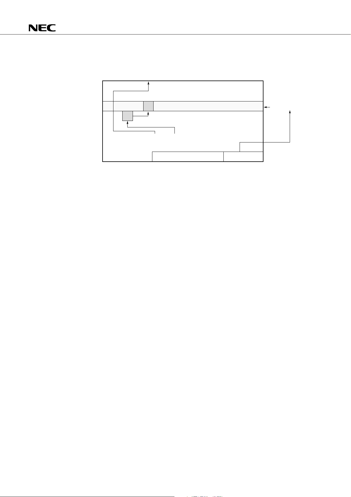
Fig. 6-5 Execution of the Above Example
Column address
012 3456789ABCDEF
0
1
µ
PD17062
2
3
4
Row address
5
6
7
LD 04H, 32H
General-purpose register
BANK0
System register
RP = 0000010B
RP
Also, note the following when the general-purpose register is being used. No arithmetic/logical instructions
are provided for the general-purpose register and immediate data. That is, the execution of an arithmetic/
logical instruction that involves data memory allocated as the general-purpose register and immediate data
requires that the data memory be treated as data memory rather than the general-purpose register.
47

µ
7. ARITHMETIC LOGIC UNIT (ALU) BLOCK
7.1 OVERVIEW
Fig. 7-1 is an overview of the ALU block.
As shown in Fig. 7-1, the ALU block consists of the ALU, temporary storage registers A and B, program
status word, decimal conversion circuit, and data memory address controller.
The ALU performs arithmetic and logic operations on the 4-bit data in the data memory and performs
discrimination, comparison, rotation, and transfer.
Fig. 7-1 Overview of the ALU Block
Data bus
PD17062
Address
controller
Data memory
Temporary
register A
Indexing memory
pointer
storage
Temporary
storage
register B
Program status
word
Detecting a carry,
borrow, or zero
Setting decimal
calculation or result
storage
ALU
• Arithmetic operation
• Logic operation
• Bit discrimination
• Comparative
discrimination
• Rotation
• Transfer
Decimal conversion
48

µ
PD17062
7.2 CONFIGURATION AND FUNCTIONS OF THE COMPONENTS OF THE ALU BLOCK
7.2.1 ALU
In response to a programmed instruction, the ALU performs 4-bit arithmetic or logic processing, bit
discrimination, comparative discrimination, rotation, or transfer.
7.2.2 Temporary Storage Registers A and B
Temporary storage registers A and B temporarily hold the 4-bit data.
These registers are automatically used when an instruction is executed. They cannot be controlled by a
program.
7.2.3 Program Status Word
A program status word controls the operation of the ALU and holds the status of the ALU.
For details of the program status word, see Section 8.7.
7.2.4 Decimal Conversion Circuit
If the BCD flag of the program status word is set to 1 when an arithmetic operation is executed, the decimal
conversion circuit converts the results of the arithmetic operation to a decimal number.
7.2.5 Address Controller
The address controller specifies an address in data memory.
At the same time, the circuit also controls address modification by the index register or data memory row
address pointer.
7.3 ALU OPERATIONS
Table 7-1 lists the operations performed by the ALU when instructions are executed.
Table 7-2 shows the data memory address modification by the index register and data memory row address
pointer.
Table 7-3 lists the converted decimal data used in decimal operations.
49

Table 7-1 ALU Operations
µ
PD17062
Instruction
ALU function
ADD
AdditionSubtractionLogic operation
ADDC
SUB
SUBC
OR
AND
XOR
SKT
nation
SKF
Discrimi-
SKE
SKNE
SKGE
ComparisonTransferRotation
SKLT
r, m
m, #n4
r, m
m, #n4
r, m
m, #n4
r, m
m, #n4
r, m
m, #n4
r, m
m, #n4
r, m
m, #n4
m, #n
m, #n
m, #n4
m, #n4
m, #n4
m, #n4
Value
of the
BCD flag
Optional
(hold)
Optional
(hold)
Optional
(hold)
Value
of the
CMP flag
00
01
10
11
Optional
(hold)
Optional
(reset)
Optional
(hold)
Operation difference due to program status word (PSWORD)
Operation
Operation
Binary operation
The result is stored.
Binary operation
The result is not
stored.
Decimal operation
The result is stored.
Decimal operation
The result is not
stored.
Not changed
Not changed
Not changed
of the
CY flag
Set by a
carry or
borrow.
Otherwise,
the flag
is reset.
Retains the
previous
state.
Retains the
previous
state.
Retains the
previous
state.
Operation of the Z flag Index
Set if the operation result is
0000B. Otherwise, the flag is
reset.
Retains the status if the
operation result is 0000B.
Otherwise, the flag is reset.
Set if the operation result is
0000B. Otherwise, the flag is
reset.
Retains the status if the
operation result is 0000B.
Otherwise, the flag is reset.
Retains the previous state.
Retains the previous state.
Retains the previous state.
Address modification
Memory
pointer
Provided
Provided
Provided
Provided
Not
provided
Not
provided
Not
provided
Not
provided
50
LD
ST
MOV
RORC r
r, m
m, r
m, #n4
@r, m
m, @r
Optional
(hold)
Optional
(hold)
Optional
(hold)
Optional
(hold)
Not changed
Not changed
Retains the
previous
state.
Value of b0 of
the generalpurpose
register
Retains the previous state.
Retains the previous state.
Provided
Not
provided
Not
provided
Provided
Not
provided

µ
PD17062
Table 7-2 Modification of the Data Memory Address and Indirect Transfer Address by the Index Register
and Data Memory Row Address Pointer
IXE MPE
00
01
10
11
General-purpose register address
b3 b2 b1 b0 b2 b1 b0 b3 b2 b1 b0 b3 b2 b1 b0 b2 b1 b0 b3 b2 b1 b0 b3 b2 b1 b0 b2 b1 b0 b3 b2 b1 b0
specified with r
Bank
Row
address
RP r BANK m BANK m
Same as
above
Same as
above
Same as
above
Column
address
Data memory address specified with m
Bank
BANK m BANK
BANK : Bank register
IX : Index register
IXE : Index enable flag
IXH : Bits 10 to 8 of the index register
IXM : Bits 7 to 4 of the index register
IXL : Bits 3 to 0 of the index register
m : Data memory address specified with m
mR : Data memory row address (high order)
m
C : Data memory column address (low order)
MP : Data memory row address pointer
MPE : Memory pointer enable flag
r : General-purpose register column address
RP : General-purpose register pointer
(×) : Contents addressed by ×
Row
address
Same as
above
Logical OR
Same as
above
R and mC
Column
address
Indirect transfer address specified with @r
Bank
Logical OR
IXH, IXMIX
Row
address
R (r)
m
R
Column
address
(r)MP
(r)
(r)MP
51

Table 7-3 Converted Decimal Data
µ
PD17062
Operation
result
10 0 1010B 1 0000B
11 0 1011B 1 0001B
12 0 1100B 1 0010B
13 0 1101B 1 0011B
14 0 1110B 1 0100B
15 0 1111B 1 0101B
16 1 0000B 1 0110B
17 1 0001B 1 0111B
18 1 0010B 1 1000B
19 1 0011B 1 1001B
20 1 0100B 1 1110B
21 1 0101B 1 1111B
22 1 0110B 1 1100B
23 1 0111B 1 1101B
24 1 1000B 1 1110B
25 1 1001B 1 1111B
26 1 1010B 1 1100B
27 1 1011B 1 1101B
28 1 1100B 1 1010B
29 1 1101B 1 1011B
30 1 1110B 1 1100B
31 1 1111B 1 1101B
Hexadecimal addi-
tion
CY CY
Operation
result
0 0 0000B 0 0000B
1 0 0001B 0 0001B
2 0 0010B 0 0010B
3 0 0011B 0 0011B
4 0 0100B 0 0100B
5 0 0101B 0 0101B
6 0 0110B 0 0110B
7 0 0111B 0 0111B
8 0 1000B 0 1000B
9 0 1001B 0 1001B
Decimal addition
Operation
result
Operation
result
Hexadecimal subtrac-
0 0 0000B 0 0000B
1 0 0001B 0 0001B
2 0 0010B 0 0010B
3 0 0011B 0 0011B
4 0 0100B 0 0100B
5 0 0101B 0 0101B
6 0 0110B 0 0110B
7 0 0111B 0 0111B
8 0 1000B 0 1000B
9 0 1001B 0 1001B
10 0 1010B 1 1100B
11 0 1011B 1 1101B
12 0 1100B 1 1110B
13 0 1101B 1 1111B
14 0 1110B 1 1100B
15 0 1111B 1 1101B
–16 1 0000B 1 1110B
–15 1 0001B 1 1111B
–14 1 0010B 1 1100B
–13 1 0011B 1 1101B
–12 1 0100B 1 1110B
–11 1 0101B 1 1111B
–10 1 0110B 1 0000B
–9 1 0111B 1 0001B
–8 1 1000B 1 0010B
–7 1 1001B 1 0011B
–6 1 1010B 1 0100B
–5 1 1011B 1 0101B
–4 1 1100B 1 0110B
–3 1 1101B 1 0111B
–2 1 1110B 1 1000B
–1 1 1111B 1 1001B
tion
CY CY
Operation
result
Decimal subtraction
Operation
result
Remark Correct decimal conversion is not possible in the shaded area.
52

µ
PD17062
7.4 NOTES ON USING THE ALU
7.4.1 Notes on Using the Program Status Word for Operations
After an arithmetic operation has been performed on the program status word, the operation result is held
in the program status word.
The CY and Z flags of the program status word are usually set or reset according to the result of the
arithmetic operation. If the arithmetic operation is performed on the program status word itself, the result
of the operation is stored and a carry, borrow, or zero cannot be discriminated.
If the CMP flag is set, the result of the arithmetic operation is not stored and the CY and Z flags are set or
reset as usual.
7.4.2 Notes on Performing Decimal Operations
A decimal operation can be carried out only when the operation result is within the following ranges:
(1) The result of addition is between 0 and 19 in decimal.
(2) The result of subtraction is between 0 and 9 or –10 and –1 in decimal.
If a decimal operation exceeding the above ranges is performed, the CY flag is set, resulting in a value
greater than or equal to 1010B (0AH).
53

µ
PD17062
8. SYSTEM REGISTER (SYSREG)
“System register” is the generic name for those registers directly related to CPU control. System registers
are allocated at addresses 74H-7FH in data memory and can be referenced regardless of the bank specification.
The system register types are as follows:
Address register
Window register
Bank register
Memory pointer enable flag
Index register
Data memory row address pointer
General-purpose register pointer
Program status word
Fig. 8-1 Configuration of System Register
Address
Register
Symbol
Bit
Data
74H 75H 76H 77H 78H 79H 7AH 7BH 7CH 7DH 7EH 7FH
System register
Index register
Address register
(AR)
AR3 AR2 AR1 AR0 WR BANK
b3 b2 b1 b0 b3 b2 b1 b0 b3 b2 b1 b0 b3 b2 b1 b0 b3 b2 b1 b0 b3 b2 b1 b0 b3 b2 b1 b0 b3 b2 b1 b0 b3 b2 b1 b0 b3 b2 b1 b0 b3 b2 b1 b0 b3 b2 b1 b0
00000000 00 P0000 0000
Window
register
(WR)
Bank
register
(BANK)
Data memory
row address
IXH IXM
MPH MPL
M
E
(IX)
pointer
(MP)
IXL RPH RPL PSW
(IX)
(MP)
Generalpurpose
register
pointer
(RP)
Program
status
word
(PSWORD)
B
C
CYZI
C
M
D
P
X
E
54

µ
PD17062
8.1 ADDRESS REGISTER (AR)
The address register specifies a program memory address. It is located at addresses 74H-77H. The
instructions used to manipulate the address register are indirect branch instructions (BR @AR, CALL @AR),
the table reference instruction (MOVT), and stack manipulation instructions (PUSH, POP).
An indirect branch is a branch to the program memory address specified by the contents of the address
register. Indirect branch instructions include BR @AR and CALL @AR.
Table reference is the transfer of the contents of the program memory address specified by the address
register to the DBF of data memory (BANK0 0DH-0FH). This is done by executing a MOVT instruction.
Stacks are manipulated using the PUSH and POP instructions. The PUSH instruction stores the contents
of the address register in the stack specified by the current stack pointer, and decrements the contents of the
stack pointer by 1. The POP instruction increments the contents of the stack pointer by 1, and loads the contents
of the stack specified by the current stack pointer into the address register.
µ
AR3 and AR2 of
register is the 256 steps of 0000H-00FFH.
PD17062 are fixed at 0. Hence, the program address that can be specified by the address
Fig. 8-2 Configuration of Address Register
AR3
(74H)
b30b20b10b00b30b20b10b00b3 b2 b1 b0 b3 b2 b1 b0
AR15 (MSB) AR0 (LSB)
8.2 WINDOW REGISTER (WR)
The window register is a 4-bit register, mapped to address 78H of the system register. It is used for data
transfer together with the register file (RF), described later in this manual. All data in each register of the
register file is manipulated via the window register.
Data transfer between the window register and the register file is achieved by execution of the exclusive
PEEK WR, rf and POKE rf, WR instructions.
AR2
(75H)
AR1
(76H)
AR0
(77H)
55

µ
PD17062
8.3 BANK REGISTER (BANK)
The bank register specifies a data memory bank.
The bank register contains BANK0 upon reset. The two high-order bits of address 79H are consistently set
to 0.
Data memory is classified into three banks by the bank register. When a data memory manipulation
instruction is executed, it acts on the data memory in the bank specified by the bank register.
For example, to manipulate BANK1 data memory with BANK0 set as the current bank, the bank must first
be switched to BANK1 in the bank register.
However, system registers allocated to addresses 74H-7FH of data memory are not confined to the concept
of banks. The same system registers exist at addresses 74H-7FH of all banks. Executing MOV 78H, #0 in BANK1
and MOV 78H, #0 in BANK2 both result in writing 0 to address 78H of the system register. Therefore, system
register manipulation is not constrained to the concept of banks.
When an interrupt is accepted, BANK is saved.
Table 8-1 Specification of Data Memory Bank
Bank request
(BANK)
b3 b2 b1 b0
0 0 0 0 BANK0
0 0 0 1 BANK1
0 0 1 0 BANK2
0 0 1 1 Not to be set
Data memory bank
8.4 MEMORY POINTER ENABLE FLAG (MPE)
The MPE specifies whether to specify the row address for execution of the MOV @r, M and MOV M, @r
instructions by the MPL, or to perform execution with the same address. When the MPE is set, the row address
is specified by the MPL. When the MPE is reset, the instruction is executed with same row address.
However, the address specified by the MPL is the row address of the currently specified bank.
56

µ
PD17062
8.5 INDEX REGISTER (IX) AND DATA MEMORY ROW ADDRESS POINTER (MP)
8.5.1 Configuration of Index Register and Data Memory Row Address Pointer
As shown in Fig. 8-1, the index register consists of 11 bits, including the three low-order bits, of 7AH (IXH)
of the system register, 7BH, and 7CH (IXM, IXL). The index register is used to indirectly specify a data memory
address.
The data memory row address pointer consists of 7 bits, including the three low-order bits of 7AH (MPH)
and 7BH (MPL).
This means that the seven high-order bits of the index register and data memory row address pointer are
shared.
The four high-order bits of the index register, i.e., the four high-order bits of the data memory row address
pointer (7AH b
2-b0, 7BH b3), of
µ
PD17062 are fixed at 0.
57

µ
PD17062
8.5.2 Functions of Index Register and Data Memory Row Address Pointer
When a data memory manipulation instruction is executed with the index enable flag (IXE) set to 1, the
index register ORs the data memory bank/address specified by the instruction and the contents of the index
register. Then, the index register executes the instruction in the data memory address indicated by the
operation result (in other words, the real address).
When a general-purpose register indirect transfer instruction (MOV @r, m and MOV m, @r) is executed
with the memory pointer enable flag set to 1, the data memory row address pointer executes the instruction,
regarding the indirect address bank specified by the general-purpose register and row address as being the
value of the data memory row address pointer.
Table 8-2 shows the modification of data memory and the indirect address by the index register and data
memory row address pointer.
All data memories are subject to modification by the index register and data memory row address pointer.
The following instructions are not subject to modification by the index register.
INC AR
INC IX
MOVT DBF, @AR
PUSH AR
POP AR
PEEK WR, rf
POKE rf, WR
GET DBF, P
PUT p, DBF
BR addr
BR @AR
RORC r
CALL addr
CALL @AR
RET
RETSK
RETI
EI
DI
STOP 0
HALT h
NOP
58
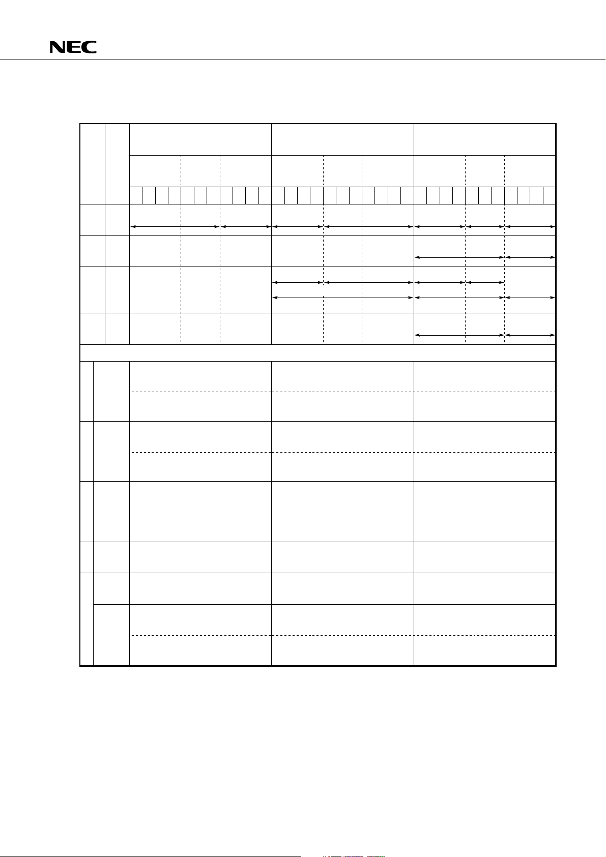
Table 8-2 Modification of Data Memory Address by Index Register and
Data Memory Row Address Pointer
µ
PD17062
IXE MPE
00
01
10
11
Address-modified instructions
ADD
ADDC
SUB
SUBC
Addition/subtractionLogical operation
AND
OR
XOR
General-purpose register address specified by r
R
Bank
b3b2b1b0b2b1b0b3b2b1b0b3b2b1b0b2b1b0b3b2b1b0b3b2b1b0b2b1b0b3b2b1b
Row
address
(RP) r (BANK) m (BANK) m
Same as
above
Same as
above
Same as
above
r
rm
Column
address
Data memory address specified by mMIndirect transfer address specified by @r
@R
Bank
BANK
Row
address
Same as
above
Logical
(IX)
Same as
above
m
m, #n4
m, #n4
OR
Column
address
m
Bank
(BANK) m
Logical OR
(IXH)
Row
address
R
(MP) (R)
R
(IXM)
(MP)
Column
address
(R)
(R)
(R)
0
SKE
SKGE
SKLT
Comparison
SKNE
SKT
SKF
nation
Discrimi-
LD
ST
MOV
Transfer
rm
@ r m
m, #n4
m, #n
m, #n4
Indirect transfer address
M ; Data memory address BANK ; Bank register
(M) ; Contents of data memory address (BANK) ; Contents of bank register
m ; Data memory address excluding banks IX ; Index register
m
R ; Data memory row address (IX) ; Contents of index register
R ; General-purpose register address IXH ; Bits b
(R) ; Contents of general-purpose register address IXM ; Bits b
r ; General-purpose register column address IXL ; Bits b
10-b8 of index register
7-b4 of index register
3-b0 of index register
RP ; General-purpose register pointer MP ; Data memory row address pointer
(RP) ; Contents of general-purpose register address (MP) ;
Contents of data memory row address pointer
59

µ
8.5.3 For MPE = 0 and IXE = 0 (Data Memory Not Modified)
As shown in Table 8-2, data memory addresses are not affected by the index register or data memory row
address pointer.
Example 1. When the row address of the general-purpose register is 0 for BANK0
ADD 03H, 11H
When the above instruction is executed, the contents of general-purpose register 03H and
data memory 11H are added and the result is stored in general-purpose register 03H. (See
Example 1 in Fig. 8-3).
Example 2. When the row address of the general-purpose register is 0 for BANK0
MOV 05H, #8 ; 05H ← 8
MOV @05H, 34H ; Register indirect transfer
When the above instruction is executed, the contents of the data memory at address 34H are
transferred to address 38H. This means that the MOV @ r, m instruction transfers the contents
of data memory m to the same row address (in the above case, 3) as m and the column address
(in the above case, 38H) specified by the contents (in the above case, 8) of general-purpose
register r. (See Example 2 in Fig. 8-3).
PD17062
Example 3. When the row address of the general-purpose register is 0 for BANK0
MOV 0BH, #0EH ; 0BH ← 0EH
MOV 34H @0BH ; Register indirect transfer
When the above instruction is executed, the contents of the data memory are transferred from
address 3EH to 34H. This means that the MOV m, @r instruction transfers the contents at
the same row address (in the above case, 3) as data memory m and at the column address
(in the above case, 3EH) specified by the contents (in the above case, 0EH) of general-purpose
register r to m (See Example 3 in Fig. 8-3). The (transfer) source and (transfer) destination
are exactly opposite to those in example 2.
60
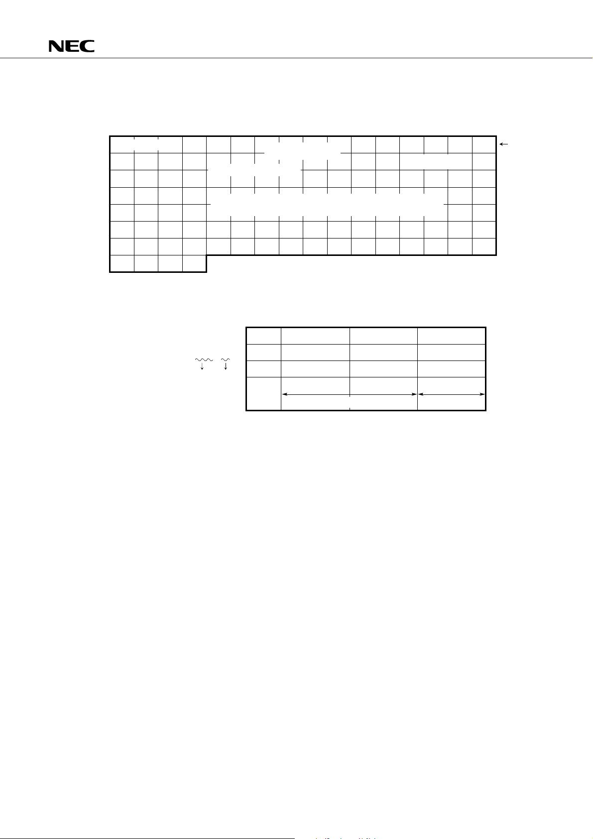
Fig. 8-3 Indirect Transfer of General-Purpose Register with MPE = 0 and IXE = 0
01 2 3 45 6 7 89 A B CD E F
Example 1. ADD03H,11H
0
1
2
3
4
Row address
5
6
7
Example 2. MOV @05H, 34H
Address generation of example 2
@ r, mMOV
05H 34H
µ
PD17062
Column address
8E
Specifies the destination
column address
Example 3. MOV 34H, @0BH
Bank Row address Column address
R
M
(@ r)
0
0
0
0
3
3
Same as M
Specifies the source
column address
5
4
8
Contents of R
Generalpurpose
register
61

µ
PD17062
8.5.4 For MPE = 1 and IXE = 0 (Diagonal Indirect Transfer)
As shown in Table 8-2, the bank and row address of the data memory address in the indirect side specified
by the general-purpose register are set to the value of the data memory row address pointer only when a
general-purpose register indirect transfer instruction is executed.
Example 1. When the row address of the general-purpose register is 0 for BANK0
MOV MPL, #0101B ; MP ← 00101B
MOV MPH, #1000B ; MPE ← 1
MOV 05H, #8 ; 05H ← 8
MOV @05H, 34H ; Register indirect transfer
When the above instruction is executed, the contents of the data memory at address 34H are
transferred to address 58H of data memory. This means that the MOV @r, m instruction at
MPE = 1 transfers the contents of data memory m to the data memory whose bank and row
addresses are the values of the data memory row address pointer (in the above example,
BANK0, row address 5) and whose column address is specified (in the above case, 58H of
BANK0) by general-purpose register r (in the above case, 8). (See Example 1 in Fig. 8-4.)
Compared to MPE = 0 (Example 2 in Section 8.5.3), the bank and row address of the data
memory address in the indirect side specified by the general-purpose register can be
specified by the data memory row address pointer (in Example 2 of Section 8.5.3, the bank
and row address in the indirect side are the same as those of m). Therefore, specifying MPE
= 1 enables general-purpose register diagonal indirect transfer to be performed.
Similarly, the MOV m, @r instruction becomes as shown in Example 2.
Example 2. When the row address of the general-purpose register is 0 for BANK0
MOV MPL, #0101B ; MP ← 00101B
MOV MPH, #1000B ; MPE ← 1
MOV 0BH, #0EH ; 0BH ← 0EH
MOV 3AH, @05H
(See Example 2 in Fig. 8-4.)
62

µ
Fig. 8-4 Indirect Transfer of General-Purpose Register with MPE = 1 and IXE = 0
PD17062
Generalpurpose
register
01 2 3 45 6 7 89 A B CD E F
0
1
2
3
4
5
6
7
Address generation of example 1
@ r, mMOV
05H 34H
MP = 00101B
Column address
8E
Specifies the destination
column address
Example 1. MOV @05H, 34H
The bank and row address are set to 000101B, the value of the
data memory row address pointer.
Bank Row address Column address
R
M
(@ r)
0
0
0 0 0 0
Example 2. MOV 3AH, @0BH
0
3
1 0 1
Value of MP
Specifies the source
column address
5
4
8
Contents of R
63

µ
PD17062
8.5.5 For MPE = 0 and IXE = 1 (Index Modification)
As shown in Table 8-2, when a data memory manipulation instruction is executed, the bank and row address
of the data memory specified directly by the instruction are ORed with the index register. Then, the instruction
is executed in the data memory address specified by the operation result (real address).
Example 1. When the row address of the general-purpose register is 0 for BANK0
MOV IXL, #0010B ; IX ← 000000010B
MOV IXM, #0000B ; MPE ← 0
MOV IXH, #0000B ;
OR PSW, #0001B ; IXE ← 1
ADD 03H, 11H
When the above instruction is executed, the contents of the data memory at address 13H and
the contents of the general-purpose register at address 03H are added and the result stored
in the general-purpose register at address 03H.
This means that the ADD r, m instruction performs the OR operation on the address (in the
above case, 11H of BANK0) specified by m and the index register value (in the above case,
000000010B), the result becoming the real address (in the above case, 13H of BANK0). Then,
the instruction is executed at the real address. (See Fig. 8-5.)
Compared to IXE = 0 (Example 1 in Section 8.5.3), the address of the data memory specified
directly by the instruction is modified (OR operation) by the index register.
Example 2. To clear all bank data memories to 0
MOV IXL, #0 ;
MOV IXM, #0 ; IX ← 0
MOV IXH, #0 ;
LOOP:
OR PSW, #0001B ; IXE ← 1
MOV 00H, #0 ; Sets data memory specified by IX to 0.
INC IX ; IX ← IX + 1
AND PSW, #1110B ; IXE ← 0; IXE is not modified by IX because the address
; is 7FH.
SKT IXM, #0111B ; Is row address 7 reached?
BR LOOP ; LOOP if not 7
ADD IXM, #1 ; Specifies the next bank without clearing row address 7.
ADDC IXH, #0 ;
SKF IXM, #1000B ; Were banks cleared up to BANK2?
SKT IXH, #0001B ;
BR LOOP ; LOOP unless cleared
64

Fig. 8-5 Data Memory Address Modification with IXE = 1
Column address
01 2 3 45 6
0
1
2
3
Row address
4
M
Specified
R
ADD r, m
by IX
Generalpurpose
register
µ
PD17062
65

µ
PD17062
8.6 GENERAL-PURPOSE REGISTER POINTER (RP)
The general-purpose register pointer points to the bank and row address of the general-purpose register.
However, since RPH of the µPD17062 is fixed at 0, only RPL (3 bits) can be specified. This means that 0
to 7 can be specified as a register pointer. Hence, in the
µ
PD17062, the row address of the general-purpose
register can be specified anywhere within BANK0.
8.7 PROGRAM STATUS WORD (PSWORD)
The program status word consists of a flag that indicates the result of operation by the ALU in the CPU and
a 5-bit flag that modifies the ALU function. PSWORD has a binary coded decimal (BCD) flag, compare (CMP)
flag, carry (CY) flag, zero (Z) flag, and index enable (IXE) flag. Fig. 8-6 shows the functions of these flags.
Fig. 8-6 Configuration of PSWORD
7EH 7FH
b0 b3 b2 b1 b0
BCD CMP CY Z IXE
Index
enable
flag
Zero flag
Carry flag
Compare
flag
When this flag is set, index modification is enabled.
When the arithmetic operation result is other than 0, this flag
is reset. The set condition differs according to the contents of
the CMP flag.
(1) When CMP = 0
The flag is set when the arithmetic operation result is 0.
(2) When CMP = 1
The flag is set when the result of the arithmetic operation
executed at Z = 1 is 0.
The carry flag is set when a carry occurs during the execution
of an addition instruction or when a borrow occurs during the
execution of a subtraction instruction. This flag is reset when
neither carry nor borrow occurs.
This flag is set when the least significant bit of the generalpurpose register is 1, in which the RORC instruction is executed.
The flag is reset when the bit is 0.
When this flag is set, the arithmetic operation result is not
stored into data memory.
The CMP flag is reset automatically when the SKT or SKF
instruction is executed.
66
BCD flag
When this flag is set, all arithmetic operations are executed in
decimal. When this flag is not set, all arithmetic operations are
executed in binary.

µ
PD17062
9. REGISTER FILE (RF)
The register file is a group of registers that mainly control the CPU peripheral circuits. The register file has
a capacity of 128 words × 4 bits. However, peripheral circuit addresses are actually allocated to the high-order
64 nibbles (00H-3FH) and addresses 40H-7FH of the currently selected bank of data memory to the low-order
64 nibbles (40H-7FH).
This means that 40H-7FH of each bank of data memory belongs to both the data memory address space
and the register file address space.
In the assembler, the control register file is allocated to 80H-BFH.
67

Column Address
Row
Address
Item 0 1 2 3 4 5 6 7
Fig. 9-1 Configuration of Control Register (1/2)
µ
PD17062
(8)
(9)
0
Note
1
Note
Register
Symbol
Read/
Write
Register
Symbol
Read/
Write
IDCDMA
enable
register
I
D
C
D
M
A
E
N
R/W
Stack pointer
(SP)
(
(
(
S
S
S
P
P
P
2
1
0
0
000
R/W R
SYNC-
H
counter-gate
control
register
H
S
C
G
0
0
T
1
H
counter-gate
judge
register
H
H
S
S
C
C
G
G
00 0
T
O
0
S
T
T
SYNC-
PLL refer-
ence
clock select
register
P
P
P
L
L
L
L
L
L
R
R
R
F
F
F
C
C
C
K
K
K
3
2
1
P
L
L
R
F
C
K
0
INT
select
register
0
NC mode
I
I
N
N
T
T
N
N
C
C
M
M
D
D
2
1
I
N
T
N
C
M
D
0
R/W R R/W R/W R
CE pin level
judge register
000
Basic timer 0
carry flip-flop
judge register
M
000
C
E
B
T
0
C
Y
(A)
(B)
2
Note
3
Note
Register
Symbol
Read/
Write
Register
Symbol
Read/
Write
IDC CROM
bank
register
000
A/D converter
control
register
A
A
D
D
C
C
C
C
H
H
2
1
A
D
C
C
H
0
PLL-unlock-
A
D
C
C
000
M
P
flip-flop
judge
register
P
L
L
U
L
R/W R R/W
IDC enable
register
PLL-unlock-
flip-flop
sensibility
Port 1B bit
I/O select
register
Port 0B bit
I/O select
register
select register
C
R
O
M
0
B
N
K
00
I
D
C
E
N00
P
L
U
L
S
E
N
1
P
L
U
L
S
E
N
0
P
1
B
B
I
O
3
P
1
B
B
I
O
2
P
1
B
B
I
O
1
P
1
B
B
I
O
0
P
0
B
B
I
O
3
P
0
B
B
I
O
2
R/W R /W R/W R/WR/W R/W
P
0
B
B
I
O
1
group I/O
000
Port 0A bit
P
P
0
0
B
A
B
B
I
I
O
O
0
3
Port 1C
select
register
I/O select
register
P
P
0
0
A
A
B
B
I
I
O
O
2
1
P
1
C
G
I
O
P
0
A
B
I
O
0
Note The number in parenthesis is the address used when the assembler (AS17K) is used.
68

µ
Fig. 9-1 Configuration of Control Register (2/2)
89 A B C D E F
Serial I/O0
mode select
register
S
S
S
I
O
0
C
H
S
B
I
I
O
O
0
0
M
T
S
X
Timer 0
clock select
register
B
B
B
T
T
T
M
M
M
0
0
0
Z
C
C
X
K
K
1
2
B
T
M
0
C
K
0
Interrupt-
level judge
register
0
PD17062
I
I
N
N
T
T
V
N
S
C
0
Y
N
R/W R/W
Serial I/O0
wait control
register
S
S
S
B
A
C
K
Serial I/O0
status judge
S
I
O
0
S
F
8
S
I
I
I
O
O
O
0
0
0
N
W
W
W
R
R
T
Q
Q
1
0
R/W R/W
register
S
S
S
I
B
B
O
S
B
0
T
S
S
T
Y
F
9
R
Interrupt
edge
selection
register
I
E
G
V
0
S
Y
N
Interrupt
enable
register
I
I
P
P
V
S
S
I
Y
O
N
0
I
E
G
N
C
0
I
I
P
P
N
B
C
T
M
0
R R/W
Serial I/O0
interrupt
mode register
0
0
M
R/W R/W R
S
I
O
0
I
D
1
Serial I/O0
clock select
S
I
O
0
I
00
M
D
0
register
S
O
0
C
K
1
I
S
I
O
0
C
K
0
Interrupt
request
register
I
I
R
R
Q
Q
V
S
S
I
Y
O
N
0
I
I
R
R
Q
Q
B
N
T
C
M
0
69

Table 9-1 Peripheral Hardware Control Functions of Control Registers (1/5)
Control register Peripheral hardware control function At reset
Register Ad-
dress
Peripheral hardware
Read/
write
b3
b2
Symbol Function outline
b1
b0
0
Fixed at 0
µ
PD17062
P
S
o
T
w
Set value
01
O
e
P
r
O
n
C
E
Stack pointer
(SP)
StackTimerInterrupt
Timer 0
clock select
register
01H R/W
09H R/W
(SP2)
(SP1)
Stack pointer
(3 bits are valid.)
(SP0)
BTM0ZX On/off of zerocross circuit
BTM0CK2
BTM0CK1
Base clock setting of basic
timer 0 (internal/external)
BTM0CK0
No operation Operation
Pulse for timer carry flop-flop set
0: 10 Hz (100 ms, internal)
1: 200 Hz (5 ms, internal)
2: 10 Hz (100 ms, internal)
3: 200 Hz (5 ms, internal)
TMIN
/5 Hz (external)
4: f
5: 200 Hz (5 ms, internal)
6: f
TMIN
/6 Hz (external)
7: 200 Hz (5 ms, internal)
Pulse for timer interrupt
0: 200 Hz (5 ms, internal)
1: 10 Hz (100 ms, internal)
2: 50 Hz (20 ms, internal)
3: 50 Hz (20 ms, internal)
4: 200 Hz (5 ms, internal)
5: f
TMIN
/5 Hz (external)
6: 200 Hz (5 ms, internal)
7: f
TMIN
/6 Hz (external)
777
00*
0
Basic timer 0
carry flip-flop
judge register
17H R
0
0
BTM0CY
0
Interrupt-level
judge register
0FH R
INTVSYN
0
INTNC
0
INT
NC
mode
select register
15H R/W
INTNCMD2
INTNCMD1
INTNCMD0
Remark *: Retains the previous state.
70
Fixed at 0
Detects the carry flip-flop state
Fixed at 0
Detects the V
SYNC
pin state
Fixed at 0
NC
Detects the INT
pin state
Fixed at 0
Selects the pulse width of
interrupt accept pulse width
of the INT
NC
pin
Reset Set
Low level High level
Low level High level
0: Accepts with edge
1: 200 s 2: 400 s 3: 2 ms
µµ
4: 4 ms
011
000
000

Table 9-1 Peripheral Hardware Control Functions of Control Registers (2/5)
Control register Peripheral hardware control function At reset
Register Ad-
dress
Peripheral hardware
Read/
write
b3
b2
Symbol Function outline
b1
b0
0
Fixed at 0
µ
PD17062
P
S
o
T
Set value
01
w
O
e
P
r
O
n
C
E
Interrupt edge
select register
Interrupt
permission
register
InterruptPinPLL frequency synthesizer
Interrupt
request
register
CE pin level
judge register
PLL reference
clock select
register
1FH R/W
2FH R/W
3FH R
07H R
13H R/W
IEGVSYN
0
IEGNC
IPSIO0
IPVSYN
IPBTM0
IPNC
IRQSIO0
IRQVSYN
IRQBTM0
IRQNC
0
0
0
CE
PLLRFCK3
PLLRFCK2
PLLRFCK1
PLLRFCK0
0
Sets the interrupt issue edge (V
Fixed at 0
Sets the interrupt issue edge (INTNC)
- Serial interface 0
- V
SYNC
signal
- Basic timer 0
- INT
NC
pin
- Serial interface 0
- V
SYNC
signal
- Basic timer 0
- INT
NC
pin
Fixed at 0
Detects the CE pin state
Fixed at 1
SYNC
Sets
the interrupt
permission of:
Sets
the interrupt
request
of:
)
Rising edge Falling edge
Rising edge Falling edge
Interrupt
disabled
No interrupt
request/
processing
in progress
Low level High Level
2: 6.25 kHz 3: 12.5 kHz
6: 25 kHz
F:
Operation stopped (disabled state)
0, 1, 4, 5, 7-E: Setting disabled
Interrupt
enabled
Interrupt
request made
000
011
000
0– –
FF*
PLL unlock
flip-flop judge
register
PLL unlock
flip-flop
sensibility
select register
22H R
32H R/W
0
0
PLLUL
0
0
PLULSEN1
PLULSEN0
Remark *: Retains the previous state.
Fixed at 0
Detects the unlock flip-flop state
Fixed at 0
Sets the set delay time for
the unlock flip-flop
Locked state Unlocked state
00 11
1.25 3.5 0.25
to to to
1.5 s 3.75 s 0.5 s
µµµ
01 01
Disabled
state
0**
00*
71
Table 9-1 Peripheral Hardware Control Functions of Control Registers (3/5)
Control register Peripheral hardware control function At reset
Register Ad-
Peripheral hardware
A/D converter
controll
register
A/D converterGeneral-purpose portSerial interface
dress
Read/
write
21H R/W
b3
b2
Symbol Function outline
b1
b0
ADCCH2
ADCCH1
Selects the pin used as an
A/D converter
ADCCH0
ADCCMP
Detects the comparison result
0
Set value
01
0: AD0
2: AD2
4: AD4
1: AD1
3: AD3
5: AD5
6, 7: Not to be set
IN
< V
REF
V
VIN > V
µ
P
o
w
e
r
O
n
000
** * *
REF
PD17062
S
C
T
E
O
P
Port 1C group
I/O select
register
Port 1B bit I/O
select register
Port 0B bit I/O
select register
Port 0A bit I/O
select register
Serial I/O0
mode select
register
Serial I/O0
wait control
register
27H R/W
35H R/W
36H R/W
37H R/W
08H R/W
18H R/W
0
0
P1CGIO
P1BBIO3
P1BBIO2
P1BBIO1
P1BBIO0
P0BBIO3
P0BBIO2
P0BBIO1
P0BBIO0
P0ABIO3
P0ABIO2
P0ABIO1
P0ABIO0
SIO0CH
SB
SIO0MS
SIO0TX
SBACK
SIO0NWT
SIO0WRQ1
SIO0WRQ0
Fixed at 0
Sets I/O of port 1C (group I/O)
3
pin
P1B
P1B
2
pin
1
pin
P1B
P1B
0
pin
P0B
3
pin
P0B
2
P0B
P0B
P0A
P0A
P0A
P0A
pin
1
pin
0
pin
3
pin
2
pin
1
pin
0
pin
I/O setting
(bit I/O)
Sets the number of communication lines
Sets the communication method
Sets master/slave
Sets the transfer direction
Sets and detects acknowledge (I
2
C bus method)
Sets the wait permission
Input Output
Input Output
2-wire method 3-wire method
Serial I/O method
Master operation Slave operation
Reception Transmission
Sets and detects 0 and 1
Permitted Released
0110
Sets the wait mode
No
wait
0011
Data
wait
I2C bus method
(only for 2-wire method)
Acknowledge
wait
Address
wait
000
000
000
000
Remark *: Retains the previous state. **: Indefinite
72

Table 9-1 Peripheral Hardware Control Functions of Control Registers (4/5)
Control register Peripheral hardware control function At reset
b3
Register Ad-
dress
Peripheral hardware
Serial I/O0
status judge
register
28H R
Serial I/O0
Serial interfaceHorizontal synchronizing signal counter
interrupt
mode
38H R/W
register
Read/
write
b2
Symbol Function outline
b1
b0
SIO0SF8
SIO0SF9
SBSTT
SBBSY
0
0
SIO0IMD1
SIO0IMD0
Detects the contents of clock
counter
Detects the number of clocks
(I2C bus method)
Detects the start condition
2
C bus method)
(I
Fixed at 0
Sets the interrupt condition
of serial interface 0
µ
PD17062
Set value
01
Resets when
the contents of
the clock counter
become 0 or 1
Resets when
the contents of
the clock counter
become 0 or 1
Resets when
the contents of
the clock counter
become 8
Resets when
the contents of
the clock counter
become 9
Sets up the start condition - 9th clock
Sets up the start condition stop condition
00 11
7th
clock
8th
clock
7th clock
after occurrence of start
condition
Stop
condition
01 10
S
C
P
o
T
E
w
O
e
P
r
O
n
000
** * *
0
Fixed at 0
Sets the internal clock of
serial interface 0
Fixed at 0
Serial I/O0
clock select
register
39H R/W
0
SIO0CK1
SIO0CK0
0
0
H
SYNC
counter
gate control
register
11H R/W
HSCGT1
Controls the H
counter gate
SYNC
HSCGT0
Detects open/close of the H
Fixed at 0
H
SYNC
counter
gate judge
register
12H R
HSCGOSTT
0
0
0
Remark *: Retains the previous state. **: Indefinite
SYNC
counter
00 11
100
kHz
200
kHz
500
kHz
01 10
00
Gate
close
01
Gate
open
1
1.69 ms
gate
open
0
Gate openGate close
1
MHz
1
Not to
be set
1
** * *
000
0––
73

Table 9-1 Peripheral Hardware Control Functions of Control Registers (5/5)
µ
PD17062
Control register Peripheral hardware control function
Register Ad-
Peripheral hardware
IDC DMA
enable
register
IDC
IDC CROM
bank register
IDC enable
register
dress
Read/
write
00H R/W
30H R/W
31H R/W
b3
b2
Symbol Function outline
b1
b0
0
0
IDCDMAEN
0
0
0
0
CROMBNK
0
0
0
IDCEN
Fixed at 0
Sets the DMA mode permission
Fixed at 0
Fixed at 0
Selects the CROM bank
Fixed at 0
Turns the IDC display on/off
Set value
01
Not permitted Permitted
BANK0
(0800H-0BFFH)
Display on Display off
BANK1
(0C00H-0F7FH)
At reset
S
C
P
o
T
E
w
O
e
P
r
O
n
000
000
000
74
µ
PD17062
9.1 IDCDMAEN (00H, b1)
This flag must be set to enable the operation of IDC.
When the IDCDMAEN flag is set, the mode changes to DMA mode and IDC is enabled. In DMA mode, the
instruction cycle is seen as 12
00H
b3b
2
0 IDCDMAEN00
µ
s. For details, see Chapter 20.
b
1
b
0
0
DMA prohibited mode (instruction cycle = 2 s)
1
DMA mode (instruction cycle = 12
9.2 SP (01H)
SP is a pointer that addresses the stack register.
01H
b3 b2 b1 b0
0 (SPb2) (SPb0)
(SPb1)
SP (stack pointer)
0
000
0
010
011
100
101
110
1
Level 6
Level 5
Level 4
Level 3
Level 2
Level 1
At reset
µ
µ
s)
111
Not to be set
75

µ
9.3 CE (07H, b0)
CE is a flag for reading the CE pin level.
The flag indicates 1 when a high level signal is input to the CE pin, or 0 when a low level signal is input.
07H
b3 b2 b1 b0
00 CE
9.4 SERIAL INTERFACE MODE REGISTER (08H)
08H
b
3
SIO0CH SB SIO0TX
b
2
b
1
SIO0MS
0
CE pin low level
0
CE pin high level
1
b
0
PD17062
Transmission/reception setting
2-wire bus mode
CH0 serial I/O mode
0
CH1 serial I/O mode
2-wire bus mode
1
CH0 serial I/O mode
CH1 serial I/O mode
: RX (reception) mode
: SI mode
: P0A
3
used as a general-purpose port
: TX (transmission) mode
: SO mode
: P0A
3
used as an SO pin
Setting of serial interface clock direction
2-wire bus mode
0
Serial I/O mode
2-wire bus mode
1
Serial I/O mode
: Slave operation
: External clock operation
: Master operation
: Internal clock operation
Setting of serial interface mode
Serial I/O mode
0
2-wire bus mode
1
Setting of serial interface channel
Selects CH0
0
Selects CH1
1
76

9.5 BTM0MD (09H)
b
3
BTM0ZX BTM0CK2 BTM0CK0
µ
PD17062
09H
b
2
b
1
b
0
BTM0CK1
Time base setting
TIMER INT TIMER CARRY
00000
1
010
011
100
101
110
111
5 ms
100 ms
20 ms
20 ms
5 ms
TMR
5/f
5 ms
6/f
TMR
s
s
Internal
Internal
Internal
Internal
Internal
External
Internal
External
100 ms
5 ms
100 ms
5 ms
5/f
TMR
5 ms
TMR
6/f
5 ms
s
s
Internal
Internal
Internal
Internal
External
Internal
External
Internal
Zerocross setting
Zerocross off
0
Zerocross on
1
9.6 INTVSYN (0FH, b
2)
The INTVSYN flag is used for reading the vertical synchronous signal level. When a high level signal is
input to the V
SYNC pin, the flag is set to 1. When a low level signal is input to the VSYNC pin , the flag is reset
to 0.
77

9.7 INTNC (0FH, b0)
The INT
NC flag is used for reading the INTNC pin state.
The flag indicates 1 when a high level signal is input to the INT
to the INT
NC pin.
0FH
b3 b2 b1 b0
0 INTVSYN INTNC
0
0
The INTNC pin is low level.
1
The INTNC pin is high level.
0
The VSYNC pin is low level.
1
The VSYNC pin is in the high level period.
µ
PD17062
NC pin, and 0 when a low level signal is input
9.8 HORIZONTAL SYNCHRONIZING SIGNAL COUNTER CONTROL (11H, 12H)
11H
b3 b2 b1 b0
HSCGT3 HSCGT2 HSCGT0
12H
b3 b1 b0
HSCGOSTT 0
b
2
0
HSCGT1
Setting of horizontal synchronizing signal counter
Both bits are fixed at 0.
0
Input confirmation of gate open/close of
horizontal synchronizing signal counter
0
0
1
1
Gate close
0
Gate open
1
Gate open (1.69 ms interval)
0
Not to be set
1
78
0
1
Gate close
Gate open

9.9 PLL REFERENCE MODE SELECTION REGISTER (13H)
13H
b
3
PLLRFCK3 PLLRFCK2 PLLRFCK0
b
2
b
1
b
0
PLLRFCK1
µ
PD17062
Reference frequency f
0010
0011
0110
1111
0111
1010
1011
1110
9.10 SETTING OF INTNC PIN ACCEPTANCE PULSE WIDTH (15H)
15H
b
3
INTNCMD3 INTNCMD2 INTNCMD0
b
2
b
1
b
0
INTNCMD1
Setting of INT
r
setting
6.25 kHz
12.5 kHz
25 kHz
PLL disabled
Not to be set
Fixed at 1
NC
pin acceptance pulse width
000
001
010
011
100
Fixed at 0
Edge (no noise canceler)
s
200
µ
400 s
µ
2 ms
4 ms
79

9.11 TIMER CARRY (17H)
b3 b2 b1 b0
000
17H
BTM0CY
µ
PD17062
Exclusive flag for reading timer carry
9.12 SERIAL INTERFACE WAIT CONTROL (18H)
18H
b3 b2 b1 b0
SBACK SIO0NWT SIO0WRQ1 SIO0WRQ0
Setting of wait timing
00
01
10
11
Does not wait Does not wait
Waits when the clock falls with the contents
of the clock counter being 8
Waits when the clock falls with the contents
of the clock counter being 9
Waits when the clock falls with the contents
of the clock counter being 8 after detection
of the start condition
This flag is set according to the selected time base,
and reset when the timer carry is read.
2-wire bus mode Serial I/O mode
Waits when the contents of the
clock counter become 9
Waits when the contents of the
clock counter become 9
Not to be set
Wait setting
0
Forced wait
1
Wait released
Acknowledgement at 2-wire bus mode
9.13 IEGNC (1FH)
The IEGNC flag is used for selecting the interrupt detection edge of the INT
NC pin and VSYNC pin.
When the flag is set to 0, an interrupt occurs at a rising edge. When the flag is set to 1, an interrupt occurs
at a falling edge.
1FH
b
3
b
2
b
1
b
0
0 IEGVSYN IEGNC
0
Interrupt occurs at the rising edge of the INT
0
1
Interrupt occurs at the falling edge of the INT
0
Interrupt occurs at the rising edge of the V
1
Interrupt occurs at the falling edge of the V
SYNC
SYNC
NC
NC
pin
pin
pin
pin
80

9.14 A/D CONVERTOR CONTROL (21H)
21H
b
3
ADCCH2 ADCCH1 ADCCMP
b
2
b
1
ADCCH0
b
0
A/D converter input channel select
µ
PD17062
0
0
0
0
1
1
1
1
9.15 PLL UNLOCK FLIP-FLOP JUDGE REGISTER (22H)
22H
b3b2b
0 0 PLLUL
1
b
0
0
Detects the unlock flip-flop state
0
Unlock flip-flop = 0: PLL locked
1
Unlock flip-flop = 1: PLL unlocked
0
0
0
1
1
0
0
1
1
ADC0 select
1
1
0
1
0
1
0
1
select, shared with P1C
ADC
ADC2 select, shared with P0D
ADC3 select, shared with P1D
ADC4 select, shared with P0D
ADC5 select, shared with P0D
No corresponding channel
(not to be set)
3
0
1
2
3
81

9.16 PORT1C I/O SETTING (27H)
27H
µ
PD17062
b3b2b
0 0 P1CGIO
1
b
0
0
9.17 SERIAL I/O0 STATUS REGISTER (28H)
28H
b3 b2 b1 b0
SIO0SF8 SIO0SF9 SBBSY
SBSTT
P1C port I/O setting
0
P1C
1
, P1C2, P1C3: input port
1
P1C
1
, P1C2, P1C3: output port
Busy condition detection
0
Detects the stop condition
1
Detects the start condition
Start condition detection
0
Resets when the contents of the clock counter become 9
1
Detects the start condition
9 clock detection
0
Resets when the contents of the clock counter become 0 or 1
1
Sets when the contents of the clock counter become 9
8 clock detection
0
Resets when the contents of the clock counter become 0 or 1
1
Sets when the contents of the clock counter become 8
82

µ
PD17062
9.18 INTERRUPT PERMISSION FLAG (2FH)
This flag is used to enable interrupt for each interrupt cause. When the flag is set to 1, interrupt is enabled.
When the flag is set to 0, interrupt is disabled.
2FH
b3 b2 b1 b0
IPSIO0 IPVSYN IPNC
IPBTM0
9.19 CROM BANK SELECTION (30H)
30H
b3 b2 b1 b0
0
Interrupt from the INT
1
Interrupt from the INTNC pin enabled
0
Interrupt from the clock timer disabled
1
Interrupt from the clock timer enabled
Interrupt from the V
0
1
Interrupt from the VSYNC pin enabled
0
Interrupt from the serial interface disabled
1
Interrupt from the serial interface enabled
NC pin disabled
SYNC pin disabled
0 0 CROMBNK
0
CROM address setting
0
CROM address 0800H-0BFFH
1
CROM address 0C00H-0F7FH
83

9.20 IDCEN (31H)
31H
b3 b2 b1 b0
0 0 IDCEN
0
0
IDC operation prohibited (display off)
1
IDC operation start (display on)
9.21 PLL UNLOCK FLIP-FLOP DELAY CONTROL REGISTER (32H)
32H
b
3
PLULSEN3
b
2
b
1
b
0
PLULSEN2 PLULSEN1 PLULSEN0
µ
PD17062
Setting of the delay time of the reference frequency f
divided frequency f
0
0
1.25 to 1.5
0
1
1
3.5 to 3.75
1
0.25 to 0.5
0
Unlock flip-flop disable (always set)
1
N
required for setting the unlock flip-flop
s or more
µ
s or more
µ
s or more
µ
Fixed at 0
r
and
84

µ
PD17062
9.22 P1BBIOn (35H)
P1BBIOn specifies the PORT1B I/O. When P1BBIOn is set to 0, PORT1B becomes an input port. When
P1BBIOn is set to 1, PORT1B becomes an output port.
35H
b3 b2 b1 b0
P1BBIO3 P1BBIO2 P1BBIO0
P1BBIO1
P1B
0 I/O setting
0
1
P1B
0
1
P1B
0
1
P1B
0
1
0 input port
P1B
P1B0 output port
1 I/O setting
P1B1 input port
P1B1 output port
2 I/O setting
P1B2 input port
P1B2 output port
3 I/O setting
P1B3 input port
P1B3 output port
9.23 P0BBIOn (36H)
P0BBIOn specifies the PORT0B I/O. When P0BBIOn is set to 0, PORT0B becomes an input port. When
P0BBIOn is set to 1, PORT0B becomes an output port.
36H
b
3
P0BBIO3 P0BBIO2 P0BBIO0
b
2
b
1
b
0
P0BBIO1
P0B
0
1
P0B
0
1
P0B
0
1
P0B
0
1
0
I/O setting
0
input port
P0B
P0B
0
output port
1
I/O setting
P0B
1
input port
P0B
1
output port
2
I/O setting
P0B
2
input port
P0B
2
output port
3
I/O setting
P0B
3
input port
P0B
3
output port
85

µ
9.24 P0ABIOn (37H)
P0ABIOn specifies the PORT0A I/O. When P0ABIOn is set to 0, PORT0A becomes an input port. When
P0ABIOn is set to 1, PORT0A becomes an output port.
37H
b
3
b
2
b
1
b
0
PD17062
P0ABIO3 P0ABIO2 P0ABIO0
P0ABIO1
P0A
0
1
P0A
0
1
P0A
0
1
P0A
0
1
0
I/O setting
0
input port
P0A
P0A
0
output port
1
I/O setting
P0A
1
input port
P0A
1
output port
2
I/O setting
P0A
2
input port
P0A
2
output port
3
I/O setting
P0A
3
input port
P0A
3
output port
9.25 SETTING OF INTERRUPT REQUEST GENERATION TIMING IN SERIAL INTERFACE MODE (38H)
38H
b
3
SIO0IMD3 SIO0IMD2 SIO0IMD0
b
2
b
1
b
0
SIO0IMD1
Fixed at 0
00
01
10
11
Interrupt request generated at rising edge of the 7th bit of the shift clock
Interrupt request generated at rising edge of the 8th bit of the shift clock
Interrupt request generated at rising edge of the 7th bit of the shift
clock immediately after the start condition is detected
Interrupt request generated when the stop condition is detected
Function
86

9.26 SHIFT CLOCK FREQUENCY SETTING (39H)
39H
b3 b2 b1 b0
µ
PD17062
SIO0CK3 SIO0CK2 SIO0CK0
SIO0CK1
Internal clock frequency
00
01
10
11
Fixed at 0
100 kHz
200 kHz
500 kHz
1 MHz
9.27 IRQNC (3FH)
IRQNC is an interrupt request flag that indicates the interrupt request state.
When an interrupt request is generated, the flag is set to 1. When the request is accepted (interrupt is made),
the flag is reset to 0.
The interrupt request flag can be read and written by the program. Hence, if 1 is written, an interrupt by
software can be generated. If 0 is written, the interrupt hold status can be released. The IRQNC flag becomes
0 upon reset.
Flag name Bit position Interrupt source
IRQNC b0 INTNC pin
IRQBTM0 b1 Clock timer
IRQVSYN b2 VSYNC pin
IRQSIO0 b3 Serial interface
87

µ
10. DATA BUFFER (DBF)
The data buffer is used to transfer data to and from peripheral hardware and to reference tables.
10.1 DATA BUFFER STRUCTURE
10.1.1 Mapping of Data Buffer to Data Memory
Fig. 10-1 shows how the data buffer is mapped to data memory.
As shown in Fig. 10-1, the data buffer is allocated to addresses 0CH to 0FH of data memory BANK0 and
consists of 16 bits in a 4-word × 4-bit configuration.
Because the data buffer is mapped to data memory, it can be operated by data memory instructions.
Fig. 10-1 Data Buffer Map
Column address
0123456789ABCDEF
0
1
Data buffer
PD17062
2
3
4
Low address
5
6
7
7
Data memory
BANK0
BANK1
BANK2
7
System register
88

µ
PD17062
10.1.2 Data Buffer Structure
Fig. 10-2 shows the data buffer structure.
As shown in Fig. 10-2, the data buffer consists of 16 bits. Bit b0 of data memory address 0FH is the LSB,
and bit b
3 of data memory address 0CH bit 3 is the MSB.
Fig. 10-2 Data Buffer Structure
Data memory
Data buffer
Address
Bit
Bit
Symbol
Data
0CH 0DH 0EH 0FH
b3 b2 b1 b0 b3 b2 b1 b0 b3 b2 b1 b0 b3 b2 b1 b0
b15 b14 b13 b12 b11 b10 b9 b8 b7 b6 b5 b4 b3 b2 b1 b0
DBF3 DBF2 DBF1 DBF0
M
S
B
Data
L
S
B
89

µ
10.2 FUNCTIONS OF DATA BUFFER
The data buffer provides the following two functions:
(1) Read constant data in program memory (to reference tables)
(2) Transfer data to and from peripheral hardware
Fig. 10-3 shows the relationship between the data buffer, peripheral hardware, and memory.
Table referencing is described in Section 10.3, and the peripheral hardware is described in Sections 10.4
to 10.6.
Fig. 10-3 Relationship Between Data Buffer, Peripheral Hardware, and Memory
Data buffer
PD17062
Program memory
(ROM)
Constant data
Internal
Table referencing
Peripheral address
01H
02H
03H
04H
05H-08H
40H
41H
Peripheral hardware
Image display controller (IDC)
A/D converter
Serial interface
Horizontal synchronizing signal
counter
6-bit D/A converter
Address register (AR)
PLL frequency synthesizer
90

µ
PD17062
10.3 DATA BUFFER AND TABLE REFERENCING
10.3.1 Table Referencing
Tables are referenced by reading the constant data from program memory into the data buffer. This is done
using the MOVT DBF, @AR instruction.
Therefore, if display data or other constant data is written to program memory in advance and a table
reference instruction is executed, writing of a complex data conversion program is unnecessary.
The MOVT instruction is described below.
A example program is given in Section 10.3.2.
MOVT DBF, @AR ; Reads the contents of the program memory addressed by the address register into the
data buffer as shown below.
Data buffer
DBF3 DBF2 DBF1 DBF0
15b14b13b12b11b10b9b8b7b6b5b4b3b2b1b0
b
16
MOVT DBF, @ AR
Specifies the program memory address
Program memory
(ROM)
b15b14b13b12b11b10b9b8b7b6b5b4b3b2b1b
Constant data
0
When a table reference instruction is executed, the stack is used one level.
Because the address register (AR) has only eight valid bits, program memory available for table reference
is limited to 256 steps from address 0000H to address 00FFH.
See also Chapter 4 and Section 8.1.
91

10.3.2 Example Table Referencing Program
This section shows an example table referencing program.
Example
P0A MEM 0.70H ;
P0B MEM 0.71H ;
P0C MEM 0.72H ;
ORG 0000H
START :
BR MAIN
DATA :
DW 0001H ; Constant data
DW 0002H ;
DW 0004H ;
DW 0008H ;
DW 0010H ;
DW 0020H ;
DW 0040H ;
DW 0080H ;
DW 0100H ;
DW 0200H ;
DW 0400H ;
DW 0800H ;
MAIN :
BANK0 ; Built-in macro
SET4 P0ABIO3, P0ABIO2, P0ABIO1, P0ABIO0
SET4 P0BBIO3, P0BBIO2, P0BBIO1, P0BBIO0
MOV RPL, #1110B ; Sets general-purpose register to row address 7H of BANK0 .
MOV AR1, #(.DL.DATA SHR 4 AND 0FH)
MOV AR0, #(.DL.DATA SHR 0 AND 0FH)
; Sets address register to 0001H.
LOOP :
;
#
MOVT DBF, @AR ; Transfers the contents of the ROM specified by AR to data
; buffer.
;
$
LD P0A, DBF2 ; Transfers the contents of data buffer to Port0A (70H),
LD P0B, DBF1 ; Port0B(71H), and Port0C (72H) port data registers.
LD P0C, DBF0
ADD AR0, #1 ; Increments the contents of data register by one.
ADDC AR1, #0
SKNE AR0, #0CH ; Writes 0 in AR0 when the value of AR0 reaches 0CH.
MOV AR0, #0 ;
BR LOOP
µ
PD17062
92

µ
PD17062
This program sequentially reads the constant data stored at program memory addresses 0001H to 000CH
into the data buffer (#) and outputs the data to Port0A, Port0B, and Port0C ($).
The constant data is left-shifted one bit. As a result, a high-level data is sequentially output to the Port0A,
Port0B, and Port0C pins.
10.4 DATA BUFFER AND PERIPHERAL HARDWARE
10.4.1 How to Control Peripheral Hardware
The following peripheral hardware units transfer data via the data buffer:
• Image display controller
• A/D converter
• Serial interface
• Horizontal synchronizing signal counter
• 6-bit D/A converter
• Address register
• PLL frequency synthesizer
The peripheral hardware is controlled by setting the data in the peripheral hardware via the data buffer or
reading its data.
Each peripheral hardware unit is provided with a data transfer register called a peripheral register. An
address, called a peripheral address, is allocated to each peripheral hardware unit. Data transfer between the
data buffer and peripheral hardware can be performed by executing a GET or PUT instruction (dedicated to
the peripheral register) for the peripheral register.
The GET and PUT instructions are described below. The peripheral hardware and data buffer functions are
listed in Table 10-1.
GET DBF, p; Reads the data of the peripheral register at address p into the data buffer.
PUT p, DBF; Writes the data of the data buffer to the peripheral register at address p.
There are three types of peripheral registers: Write/read (PUT/GET), write only (PUT), and read only (GET).
Device operation when a GET or PUT instruction is executed for a write only (PUT only) or read only (GET
only) peripheral register is described below.
• When a read (GET) instruction is executed for a write only (PUT only) peripheral register, an undefined
value is returned.
• When a write (PUT) instruction is executed for a read only (GET only), it has no effect.
Be careful when using a 17K series assembler and emulator.
For details, see Section 10.6.
93

Table 10-1 Peripheral Hardware and Data Buffer Functions
µ
PD17062
Data buffer and data transfer
peripheral register
Peripheral hardware
Image display IDC start posi- IDCORG 01H PUT/GET 8 7 Sets the image display
controller tion setting controller display start
A/D converter A/D converter ADCR 02H PUT/GET 8 4 Sets the AD converter
Serial interface Presettable SIO0SFR 03H PUT/GET 8 8 Sets the serial out data
Horizontal syn- HSYNC HSC 04H GET 8 6 Reads the value of the
chronizing signal counter data horizontal synchroni-
counter register zing signal counter.
PWM0 PWM data PWMR0 05H PUT/GET 8 7 Sets the D/A converter
pin register 0 output signal duty.
6-bit
D/A
converter
(PWM
output)
Address register Address AR 40H PUT/GET 16 16 Reads of writes data
PLL frequency PLL data PLLR 41H PUT/GET 16 16 Sets the PLL frequency
synthesizer register synthesizer frequency
PWM1 PWM data PWMR1 06H
pin register 1 64
PWM2 PWM data PWMR2 07H 0 ≤ x ≤ 63
pin register 2 Frequency f = 15.625 kHz
PWM3 PWM data PWMR2 08H
pin register 3
Name Symbol Peri- PUT Data Valid Explanation
pheral instruction/ buffer bits
address GET I/O bits
instruction
register position.
VREF data comparison voltage
register VREF.
shift register and reads the serial in
register from or to the address
Function
VREF =
16
1 ≤ x ≤ 15
data.
Duty D =
register.
division ratio.
x – 0.5
x + 0.75
× VDD (V)
(%)
94
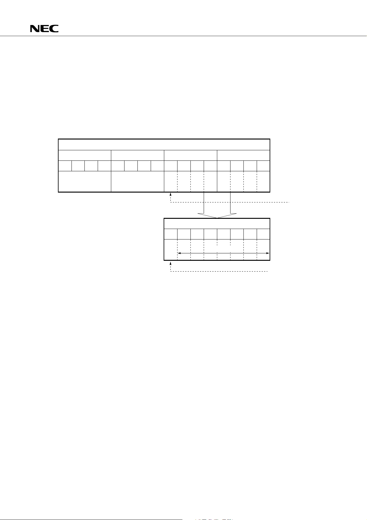
µ
PD17062
10.4.2 Precautions When Transferring Data With Peripheral Registers
Data is transferred between the data buffer and peripheral registers in 8-bit or 16-bit units.
A PUT or GET instruction is executed for one instruction cycle (2 µs) even if the data is 16 bits long.
When 8-bit data transfer is performed but the peripheral register execution data is seven bits, for example,
long one extra bit is added.
At data write, the status of this extra data is “Don’t care” as shown in Example 1. At data read, the status
of this extra data is “Unpredictable” as shown in Example 2.
Example 1. PUT instruction (When the valid peripheral register bits are seven bits from bit
Data buffer
DBF3 DBF2 DBF1 DBF0
15 b14 b13 b12 b11 b10 b9 b8 b7 b6 b5 b4 b3 b2 b1 b0
b
Don't care Don't care
8
Peripheral register
7 b6 b5 b4 b3 b2 b1 b0
b
Valid bits
PUT
0 or unpredictable
0 to bit6.)
Don't care
(Can be any value)
When 8-bit data is written to a peripheral register, the status of the eight high-order bits of the data buffer
(contents of DBF3 and DBF2) is “Don’t care”.
Of the 8-bit data in the data buffer, the status of each bit that does not correspond to a valid bit in the
peripheral register is “Don’t care”.
95

Example 2. GET instruction
Data buffer
DBF3 DBF2 DBF1 DBF0
15 b14 b13 b12 b11 b10 b9 b8 b7 b6 b5 b4 b3 b2 b1 b0
b
Don't careDon't care
8
Peripheral register
7 b6 b5 b4 b3 b2 b1 b0
b
Valid bits
GET
0 or unpredictable
The value of the
peripheral register
is read without alteration.
µ
PD17062
0 or unpredictable
When the 8-bit data of a peripheral register is read, the value of the eight high-order bits (DBF3 and DBF2)
of the data register does not change.
Of the 8-bit data of the data register, each bit that is not a valid peripheral register bit becomes 0 or
unpredictable. Whether the bit becomes 0 or unpredictable is decided in advance for each peripheral register.
10.4.3 State at Peripheral Register Reset
The valid bits of each peripheral register are reset as follows:
Reset Valid bit state
Power-on Unpredictable
Clock-stop Previous state held
CE Previous state held
96

10.5 Data Buffer and Peripheral Registers
Sections 10.5.1 to 10.5.7 describe the data buffer and the peripheral registers.
10.5.1 IDC Start Position Setting Register
Fig. 10-4 shows the functions of the IDC start position setting register.
The IDC start position setting register sets the IDC display start position.
Fig. 10-4 IDC Start Position Register Functions
Name Data buffer
Symbol
Address
Bit
DBF3
0CH
b
15b14b13b12b11b10b9b8b7b6b5b4b3b2b1b0
DBF2
0DH
DBF1
0EH
DBF0
0FH
µ
PD17062
Data Don't care Don't care
Name
IDC start position
setting register
Transfer data
Peripheral register
b7b6b5b4b3b2b1b
Valid data
D7 D6 D5 D4 D3 D2 D1 D0
GET
PUT
0
Symbol
IDCORG 01H
IDC display position setting
D7 to D4: Horizontal start position
D3 to D0: Vertical start position
Peripheral
address
Peripheral hardware
Image display
controller
97

µ
10.5.2 A/D Converter Data Register
Fig. 10-5 shows the functions of the A/D converter data register.
The A/D converter data register sets the A/D converter comparison voltage.
Because the A/D converter is a 4-bit converter, the four low-order bits of the A/D converter data register
are valid.
Fig. 10-5 A/D Converter Data Register Functions
Name Data buffer
Symbol
Address
Bit
DBF3
0CH
b
15b14b13b12b11b10b9b8b7b6b5b4b3b2b1b0
DBF2
0DH
DBF1
0EH
DBF0
0FH
PD17062
Data Don't care Don't care
Name
A/D converter
data register
Transfer data
8
Peripheral register
b7b6b5b4b3b2b1b
0000
Valid data
0
1
x
15
GET
PUT
x - 0.5
15
Peripheral
address
Symbol
0
ADCR 02H
A/D converter comparison voltage V
V
REF
= 0 V
V
REF
=V
Fixed at 0
Peripheral hardware
×
DD
(V)
A/D converter
REF
setting
98

µ
PD17062
10.5.3 Presettable Shift Register
Fig. 10.6 shows the functions of the presettable shift register.
The presettable shift register writes the serial interface serial out data and reads the serial interface serial
in data.
Fig. 10-6 Relationship between Presettable Shift Register and Data Buffer
Name Data buffer
Symbol
Address
Bit
DBF3
0CH
b15 b14 b13 b12 b11 b10 b9 b8 b7 b6 b5 b4 b3 b2 b1 b0
DBF2
0DH
DBF1
0EH
DBF0
0FH
Data Don't care Don't care
Name
Presettable
shift register
Transfer data
8
Peripheral register
b7 b6 b5 b4 b3 b2 b1 b0
Valid data
D7 D6 D5 D4 D3 D2 D1 D0
GET
PUT
Symbol
SIO0SFR 03H
Serial out data write and serial in data read
Serial out data
×D7 ×D6 ×D5 ×D4 ×D3 ×D2 ×D1 ×D0
Clock
12345678
MSB LSB
Peripheral
address
Data output timing
Peripheral hardware
Serial interface
Serial in data
×D7 ×D6 ×D5 ×D4 ×D3 ×D2 ×D1 ×D0
Clock
12345678
MSB LSB
Data input timing
Serial interface serial data is output while being shifted sequentially the data from the MSB (bit b
presettable shift register.
During serial data input, data is shifted sequentially from the LSB (bit b0).
7) of the
99

10.5.4 HSYNC Counter Data Register
Fig. 10.7 shows how the HSYNC counter data register functions .
The HSYNC counter data register reads the horizontal synchronizing signal count.
When the HSYNC counter data register reaches 3FH, it returns to 00H at the next input.
Fig. 10-7 HSYNC Data Register Functions
Name Data buffer
Symbol
Address
Bit
DBF3
0CH
15b14b13b12b11b10b9b8b7b6b5b4b3b2b1b0
b
DBF2
0DH
DBF1
0EH
DBF0
0FH
µ
PD17062
Data Don't care Don't care
Name
HSYNC counter
data register
Transfer data
8
Peripheral register
b7b6b5b4b3b2b1b
00
Valid data
GET
Symbol
0
HSC 04H
Horizontal synchronizing signal count
Peripheral
address
Peripheral hardware
synchronizing signal
Horizontal
counter
100
 Loading...