

Page 1

NAD
C 542
COMPACT
DISC PLAYER
C 542
COMPACT
DISC PLAYER
SERVICE MANUAL
Page 2

- 2 -
SAFETY INFORMATION
CAUTION
CAUTION
- INVISIBLE LASER RADIATION WHEN OPEN AND
INTERLOCKS DEFEATED. AVOID EXPOSURE TO BEAM.
ADVARSEL
- USYNLIG LASERSTRÅLING NÅR DEKSEL ÅPNES OG
SIKKERHEDSLÅS BRYTES. UNNGÅ EKSPONERING FOR STRÅLEN.
ADVARSEL
- USYNLIG LASERSTRÅLING VED ÅBNING, NÅR
SIKKERHEDSAFBRYDERE ER UDE AF FUNKTION. UNDGÅ
UDSÆTTELSE FOR STRÅLING.
VARING
- OSYNLING LASERSTRÅLNING NÄR DENNA DEL ÄR
ÖPPNAD OCH SPÄRRAR ÄR URKOPPLADE. STRÅLEN ÄR FARLIG.
VARO!
- AVATTAESSAJA SUOJALUKITUS OHITETTAESSA OLET
ALTTIINANÄKTMÄTÖNTÄ LASERSÄTEILYLLE. ÄLÄ KAISO
SÄTEESEEN.
VORSICT!
- UNSICHTBARE LASERSTRAHLUNG TRITT AUS, WENN
DECKEL GEÖFFNET UND WENN SICHERHEITSVERRIEGELUNG
ÜBERBRÜCKT IST. NICHTDEM STRAHL AUSSETZEN.
THIS DEVICE COMPLIES WITH PART 15 OF THE FCC RULES.
OPERATION IS SUBJECT TO THE FOLLOWING TWO CONDITIONS:(1) THIS DEVICE MAY NOT CAUSE HARMFUL INTERFERENCE, AND
(2) THIS DEVICE MUST ACCEPT ANY INTERFERENCE RECEIVED,
INCLUDING INTERFERENCE THAT MAY CAUSE UNDESIRED
OPERATION.
CATUION
ADVARSEL
KBVNCLKNBCVLKNLKNVLKNCVNCLVK JK
ADVARSEL
HFKLJHJLDKLJLKDJLKFHJHSGMMKJHGSJK
HGKJDHSGKJHGSJK
HGKJDHSGKJHGS
VARING
KLHKFG;LKNG;LKJGF;LKJGF;LKJFL;SJK
HG
HGKLFH;L;HJMNMD
KJDHSGKJHGKLG
VARO!
HGKJD
KBVN
CLKNB
HSGKJHJBJKBKJBJKGS
CVLKNLKN
VORSICT!
JHFKLJHJLDKLJLKDJLKFHJHSGKJHGSJK
HGKLFH;L;H
DJH
VLKNC
VNCLVK JK
HBH
HJD
CLASS 1
LASER PRODUCT
The lightning flash with arrowhead, within an equilateral tri-
angle is intended to alert the user of the presence of
uninsulated "dangerous voltage" within the product’s
enclosure; that may be of sufficient magnitude to consti-
tute a risk of electric shock to persons.
The exclamation point within an equilateral triangle is intend-
ed to alert the user of the presence of important operating
and maintenance (servicing) instructions in the literature
accompanying the appliance.
Page 3

- 3 -
SERVICE SAFETY PRECAUTIONS
1. Replacing the fuses
CAUTION: FOR CONTINUED PROTECTION AGAINST THE RISK OF FIRE REPLACE ONLY WITH SAME TYPE
OF FUSE.
Reference No Part Number Description
M507 *AH 5120-0052-0 FUSE T1.6A 250V 5x20MM
M507 *C 5120-0050-0 FUSE T1.6A 250V 5x20MM
M512, M513 *AH 5120-0020-0 FU T1A 250V UL/CSA 5x20MM
M512, M513 *C 5120-0018-0 FU T1A 250V SEMKO/VDE
M514 *AH 5120-0026-0 FU T315MA L 250V UL/CSA
M514 *C 5120-0027-0 FU T315MA L 250V
NOTE:
<*AH > : USA, CANADIAN MODEL ONLY.
<*C > : EUROPEAN MODEL ONLY.
2. Safety check out
(Only U.S.A. model)
Before returning the product to the customer, make leakage current or resistance measurements to determine that
exposed parts are acceptably insulated from the supply circuit.
Parts marked with the symbol are critical with regard to the risk of fire and electric shock.
Replace only with parts recommended by the manufacturer.
CONTENTS
DESCRIPTION PAGE
SPECIFICATIONS . . . . . . . . . . . . . . . . . . . . . . . . . . . . . . . . . . . . . . . . . . . . . . . . . . . . . . . . . .4
REAR PANEL / FRONT PANEL . . . . . . . . . . . . . . . . . . . . . . . . . . . . . . . . . . . . . . . . . . . . . . . . .5
DISASSEMBLY INSTRUCTIONS . . . . . . . . . . . . . . . . . . . . . . . . . . . . . . . . . . . . . . . . . . . . . . .6
BLOCK DIAGRAM . . . . . . . . . . . . . . . . . . . . . . . . . . . . . . . . . . . . . . . . . . . . . . . . . . . . . . . . . .7
WIRING DIAGRAM . . . . . . . . . . . . . . . . . . . . . . . . . . . . . . . . . . . . . . . . . . . . . . . . . . . . . . . . . .8
RF PATTERN TESTING . . . . . . . . . . . . . . . . . . . . . . . . . . . . . . . . . . . . . . . . . . . . . . . . . . . . . .9
IMPORTANT NOTES . . . . . . . . . . . . . . . . . . . . . . . . . . . . . . . . . . . . . . . . . . . . . . . . . . . . .10-11
PCB LAYOUT . . . . . . . . . . . . . . . . . . . . . . . . . . . . . . . . . . . . . . . . . . . . . . . . . . . . . . . . . .12-13
SCHEMATIC DIAGRAM . . . . . . . . . . . . . . . . . . . . . . . . . . . . . . . . . . . . . . . . . . . . . . . . . . .14-18
IC BLOCK DIAGRAM . . . . . . . . . . . . . . . . . . . . . . . . . . . . . . . . . . . . . . . . . . . . . . . . . . . . .19-22
TROUBLESHOOTING GUIDE . . . . . . . . . . . . . . . . . . . . . . . . . . . . . . . . . . . . . . . . . . . . . . . .23
ELECTRICAL PARTS LIST . . . . . . . . . . . . . . . . . . . . . . . . . . . . . . . . . . . . . . . . . . . . . . . .24-29
MECHANISM EXPLODED VIEW . . . . . . . . . . . . . . . . . . . . . . . . . . . . . . . . . . . . . . . . . . . . . .30
MECHANISM EXPLODED VIEW PARTS LIST . . . . . . . . . . . . . . . . . . . . . . . . . . . . . . . . . . . .31
EXPLODED VIEW . . . . . . . . . . . . . . . . . . . . . . . . . . . . . . . . . . . . . . . . . . . . . . . . . . . . . . . . .32
EXPLODED VIEW PARTS LIST . . . . . . . . . . . . . . . . . . . . . . . . . . . . . . . . . . . . . . . . . . . . .33-34
PACKING DIAGRAM . . . . . . . . . . . . . . . . . . . . . . . . . . . . . . . . . . . . . . . . . . . . . . . . . . . . . . . .35
Page 4

- 4 -
SPECIFICATIONS
Disc Capacity . . . . . . . . . . . . . . . . . . . . . . . . . . . . . . . . . . . . One Disc, 120 or 80 mm
Decoding . . . . . . . . . . . . . . . . . . . . . . . . . . . . . . . . . . . . . . . BURR-BROWN Delta Sigma 24bit
Digital Filter . . . . . . . . . . . . . . . . . . . . . . . . . . . . . . . . . . . . . . 8 Times oversample
Analog Filter . . . . . . . . . . . . . . . . . . . . . . . . . . . . . . . . . . . . . 4 pole active
Frequency Response . . . . . . . . . . . . . . . . . . . . . . . . . . . . . . +/- 0.5 dB, 5Hz - 20kHz
De-Emphasis Error . . . . . . . . . . . . . . . . . . . . . . . . . . . . . . . . +/- 0.3 dB
THD (at 0 dB, 1kHz) . . . . . . . . . . . . . . . . . . . . . . . . . . . . . . . 0.002%
Intermodulation Distortion . . . . . . . . . . . . . . . . . . . . . . . . . . . < - 100 dB
(19 + 20 kHz)
Dynamic Range . . . . . . . . . . . . . . . . . . . . . . . . . . . . . . . . . . 96 dB
Linearity . . . . . . . . . . . . . . . . . . . . . . . . . . . . . . . . . . . . . . . . +/- 0.5 dB, 0 dB to -80 dB
Signal / Noise Ratio (A-Weight) . . . . . . . . . . . . . . . . . . . . . . . ≥100 dB, De-Emphasis on
≥100 dB, De-Emphasis off
Channel Separation 1kHz . . . . . . . . . . . . . . . . . . . . . . . . . . >90 dB
10 kHz . . . . . . . . . . . . . . . . . . . . . . . . >80 dB
Wow and Flutter . . . . . . . . . . . . . . . . . . . . . . . . . . . . . . . . . . Unmeasurable (Quartz Crystal Accuracy)
Output Impedance . . . . . . . . . . . . . . . . . . . . . . . . . . . . . . . . 200 Ω
Output Level at 0 dB . . . . . . . . . . . . . . . . . . . . . . . . . . . . . . . 2.2 V rms
Digital Error Correction . . . . . . . . . . . . . . . . . . . . . . . . . . . . . IRC with double error correction in C1 and C2
Digital Code Output . . . . . . . . . . . . . . . . . . . . . . . . . . . . . . . . Sony / Philips Serial data format
Power Consumption . . . . . . . . . . . . . . . . . . . . . . . . . . . . . . . 12W
CONTROLS
Play / Pause, Stop, Random, Skip (< >), Scan (< >), Open, Time, Repeat.
PHYSICAL SPECIFICATIONS
Dimensions 435 x 80 x 285 mm
(Width x Height x Depth)
Net weight 4 kg (8.8 lbs)
Shipping weight 5.1 kg (11.22 lbs)
Page 5

- 5 -
DIGITAL
OPTICAL OUT
DIGITAL
OUT
TRIGGER SWITCH
OFF
AUTO
1. LINE OUT
2. DIGITAL OPTICAL & COAXIAL OUTPUT
3 NAD LINK IN / OUT
4. IR INPUT
5. TRIGGER IN
6. TRIGGER SWITCH
7. AC LINE CORD
1. POWER ON / OFF
2. DISC DRAWER
3. DISPLAY
4. OPEN
5. PLAY / PAUSE
6. TIME
7. STOP
8. REPEAT
9. RANDOM
10. SCAN Back ( ) / Forward ( )
11. SKIP Back ( ) / Forward ( )
12. STANDBY LED
REAR PANEL / FRONT PANEL
REAR PANEL
FRONT PANEL
DIGITAL
DIGITAL
OPTICAL OUT
OUT
' 2003 NAD C 542
NAD LINK
OUT
IN
IR IN
4
TRIGGER SWITCH
OFF
IN
5
AUTO
6
7
1151279
NA
D
' 2003 NAD C 542
Compact Disc Player
1
C 542
2
PLAY PAUSE
STOP
RANDOM
SEC
MIN
6 7 8
9
10
3
OPEN
REPEAT
TIME
468
SKIP
SCAN
10
Page 6

- 6 -
DISASSEMBLY INSTRUCTIONS
1. Remove machine screws M 4.0 x 6.0 ( 1 to 4 ) from the side panels.
Remove tapping screw 3.0 x 8.5 ( 5 )from the back panel.
Refer to Figure No.1.
Figure No.1
2. Pull both sides of the TOP COVER slightly outwards 6 and tilt approx. 35˚ and then remove
in the direction as indicated by the arrow 7 . Refer to Figure No.2.
Figure No.2.
5
4
3
1
2
7
6
6
Page 7
- 7 -
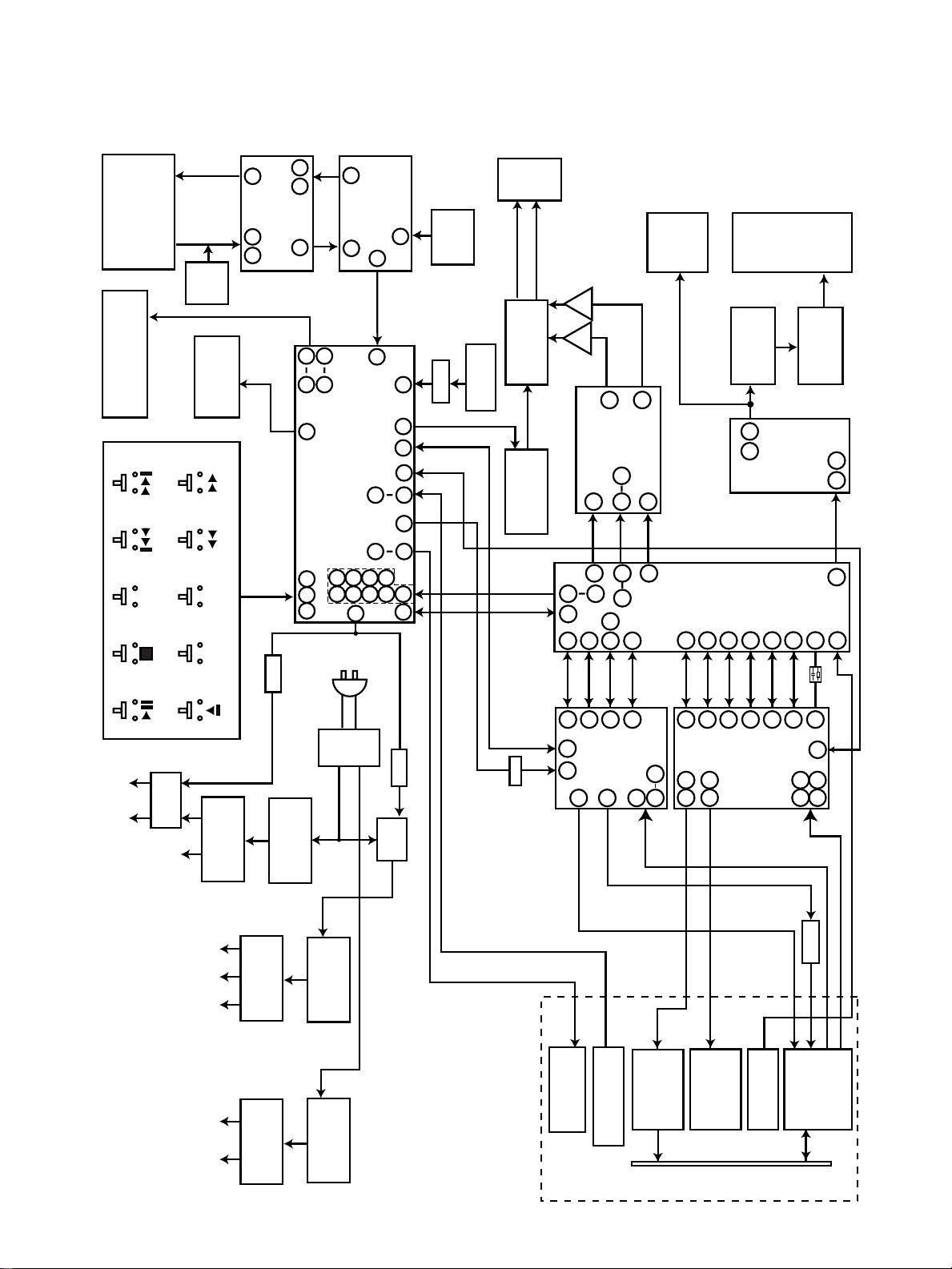
BLOCK DIAGRAM
NAD LINK
M319
RCA JACK
NAD LINK
M501
VFL DISPLAY
KEYBOARD
RANDOM
OUT
IN
M108M107
M105
M110 M109
M313
IR_IN
M314
TRIGGER
REPEAT
TIME
SWITCH
M102
M101
M106 M104 M103
1312
11
U403
109
8
74HC00 NAND GATE
41 56
1 79 80 24
Q312
15
U402
MICRO-
NAD LINK
CONTROLLER
9
11
23
35 40
63
U301 M38B59EF
SYSTEM CONTROL CPU
& VFL DISPLAY DRIVER
65
18 67
19 69
59 70
60 80
32
AC POWER I / P
O/P
M313
RCA
CD AUDIO
8
M113
SENSOR
REMOTE
M315
Q307
TRIGGER IN
68 72 25
64
66 58 67
6222
JACK
L
R
Q301-Q304
MUTE
Q401- Q403
MUTE CIRCUIT
U305
U306
L
27
64
1
20
515940 41
FE
RFAC
151618
9
16
U302
SETE
R
13
DAC
PCM1732
1 3
4
6361
66
U201
43
RFDC
28
M316
DIGITAL
OPT JACK
DSP
LXD3017Q
292833
SRDR
426 27
OUTPUT
SFDR
FRDR
5
FFDR
9
M318
M303
EMC FILTER
3 6
U403
32
313026
TRDR
10
201924
DIGITAL
OUTPUT
RCA JACK
L301
74HC00
NAND GATE
TFDR
SPDR
DIGITAL COIL
2 4
60
27
12 13
15
16 17
Q101
PICK
UP
POWER
K502
F1 F2
RELAY
-22V
D510-D511
ZENER DIODES
-12V
U502-3,U506
U501,U507
+8V +5V +12V 5V
RECTIFIER
D506-D508
POWER
ANALOGUE
POWER
DIGITAL
M500
TRANSFORMER
DIODES
DIODES
RECTIFIER
D501-D504
DIODES
RECTIFIER
D514-D517
K501
RELAY
Q310
U101
25 12
CX2581
Q103
MOTOR
LOADING
RF AMP
1
27
DISW
DISCO
LIMIT SWITCH
LOADING MOTOR
2
SPINDLE
CD MECHANISM UNIT
11
6
MOTOR
1 2
SLED
MOTOR
U202
BA6392
PU-IN
LIMIT SWITCH
DISC
Page 8

- 8 -
WIRING DIAGRAM
M120A
KEY BOARD
MAIN BOARD
M502
TRANSFORMER
RED
BROWN
M102
(16PIN)
M105A
(6PIN)
BLACK
M101
(5PIN)
CD MECHANISM
M301A
M505A
M506A
LED BOARD
DISPLAY BOARD
NEUTRAL
LIVE
LIVE BOARD
Page 9
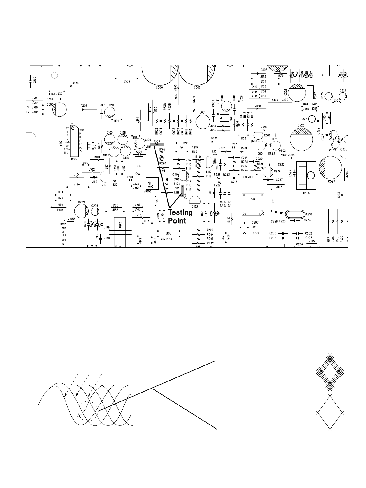
- 9 -
RF PATTERN TESTING
NAD - C 542 PCB TESTING POINTS DIAGRAM
TESTING PROCEDURE
(1) Load the test disc (Sony Test CD YEDS-7) and set the unit into PLAY mode.
(2) Connect the scope to R227 (Pin 15 of U101) and DGND (J144).
Scope setting: Coupling : AC.
Vertical sensitivity : 0.2 V/ div.
Horizontal time base : 0.5 µS/div.
(3) Observe the waveform is 2.0V p-p +/-5% and the eye pattern is at its best shape (see FIG. 1).
FIG. 1 (a) FIG. 1 (b) Poor eye pattern
FIG. 1 (C) Good eye pattern
3T 4T 5T — 11T
Page 10

- 10 -
IMPORTANT NOTES
INSTRUCTION FOR HANDLING OPTICAL SYSTEM BLOCK PICK-UP
Electrostatic breakdown of the laser diode in the optical system block may occur due to a potential difference caused
by electrostatic charge accumulated on clothing, human body, etc. A ground must be provided as follows to prevent
any electrostatic charge during unpacking or repair work.
1. Ground for Human Body
Be sure to wear a ground band (1M ohm) that is properly to remove any static electricity that may be charged on the
body.
2. Ground for Work Bench
Be sure to place a conductive sheet (1M ohm) or copper plate with proper grounding on the work bench or other sur-
face on which the pick-up is to be placed.
3. Because the static electricity charge on the clothing does not discharge through the body grounding band, do not
let clothing to get in contact with the pick-up unit.
PRECAUTIONS FOR CHECKING BEAM EMISSION
The laser beam of this unit is focused on the reflecting surface of the objective lens in the optical system block.
Therefore, keep your eyes at least 12 inches (30 cm) away from the objective lens when the laser diode is ON.
(Operation Check Method for Laser Diode and Focus Search Function.)
When the POWER switch is turned ON after the chucking plate is removed, observe the objective lens and confirm
that the following operations are performed properly.
(The optical system should be at the lead-in area position when it is checked at this time.)
(1) The laser should be at the innermost position after the chucking plate is removed.
(2) The diffused light of the laser beam can be seen when the POWER switch is turned ON.
(3) Vertical (up and down) movement of the objective lens (2 or 3 times) will take place.
INCORRECT CORRECT
NOTE: Laser diodes are so susceptible to damage from
static electricity that even if a static discharge does not
ruin the diode, it can shorten its life or cause it to work
improperly.
1.Grounding band
1M ohm
1M ohm
2.Conductive Sheet
or Copper Plate
Page 11

- 11 -
PRECAUTIONS WHEN CHANGING LASER PICK-UP
When removing the pick-up assembly, short circuit the PCB tracks on the optical block as show in the drawing in
order to protect the pick-up before removal.
NOTE: Replacement pick-up assemblies are supplied with the PCB pattern already protected.
DO NOT REMOVE THE SHORT CIRCUITS UNTIL YOU HAVE FINISHED FITTING THE PICK-UP.
Caution:
Laser diodes are extremely susceptible to damage from static electricity. Even if a static discharge does not ruin the
diode, it can shorten its life or cause it to work improperly. When replacing the pick-up, use a conductive mat, a
grounded soldering iron, and so on, to protect the laser diode from static damage.
Ground Conductive
Wrist Band for Body
Ground Line
Less than
10 ohm
Conductive Gum Mat
Soldering
Iron with
Ground
wire
Protective soldering place
for laser diode
Page 12

- 12 -
PCB LAYOUT
DISPLAY BOARD
KEY BOARD
LIVE BOARD
LED BOARD
Page 13

- 13 -
MAIN BOARD
Page 14

- 14 -
L302
10uH
VCC
R3083KR309
3K
X301
4.00M
UNLD
LOAD
XRST
XLAT
CLOK
DATA
SCOR
SYSM
RW/ROM/LDOFF
RW/ROM/LDOFF
SCLK
SQCK
1/2X
CD/CDR
DISCO
DI/SW
R331 4K7
R332
1K
R333 4K7
R328
4K7
R327 4K7
R334 4K7
SQSO
SENS
C301
33p
C302
33p
C303
0.01u
1
2
3
Q311
8050
D303
IN4148
R312
10K
R311 100K
C308
10u/16V
VCC
C304
0.1u
C305
220uF/16V
C307
47uF/10V
D+5V VCC
DAT
1
GND
2
VCC
3M113
REMOTE
+D5V
R313
10
C420
10uF/16V
TP301
M101
B.SCAN
M106
OPEN/CLOSE
M102
F.SCAN
M107
PREV
M103
REPEAT
M105
RANDOM
M104
TIME
M109
STOP
M108
NEXT
M110
PLAY
R303
6K2
R302
6K2
R305
2K
R304
2K
R307
1K
R306
1K
R310
3K
R301
1K
VCC
TP303
SYSM
SQSO
SENS
SCOR
DATA
CLOK
XLAT
XRST
LOAD
UNLD
SCLK
SQCK
1/2X
CD/CDR
DISCO
DI/SW
MUTE
R317
1K
R314
OPEN
R315 1K
M314
TRIG SW
AUTO
OFF
R318
470
R336
10K
D304
STANDBY
RED
GREEN
R319
560
1
2
3
Q309
8050
1
2
3
Q310
8050
R1316 4K7
D307
IN4148
K501C
RELAY SW
+10V
TP302
75/5
1
P74/AN4
2
P73/AN3
3
P72/AN2
4
P71/AN1
5
P70/AN0
6
P61/CT02
7
P60/CT1
8
P47/1NT2
9
/RESET
10
P91/XOUT
11
P90/XIN
12
VSS
13
XIN
14
XOUT
15
VCC
16
P46/T3OUT
17
P45/T1OUT
18
P44/PWM1
19
P43/BUZ01
20
P42/INT3
21
P41/INT1
22
P40/INT0
23
P87PWM0/FLD39
24
P8625P8526P8427VEE28P8329P8230STANDBY
31
POWER32P37/FLD31
33
P3634P3535P3436P3337P3238P3139P30
40
P17/FLD23
41
P16
42
P15
43
P14
44
P13
45
P12
46
P11
47
P10
48
P07FLD15
49
P06
50
P05
51
P04
52
P03
53
P02
54
P01
55
P00
56
P27/FLD7
57
P26
58
P25
59
P24
60
P23
61
P22
62
P21/FLD1
63
P20
64
P57
65
P56
66
P55
67
P54
68
P53
69
P52
70
P51
71
P50
72
AVSS
73
VREF
74
P65
75
P64
76
P63
77
P62
78
P77/AN7
79
76/6
80
U301
MCU
-VP
VCC
F1/01
1
F1/02
2
NP
3
6G/03
4
5G/04
5
4G/05
6
3G/06
7
NC
8
2G/07
9
1G/08
10
NC
11
P1/09
12
P2/10
13
P3/11
14
P4/12
15
NC
16
NC
17
P5/13
18
P6/14
19
P7/15
20
P8/16
21
NC
22
NC
23
P9/17
24
P10/18
25
P11/19
26
P12/20
27
NC
28
P13/21
29
P14/22
30
P15/23
31
P16/24
32
NC
33
F2/25
34
F2/26
35
TP318
VFD
VFD3
VFD4
VFD5
VFD6
VFD7
VFD8
VFD9
VFD10
VFD11
VFD12
VFD13
VFD14
VFD15
VFD16
VFD17
VFD18
VFD19
VFD20
VFD21
VFD22
VFD23
VFD24
F1
F2
VFD3
VFD4
VFD5
VFD6
VFD7
VFD8
VFD9
VFD10
VFD11
VFD12
VFD13
VFD14
VFD15
VFD16
VFD17
VFD18
VFD19
VFD20
VFD21
VFD22
VFD23
VFD24
VCC
R329
4K7
R330
OPEN
R321
10K
NADLINK
REM_IN
1
2
3
Q312
8050
K502C
RELAY SW
D308
IN4148
C419
103
C310
100uF/6V3
D409
U301-P50
IN4148
1
2
3
Q402
2SD1012F
1
2
3
Q403
2SA1015
R412
4K7
R413
47K
R406
7K5
R415
7K5
1
2
3
Q401
2SA1015
R416
47K
R405 22K
C408
22u/16V
D411
IN4148
C407
2200u
16V
D403
3V3
MUTE
A+12V
R403 10K
R335
10K
VCC
1
2
3
Q307
8050
R338 10K
C403
OPEN
R322
15K
D305
IN5393
C306
0.1u
VCC
SENSOR
1
3
2
M315
TRIGGER_IN
M38B59EF
MCU
SCHEMATIC DIAGRAM
Page 15

SL+
1
SL-
2
RCIN1
3
SRDR
4
SFDR
5
VREFI
6
VREFO
7
GND
8
FRDR
9
FFDR
10
RCIN2
11
FCS+
12
FCS-
13
GND1
14
MUTE
15
TRK+
16
TRK-
17
RCIN3
18
TFDR
19
TRDR
20
VCC
21
VCC1
22
VBIN
23
SPDR
24
VBIN1
25
SP-
26
SP+
27
GND2
28
GND
29
GND
30
U202
BA6392
SQSO
1
SQCK
2
XRST
3
SYSM
4
DATA
5
XLAT
6
CLOK
7
SENS
8
SCLK
9
VDD
10
ATSK
11
SPOA
12
SPOB
13
XLON
14
WFCK
15
XUGF
16
XPCK
17
GFS
18
C2PO
19
SCOR
20
COUT
21
MIRR
22
DFCT
23
FOK24LOCK
25
MDP26SSTP
27
SFDR
28
SRDR
29
TFDR
30
TRDR
31
FFDR
32
FRDR
33
VSS34TEST
35
TES1
36
XTST
37VC38FE39SE40
TE
41
CE
42
RFDC
43
ADIO
44
AVSS0
45
IGEN
46
AVDD0
47
ASYO
48
ASYI
49
BIAS
50
RFAC
51
AVSS3
52
CLTV
53
FILO
54
FILI
55
PCO
56
AVDD3
57
VSS
58
VDD
59
DOUT
60
LRCK
61
PCMID
62
BCK
63
EMPH
64
XVDD
65
XTAI
66
XTAO
67
XVSS
68
AVDD1
69
AOUT1
70
AIN1
71
LOUT1
72
AVSS173AVSS2
74
LOUT2
75
AIN2
76
AOUT2
77
AVDD2
78
RMUT
79
LMUT
80
U201
CXD3017Q
R2014K7
R2021K
R2031K
R2041K
R2051K
R2061K
R2071K
R2091K
R2101K
R2111K
R212
100K
R213 10K
R214 8K2
R215
4R7
R217
1K
R21815K
R21915K
R220100K
R221
OPEN
R222
0
R223
33K
R224 10K
R225 100K
R226
1M
R227
100
R228
3K3
R229
3K3
R230
10K
C207
0.1u
C208
0.1u
C209
1500p
C210
0.1u
C211
27p
C212
27p
C214
470p
C215
470p
C213
0.1u
XLAT
DATA
SYSM
XRST
SQCK
SQSO
TP201
TP202
TP203
TP204
TP205
TP206
TP207
TP208
TP209
/SQSO
/SQCK
/XRST
/SYSM
/DATA
/XLAT
/CLOK
/SENS
/SCLK
/GFS
/SCOR
/SQSO
/SQCK
/XRST
/SYSM
/DATA
/XLAT
/CLOK
/SENS
/SCLK
/GFS
/SCOR
V3V6
C201
220p
C202
220p
C203
0.01u
C204
220p
C205
220p
C206
330p
CLOK
SENS
SCLK
SCOR
CLOK
SENS
SCLK
SCOR
TP210
TP211
TP212
V3V6
VC
SFDR
SFDR
SRDR
SRDR
TFDR
TFDR
TRDR
TRDR
FFDR
FFDR
FRDR
FRDR
SPDR
SPDR
VC
VC
+8V
C229
470U/16V
TP213
/XRST
TE
SE
FE
FE
SE
TE
C217
0.1u
C216
0.01u
C219
0.47u
V3V6
C218
100p
V3V6
C221
0.01u
RFDC
RFAC
C220
0.47u
C223
1500p
V3V6
C222
0.1u
TP214
AGND
TP216
X210
16.9344M
TP217
TP218
C225
30p
C224
30p
EMPH
BCK
PCMD
LRCK
XLAT
DATA
SYSM
XRST
SQCK
SQSO
RFDC
RFAC
12345
6
M105A
6PIN
FCS-
FCS+
TRK-
TRK+
C226
0.33u/50V
D201
1N4001
L201
27uH
VCC
C230
100uF/10V
FCS-
FCS+
TRK-
TRK+
EMPH
BCK
PCMD
LRCK
C227
0.1u
C228
0.1u
CN202
DEBUG
R231
OPEN
CLKO
CLKOCLKO
DIG_OUT
XRSTA
DSP
R209
1K
- 15 -
DISPLAY
NOTE: 1. RESISTORS, ARE CARBON FILM 5% 1/8W
UNLESS OTHERWISE SPECIFIED.
2. CERAMIC CAPACITORS, ARE 50V 10%.
UNLESS OTHERWISE SPECIFIED.
Page 16

- 16 -
VC
1
VDD
2E3D4A5B6C7F8
GND
9
LD10VR
11
PD
12
FCS+
13
TRK+
14
TRK-15FCS-
16
M102
16PIN
LD1PD2EQ_IN3AC_SUM4GND5A6B7C8D9E10F11SW12DVCC13DVC14RFAC
15
FE
16
FEI17TE
18
TE_BAL
19CE20
CEI
21
VCC22RFG
23
BST
24
VFC25RFC
26
VC
27
RFDCO
28
RFDCI
29
DC_OFST
30
U101
CXA2581
1
2
3
Q101
8550
R101
10
R103 20K
R104 20K
R105
3K
R106
150K
R107
100K
R108
68K
R109 15K
R110 3K
R111 4K7
R112 5K1
R113
5K1
R114
5K1
R115 1K8
R116 12K
R117 12K
R118
10K
R119 15K
C101
0.1u
C102
0.1u
C105
100u/10V
C106
100u/10V
C107
100u/10V
C108
100u/10V
C109
100u/10V
VDD1
VC
VDD1
C110
100u/10V
VDD1
TP101
FE
TE
SE
SE
TE
FE
RFAC
RW/ROM/LDOFF
TP105
TP106
TP107
RFDC
FCS-
TRK-
TRK+
FCS+
FCS-
FCS+
TRK+
TRK-
L101
10uH
V3V6
RFDC
RFAC
RW/ROM/LDOFF
TP108
TP109
TP103
1
2
3
Q103
8050
1/2X
1/2X
TP104
12345
M101
5PIN
1
2
3
Q104
8550
1
2
3
Q105
8550
1
2
3
Q106
8050
1
2
3
Q107
8050
R121
1K
R122
1K
R123
1K
R124
1K
VCC
LOAD
UNLD
TRAY-
TRAY+
DI/SW
DISCO
DISCO
DI/SW
LOAD
UNLD
DI/SW
DISCO
R125
4R7
L102
10uH
C103
0.1u
Q106B
2.2u/50V
RF AMP
NOTE: 1. RESISTORS, ARE CARBON FILM 5% 1/8W UNLESS
OTHERWISE SPECIFIED.
2. CERAMIC CAPACITORS, ARE 50V 10%. UNLESS
OTHERWISE SPECIFIED.
Page 17

- 17 -
DAC
C378
M317A
A-12V
224K
R380
R376
R362
1
75R
75R
R396 4K7
C353 100p
4K7
A+5V
L
Q304
U306A
R397
C322
2
2SD655F
Q302
2SD655F
1
OPA2134PA
2
3
C363
4700p
R368
2K2
4K7
R364
1K5
7
R360 15.2K
6
AGND
C376
1415
U302
PCM1732U
104K
(A)
10u/25V
C323
R382
R372
2K2
5
R356
100u/16V
13
AGND1VCC1
161718
R414
4K7
R378
4K7
R374
100K
C367
680p
C357
2700p
U306B
OPA2134PA
4K7
R361
10K
C320
10u/16V
12
EXTR
VOUTR
VOUTL
EXTL
(A)
A-12V
4K7
(A)
11
MUTE
C370 103K
D+5V
AGND
10
VCC2R
AGND2R
AGND2L
VCC2L
19
C321
10u/16V
R
M317B
3
Q303
2SD655F
75R
R379
R375
75R
4K7
R395
A-12V
R394
4K7
C352
100p
R358
4K7
C375
100u/16V
C324
10u/16V
8
9
VDD
HDCD
GAIN
ZERO
202122
AGND
2
C536
103K
Q301
2SD655F
7
6
5
C362
4700p
R367
2K2
R363
1K5
1
R359 15.2K
2
3
R355
AGND
(A)
AGND
(A)
M302A
DGND
16.9344MHz
5
6
7
XTO
DGND
RST
CS/IWO
2324252627
M316
D+5V
C361
104K
R381
R377
R373
U305B
OPA2134PA
C366
R371
2K2
C356
2700p
U305A
OPA2134PA
4K7
R357
C377
224K
4
XTI
MODE
4K7
4K7
100K
680p
10K
3
CLKO
MUTE
DGND
DIGITAL OUT
1
R384
75R
4
3
1
2
C385
2200p
R383
150R
3
Vout
GND
Vin
1
C383
22u/10V
3
U403A
74HC00
2
C450
DIG_OUT
LED1
2
C387
2
OTP_DIG
104K
CHASIS
LED
R622
100R
CHASIS
C384
U403B
4
R337
4K7
1000p
6
74HC00
OTP_DIG
M318
OTP_DIG
M303
DST310
1
5
D+5V
C328
20p
L301
DGND
C329
20p
2
DIN
LRCIN
BCKIN
21
MD/FSS
MC/DEM
ML/I S
28
R320
470R
EMPH
DGND
LRCK
M319
CHASIS
103K
C386
104K
J528
D415
D414
12
DGND
U402
NADLINE_001
L401
LED2
LED
Q308
SS8050
PCMD
OUT
NAD LINE
1
R408
100R
1N4148
1N4148
11
74HC00
13
17
18
P23
P24
1
2
10uH
D+5V
CLKO
BCK
NAD LINE
M319
2
R409
U403D
R407
16
P22
P25
3
C413
C412
A+12V
IN
1
100R
R302
4K7
P21
P26
104K
104K
4K7
9
U403C
15
P20
P27
4
C372
470u/16V
D302
IN4148
D301
IN4148
C325
10u/16V
C334
10u/16V
100R
R301
2
C451
D412
1N4148
R410
100K
10
74HC00
8
14
GND
VCCX2X1
5
DGND
(A)
C374
D+5V
104K
R411
100R
D431
1N4148
13
P02
6
470u/16V
U306C
OPA2134PA
(A)
U305C
OPA2134PA
C326
104K
C409
C416
D413
12
7
8
8
104K
104K
1N4148
11
P01
8
C381
C380
IR_INPUT
CHASIS
DGND
NADLINK
TO CPU
P00
P31
P32 P33
D426 1N4148
910
M402A
12MHz
104K
4
104K
4
(A) (A)
C332
10u/25V
C327
104K
14
D+5V
A+5V
OTHERWISE SPECIFIED.
OTHERWISE SPECIFIED.
2. CERAMIC CAPACITORS, ARE 50V 10%. UNLESS
NOTE: 1. RESISTORS, ARE CARBON FILM 5% 1/8W UNLESS
IR_INPUT
132
M313
IR INPUT
IR_IN
27p
C415
27p
C414
C373
470u/16V
C371
470u/16V
A-12V
(A)
U403E
7
74HC00
C417
104K
C418
10u/6.3V
Page 18

- 18 -
P OW E R
NO TE : 1. R E S IS T O R S , AR E C AR BO N F IL M 5 % 1/8W UN L E S S
OT HE RW IS E S PE C IF IE D.
2. C E R AMIC C APAC ITOR S , AR E 50V 10% . U N L E S S
OT HE RW IS E S PE C IF IE D.
D+5V
C710
100u/6.3V
R518
470R
F2
F1
C514
R517
104K
470R
C513
104K
-22V
A+12V
A-12V
A+5V
D+8V
C541
104K
U501
7805 C511
K502B
RELAY
C508
U507
7808
C528
C529
470u/10V
3
Vout
Vin
1
470u/10V
C525
104K
3
Vout
Vin
1
104K
3300u/16V
GND
GND
2
C533
1000u/10V
2
DGND
D516
IN4001
DGND
D510
22V 1/2W
C521
3u3/50V
C510
22u/35V
C561
100u/16V
C560
100u/25V
D517
D508
1N4001
R523
R510
1K2
1N4001
D507
C540
DGND
47K
C522
1N4001
104K
3u3/50V
470R
R520
K502A
RELAY
D506
1N4001
D511
Q502
U502
5V6 1/2W
2SA950Y
3
Vout
LM317T
Vin
1
C545
104K
C506
1000u/25V
GND
C512
10u/25V
R501
240R
2
(A)
(A)
R503
C535
(A)
2K2
104K
C537
C539
10u/25V
10nF
AGND
(A)
C538
10u/25V
(A)
C544
R504
C534
10nF
2K2
104K
(A)
R502
C513
240R
2
U503
D505
10u/25V
LM337T
3V3 1.3W
3
Vout
GND
Vin
1
C546
C507
104K
1000u/25V
C527
1000u/10V
(A)
3
Vout
GND
2
Vin
U506
1
C525
470u/25V
C526
104K
AGND
7805
(A)
AGND
C543
104K
D514
M507
T1.6A 250V
1
9
3
M810
TLN120A150W3R0
1
IN4001
2
4
2
C501
104K
M514
T315mA 250V
3
1N5818
D504
1N5818
C504 104K
D503
D515
1N4001
C542
D512
104K
1N4001
DGND
RELAY
K501B
C502 104K
C503 104K
1N5818
D501
1N5818
C505 104K
D502
K501A RELAY
M512
T1A 250V
M513
T1A 250V
4
5
6
7
8
M502
10
J800
120V
J801
11
230V
C713
0.022u
TRANSFORMER TOROID
F1
F2
C800
4700p
POWER_SW
M802
FERRITE
RING
ONLY IN C VERSION
AC1
CORDEST
Page 19

- 19 -
MAIN BOARD
U101: CXA2581N
IC BLOCK DIAGRAM
MAIN BOARD
U202: BA6392FP
MAIN BOARD
U403: TC74HC00AP
1
BA
2
3
4
Out A
-In A
+In A
V-
8
7
6
5
V+
OUT B
_In B
+In B
+ — — +
MAIN BOARD
U305, U306: OPA2134
SW
PD
Vcc
GND
VC
DVC
22
5
27
14
1LD2
Vcc
VC
+
DVC
+
APC
VC
12
APC-OFF (Hi-Z)
RW/ROM
(H/L)
DVC
Vcc
VC
+
VOFST
D
RW/ROM
VC
DVC
-
+
F
11E10
gm
gm
VOFST
B
C
A
VC
+
+
-
DVC
-
DVcc
-
RW/ROM
VC
RW/ROM
+
VOFST
+
-
DVcc
RW/ROM
9D8C7B6
VOFST
RW/ROM
VC
DVC
A
AC
SUM
VC
VC
RW/ROM
+
-
+
DVcc
VCA
RW/ROM
EQ_ON/OFF
+
-
+
-
DVcc
EQ
AC
4
AC_SUM
3
EQ_IN
23
RFG
24
BST
26
RFC
25
VFC
1CH1OUTF 28 GND
2
3RCIN1 26 CH4OUTR
REV
4CH1RIN 25 VBIN
FWD
5CH1FIN 24 VSIN
6VREFIN 23 VBIN
7VREFOUT 22 VCC
8GND 21 VCC
FWD
9CH2FIN 20 CH3FIN
REV
10CH2RIN 19 CH3RIN
11RCIN2 18 RCIN3
12CH2OUTR 17 CH3OUTR
13CH2OUTF 16 CH3OUTF
14GND 15 MUTE
CH1OUTR
INTER
FACE
INTER
FACE
13
DVcc
F
R
-
+
R
F
DRIVE
MUTE
21
20
CEI
CE
LEVEL
SHIFT
190K
+
-
THERMAL
SHUTDOWN
CIRCUIT
R
F
25K
100K
INTER
FACE
25K
18
TE
27 CH4OUTF
FWD
REV
19
TE_BAL
16
FE
17
FEI
28
RFDCI
RFDCO
DC_OFST
30
29
1
A1
2
B1
3
Y1
4
A2
B2
5
Y2
6
GND
7
15
RFAC
14
13
12
11
10
VCC
B4
A4
Y4
B3
A3
9
Y3
8
Page 20

- 20 -
MAIN BOARD
U201: CXD3017Q
RFAC
ASYI
ASYO
BIAS
XPCK
FILO
FILI
PCO
CLTV
MDP
LOCK
SENS
DATA
XLAT
CLOK
SPOA
SPOB
XLON
SCOR
SQSO
SQCK
RFDC
CE
TE
SE
FE
VC
IGEN
XTSL
37
Clock
Generator
51
49
Asymmtery
48
50
17
54
55
56
53
26
25
12
13
14
20
43
42
41
40
39
38
46
Corrector
Digital
PLL
Digital
CLV
8
5
6
7
1
2
CPU
Interface
Signal Processor Block
Servo Block
OPAmp
Analog SW
XUGF
16
EFM
demodurator
Sub Code
Processor
Sequencer
A/D
Converter
GFS
18
Servo
Auto
EMPH
WFCK
15
64
Error
Corrector
16K
RAM
FOCUS SERVO
C2PO
19
D/A
Interface
SERVO
Interface
MIRR
DFCT
FOK
SERVO DSP
TRACKING
SERVO
SLED SERVO
LRCK
62
61
Digital
OUT
PCMD
BCK
63
SYSM
4
Serial-In
Interface
Over sampling
Digital Filter
3rd-Order
Noise Shaper
PWM PWM
-
+
-
+
PWM GENERATOR
FOCUS PWM
GENERATOR
TRACKING PWM
GENERATOR
SLED PWM
GENERATOR
Timing
Logic
DAC Block
-
+
-
+
36
35
3
79
80
66
67
70
71
72
77
76
75
60
9
21
27
11
22
23
24
32
33
30
31
28
29
TES1
TEST
XRST
RMUT
LMUT
XTAI
XTAO
AOUT1
AIN1
LOUT1
AOUT2
AIN2
LOUT2
DOUT
SCLK
COUT
SSTP
ATSK
MIRR
DFCT
FOK
FFDR
FRDR
TFDR
TRDR
SFDR
SRDR
44
ADIO
Page 21

- 21 -
Port P5(8)
8
Port P6(6)
6
Port P7(8)
8
Port P8(8)
RAM
8
Port P9(2)
2
Port P0(8)
A-D converter
(10-bit X 12 channel)
Serial I/O
Serial I/O1(Clock-synchronized)
(256 byte automatic transfer)
Serial I/O2
(Clock-synchronized or UART)
Timers
Timer X(16-bit)
Timer 1(8-bit)
Timer 2(8-bit)
Timer 3(8-bit)
Timer 4(8-bit)
Timer 5(8-bit)
Timer 6(8-bit)
System clock generation
X
IN-XOUT
(main-clock)
X
CIN-XCOUT
(sub-clock)
I/O ports
Build-in peripheral functions
8
Port P1(8)
8
Port P2(8)
8
Port P3(8)
8
Port P4(8)
1
7
ROM
Memory
CPU core
PWM1(8-bit)
PWM0(14-bit)
FLD display function
Buzzer output
Watchdog timer
Interrupt interval
determination function
40 control pins
(36 high-breakdown voltage ports)
65P57/SRDY2/SCLK22 40 P30/FLD24
66P56/SCLK21 39 P31/FLD25
67P55/TXD 38 P32/FLD26
68P54/RXD 37 P33/FLD27
69P53/SCLK12 36 P34/FLD28
70P52/SCLK11 35 P35/FLD29
71P51/SOUT1 34 P36/FLD30
72P50/SIN1 33 P37/FLD31
73AVSS 32 P80/FLD32
74VREF 31 P81/FLD33
75P6t/SSTB1/AN11 30 P82/FLD34
76P64/INT4/SBUSY1/AN10 29 P83/FLD35
77P63/AN9 28 VEE
78P62/SRDY1/AN8 27 P84/FLD36
79P77/AN7 26 P85/RTP0/FLD37
80P76/AN6 25 P86/RTP1/FLD38
1P75/AN5
64 P20/BUZ02/FLD0
2P74/AN4
63 P21/FLD1
3P73/AN3
62 P22/FLD2
4P72/AN2
61 P23/FLD3
5P71/AN1
60 P24/FLD4
6P70/AN0
59 P25/FLD5
7P61/CNTR0/CNTR2
58 P26/FLD6
8P60/CNTR1
57 P27/FLD7
9P47/INT2
56 P00/FLD8
10RESET
55 P01/FLD9
11P91/XCOUT
54 P02/FLD10
12P90/XCIN
53 P03/FLD11
13VSS
52 P04/FLD12
14XIN
51 P05/FLD13
15XOUT
50 P06/FLD14
16VCC
49 P07/FLD15
17P46/T3OUT
48 P10/FLD16
18P45/T1OUT
47 P11/FLD17
19P44/PWM1
46 P12/FLD18
20P43/BUZ01
45 P13/FLD19
21P42/INT3
44 P14/FLD20
22P41/INT1
43 P15/FLD21
23P40/INT0
42 P16/FLD22
24P87/PWM0/FLD39
41 P17/FLD23
MAIN BOARD
U301: M38B57MC
Page 22

INPUT
Port 3
Counter
Timers (2)
Interrupt
Control
Two Analog
Comparators
Port 2
I/O
(Bit Programmabel)
1
P24
P25
P26
P27
P28
XTAL 2
XTAL 1
P31
P32
P23
P22
P21
P20
GND
P02
P01
P00
P33
18
910
I/O
Vcc
ALU
OTP
Program
Counter
Machine
Timing & Inst.
Control
FLAG
Flegister
Pointer
General-Purpose
Register File
Port 0
GND
XTAL
- 22 -
OUT
IN
GND
MAIN BOARD
U501, U506, U507: 78XX
128
ML/I
2
SLRCIN
227
MC/DEMDIN
326
MD/F
SS
BCKIN
Serial
Input
I/F
Mode
Control
I/F
SCK
BPZ Control
Crystal/OSC
XTI XTO CLKO VCC1 AGND1 VDDDGND
Power Supply
Power-On Reset
HDCD
8X
Oversampling
Digital Filter with
Enhanced
Multi-level
Delta Signal
Modulator
DAC
Low-pass
Filter
V
OUT
L
V
CC
2L
AGND2L
V
CC
2R
AGND2R
EXTL
V
OUT
R
EXTR
ZERO
Low-pass
Filter
DAC
LRCIN
DIN
MUTE
RST
MODE
CS/IWO
MD/FSS
MC/DEM
ML/I
2
S
BCKIN
425
MUTECLKO
524
MODEXTI
623
CS/1WOXTO
7
PCM1732U
22
RSTDGND
821
20
ZEROV
DD
9
GAINHDCD
10 19
VCC2LVCC2R
11 18
AGND2LAGND2R
12 17
EXTLEXTR
13 16
V
OUT
LV
OUT
R
14 15
VCC1AGND1
HDCD
Hidden
Code
Recovery
HDCD
Amplitude
Decoding
MAIN BOARD
U302: PCM1732
MAIN BOARD
U402: NADLINK (MASKED)
Page 23

- 23 -
TROUBLESHOOTING GUIDE
SET POWER SWITCH TO ON.
IS POWER TURNED ON ?
YES
CAN TRAY BE OPENED ?
YES
CAN TRAY BE CLOSED ?
YES
DOES INITIAL READING OCCUR ?
YES
NO NO NO
NO
CHECK FUSES
M507, M512-M514 OPEN ?
YES
M507,M512-M514 DEFECTIVE CRYSTAL X301 DEFECTIVE.
IS THERE OPEN/ CLOSE KEY SIGNAL
INPUT ? U401 PIN 66, 65
YESNO
CHECK OPEN/ CLOSE SIGNAL AT U401
PIN 65 PIN 66
TRAY OPEN H L
TRAY CLOSE L H
YES
IS LOADING MOTOR DRIVE CIRCUIT
OPERATION NORMAL ?
YES
LOADING MOTOR AND LEAD WIRE DEFECTIVE
OR LOADING PART OF MECHANISM DEFECTIVE.
CHECK LASER LIGHT ? DOES LENS MOVE UP AND DOWN ?
YES YES YES
CHECK LASER CIRCUIT CORRECT ?
YES
CONNECTION OR PICKUP DEFECTIVE.
CHECK POWER SUPPLY
CIRCUIT NORMAL ?
YES
IS OSCILLATOR CIRCUIT
OSCILLATING ?
NONO
NO
NO
NO NO
M101 SWITCH, DEFECTIVE
OR PATTERN AND CONNECTOR OPEN.
MICROPROCESSOR IC U401 DEFECTIVE.
MOTOR DRIVE TRANSISTOR Q104,
Q105, Q106, Q107 DEFECTIVE.
RF SIGNAL OUTPUT ?
YES
FEED MOTOR OR WIRING DEFECTIVE.
NO
U101 DEFECTIVE.
POWER SUPPLY PATTERNS OPEN
OR U501-U507 DEFECTIVE.
NO
U101 DEFECTIVE.
NO
CHECK FOCUS SIGNAL OUTPUT ?
CHECK CONNECTION OR PICKUP.
CAN DISC BE PLAYED ? CHECK TRACKING SERVO CIRCUIT CORRECT ? SERVO IC U101 OR U202 DEFECTIVE.
YES
AUDIO OUTPUT IS CORRECT ? IS POWER SUPPLY NORMALLY ? CHECK POWER SUPPLY PATTERNS.
YES
OK
NO
YES
CHECK DISC OR MECHANISM AND CONNECTOR
NO
YES
CHECK CLOCK PULSE AT PIN4 OF U302
YES
CHECK OUTPUT PULSE AT PIN 61,62,63 OF U201
YES
CHECK OUTPUT SIGNAL AT PIN 13,16 OF U302
YES
CHECK OUTPUT SIGNAL AT PIN 1,7 OF U305, U306
YES
CHECK MUTE CIRCUIT Q301, Q302, Q303, Q304
YES
LINE OUT PLUG OR PATTERNS DEFECTIVE.
NO
NO
NO
NO
NO
NO
NO
M302 OR U302 DEFECTIVE.
IC U201 DEFECTIVE.
IC U302 DEFECTIVE.
IC U305 OR U306 DEFECTIVE.
MUTE CIRCUIT DEFECTIVE.
Page 24

- 24 -
DISP ASSY
PC BOARD
PCB-N0A70C-DISP PCB ASSY DISP N0A70C
WIRE
M505A 7009-9620-0 CONN WIRE ASSY 12P 100MM
M506A 7010-2224-0 CONN WIRE ASSY AWG28
PC BOARD
1725-711A-0000 PCB KEY N0A7XC C542
MISCELLANEOUS
0017 4134-8701-0 HOLDER, VFD CORNER
0024 4152-4841-1 BLACK CUSHION (EL/LCD)
LED1 3700-5810-R LED RED 5X5MM RT
M113 4816-043T-3 IR SENSOR PIC-26043TM2
M501 2460-1870-0 VFD 6-BT-271GK
KEY
ASSY
PC BOARD
PCB-N0A70C-KEY PCB ASSY KEY N0A70C
RESISTOR
R301,R306,R307 4701-102J-2 RCF 1/8W 1K 5% AT
R302,R303 4701-622J-2 RCF 1/8W 6.2K 5% AT
R304,R305 4701-202J-2 RCF 1/8W 2K 5% AT
SWITCH
M101-M110 5200-3538-0 SWITCH, TACT SKHHBY 7MM
WIRE
M120A 7012-6347-0 CONNECTOR WIRE ASSY
PC BOARD
1725-191B-0000 PCB KEY N0A70C
LED
ASSY
PC BOARD
PCB-N0A70C-LED PCB ASSY LED N0A70C
ELECTRICAL PARTS LIST
Reference No. Part No. Description
Page 25

- 25 -
LED
D304 3700-3517-RG LED RED/GREEN (L-469HGW)
WIRE
M301A 7703-1280-2004 CONN.ASSY 3P P2.5 L=280
PC BOARD
1725-201B-0100 PCB MAIN N0A70C C542
LIVE ASSY
PC BOARD
*AH PCB-N0A70C-LIVE PCB ASSY LIVE N0A70C
*CE PCB-N0A71C-LIVE PCB ASSY LIVE N0A71C
SWITCH
M802 5200-3151-0-01 POWER SWITCH
PC BOARD
1725-201B-0100 PCB MAIN N0A70C C542
MISCELLANEOUS
C800 8910-0049-0 CAP400V 4700P
M801,M806 4132-1071-0 TERMINAL PIN
M810 *CE 1806-2170-0 EMI FILTER TLN12UA
MAIN
ASSY
PC BOARD
PCB-N0A70C-MAIN PCB ASSY MAIN N0A70C
CAPACITOR
C102,C103,C207,C208,C210, 150F-104K-2-FC CC 50V 0.1UF 10% AT
C213,C217,C222,C227,C228,
C304,C322,C386,C409,C412,
C413,C416,C417,C450,C528
C105-C110,C230 157C-107M-5-IUE CE 10V 100µF 20% RL 5X11
C111 157F-225M-5-IUNK CE 50V 2.2µF 20% RL 5X11
C201,C204 150F-221K-2-FC CC 50V 220pF 10% AT 3.5x2
C203,C216,C221 150F-103K-2-FC CC 50V 0.01µF 10% AT 3.5x2
C206 150F-331K-2-FC CC 50V 330pF 10% AT 3.5x2
C209,C223 153F-152J-5-JM CM 50V 1500PF 5% RL 5.5x7
C211,C212,C414,C415 15CH-270J-5-GG CTC 0/60 27pF 5% RL 4x4
C214,C215 150F-471K-2-FC CC 50V 470pF 10% AT 3.5x2
Reference No. Part No. Description
Page 26

- 26 -
C218 150F-101K-2-FC CC 50V 100pF 10% AT 3.5x2
C219,C220 150F-474M-5-II CC 50V 0.47µF 20% RL 5X5
C226 157F-334M-5-GMK CE 50V 0.33µF 20% RL 4x7
C229 157D-477M-5-OVK CE 16V 470µF 20% RL 8x11.5
C303,C370 153F-103J-5-IM CM 50V 0.01µF 5% RL 5X7
C305 157D-227M-5-OMK CE 16V 220µF 20% RL 8x7
C306,C514,C515 150F-104K-5-II CC 50V 0.1µF 10% RL 5x5
C307 157C-476M-5-IMK CE 10V 47µF 20% RL 5X7
C308,C325,C334,C418,C420 157D-106M-5-GMK CE 16V 10µF 20% RL 4x7
C310,C710 157B-107M-5-KMK CE 6.3V 100µF 20% RL 6x7
C320,C321,C323,C324,C332 157D-106M-5-IUF3 CE 16V 10µF 20% RL 5X11
C328,C329 15CH-200J-5-GG CTC 0/60 20pF 5% RL 4x4
C352,C353 158F-101J-5-KW CP 50V 100pF 5% RL 6x12
C356,C357 153F-272J-5-JM CM 50V 2700PF 5% RL 5.5x7
C362,C363 153I-472K-9-NL CM 63V 0.0047µF 10% RB 7.5x6.5
C366,C367 158F-681J-5-KW CP 50V 680pF 5% RL 6x12
C371-C374,C527 157D-477M-5-X9F3 CE 16V 470µF 20% RL 12.5x20
C375,C376 157E-107M-5-S5C CE 25V 100µF 20% RL 10x16
C377,C378 153I-224J-9-NL CM 63V 0.22µF 5% RB 7.5x6.5
C383 157C-226M-5-IUK CE 10V 22µF 20% RL 5X11
C384 150F-102K-2-FC CC 50V 1000pF 10% AT 3.5x2
C385 150F-222K-2-GD CC 50V 0.0022µF 10% AT
C387,C419,C539,C544 153F-103K-5-IM CM 50V 0.01µF 10% RL 5x7
C407 157D-228M-5-X9E CE 16V 2200µF 20% RL 12.
C506,C507 157E-108M-5-5$F3 CE 25V 1000µF 20% RL 12.5x20
C508,C533 157C-108M-5-S5K CE 10V 1000µF 20% RL 16x31.5
C510 157F-107M-5-OVK CE 50V 100µF 20% RL 10x16
C511 157C-227M-5-OMK CE 10V 220µF 20% RL 8x7
C512,C513,C537,C538 157E-106M-5-IUF3 CE 25V 10µF 20% RL 5X11
C521 157F-226M-5-IUK CE 50V 22µF 20% RL 5X11
C522 157Q-476M-5-LUA CE 35V 47µF 20% RL 6.5X11
C525 157C-108M-5-X&F3 CE 10V 1000µF 20% RL 12.5x25
C529 157D-338M-5-5&K CE 16V 3300µF 20% RL 16x25
C560 157E-107M-5-KUK CE 25V 100µF 20% RL 6.3x11
C561 157D-107M-5-KUK CE 16V 100µF 20% RL 6.3x11
C713 153F-223K-5-LQ CM 50V 0.022µF 10% RL 6.5x9
COIL
L101,L102,L302 1801-100K-M COIL 10µH 10% BL7.0
L201 1801-270K-M COIL 27 µH,10%,AL,BL7
L301 1802-0450-0 DIGITAL COIL
WAFER/CONNECTOR
M102 2101-1382-0 CONNECTOR FLEXIBLE 16P
M120B 2102-051S-004 5P ST.WAFER
Reference No. Part No. Description
Page 27

- 27 -
M301B 2102-031S-004 3 PIN ST. WAFER
M502 2101-1811-0 8P PIN CONNECTOR P=3.96
M505B 2102-121S-004 12P ST.WAFER
M506B 2102-161S-004 16P ST WAFER P=2.5
JACK
M313,M315 2113-1743-0 MONO JACK HTJ-035-12E
M317 2113-1300-0 2P RCA JACK W/R AU
M318 2113-1170-0 1P RCA JACK YL AU
M319 2113-1121-0 2P RCA JACK Y/Y AU
CRYSTAL
M302 2300-1910-0 X'TAL 16.9344MHZ
SCREW
2954-2608-3000 SCREW BT 2.6X8 BLACK
2954-3008-0000 TAPPING 3X8MM B-TITE
IC
U101 3131-8030-0 IC CXA2581N ASP FOR CD S
U201 3131-8000-0 IC CXD3017Q DSP FOR CD
U202 3131-8040-0 IC BA6392FP 4-CHANNEL
U301 3131-8010-1 IC M38B57MC MICRO MASK
U302 3131-9380-0 IC PCM1732 HDCD DIA
U305,U306 3131-7620-0 IC OPA2134PA DIP OP AMP
U402 3130-9320-0 IC NADLINK (MASKED)
U403 3130-4160-0 IC TC74HC00AP DIGITAL
U501,U506 3130-2020-3 IC 7805 REG 5V 1.5A
U502 3130-5610-0 IC LM317T+ADJ REGULATOR
U503 3130-5620-0 IC LM337T-ADJ REGULATOR
U507 3130-2790-1 IC NJM7808FA +8V REG
RELAY
K501,K502 4500-0200-1 RELAY 2P2T BT-12S 12VDC
RESISTOR
4701-100J-2 RCF 1/8W 10R 5% AT
J178,R227,R3,R408,R409,R411 4711-101A-2 RMF 1/8W 100R 1% AT
R1,R111,R201,R316,R327,R328, 4711-472A-2 RMF 1/8W 4.7K 1% AT
R329,R331,R333,R334,R337,
R355,R356,R358,R362,R377,
R378,R381,R382,R394,R395,
R396,R397,R407,R412
R103,R104 4711-203A-2 RMF 1/8W 20K 1% AT
Reference No. Part No. Description
Page 28

- 28 -
R105,R110,R30-R310 4711-302A-2 RMF 1/8W 3K 1% AT
R106 4711-154A-2 RMF 1/8W 150K 1% AT
R107,R212,R220,R225,R311, 4711-104A-2 RMF 100K 1/8W 1% AT
R373,R374,R410,R414
R108 4711-683A-2 RMF 1/8W 68K 1% AT
R109,R119,R218,R219,R322 4711-153A-2 RMF 1/8W 15K 1% AT
R112,R113,R114 4711-512A-2 RMF 1/8W 5.1K 1% AT
R115 4711-182A-2 RMF 1/8W 1.8K 1% AT
R116,R117 4711-123A-2 RMF 1/8W 12K 1% AT
R118,R213,R224,R230,R312, 4711-103A-2 RMF 1/8W 10K 1% AT
R321,R335,R336,R338,R357,
R361,R403
R121-R124,R202-R207, 4711-102A-2 RMF 1/8W 1K 1% AT
R209-R211,R217,R315,R317,
R332,R402
R125,R215 4701-4R7J-C RCF 1/8W 4.7R 5% ATS
R214 4711-822A-2 RMF 1/8W 8.2K 1% AT
R223 4711-333A-2 RMF 1/8W 33K 1% AT
R226 4711-105A-2 RMF 1/8W 1M 1% AT
R228,R229 4711-332A-2 RMF 1/8W 3.3K 1% AT
R318,R320,R517,R518,R520 4711-471A-2 RMF 1/8W 470R 1% AT
R319 4711-561A-2 RMF 1/8W 560R 1% AT
R359,R360 4711-1522-2 RMF 1/8W 15.2K 1% AT
R363,R364 4711-152A-2 RMF 1/8W 1.5K 1% AT
R367,R368,R371,R372,R503,R504 4711-222A-2 RMF 1/8W 2.2K 1% AT
R375,R376,R379,R380,R384 4711-750A-C RMF 1/8W 75R 1% ATS
R383 4711-151A-C RMF 1/8W 150R 1% ATS
R405 4711-223A-2 RMF 1/8W 22K 1% AT
R406,R415 4711-752A-2 RMF 1/8W 7.5K 1% AT
R413,R416,R523 4711-473A-2 RMF 1/8W 47K 1% AT
R501,R502 4711-241A-2 RMF 1/8W 240R 1% AT
DIODE
4804-0010-2 DIODE 1N4001 AT
D301-D303,D307,D308,D404, 4804-1480-2 DIODE 1N4148 AT
D409,D411-D415,D426,D431
D305 4805-3930-2 DIODE 1N5393 200V 1.5A
D403 4837-3V36-2 DZ 1/2W +-5% 3.3V TEMIC
4837-5B61-2 DZ 1/2W 5.45-5.73 ROHM
D501-D504 4808-18R0-2 DIODE IN5818R-ND AT
D505 4840-1140-0 ZD 1.3W 3.3V 5% AT
D510 4837-22D1-2 DZ 1/2W 21.52~22.63V
Reference No. Part No. Description
Page 29

- 29 -
TRANSISTOR
Q101,Q104,Q105 4860-0060-5 TR SS8550 C/D SAMSUNG RL
Q103,Q106,Q107,Q307-Q312 4860-0050-5 TR SS8050 C/D SAMSUNG RL
Q301-Q304 4860-1780-5 TR 2SD655F HFE:600-1200
Q401,Q403 4860-0660-5 TR 2SA1015 (G.R.) RL
Q402 4851-012F-5 TR 2SD1012F/G HFE
Q404 485A-114E-5 TR DTA114ESA ROHM
Q405 485C-114E-5 TR DTC114ES
Q502 485A-950Y-5 TR 2SA950-Y HFE 100-200
SWITCH
M314 5200-3171-0-01 DPDT SLIDE
HEATSINK
U501-U503,U506,U507 5400-9130-0 HEAT SINK FOR 7805 2438-
WIRE
M101 7012-6536-0 CONN WIRE ASSY 5PIN P2.0
M102C 7012-6232-0 WIRE CON 16P P=1.0
M105A 7012-6538-0 CONN WIRE ASSY 6PIN P2.0
PC BOARD
1725-201B-0100 PCB MAIN N0A70C C542
MISCELLANEOUS
GND1 4132-1061-0 SOLDER TAG
M302 4152-9052-0 CRYSTAL CUSHION (BOTTOM)
M302 4152-9042-0 CRYSTAL CUSHION (TOP)
M303 2704-0060-0 EMC FILTER
M316 4811-F32T-3 LIGHT TX UNIT GP1F32T
M402 2703-0190-0 CR RESONATOR
M507,M512,M513,M514 4131-9131-0 FUSE HOLDER 6.5MM PITCH
U502,U503 2601-2608-0601 FIBRE WASHER M2.6 0.8T
2703-0150-1 CR4.00MHE,CSTLS4M00G55-B
Reference No. Part No. Description
NOTE: - The components identified by
mark are critical for risk of fire and electrical shock.
Replace only with part number specified.
- <*AH > : USA, Canadian model only.
- <*C > : European model only.
- Capacitors : CP-Polystyrene, CM-Mylar, CE-Electrolytic, CC-Ceramic, CTC-NPO.
- Resistors : RMF-Metal Film, RCF-Carbon Film, RWR-Wirewound Metal Oxide.
Page 30

- 30 -
MECHANISM EXPLODED VIEW
27
11
3
15
28
29
22
10
1
9
24
(x2)
21
(x4)
(x2)
(x4)
23
30
31
(x2)
8
26
26
5
12
17
16
6
25
(x2)
(x2)
14
32
20
13
25
19
18
(x2)
2
7
4
WSL-2130CCM
Page 31

- 31 -
1 4102-9000-0 Outside Main Chassis 1
2 4102-9001-0 Tray 1
3 4102-9002-0 Subchassis 1
4 4102-9003-0 Chucking Plate 1
5 4102-9004-0 Drive Gear 1
6 4102-9005-0 Control Cam 1
7 4102-9006-0 Chucking Pulley 1
8 4102-9007-0 Gear Cover 1
9 4102-9008-0 Tray Gear 1
10 4102-9009-0 Intermediate Gear 1
11 4102-9010-0 Loading Pulley 1
12 4102-9011-0 Motor Pulley 1
13 4102-9012-0 SW Pin 1
14 4102-9013-0 Chucking Yoke 1
15 4102-9014-0 Optical Pickup Unit 1
16 4102-9015-0 Loading PWB 1
17 4102-9016-0 Motor RF-500TB-14415 1
18 4102-9017-0 Leaf Switch 1
19 4102-9018-0 Connector pin (5P) 1
20 4102-9019-0 Magnet 1
21 4102-9020-0 Insulator 4
22 4102-9021-0 Coil Spring (Front) 2
23 4102-9022-0 Coil Spring (Rear) 2
24 4102-9023-0 Screw-Motor M2.6x2.5 2
25 4102-9024-0 Screw M2.6x7 2
26 4102-9025-0 Screw Washer Based M2.6x16 4
27 4102-9026-0 Rubber Belt 1
28 4102-9027-0 Center Ring 1
29 4102-9028-0 Turn Table 1
30 4102-9029-0 Gear (A) 1
31 4102-9030-0 Motor Gear 1
32 4102-9031-0 Damper 1
MECHANISM EXPLODED VIEW PARTS LIST
Item Part No. Description Qty
Page 32

- 32 -
EXPLODED VIEW
M500
Page 33

- 33 -
0001 *AH GREY/*CE GREY 1466-5103-0 FASCIA BLACK (C542)
0001 *AH TI/*CE TI 1466-5104-1 FASCIA SILVER (C542)
0002 1402-3783-2 STRAP (C542)
0003 *AH GREY/*AH TI 1402-3526-1 CHASSIS C542(AH)
0003 *CE GREY/*CE TI 1402-3527-1 CHASSIS C542(C)
0005 *AH GREY/*CE GREY 1402-3531-0 TOP COVER BLACK (C542)
0005 *AH TI/*CE TI 1402-3532-0 TOP COVER SILVER (C542)
0006 *AH GREY/*CE GREY 2442-1002-0 POWER BUTTON BLACK
0006 *AH TI/*CE TI 2442-1003-0 POWER BUTTON SILVER
0007 *AH GREY/*CE GREY 4154-4192-1 CD DOOR BLACK (C521BEE)
0007 *AH TI/*CE TI 4154-4194-1 CD DOOR SILVER (C521BEE)
0008 3716-4318-0 WINDOW LENS C542
0010 *AH GREY/*CE GREY 2444-1203-0 BUTTON TRIO BLACK
0010 *AH TI/*CE TI 2444-1204-0 BUTTON TR10 TITANIUM
0013 4157-0501-1 RUBBER FOOT
0014 4151-9461-0 STRAIN RELIEF BUSHING
0018 4152-4641-1 CUSHION FOOT W/RUBBER WA
0019 *AH TI/*CE TI 2444-1904-0 DUO BUTTON TITANIUM
0019 *AH GREY/*CE GREY 2444-1903-0 DUO BUTTON BLACK
0024 3714-5706-0 LED LENS (412) CLEAR SAN
0027 4104-3721-0 TRANSFORMER BRACKET
0101 *AH GREY/*AH TI 7009-3100-2 AC CORD 18AWGX2
0101 *CE GREY/*CE TI 7009-3110-0 AC CORD (SEMKO)
0102 *CE GREY/*CE TI 1808-0130-0 FERRITE CODE D19XT10
0201 *AH TI/*CE TI 2900-4006-2010 SCM PW M4X6 RECESS WHITE
0201 *AH GREY/*CE GREY 2900-4006-3010 M4X0.5PX6MM W/FLAT
0202 *AH TI/*CE TI 2954-3010-4000 ST SCREW 3X10 BH
0202 *AH GREY/*CE GREY 2954-3008-3000 T3X8MM SELF TAPPING
0204 2954-3008-3000 T3X8MM SELF TAPPING
0205 2954-3008-0000 TAPPING 3X8MM B-TITE
0206 2954-3008-3000 T3X8MM SELF TAPPING
0207 2954-3008-3000 T3X8MM SELF TAPPING
0208 2842-3367-0 METAL WASHER
0209 2900-4006-3010 M4X0.5PX6MM W/FLAT
0210 2954-3008-0000 TAPPING 3X8MM B-TITE
EXPLODED VIEW PARTS LIST
Item Part No. Description
Page 34

- 34 -
NOTE: - The components identified by
mark are critical for risk of fire and electrical shock.
Replace only with part number specified.
- <*AH > : USA, Canadian model only.
- <*C > : European model only.
0211 2904-3006-0000 SCREW M3X6
0213 2954-3008-3000 T3X8MM SELF TAPPING
0216 2954-3008-0000 TAPPING 3X8MM B-TITE
0218 2954-3008-0000 TAPPING 3X8MM B-TITE
0219 2904-3006-3000 SCREW M3X6 BINDING (BLK)
0225 2954-3008-0000 TAPPING 3X8MM B-TITE
0226 2954-2006-0000 TAPPING SCREW 2X6
0227 2954-2608-0000 SCREW BT 2.6X8
0228 2600-4008-0973 FLAT WASHER M4X0.8X9.7
2601-3004-0801 FIBRE WASHER
0230 2954-3008-0000 TAPPING 3X8MM B-TITE
0301 4151-9411-0 CUSHION 130X10X1MM
0304 1463-160B-1 CD TRANSIT LOCK (ED)
0309 3100-5101-0 PC SHEET 50X7X0.25
0311 4152-0241-0 PAD CORK 15X12X3MM GRAY
0315 3100-5101-0 PC SHEET 50X7X0.25
0316 4154-1371-0 PC SHEET 14X260X0.5 THK
0500 *AH GREY/*AH TI 3000-4290-0 LABEL, BLANK 45X10
0500 *AH GREY/*AH TI 3005-0360-2 RIBBON 60MMX600M TEC
0501 3009-1689-0 CD LASER LABEL YELLOW
0502 3000-4205-0 LABEL, CD WARNING
M500 1806-2512-0 TRANSFORMER N0870C I/P
Item Part No. Description
Page 35

- 35 -
PACKING DIAGRAM
ITEM PART NO. DESCRIPTION Q’TY
1. 1435-8401-0-2 CARTON BOX C542 1
2. 1490-3783-2 POLYFORM ENDCAP 2
3. 1497-1062-0 POLYBAG MANUAL 1
4. 1497-1302-0 POLYBAG 1
5. 1497-1332-1 POLYBAG 1
6. 1497-1432-0 EPE BAG (412) 1
7. 4301-7073-0 INSTRUCTION MANUAL 1
8. 2103-7302-1 RCA PLUG (MALE) 1
9. 4060-0530-0 GREENCELL 3A SIZE GP24G2 2
10. 8912-0038-0 REMOTE CONTROL C521BEE 1
11. 1405-2520-0 WHITE PAPER 1
Proprietary information for servicing purposes only. The information herein may not be used commercially without the prior written agreement of NAD Electronics International, Toronto, Canada.
Page 36

SERVICE MANUAL
© NAD 2003
C 542
COMPACT
DISC PLAYER
NAD ELECTRONICS INTERNATIONAL
TORONTO
 Loading...