How it Works
Log In / Sign Up
Buy Points
How it Works
FAQ
Contact Us
Questions and Suggestions
Users
MOTOROLA
Loading...
M
MC10E445FNR2
MC10E446FN
MC10E446FNR2
MC10E451FN
MC10E451FNR2
MC10E452
MC10E452FN
MC10E452FNR2
MC10E457
MC10E457FN
MC10E457FNR2
MC10EL01
MC10EL01D
MC10EL01DR2
MC10EL04
MC10EL04D
MC10EL04DR2
MC10EL05
MC10EL05D
MC10EL05DR2
MC10EL07
MC10EL07D
MC10EL07DR2
MC10EL11D
MC10EL11DR2
MC10EL12
MC10EL12D
MC10EL12DR2
MC10EL13
3
MC10EL14
MC10EL15
MC10EL15D
MC10EL15DR2
MC10EL16D
MC10EL16DR2
MC10EL31
MC10EL31D
MC10EL31DR2
MC10EL32
MC10EL32D
MC10EL32DR2
MC10EL33
MC10EL33D
MC10EL33DR2
MC10EL34
MC10EL34D
MC10EL34DR2
MC10EL35
MC10EL35D
MC10EL35DR2
MC10EL51
MC10EL51D
MC10EL51DR2
MC10EL52
MC10EL52D
MC10EL52DR2
MC10EL57
MC10EL57D
MC10EL57DR2
MC10EL58
MC10EL58D
MC10EL58DR2
MC10EL89D
MC10EL89DR2
MC10ELT20
MC10ELT20D
MC10ELT20DR2
MC10ELT21
MC10ELT21D
MC10ELT21DR2
MC10ELT22
MC10ELT22D
MC10ELT22DR2
MC10ELT24D
MC10ELT24DR2
MC10ELT25D
2
MC10ELT25DR2
MC10ELT26D
MC10ELT28D
MC10ELT28DR2
MC10EP01D
MC10EP01DR2
MC10EP05D
MC10EP05DR2
MC10EP08D
MC10EP08DR2
MC10EP101FA
MC10EP101FAR2
MC10EP105FA
MC10EP105FAR2
MC10EP116FA
MC10EP116FAR2
MC10EP11D
MC10EP11DR2
MC10EP11DT
MC10EP11DTR2
MC10EP16D
2
MC10EP16DR2
MC10EP31D
MC10EP31DR2
Loading...
Loading...
Nothing found
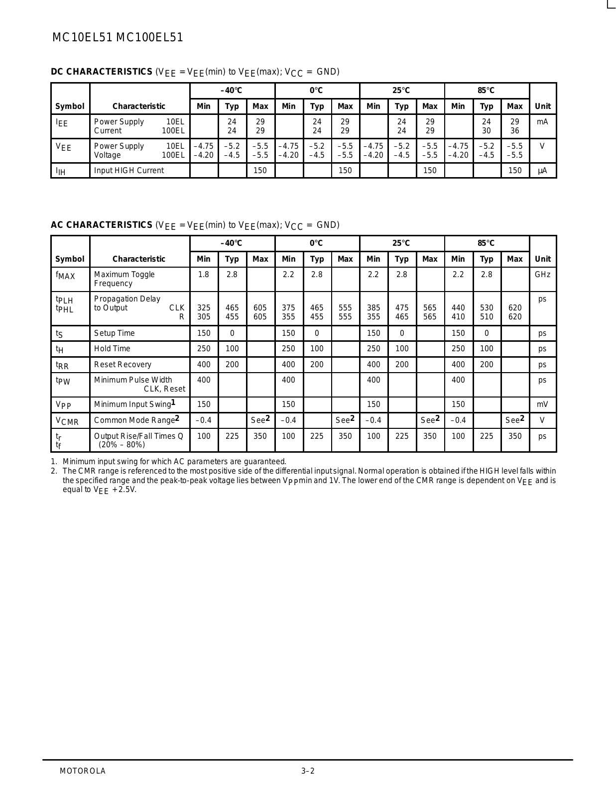
MC10EL51
Technical data
4 pgs
57.07 Kb
0
Table of contents
Loading...
MOTOROLA MC10EL51, MC100EL51 Technical data
...
MOTOROLA Technical data
Download
Specifications and Main Features
Frequently Asked Questions
User Manual
Download
Loading...
+
hidden pages
Unhide
You need points to download manuals.
1 point = 1 manual.
You can buy points or you can get point for every manual you upload.
Buy points
Upload your manuals
 Loading...