


 Loading...
Mitsubishi M30612M8A-XXXGP, M30612M8A-XXXFP, M30612M4A-XXXGP, M30612M4A-XXXFP, M30612E4GP Datasheet
...
|
Mitsubishi microcomputers |
Description |
M16C / 61 Group |
SINGLE-CHIP 16-BIT CMOS MICROCOMPUTER |
|
|
|
|
|
Description
The M16C/61 group of single-chip microcomputers are built using the high-performance silicon gate CMOS process using a M16C/60 Series CPU core and are packaged in a 100-pin plastic molded QFP. These single-chip microcomputers operate using sophisticated instructions featuring a high level of instruction efficiency. With 1M bytes of address space, they are capable of executing instructions at high speed. They also feature a built-in multiplier and DMAC, making them ideal for controlling office, communications, industrial equipment, and other high-speed processing applications.
The M16C/61 group includes a wide range of products with different internal memory types and sizes and various package types.
Features
• Memory capacity ............................................ |
ROM (See Figure 1.1.4. ROM Expansion) |
|
RAM 4K to 10K bytes |
• Shortest instruction execution time ................ |
100ns (f(XIN)=10MHZ) |
• Supply voltage ............................................... |
4.0 to 5.5V (f(XIN)=10MHZ) |
|
2.7 to 5.5V (f(XIN)=7MHZ with software one-wait) |
• Low power consumption ................................ |
18mW ( f(XIN)=7MHZ, with software one-wait, VCC = 3V) |
• Interrupts........................................................ |
20 internal and 5 external interrupt sources, 4 software |
|
interrupt sources; 7 levels (including key input interrupt) |
• Multifunction 16-bit timer ................................ |
5 output timers + 3 input timers |
• Serial I/O (UART or clock synchronous) ........ |
3 channels |
• DMAC ............................................................ |
2 channels (trigger: 16 sources) |
• A-D converter................................................. |
10 bits X 8 channels |
|
(Expandable up to 10 channels) |
• D-A converter................................................. |
8 bits X 2 channels |
• CRC calculation circuit ................................... |
1 circuit |
• Watchdog timer .............................................. |
1 line |
• Programmable I/O ......................................... |
87 lines |
• Input port |
_______ |
1 line (P85 shared with NMI pin) |
|
• Memory expansion ........................................ |
Available (to a maximum of 1M bytes) |
• Chip select output .......................................... |
4 lines |
• Clock generating circuit ................................. |
2 built-in clock generation circuits |
|
(built-in feedback resistor, and external ceramic or quartz oscillator) |
Applications |
|
Audio, cameras, office equipment, communications equipment, portable equipment
------Table of Contents------
Central Processing Unit (CPU) ..................... |
11 |
Reset ............................................................. |
14 |
Processor Mode ............................................ |
19 |
Clock Generating Circuit ............................... |
30 |
Protection ...................................................... |
39 |
Interrupts ....................................................... |
40 |
Watchdog Timer ............................................ |
59 |
DMAC ........................................................... |
61 |
Timer ............................................................. |
70 |
Serial I/O ....................................................... |
87 |
A-D Converter ............................................. |
114 |
D-A Converter ............................................. |
124 |
CRC Calculation Circuit .............................. |
126 |
Programmable I/O Ports ............................. |
128 |
Electrical Characteristics ............................. |
142 |
1
|
Mitsubishi microcomputers |
Description |
M16C / 61 Group |
SINGLE-CHIP 16-BIT CMOS MICROCOMPUTER |
|
|
|
|
|
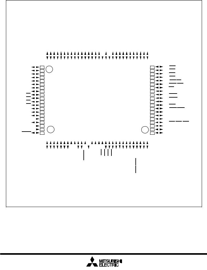
Pin Configuration
Figures 1.1.1 and 1.1.2 show the pin configurations (top view).
PIN CONFIGURATION (top view)
|
|
|
|
|
|
|
|
P1/D08 |
P1/D19 |
P1/D210 |
/DP1311 |
P1/D412 |
P1/D513 |
P1/D614 |
P1/D715 |
P2/A(/D/-)000 |
P2/A(/D/D)1011 |
/A(/D/D)P22122 |
/A(/D/D)P22333 |
/A(/D/D)P24443 |
(/D/D)P2/A5554 |
/D)P2/A(/D6665 |
/D)P2/A(/D7776 |
Vss P3/A(/-/D)087 |
Vcc |
P3/A91 |
P3/A210 |
P3/A311 |
P3/A412 |
/AP3513 |
/AP3614 |
P3/A715 |
P4/A016 |
P4/A117 |
P4/A218 |
P4/A193 |
|
|
||||||||||||||||||||||||||||||||||
|
|
|
|
|
|
|
|
|
|
|
|
|
|
|
|
|
|
|
|
|
|
|
|
|
|
|
|
|
|
|
|
|
|
|
|
|
|
|
|
|
|
|
|
|
|
|
|
|
|
|
|
|
|
|
|
|
|
|
|
|
|
|
|
|
|
|
|
|
|
|
|
|
|
|
|
|
|
|
|
|
|
|
|
|
|
|
|
|
|
|
|
|
|
|
|
|
|
|
|
|
|
|
|
|
|
|
|
|
|
|
|
|
|
|
|
|
|
|
|
|
|
|
|
|
|
|
|
|
|
|
|
|
|
|
|
|
|
|
|
|
|
|
|
|
|
|
|
|
|
|
|
|
80 |
79 |
78 |
77 |
76 |
75 |
74 |
73 |
72 |
71 |
70 |
69 |
68 |
67 |
66 |
65 |
64 |
63 |
62 |
61 |
60 |
59 |
58 |
57 |
56 |
55 |
54 |
53 |
52 |
51 |
|
|
|
|
|
|||||||||||||||||||||||||||||||
P07/D7 |
|
|
|
81 |
|
|
|
|
|
|
|
|
|
|
|
|
|
|
|
|
|
|
|
|
|
|
|
|
|
|
|
|
|
|
|
|
|
|
|
|
|
|
|
|
|
|
|
|
|
|
|
|
|
|
|
|
|
|
|
|
|
|
|
|
|
|
50 |
|
|
P44/CS0 |
||
|
|
|
|
|
|
|
|
|
|
|
|
|
|
|
|
|
|
|
|
|
|
|
|
|
|
|
|
|
|
|
|
|
|
|
|
|
|
|
|
|
|
|
|
|
|
|
|
|
|
|
|
|
|
|
|
|
|
|
|
|
|
|
|
|
|
|
||||||
P06/D6 |
|
|
|
82 |
|
|
|
|
|
|
|
|
|
|
|
|
|
|
|
|
|
|
|
|
|
|
|
|
|
|
|
|
|
|
|
|
|
|
|
|
|
|
|
|
|
|
|
|
|
|
|
|
|
|
|
|
|
|
|
|
|
|
|
|
|
|
49 |
|
|
P45/CS1 |
||
|
|
|
|
|
|
|
|
|
|
|
|
|
|
|
|
|
|
|
|
|
|
|
|
|
|
|
|
|
|
|
|
|
|
|
|
|
|
|
|
|
|
|
|
|
|
|
|
|
|
|
|
|
|
|
|
|
|
|
|
|
|
|
|
|
|
|
||||||
P05/D5 |
|
|
|
83 |
|
|
|
|
|
|
|
|
|
|
|
|
|
|
|
|
|
|
|
|
|
|
|
|
|
|
|
|
|
|
|
|
|
|
|
|
|
|
|
|
|
|
|
|
|
|
|
|
|
|
|
|
|
|
|
|
|
|
|
|
|
|
48 |
|
|
P46/CS2 |
||
|
|
|
|
|
|
|
|
|
|
|
|
|
|
|
|
|
|
|
|
|
|
|
|
|
|
|
|
|
|
|
|
|
|
|
|
|
|
|
|
|
|
|
|
|
|
|
|
|
|
|
|
|
|
|
|
|
|
|
|
|
|
|
|
|
|
|
||||||
P04/D4 |
|
|
|
84 |
|
|
|
|
|
|
|
|
|
|
|
|
|
|
|
|
|
|
|
|
|
|
|
|
|
|
|
|
|
|
|
|
|
|
|
|
|
|
|
|
|
|
|
|
|
|
|
|
|
|
|
|
|
|
|
|
|
|
|
|
|
|
47 |
|
|
P47/CS3 |
||
|
|
|
|
|
|
|
|
|
|
|
|
|
|
|
|
|
|
|
|
|
|
|
|
|
|
|
|
|
|
|
|
|
|
|
|
|
|
|
|
|
|
|
|
|
|
|
|
|
|
|
|
|
|
|
|
|
|
|
|
|
|
|
|
|
|
|
||||||
P03/D3 |
|
|
|
85 |
|
|
|
|
|
|
|
|
|
|
|
|
|
|
|
|
|
|
|
|
|
|
|
|
|
|
|
|
|
|
|
|
|
|
|
|
|
|
|
|
|
|
|
|
|
|
|
|
|
|
|
|
|
|
|
|
|
|
|
|
|
|
46 |
|
|
P50/WRL/WR |
||
|
|
|
|
|
|
|
|
|
|
|
|
|
|
|
|
|
|
|
|
|
|
|
|
|
|
|
|
|
|
|
|
|
|
|
|
|
|
|
|
|
|
|
|
|
|
|
|
|
|
|
|
|
|
|
|
|
|
|
|
|
|
|
|
|
|
|
||||||
P02/D2 |
|
|
|
86 |
|
|
|
|
|
|
|
|
|
|
|
|
|
|
|
|
|
|
|
|
|
|
|
|
|
|
|
|
|
|
|
|
|
|
|
|
|
|
|
|
|
|
|
|
|
|
|
|
|
|
|
|
|
|
|
|
|
|
|
|
|
|
45 |
|
|
P51/WRH/BHE |
||
|
|
|
|
|
|
|
|
|
|
|
|
|
|
|
|
|
|
|
|
|
|
|
|
|
|
|
|
|
|
|
|
|
|
|
|
|
|
|
|
|
|
|
|
|
|
|
|
|
|
|
|
|
|
|
|
|
|
|
|
|
|
|
|
|
|
|||||||
P01/D1 |
|
|
|
87 |
|
|
|
|
|
|
|
|
|
|
|
|
|
|
|
|
|
|
|
|
|
|
|
|
|
|
|
|
|
|
|
|
|
|
|
|
|
|
|
|
|
|
|
|
|
|
|
|
|
|
|
|
|
|
|
|
|
|
|
|
|
|
44 |
|
|
P52/RD |
||
|
|
|
|
|
|
|
|
|
|
|
|
|
|
|
|
|
|
|
|
|
|
|
|
|
|
|
|
|
|
|
|
|
|
|
|
|
|
|
|
|
|
|
|
|
|
|
|
|
|
|
|
|
|
|
|
|
|
|
|
|
|
|
|
|
|
|
||||||
P00/D0 |
|
|
|
88 |
|
|
|
|
|
|
|
|
|
|
|
|
|
|
|
|
|
|
|
|
|
|
|
|
|
|
|
|
|
|
|
|
|
|
|
|
|
|
|
|
|
|
|
|
|
|
|
|
|
|
|
|
|
|
|
|
|
|
|
|
|
|
43 |
|
|
P53/BCLK |
||
|
|
|
|
|
|
|
|
|
|
|
|
|
|
|
|
|
|
|
|
|
|
|
|
|
|
|
|
|
|
|
|
|
|
|
|
|
|
|
|
|
|
|
|
|
|
|
|
|
|
|
|
|
|
|
|
|
|
|
|
|
|
|
|
|
|
|||||||
P107/AN7/KI3 |
89 |
|
|
|
|
|
|
|
|
|
|
|
|
|
M16C/61 Group |
|
|
|
|
|
|
|
|
|
|
|
|
|
42 |
|
|
P54/HLDA |
||||||||||||||||||||||||||||||||||||||||
|
|
|
|
|
|
|
|
|
|
|
|
|
|
|
|
|
|
|
|
|
|
|
|
|
|
|
||||||||||||||||||||||||||||||||||||||||||||||
P106/AN6/KI2 |
|
|
|
|
|
|
|
|
|
|
|
|
|
|
|
|
|
|
|
|
|
|
|
|
|
|
|
|
|
|
|
40 |
|
|
P56/ALE |
|||||||||||||||||||||||||||||||||||||
|
|
|
90 |
|
|
|
|
|
|
|
|
|
|
|
|
|
|
|
|
|
|
|
|
|
|
|
|
|
|
|
|
|
|
|
|
|
|
|
|
|
|
|
|
|
|
|
|
|
|
|
|
|
|
|
|
|
|
|
|
|
|
|
|
|
|
41 |
|
|
P55/HOLD |
|||
P105/AN5/KI1 |
|
|
|
91 |
|
|
|
|
|
|
|
|
|
|
|
|
|
|
|
|
|
|
|
|
|
|
|
|
|
|
|
|
|
|
|
|
|
|
|
|
|
|
|
|
|
|
|
|
|
|
|
|
|
|
|
|
|
|
|
|
|
|
|
|
|
|
|
|
|
|
||
|
|
|
|
|
|
|
|
|
|
|
|
|
|
|
|
|
|
|
|
|
|
|
|
|
|
|
|
|
|
|
|
|
|
|
|
|
|
|
|
|
|
|
|
|
|
|
|
|
|
|
|
|
|
|
|
|
|
|
|
|
|
|
|
|
|
|
||||||
P104/AN4/KI0 |
|
|
|
92 |
|
|
|
|
|
|
|
|
|
|
|
|
|
|
|
|
|
|
|
|
|
|
|
|
|
|
|
|
|
|
|
|
|
|
|
|
|
|
|
|
|
|
|
|
|
|
|
|
|
|
|
|
|
|
|
|
|
|
|
|
|
|
39 |
|
|
P57/RDY/CLKOUT |
||
|
|
|
|
|
|
|
|
|
|
|
|
|
|
|
|
|
|
|
|
|
|
|
|
|
|
|
|
|
|
|
|
|
|
|
|
|
|
|
|
|
|
|
|
|
|
|
|
|
|
|
|
|
|
|
|
|
|
|
|
|
|
|
|
|
||||||||
P103/AN3 |
|
|
|
93 |
|
|
|
|
|
|
|
|
|
|
|
|
|
|
|
|
|
|
|
|
|
|
|
|
|
|
|
|
|
|
|
|
|
|
|
|
|
|
|
|
|
|
|
|
|
|
|
|
|
|
|
|
|
|
|
|
|
|
|
|
|
|
38 |
|
|
P60/CTS0/RTS0 |
||
|
|
|
|
|
|
|
|
|
|
|
|
|
|
|
|
|
|
|
|
|
|
|
|
|
|
|
|
|
|
|
|
|
|
|
|
|
|
|
|
|
|
|
|
|
|
|
|
|
|
|
|
|
|
|
|
|
|
|
|
|
|
|
|
|
||||||||
P102/AN2 |
|
|
|
94 |
|
|
|
|
|
|
|
|
|
|
|
|
|
|
|
|
|
|
|
|
|
|
|
|
|
|
|
|
|
|
|
|
|
|
|
|
|
|
|
|
|
|
|
|
|
|
|
|
|
|
|
|
|
|
|
|
|
|
|
|
|
|
37 |
|
|
P61/CLK0 |
||
|
|
|
|
|
|
|
|
|
|
|
|
|
|
|
|
|
|
|
|
|
|
|
|
|
|
|
|
|
|
|
|
|
|
|
|
|
|
|
|
|
|
|
|
|
|
|
|
|
|
|
|
|
|
|
|
|
|
|
|
|
|
|
|
|
||||||||
P101/AN1 |
|
|
|
95 |
|
|
|
|
|
|
|
|
|
|
|
|
|
|
|
|
|
|
|
|
|
|
|
|
|
|
|
|
|
|
|
|
|
|
|
|
|
|
|
|
|
|
|
|
|
|
|
|
|
|
|
|
|
|
|
|
|
|
|
|
|
|
36 |
|
|
P62/RxD0 |
||
|
|
|
|
|
|
|
|
|
|
|
|
|
|
|
|
|
|
|
|
|
|
|
|
|
|
|
|
|
|
|
|
|
|
|
|
|
|
|
|
|
|
|
|
|
|
|
|
|
|
|
|
|
|
|
|
|
|
|
|
|
|
|
|
|
||||||||
AVSS |
|
|
|
96 |
|
|
|
|
|
|
|
|
|
|
|
|
|
|
|
|
|
|
|
|
|
|
|
|
|
|
|
|
|
|
|
|
|
|
|
|
|
|
|
|
|
|
|
|
|
|
|
|
|
|
|
|
|
|
|
|
|
|
|
|
|
|
35 |
|
|
P63/TXD0 |
||
|
|
|
|
|
|
|
|
|
|
|
|
|
|
|
|
|
|
|
|
|
|
|
|
|
|
|
|
|
|
|
|
|
|
|
|
|
|
|
|
|
|
|
|
|
|
|
|
|
|
|
|
|
|
|
|
|
|
|
|
|
|
|
|
|
|
|||||||
P100/AN0 |
|
|
97 |
|
|
|
|
|
|
|
|
|
|
|
|
|
|
|
|
|
|
|
|
|
|
|
|
|
|
|
|
|
|
|
|
|
|
|
|
|
|
|
|
|
|
|
|
|
|
|
|
|
|
|
|
|
|
|
|
|
|
|
|
|
|
34 |
|
|
P64/CTS1/RTS1/CTS0/CLKS1 |
|||
|
|
|
|
|
|
|
|
|
|
|
|
|
|
|
|
|
|
|
|
|
|
|
|
|
|
|
|
|
|
|
|
|
|
|
|
|
|
|
|
|
|
|
|
|
|
|
|
|
|
|
|
|
|
|
|
|
|
|
|
|
|
|
|
|
||||||||
VREF |
|
|
|
98 |
|
|
|
|
|
|
|
|
|
|
|
|
|
|
|
|
|
|
|
|
|
|
|
|
|
|
|
|
|
|
|
|
|
|
|
|
|
|
|
|
|
|
|
|
|
|
|
|
|
|
|
|
|
|
|
|
|
|
|
|
|
|
33 |
|
|
P65/CLK1 |
||
|
|
|
|
|
|
|
|
|
|
|
|
|
|
|
|
|
|
|
|
|
|
|
|
|
|
|
|
|
|
|
|
|
|
|
|
|
|
|
|
|
|
|
|
|
|
|
|
|
|
|
|
|
|
|
|
|
|
|
|
|
|
|
|
|
|
|
||||||
AVcc |
|
|
|
|
99 |
|
|
|
|
|
|
|
|
|
|
|
|
|
|
|
|
|
|
|
|
|
|
|
|
|
|
|
|
|
|
|
|
|
|
|
|
|
|
|
|
|
|
|
|
|
|
|
|
|
|
|
|
|
|
|
|
|
|
|
|
|
|
32 |
|
|
P66/RxD1 |
|
|
|
|
|
|
|
|
|
|
|
|
|
|
|
|
|
|
|
|
|
|
|
|
|
|
|
|
|
|
|
|
|
|
|
|
|
|
|
|
|
|
|
|
|
|
|
|
|
|
|
|
|
|
|
|
|
|
|
|
|
|
|
|
|
|
|
|
|
|||||
P97/ADTRG |
|
|
100 |
|
|
|
|
|
|
|
|
|
|
|
|
|
|
|
|
|
|
|
|
|
|
|
|
|
|
|
|
|
|
|
|
|
|
|
|
|
|
|
|
|
|
|
|
|
|
|
|
|
|
|
|
|
|
|
|
|
|
|
|
|
|
31 |
|
|
P67/TXD1 |
|||
|
|
|
|
|
|
|
|
|
|
|
|
|
|
|
|
|
|
|
|
|
|
|
|
|
|
|
|
|
|
|
|
|
|
|
|
|
|
|
|
|
|
|
|
|
|
|
|
|
|
|
|
|
|
|
|
|
|
|
|
|
|
|
|
|
||||||||
|
|
|
|
|
|
|
|
|
|
|
|
|
|
|
|
|
|
|
|
|
|
|
|
|
|
|
|
|
|
|
|
|
|
|
|
|
|
|
|
|
|
|
|
|
|
|
|
|
|
|
|
|
|
|
|
|
|
|
|
|
|
|
|
|
|
|
|
|
|
|
|
|
|
|
|
|
|
|
|
1 |
2 |
3 |
4 |
5 |
6 |
7 |
8 |
9 |
10 |
11 |
12 |
13 |
14 |
15 |
16 |
17 |
18 |
19 |
20 |
21 |
22 |
23 |
24 |
25 |
26 |
27 |
28 |
29 |
30 |
|
|
|
|
|
|||||||||||||||||||||||||||||||
|
|
|
|
|
|
|
|
|
|
|
|
|
|
|
|
|
|
|
|
|
|
|
|
|
|
|
|
|
|
|
|
|
|
|
|
|
|
|
|
|
|
|
|
|
|
|
|
|
|
|
|
|
|
|
|
|
|
|
|
|
|
|
|
|
|
|
|
|
|
|||
|
|
|
|
|
|
|
|
|
|
|
|
|
|
|
|
|
|
|
|
|
|
|
|
|
|
|
|
|
|
|
|
|
|
|
|
|
|
|
|
|
|
|
|
|
|
|
|
|
|
|
|
|
|
|
|
|
|
|
|
|
|
|
|
|
|
|
|
|
|
|
||
|
|
|
|
|
|
|
|
P9/ANEX16 |
P9/ANEX05 |
P9/DA41 |
/DAP930 |
P9/TB2IN2 |
P9/TB11IN |
P9/TB00IN |
BYTE |
CNVss |
P8/X7CIN |
P8/X6COUT |
RESET |
XOUT |
VSS |
XIN |
VCC |
P8/NMI5 |
P8/INT24 |
P8/INT31 |
P8/INT20 |
P8/TA41IN |
/TA4P80OUT |
P7/TA3IN7 |
P7/TA36OUT |
P7/TA25IN |
P7/TA24OUT |
/RTS/TA1P7/CTS322IN |
P7/CLK/TA1OUT22 |
(Note)P7/RxD/TA012IN |
/TxD/TA0(Note)P702OUT |
|
|
|||||||||||||||||||||||||||||||||
|
|
|
|
|
|
|
|
|
|
|
|
|
|
|
|
|
|
|
|
|
|
|
|
|
|
|
|
|
|
|
|
|
|
|
|
|
|
|
|
|
|
|
|
|
|
|
|
|
|
|
|
|
|
|
|
|
|
|
|
|
|
|
|
|
|
|
|
|
Package: 100P6S-A |
|||
Note: P70 and P71 are N channel open-drain output pin.
Figure 1.1.1. Pin configuration (top view)
2
|
Mitsubishi microcomputers |
Description |
M16C / 61 Group |
SINGLE-CHIP 16-BIT CMOS MICROCOMPUTER |
|
|
|
|
|
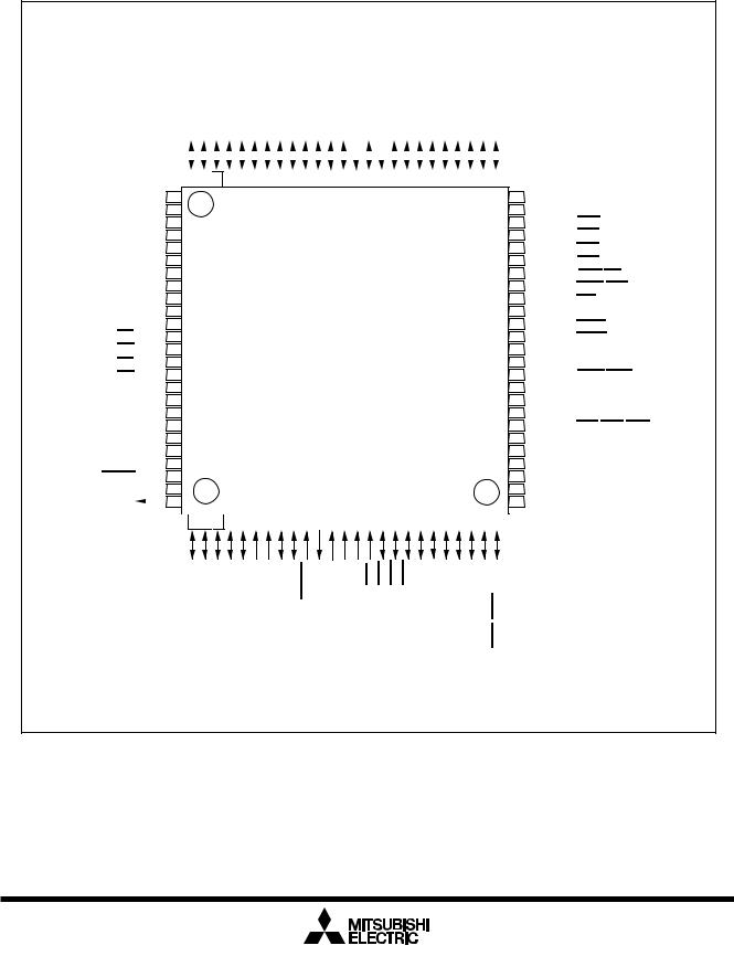
PIN CONFIGURATION (top view)
P1/D311 |
P1/D412 |
P1/D513 |
|||
|
|
|
|
|
|
|
|
|
|
73 |
|
75 |
74 |
||||
P12/D10
 76
76
P11/D9
 77
77
P10/D8 
 78
78
P07/D7
 79
79
P06/D6
 80
80
P05/D5
 81
81
P04/D4
 82
82
P03/D3
 83
83
P02/D2
 84
84
P01/D1
 85
85
P00/D0
 86
86
P107/AN7/KI3 
 87
87
P106/AN6/KI2 
 88
88
P105/AN5/KI1 
 89
89
P104/AN4/KI0
 90
90
P103/AN3
 91
91
P102/AN2
 92
92
P101/AN1
 93
93
AVSS  94
94
P100/AN0
 95
95
VREF  96
96
AVcc 97
97
P97/ADTRG
 98
98
P96/ANEX1
 99
99
P95/ANEX0  100
100
1
 2
2
 3
3
/DA1 /DA0 /TB2IN P94 P93 2 P9
P1/D614 |
P1/D715 |
P2/A(/D/-)000 |
)P2/A(/D/D1110 |
/A(/D/D)P22221 |
/A(/D/D)P23332 |
P2/A(/D/D)4344 |
/A(/D/D)P25554 |
/D)P2/A(/D6665 |
P2/A(/D/D)6777 |
Vss |
(/-/D)P3/A087 |
Vcc |
/AP319 |
P3/A210 |
P3/A311 |
/AP3412 |
P3/A135 |
P3/A614 |
P3/A715 |
P4/A016 |
P4/A117 |
||||||||||||||||||||||
|
|
|
|
|
|
|
|
|
|
|
|
|
|
|
|
|
|
|
|
|
|
|
|
|
|
|
|
|
|
|
|
|
|
|
|
|
|
|
|
|
|
|
|
|
|
|
|
|
|
|
|
|
|
|
|
|
|
|
|
|
|
|
|
|
|
|
|
|
|
|
|
|
|
|
|
|
|
|
|
|
|
|
|
|
|
|
|
72 |
71 |
70 |
69 |
68 |
67 |
66 |
65 |
64 |
63 |
62 |
61 |
60 |
59 |
58 |
57 |
56 |
55 |
54 |
53 |
52 |
51 |
||||||||||||||||||||||
M16C/61 Group
4 |
5 |
6 |
7 |
8 |
9 |
10 |
11 |
12 |
13 |
14 |
15 |
16 |
17 |
18 |
19 |
20 |
21 |
22 |
23 |
24 |
25 |
P9/TB11IN |
P9/TB00IN |
BYTE CNVss P8/X7CIN |
P8/X6COUT |
RESET XOUT |
VSS |
XIN |
VCC |
P8/NMI5 |
/INTP842 |
P8/INT31 |
P8/INT20 |
P8/TA41IN |
P8/TA40OUT |
P7/TA37IN |
P7/TA36OUT |
P7/TA2IN5 |
/TA2P74OUT |
/RTS/TA1IN2 |
|
|
|
|
|
|
|
|
|
|
|
|
|
|
|
|
|
|
P7/CTS32 |
50 
 P42/A18
49 
 P43/A19
48 
 P44/CS0
47 
 P45/CS1
46 
 P46/CS2
45 
 P47/CS3
44 
 P50/WRL/WR
43 
 P51/WRH/BHE
42 
 P52/RD
41 
 P53/BCLK
40 
 P54/HLDA
39 
 P55/HOLD
38 
 P56/ALE
37 
 P57/RDY/CLKOUT
36 
 P60/CTS0/RTS0 35
 P61/CLK0
34 
 P62/RxD0
33 
 P63/TXD0
32 
 P64/CTS1/RTS1/CTS0/CLKS1
31 
 P65/CLK1
30 
 P66/RxD1
29 
 P67/TXD1
28 
 P70/TxD2/TA0OUT(Note)
27 
 P71/RxD2/TA0IN(Note)
26 
 P72/CLK2/TA1OUT
Package: 100P6Q-A
Note: P70 and P71 are N channel open-drain output pin.
Figure 1.1.2. Pin configuration (top view)
3

|
Mitsubishi microcomputers |
Description |
M16C / 61 Group |
SINGLE-CHIP 16-BIT CMOS MICROCOMPUTER |
|
|
|
|
|
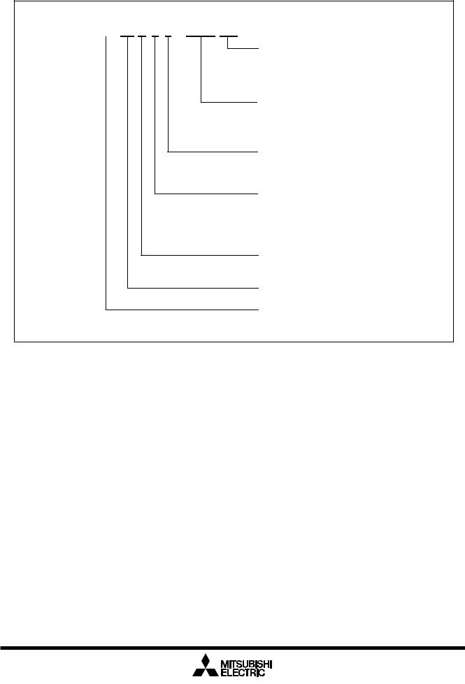
Block Diagram
Figure 1.1.3 is a block diagram of the M16C/61 group.
Block diagram of the M16C/61 group
I/O ports
|
8 |
|
8 |
8 |
|
8 |
|
8 |
|
|
8 |
|
8 |
||||||
|
|
|
|
|
|
|
|
||||||||||||
|
|
|
|
|
|
|
|
|
|
|
|
|
|
|
|
|
|
|
|
Port P0 |
|
Port P1 |
|
Port P2 |
|
Port P3 |
|
Port P4 |
|
Port P5 |
|
Port P6 |
|||||||
Internal peripheral functions |
A-D converter |
System clock generator |
|||
|
|||||
Timer |
(10 bits X 8 channels |
|
XIN-XOUT |
||
Timer TA0 (16 bits) |
Expandable up to 10 channels) |
XCIN-XCOUT |
|||
|
|
|
|
|
|
Timer TA1 (16 bits) |
|
|
|
|
|
Timer TA2 (16 bits) |
UART/clock synchronous SI/O |
|
|||
Timer TA3 (16 bits) |
(8 bits X 3channels) (Note 3) |
|
|||
|
|
|
|
|
|
Timer TA4 (16 bits) |
CRC arithmetic circuit (CCITT ) |
|
|||
Timer TB0 (16 bits) |
|
||||
Timer TB1 (16 bits) |
(Polynomial : X16+X12+X5+1) |
|
|||
|
|
|
|
|
|
Timer TB2 (16 bits) |
M16C/60 series16-bit CPU core |
Memory |
|||
|
|||||
|
Registers |
Program counter |
ROM |
||
Watchdog timer |
|
|
(Note 1) |
||
R0H |
R0L |
|
PC |
||
(15 bits) |
R0H |
R0L |
|
|
RAM |
R1H |
R1L |
|
|
||
|
R1H |
R1L |
|
Vector table |
(Note 2) |
|
R2 |
|
|||
DMAC |
|
R2 |
|
INTB |
|
|
R3 |
|
|
||
|
R3 |
|
|
|
|
(2 channels) |
A0 |
|
Stack pointer |
|
|
|
A0 |
|
|
||
|
A1 |
|
|
|
|
|
|
A1 |
|
ISP |
|
D-A converter |
FB |
|
|
||
|
FB |
|
USP |
Multiplier |
|
(8 bits X 2 channels) |
|
|
|
||
|
|
|
|
||
|
|
SB |
|
FLG |
|
Note 1: ROM size depends on MCU type.
Note 2: RAM size depends on MCU type.
Note 3: One of serial I/O can use for SIM interface.
P7Port |
|
8 |
|
P8Port |
|
7 |
|
5P8Port |
|
|
|
P9Port |
|
8 |
|
P10Port |
|
8 |
Figure 1.1.3. Block diagram of M16C/61 group
4

|
Mitsubishi microcomputers |
Description |
M16C / 61 Group |
SINGLE-CHIP 16-BIT CMOS MICROCOMPUTER |
|
|
|
|
|
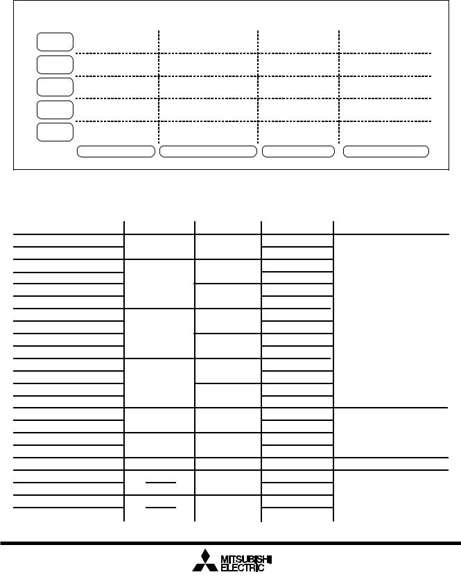
Performance Outline
Table 1.1.1 is a performance outline of M16C/61 group.
Table 1.1.1. Performance outline of M16C/61 group
|
|
Item |
Performance |
|
|
|
|
Number of basic instructions |
91 instructions |
||
|
|
|
|
Shortest instruction execution time |
100ns(f(XIN)=10MHZ) |
||
|
|
|
|
Memory |
|
ROM |
(See the Figure 4. ROM Expansion) |
|
|
|
|
capacity |
|
RAM |
4K to 10K bytes |
|
|
|
|
I/O port |
|
P0 to P10 (except P85) |
8 bits x 10, 7 bits x 1 |
|
|
|
|
Input port |
|
P85 |
1 bit x 1 |
|
|
|
|
Multifunction |
|
TA0, TA1, TA2, TA3, TA4 |
16 bits x 5 |
|
|
|
|
timer |
|
TB0, TB1, TB2 |
16 bits x 3 |
|
|
|
|
Serial I/O |
|
UART0, UART1, UART2 |
(UART or clock synchronous) x 3 |
|
|
|
|
A-D converter |
|
10 bits x (8 + 2) channels |
|
|
|
|
|
D-A converter |
|
8 bits x 2 |
|
|
|
|
|
DMAC |
|
2 channels (trigger: 16 sources) |
|
|
|
|
|
CRC calculation circuit |
CRC - CCITT |
||
|
|
|
|
Watchdog timer |
|
15 bits x 1 (with prescaler) |
|
|
|
|
|
Interrupt |
|
20 internal and 5 external sources, 4 software sources, 7 levels |
|
|
|
|
|
Clock generating circuit |
2 built-in clock generation circuits |
||
|
|
|
(built-in feedback resistor, and external ceramic or quartz oscillator) |
|
|
|
|
Supply voltage |
|
4.0 to 5.5V (f(XIN ) = 10MHZ) |
|
|
|
|
2.7 to 5.5V(f(XIN)=7MHZ with software one-wait) |
|
|
|
|
Power consumption |
|
18mW (f(XIN) = 7MHZ with software one-wait,VCC = 3V) |
|
|
|
|
|
I/O |
|
I/O withstand voltage |
5V |
characteristics |
|
|
|
|
Output current |
5mA |
|
|
|
|
|
Memory expansion |
|
Available (to a maximum of 1M bytes) |
|
|
|
|
|
Device configuration |
|
CMOS silicon gate |
|
|
|
|
|
Package |
|
100-pin plastic mold QFP |
|
|
|
|
|
5
|
Mitsubishi microcomputers |
Description |
M16C / 61 Group |
SINGLE-CHIP 16-BIT CMOS MICROCOMPUTER |
|
|
|
|
|
Mitsubishi plans to release the following products in the M16C/61 group:
(1)Support for mask ROM version, external ROM version, one-time PROM version, and EPROM version
(2)ROM capacity
(3)Package
100P6S-A : Plastic molded QFP (mask ROM version and one-time PROM version) 100P6Q-A : Plastic molded QFP (mask ROM version and one-time PROM version) 100D0 : Ceramic LCC (EPROM version)
ROM |
|
|
|
|
Size(Byte) |
|
|
|
|
External |
|
|
|
M30612SAFP/GP |
ROM |
|
|
|
M30610SAFP/GP |
128 K |
M30610MCA-XXXFP/GP |
M30610ECFP/GP |
M30610ECFS |
|
M30612MCA-XXXFP/GP |
|
|||
|
|
|
|
|
96 K |
M30610MAA-XXXFP/GP |
|
|
|
M30612MAA-XXXFP/GP |
|
|
|
|
64 K |
M30610M8A-XXXFP/GP |
|
|
|
M30612M8A-XXXFP/GP |
|
|
|
|
|
|
|
|
|
32 K |
M30612M4A-XXXFP/GP |
M30612E4FP/GP |
|
|
|
Mask ROM version |
One-time PROM version |
EPROM version |
External ROM version |
Figure 1.1.4. ROM expansion
The M16C/61 group products currently supported are listed in Table 2.
Table 1.1.2. M16C/61 group |
|
|
Apr. 1999 |
||
Type No |
ROM capacity |
RAM capacity |
Package type |
Remarks |
|
M30612M4A-XXXFP |
32K byte |
4K byte |
100P6S-A |
|
|
|
|||||
M30612M4A-XXXGP |
100P6Q-A |
|
|||
|
|||||
|
|
|
|||
M30610M8A-XXXFP |
|
10K byte |
100P6S-A |
|
|
|
|
||||
M30610M8A-XXXGP |
64K byte |
100P6Q-A |
|
||
|
|||||
|
|
||||
M30612M8A-XXXFP |
4K byte |
100P6S-A |
|
||
|
|||||
|
|
||||
M30612M8A-XXXGP |
|
100P6Q-A |
|
||
|
|
||||
|
|
|
|||
M30610MAA-XXXFP |
|
10K byte |
100P6S-A |
|
|
|
|
||||
M30610MAA-XXXGP |
96K byte |
100P6Q-A |
Mask ROM version |
||
|
|||||
M30612MAA-XXXFP |
4K byte |
100P6S-A |
|||
|
|
||||
M30612MAA-XXXGP |
|
100P6Q-A |
|
||
|
|
||||
|
|
|
|||
M30610MCA-XXXFP |
|
10K byte |
100P6S-A |
|
|
|
|
||||
M30610MCA-XXXGP |
128K byte |
100P6Q-A |
|
||
|
|||||
|
|
||||
M30612MCA-XXXFP |
5K byte |
100P6S-A |
|
||
|
|||||
|
|
||||
M30612MCA-XXXGP |
|
100P6Q-A |
|
||
|
|
||||
|
|
|
|||
M30612E4FP |
32K byte |
4K byte |
100P6S-A |
|
|
|
|||||
M30612E4GP |
100P6Q-A |
One-time PROM version |
|||
|
|
||||
M30610ECFP |
128K byte |
10K byte |
100P6S-A |
||
|
|||||
M30610ECGP |
100P6Q-A |
|
|||
|
|||||
|
|
|
|||
M30610ECFS |
128K byte |
10K byte |
100D0 |
EPROM version (Note) |
|
M30610SAFP |
|
10K byte |
100P6S-A |
|
|
|
|
||||
M30610SAGP |
|
100P6Q-A |
External ROM version |
||
|
|||||
|
|
||||
M30612SAFP |
|
4K byte |
100P6S-A |
||
|
|||||
|
|
||||
M30612SAGP |
|
100P6Q-A |
|
||
|
|
||||
|
|
|
|||
|
|
|
|
|
|
Note: Do not use the EPROM version for mass production, because it is a tool for program development (for evaluation).
6
|
Mitsubishi microcomputers |
Description |
M16C / 61 Group |
SINGLE-CHIP 16-BIT CMOS MICROCOMPUTER |
|
|
|
|
|
Type No. M 3 0 6 1 2 M 4 – X X X F P
Package type: |
|
|
FP |
: Package |
100P6S-A |
GP |
: |
100P6Q-A |
FS |
: |
100D0 |
ROM No.
Omitted for blank one-time PROM version and EPROM version
ROM capacity: |
|
4 : 32K bytes |
A : 96K bytes |
8 : 64K bytes |
C : 128K bytes |
Memory type:
M : Mask ROM version
E : EPROM or one-time PROM version
S : External ROM version
Shows RAM capacity, pin count, etc (The value itself has no specific meaning)
M16C/61 Group
M16C Family
Figure 1.1.5. Type No., memory size, and package
7
Mitsubishi microcomputers
M16C / 61 Group
Pin Description |
SINGLE-CHIP 16-BIT CMOS MICROCOMPUTER |
|
|
|
|
Pin Description
Pin name |
Signal name |
I/O type |
VCC, VSS |
Power supply |
|
|
input |
|
CNVSS |
CNVSS |
Input |
RESET |
Reset input |
Input |
XIN |
Clock input |
Input |
XOUT |
Clock output |
Output |
BYTE |
External data |
Input |
|
bus width |
|
|
select input |
|
AVCC |
Analog power |
|
|
supply input |
|
AVSS |
Analog power |
|
|
supply input |
|
VREF |
Reference |
Input |
|
voltage input |
|
P00 to P07 |
I/O port P0 |
Input/output |
|
D0 to D7 |
|
Input/output |
|
P10 to P17 |
I/O port P1 |
Input/output |
|
D8 to D15 |
|
Input/output |
|
P20 to P27 |
I/O port P2 |
Input/output |
|
A0 to A7 |
|
Output |
|
A0/D0 to |
|
Input/output |
|
A7/D7 |
|
|
|
A0, A1/D0 |
|
Output |
|
to A7/D6 |
|
Input/output |
|
P30 to P37 |
I/O port P3 |
Input/output |
|
A8 to A15 |
|
Output |
|
A8/D7, |
|
Input/output |
|
A9 to A15 |
|
Output |
|
P40 to P47 |
I/O port P4 |
Input/output |
|
|||
|
CS0 to CS3, |
|
Output |
|
A16 to A19 |
|
Output |
|
|
|
|
Function
Supply 2.7 to 5.5 V to the VCC pin. Supply 0 V to the VSS pin.
This pin switches between processor modes. Connect it to the VSS pin when operating in single-chip or memory expansion mode. Connect it to the VCC pin when in microprocessor mode.
A “L” on this input resets the microcomputer.
These pins are provided for the main clock generating circuit.Connect a ceramic resonator or crystal between the XIN and the XOUT pins. To use an externally derived clock, input it to the XIN pin and leave the XOUT pin open.
This pin selects the width of an external data bus. A 16-bit width is selected when this input is “L”; an 8-bit width is selected when this input is “H”. This input must be fixed to either “H” or “L”. When operating in single-chip mode,connect this pin to VSS.
This pin is a power supply input for the A-D converter. Connect this pin to VCC.
This pin is a power supply input for the A-D converter. Connect this pin to VSS.
This pin is a reference voltage input for the A-D converter.
This is an 8-bit CMOS I/O port. It has an input/output port direction register that allows the user to set each pin for input or output individually. When used for input in single-chip mode, the port can be set to have or not have a pull-up resistor in units of four bits by software. In memory expansion and microprocessor modes, selection of the internal pull-resistor is not available.
When set as a separate bus, these pins input and output data (D0–D7).
This is an 8-bit I/O port equivalent to P0.
When set as a separate bus, these pins input and output data (D8–D15).
This is an 8-bit I/O port equivalent to P0.
These pins output 8 low-order address bits (A0–A7).
If the external bus is set as an 8-bit wide multiplexed bus, these pins input and output data (D0–D7) and output 8 low-order address bits (A0–A7) separated in time by multiplexing.
If the external bus is set as a 16-bit wide multiplexed bus, these pins input and output data (D0–D6) and output address (A1–A7) separated in time by multiplexing. They also output address (A0).
This is an 8-bit I/O port equivalent to P0.
These pins output 8 middle-order address bits (A8–A15).
If the external bus is set as a 16-bit wide multiplexed bus, these pins input and output data (D7) and output address (A8) separated in time by multiplexing. They also output address (A9–A15).
This is an 8-bit I/O port equivalent to P0.
These pins output CS0–CS3 signals and A16–A19. CS0–CS3 are chip select signals used to specify an access space. A16–A19 are 4 highorder address bits.
8
|
Mitsubishi microcomputers |
Pin Description |
M16C / 61 Group |
SINGLE-CHIP 16-BIT CMOS MICROCOMPUTER |
|
|
|
|
|
Pin Description
Pin name |
Signal name |
I/O type |
P50 to P57 |
I/O port P5 |
Input/output |
WRL / WR, |
|
Output |
WRH / BHE, |
|
Output |
RD, |
|
Output |
BCLK, |
|
Output |
HLDA, |
|
Output |
HOLD, |
|
Input |
ALE, |
|
Output |
RDY |
|
Input |
P60 to P67 |
I/O port P6 |
Input/output |
P70 to P77 |
I/O port P7 |
Input/output |
P80 to P84, |
I/O port P8 |
Input/output |
P86, |
|
Input/output |
P87, |
|
Input/output |
P85 |
I/O port P85 |
Input |
P90 to P97 |
I/O port P9 |
Input/output |
P100 to P107 |
I/O port P10 |
Input/output |
Function
This is an 8-bit I/O port equivalent to P0. In single-chip mode, P57 in this port outputs a divide-by-8 or divide-by-32 clock of XIN or a clock of the same frequency as XCIN as selected by software.
Output WRL, WRH (WR and BHE), RD, BCLK, HLDA, and ALE signals. WRL and WRH, and BHE and WR can be switched using software control.

 WRL, WRH, and RD selected
With a 16-bit external data bus, data is written to even addresses when the WRL signal is “L” and to the odd addresses when the WRH signal is “L”. Data is read when RD is “L”.

 WR, BHE, and RD selected
Data is written when WR is “L”. Data is read when RD is “L”. Odd addresses are accessed when BHE is “L”. Use this mode when using an 8-bit external data bus.
While the input level at the HOLD pin is “L”, the microcomputer is placed in the hold state. While in the hold state, HLDA outputs a “L” level. ALE is used to latch the address. While the input level of the RDY pin is “L”, the microcomputer is in the ready state.
This is an 8-bit I/O port equivalent to P0. When used for input in singlechip, memory expansion, and microprocessor modes, the port can be set to have or not have a pull-up resistor in units of four bits by software. Pins in this port also function as UART0 and UART1 I/O pins as selected by software.
This is an 8-bit I/O port equivalent to P6 (P70 and P71 are N channel open-drain output). Pins in this port also function as timer A0–A3 or UART2 I/O pins as selected by software.
P80 to P84, P86, and P87 are I/O ports with the same functions as P6. Using software, they can be made to function as the I/O pins for timer A4 and the input pins for external interrupts. P86 and P87 can be set using software to function as the I/O pins for a sub clock generation circuit. In this case, connect a quartz oscillator between P86 (XCOUT pin) and P87 (XCIN pin). P85 is an input-only port that also functions for NMI. The NMI interrupt is generated when the input at this pin
changes from “H” to “L”. The NMI function cannot be cancelled using software. The pull-up cannot be set for this pin.
This is an 8-bit I/O port equivalent to P6. Pins in this port also function as Timer B0–B2 input pins, D-A converter output pins, A-D converter extended input pins, or A-D trigger input pins as selected by software.
This is an 8-bit I/O port equivalent to P6. Pins in this port also function as A-D converter input pins. Furthermore, P104–P107 also function as input pins for the key input interrupt function.
9
|
Mitsubishi microcomputers |
Memory |
M16C / 61 Group |
SINGLE-CHIP 16-BIT CMOS MICROCOMPUTER |
|
|
|
|
|
Operation of Functional Blocks
The M16C/61 group accommodates certain units in a single chip. These units include ROM and RAM to store instructions and data and the central processing unit (CPU) to execute arithmetic/logic operations. Also included are peripheral units such as timers, serial I/O, D-A converter, DMAC, CRC calculation circuit, A-D converter, and I/O ports.
The following explains each unit.
Memory
Figure 1.4.1 is a memory map of the M16C/61 group. The address space extends the 1M bytes from address 0000016 to FFFFF16. From FFFFF16 down is ROM. For example, in the M30612M4A-XXXFP,
there is 32K bytes of internal ROM from F800016 to FFFFF16. The vector table for fixed interrupts such as
_______
the reset and NMI are mapped to FFFDC16 to FFFFF16. The starting address of the interrupt routine is stored here. The address of the vector table for timer interrupts, etc., can be set as desired using the internal register (INTB). See the section on interrupts for details.
From 0040016 up is RAM. For example, in the M30612M4A-XXXFP, 4K bytes of internal RAM is mapped to the space from 0040016 to 013FF16. In addition to storing data, the RAM also stores the stack used when calling subroutines and when interrupts are generated.
The SFR area is mapped to 0000016 to 003FF16. This area accommodates the control registers for peripheral devices such as I/O ports, A-D converter, serial I/O, and timers, etc. Any part of the SFR area that is not occupied is reserved and cannot be used for other purposes.
The special page vector table is mapped to FFE0016 to FFFDB16. If the starting addresses of subroutines or the destination addresses of jumps are stored here, subroutine call instructions and jump instructions can be used as 2-byte instructions, reducing the number of program steps.
In memory expansion mode and microprocessor mode, a part of the spaces are reserved and cannot be used. For example, in the M30612M4A-XXXFP, the following spaces cannot be used.
•The space between 0140016 and 03FFF16
•The space between D000016 and F7FFF16 (When external area do not expand in memory expansion mode)
Do not expand the external area in single chip mode. A part of internal memory cannot be used depending
on MCU.
0000016
SFR area
For details, see Figure
1.7.1 and Figure 1.7.2
FFE0016
0040016
|
|
|
|
Internal RAM area |
|
|
Special page |
|
|
|
|
XXXXX16 |
|
|
|
|
|
|
|
|
|
|
|
|
vector table |
|
|
|
|
|
Internal reserved |
|
|
||
|
|
|
|
|
|
|
||
|
|
|
|
area (Note 1) |
|
|
|
|
|
|
|
0400016 |
|
|
FFFDC16 |
|
Undefined instruction |
|
|
|
External area |
|
||||
|
|
|
|
|
||||
|
|
|
|
|
|
|||
|
|
|
|
|
|
|
|
Overflow |
Type No. |
Address XXXXX16 |
Address YYYYY16 |
|
|
|
|
|
BRK instruction |
M30610M8A |
02BFF16 |
F000016 |
D000016 |
|
|
|
|
Address match |
Internal reserved |
|
|||||||
M30610MAA |
02BFF16 |
E800016 |
|
|
Single step |
|||
|
area (Note 2) |
|
|
|||||
M30610MCA/EC |
02BFF16 |
E000016 |
YYYYY16 |
|
|
|
|
Watchdog timer |
M30612M4A/E4 |
013FF16 |
F800016 |
|
Internal ROM area |
|
|
DBC |
|
M30612M8A |
013FF16 |
F000016 |
|
|
|
|||
|
|
|
||||||
|
|
|
NMI |
|||||
M30612MAA |
013FF16 |
E800016 |
|
|
|
|
|
|
|
|
|
|
|
Reset |
|||
M30612MCA |
017FF16 |
E000016 |
FFFFF16 |
|
|
FFFFF16 |
|
|
|
|
|
||||||
Note 1: During memory expansion and microprocessor modes, can not be used.
Note 2: When external area do not expand in memory expansion mode.
Figure 1.4.1. Memory map
10
|
Mitsubishi microcomputers |
CPU |
M16C / 61 Group |
SINGLE-CHIP 16-BIT CMOS MICROCOMPUTER |
|
|
|
|
|
Central Processing Unit (CPU)
The CPU has a total of 13 registers shown in Figure 1.5.1. Seven of these registers (R0, R1, R2, R3, A0, A1, and FB) come in two sets; therefore, these have two register banks.
|
b15 |
|
b8 b7 |
|
|
b0 |
|
|||
R0(Note) |
|
|
|
H |
|
|
L |
|
||
|
|
|
|
|
|
|||||
|
b15 |
|
b8 b7 |
|
|
b0 |
|
|||
R1(Note) |
|
|
|
|
|
|
|
|
|
|
|
|
|
H |
|
|
L |
|
|||
|
|
|
|
|||||||
b15 |
|
|
|
|
|
b0 |
|
|||
R2(Note) |
|
|
|
|
|
|
|
|
|
|
|
|
|
|
|
|
|
|
|
||
b15 |
|
|
|
|
|
b0 |
|
|||
R3(Note) |
|
|
|
|
|
|
|
|
|
|
|
|
|
|
|
|
|
|
|
|
|
b15 |
|
|
|
|
|
b0 |
|
|||
A0(Note) |
|
|
|
|
|
|
|
|
|
|
|
|
|
|
|
|
|
|
|
||
b15 |
|
|
|
|
|
b0 |
|
|||
A1(Note) |
|
|
|
|
|
|
|
|
|
|
|
|
|
|
|
|
|
|
|
||
b15 |
|
|
|
|
|
b0 |
|
|||
FB(Note) |
|
|
|
|
|
|
|
|
|
|
|
|
|
|
|
|
|
|
|
||
|
b19 |
|
|
|
b0 |
||||
PC |
|
|
|
|
|
|
|
|
Program counter |
Data |
|
|
|
|
|
|
|
|
|
|
|
|
|
|
|
|
|
|
|
registers |
b19 |
|
|
|
b0 |
||||
|
|
|
|
||||||
INTB |
|
H |
|
L |
|
|
|
|
Interrupt table |
|
|
|
|
|
|
|
|
|
register |
|
|
|
b15 |
|
|
|
|
||
|
|
|
|
b0 |
|||||
|
USP |
|
|
|
|
|
|
User stack pointer |
|
|
|
|
|
|
|
|
|||
|
|
|
|
|
|
|
|
|
|
|
|
|
b15 |
|
b0 |
||||
|
ISP |
|
|
|
|
|
|
Interrupt stack |
|
|
|
|
|
|
|
||||
Address |
|
|
|
|
|
|
|
|
pointer |
|
|
|
|
|
|
|
|||
|
|
|
|
|
|
|
|
|
|
registers |
|
|
b15 |
|
b0 |
||||
|
SB |
|
|
|
|
|
|
Static base |
|
|
|
|
|
|
|
||||
|
|
|
|
|
|
|
|
|
register |
|
|
|
b15 |
|
|
|
|||
|
|
|
|
|
b0 |
||||
Frame base |
FLG |
|
|
|
|
|
|
Flag register |
|
|
|
|
|
|
|
||||
registers |
|
|
|
|
|
|
|
|
|
|
|
|
|
|
|
|
|
|
|
|
IPL |
U |
I |
O |
B |
S |
Z |
D |
C |
|
|
|
|
|
|
|
|
|
|
Note: These registers consist of two register banks.
Figure 1.5.1. Central processing unit register
(1) Data registers (R0, R0H, R0L, R1, R1H, R1L, R2, and R3)
Data registers (R0, R1, R2, and R3) are configured with 16 bits, and are used primarily for transfer and arithmetic/logic operations.
Registers R0 and R1 each can be used as separate 8-bit data registers, high-order bits as (R0H/R1H), and low-order bits as (R0L/R1L). In some instructions, registers R2 and R0, as well as R3 and R1 can use as 32-bit data registers (R2R0/R3R1).
(2) Address registers (A0 and A1)
Address registers (A0 and A1) are configured with 16 bits, and have functions equivalent to those of data registers. These registers can also be used for address register indirect addressing and address register relative addressing.
In some instructions, registers A1 and A0 can be combined for use as a 32-bit address register (A1A0).
11

|
Mitsubishi microcomputers |
CPU |
M16C / 61 Group |
SINGLE-CHIP 16-BIT CMOS MICROCOMPUTER |
|
|
|
|
|
(3) Frame base register (FB)
Frame base register (FB) is configured with 16 bits, and is used for FB relative addressing.
(4) Program counter (PC)
Program counter (PC) is configured with 20 bits, indicating the address of an instruction to be executed.
(5) Interrupt table register (INTB)
Interrupt table register (INTB) is configured with 20 bits, indicating the start address of an interrupt vector table.
(6) Stack pointer (USP/ISP)
Stack pointer comes in two types: user stack pointer (USP) and interrupt stack pointer (ISP), each configured with 16 bits.
Your desired type of stack pointer (USP or ISP) can be selected by a stack pointer select flag (U flag). This flag is located at the position of bit 7 in the flag register (FLG).
(7) Static base register (SB)
Static base register (SB) is configured with 16 bits, and is used for SB relative addressing.
(8) Flag register (FLG)
Flag register (FLG) is configured with 11 bits, each bit is used as a flag. Figure 1.5.2 shows the flag register (FLG). The following explains the function of each flag:
•Bit 0: Carry flag (C flag)
This flag retains a carry, borrow, or shift-out bit that has occurred in the arithmetic/logic unit.
•Bit 1: Debug flag (D flag)
This flag enables a single-step interrupt.
When this flag is “1”, a single-step interrupt is generated after instruction execution. This flag is cleared to “0” when the interrupt is acknowledged.
•Bit 2: Zero flag (Z flag)
This flag is set to “1” when an arithmetic operation resulted in 0; otherwise, cleared to “0”.
•Bit 3: Sign flag (S flag)
This flag is set to “1” when an arithmetic operation resulted in a negative value; otherwise, cleared to “0”.
•Bit 4: Register bank select flag (B flag)
This flag chooses a register bank. Register bank 0 is selected when this flag is “0” ; register bank 1 is selected when this flag is “1”.
•Bit 5: Overflow flag (O flag)
This flag is set to “1” when an arithmetic operation resulted in overflow; otherwise, cleared to “0”.
•Bit 6: Interrupt enable flag (I flag)
This flag enables a maskable interrupt.
An interrupt is disabled when this flag is “0”, and is enabled when this flag is “1”. This flag is cleared to “0” when the interrupt is acknowledged.
12
|
Mitsubishi microcomputers |
CPU |
M16C / 61 Group |
SINGLE-CHIP 16-BIT CMOS MICROCOMPUTER |
|
|
|
|
|
•Bit 7: Stack pointer select flag (U flag)
Interrupt stack pointer (ISP) is selected when this flag is “0” ; user stack pointer (USP) is selected when this flag is “1”.
This flag is cleared to “0” when a hardware interrupt is acknowledged or an INT instruction of software interrupt Nos. 0 to 31 is executed.
•Bits 8 to 11: Reserved area
•Bits 12 to 14: Processor interrupt priority level (IPL)
Processor interrupt priority level (IPL) is configured with three bits, for specification of up to eight processor interrupt priority levels from level 0 to level 7.
If a requested interrupt has priority greater than the processor interrupt priority level (IPL), the interrupt is enabled.
•Bit 15: Reserved area
The C, Z, S, and O flags are changed when instructions are executed. See the software manual for
details.
b15 |
|
|
|
|
|
|
|
|
b0 |
|
||
|
IPL |
|
|
U |
I |
O |
B |
S |
Z |
D |
C |
Flag register (FLG) |
|
|
|
|
|
|
|
|
|
|
|
|
Carry flag |
|
|
|
|
|
|
|
|
|
|
|
|
|
|
|
|
|
|
|
|
|
|
|
|
|
Debug flag |
|
|
|
|
|
|
|
|
|
|
|
|
Zero flag |
|
|
|
|
|
|
|
|
|
|
|
|
Sign flag |
|
|
|
|
|
|
|
|
|
|
|
|
Register bank select flag |
|
|
|
|
|
|
|
|
|
|
|
|
Overflow flag |
|
|
|
|
|
|
|
|
|
|
|
|
Interrupt enable flag |
|
|
|
|
|
|
|
|
|
|
|
|
Stack pointer select flag |
|
|
|
|
|
|
|
|
|
|
|
|
Reserved area |
|
|
|
|
|
|
|
|
|
|
|
|
Processor interrupt priority level |
|
|
|
|
|
|
|
|
|
|
|
|
Reserved area |
Figure 1.5.2. Flag register (FLG)
13
Mitsubishi microcomputers
M16C / 61 Group
Reset |
SINGLE-CHIP 16-BIT CMOS MICROCOMPUTER |
|
|
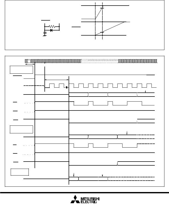
Reset
There are two kinds of resets; hardware and software. In both cases, operation is the same after the reset. (See “Software Reset” for details of software resets.) This section explains on hardware resets.
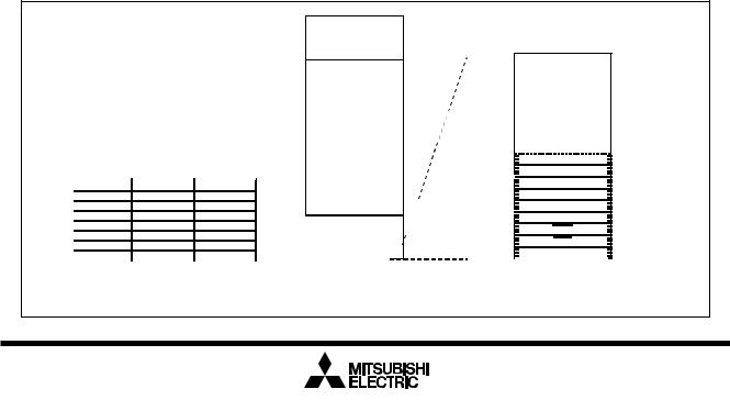
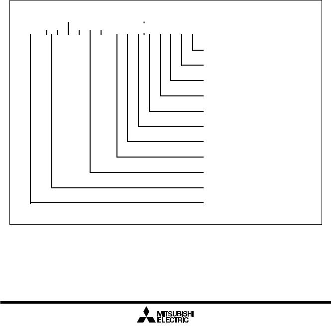
When the supply voltage is in the range where operation is guaranteed, a reset is effected by holding the reset pin level “L” (0.2VCC max.) for at least 20 cycles. When the reset pin level is then returned to the “H” level while main clock is stable, the reset status is cancelled and program execution resumes from the address in the reset vector table.
Figure 1.6.1 shows the example reset circuit. Figure 1.6.2 shows the reset sequence.
|
|
5V |
|
|
4.0V |
|
|
VCC |
|
|
0V |
RESET |
VCC |
5V |
RESET
0.8V
0V
Example when VCC = 5V.
Figure 1.6.1. Example reset circuit
XIN |
|
|
|
|
|
More than 20 cycles are needed |
|
|
|
Microprocessor |
|
|
|
|
mode BYTE = “H” |
|
|
|
|
RESET |
BCLK |
24cycles |
|
|
|
|
|
||
BCLK |
|
|
|
|
|
|
|
|
Content of reset vector |
Address |
|
FFFFC16 |
FFFFD16 |
FFFFE16 |
RD |
|
|
|
|
WR |
|
|
|
|
CS0 |
|
|
|
|
Microprocessor |
|
|
|
Content of reset vector |
mode BYTE = “L” |
|
|
|
|
Address |
|
FFFFC16 |
FFFFE16 |
|
RD |
|
|
|
|
WR |
|
|
|
|
CS0 |
|
|
|
|
Single chip |
|
FFFFC16 |
Content of reset vector |
|
mode |
|
|||
|
|
|
|
|
Address |
|
FFFFE16 |
|
|
Figure 1.6.2. Reset sequence
14
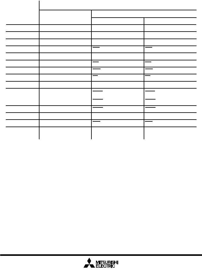
|
Mitsubishi microcomputers |
Reset |
M16C / 61 Group |
SINGLE-CHIP 16-BIT CMOS MICROCOMPUTER |
|
|
|
|
|
____________
Table 1.6.1 shows the statuses of the other pins while the RESET pin level is “L”. Figure 1.6.3 shows the
internal status of the microcomputer immediately after the reset is cancelled.
____________
Table 1.6.1. Pin status when RESET pin level is “L”
|
|
Status |
|
|
Pin name |
CNVSS = VSS |
CNVSS = VCC |
||
|
BYTE = VSS |
BYTE = VCC |
||
|
|
|||
P0 |
Input port (floating) |
Data input (floating) |
Data input (floating) |
|
|
Input port (floating) |
Data input (floating) |
|
|
P1 |
Input port (floating) |
|||
P2, P3, P40 to P43 |
Input port (floating) |
Address output (undefined) |
Address output (undefined) |
|
P44 |
Input port (floating) |
CS0 output (“H” level is output) CS0 output (“H” level is output) |
||
P45 to P47 |
Input port (floating) |
Input port (floating) |
Input port (floating) |
|
|
Input port (floating) |
|
|
|
P50 |
WR output (“H” level is output) |
WR output (“H” level is output) |
||
P51 |
Input port (floating) |
BHE output (undefined) |
BHE output (undefined) |
|
|
Input port (floating) |
|
|
|
P52 |
RD output (“H” level is output) |
RD output (“H” level is output) |
||
P53 |
Input port (floating) |
BCLK output |
BCLK output |
|
P54 |
Input port (floating) |
HLDA output (The output value |
HLDA output (The output value |
|
depends on the input to the |
depends on the input to the |
|||
|
|
|||
|
|
HOLD pin) |
HOLD pin) |
|
P55 |
Input port (floating) |
HOLD input (floating) |
HOLD input (floating) |
|
|
Input port (floating) |
ALE output (“L” level is output) |
|
|
P56 |
ALE output (“L” level is output) |
|||
P57 |
Input port (floating) |
RDY input (floating) |
RDY input (floating) |
|
P6, P7, P80 to P84, |
Input port (floating) |
Input port (floating) |
Input port (floating) |
|
P86, P87, P9, P10 |
||||
|
|
|
||
|
|
|
|
|
15
|
Mitsubishi microcomputers |
Reset |
M16C / 61 Group |
SINGLE-CHIP 16-BIT CMOS MICROCOMPUTER |
|
|
|
|
|
(1) Processor mode register 0 (Note) |
(000416)··· |
|
|
|
0016 |
|
|
|
|
(2) Processor mode register 1 |
(000516)··· |
|
|
|
|
|
|
|
|
0 |
0 |
|
|
|
|
|
0 |
||
(3) System clock control register 0 |
(000616)··· |
|
|
|
|
|
|
|
|
0 |
1 |
0 |
0 |
1 |
0 |
0 |
0 |
||
(4) System clock control register 1 |
(000716)··· |
|
|
|
|
|
|
|
|
0 |
0 |
1 |
0 |
0 |
0 |
0 |
0 |
||
(5) Chip select control register |
(000816)··· |
|
|
|
|
|
|
|
|
0 |
0 |
0 |
0 |
0 |
0 |
0 |
1 |
||
(6) Address match interrupt enable register |
(000916)··· |
|
|
|
|
|
|
|
|
|
|
|
|
|
|
0 |
0 |
||
(7) Protect register |
(000A16)··· |
|
|
|
|
|
|
|
|
|
|
|
|
|
0 |
0 |
0 |
||
(8) Watchdog timer control register |
(000F16)··· |
|
|
|
|
||||
0 |
0 |
0 |
? |
? |
? |
? |
? |
||
(9) Address match interrupt register 0 |
(001016)··· |
|
|
|
|
|
|
|
|
|
|
|
0016 |
|
|
|
|||
|
(001116)··· |
|
|
|
|
|
|
|
|
|
|
|
|
|
|
|
|
||
|
|
|
|
0016 |
|
|
|
||
|
(001216)··· |
|
|
|
|
|
|
|
|
|
|
|
|
|
|
|
|
|
|
|
|
|
|
|
0 |
0 |
0 |
0 |
|
(10) Address match interrupt register 1 |
(001416)··· |
|
|
|
|
|
|
|
|
|
|
|
0016 |
|
|
|
|||
|
(001516)··· |
|
|
|
|
|
|
|
|
|
|
|
|
0016 |
|
|
|
||
|
(001616)··· |
|
|
|
|
|
|
|
|
|
|
|
|
|
|
|
|
|
|
|
|
|
|
|
0 |
0 |
0 |
0 |
|
(11)DMA0 control register |
(002C16)··· |
|
|
|
|
|
|
|
|
0 |
0 |
0 |
0 |
0 |
? |
0 |
0 |
||
(12)DMA1 control register |
(003C16)··· |
|
|
|
|
|
|
|
|
0 |
0 |
0 |
0 |
0 |
? |
0 |
0 |
||
Bus collision detection interrupt control |
|
|
|
|
|
|
|
|
|
(13)register |
(004A16)··· |
|
|
|
|
? |
0 |
0 |
0 |
|
|
|
|
|
|
|
|
|
|
(14) DMA0 interrupt control register |
(004B16)··· |
|
|
|
|
? |
0 |
0 |
0 |
(15) DMA1 interrupt control register |
(004C16)··· |
|
|
|
|
|
|
|
|
|
|
|
|
|
|
|
|
||
|
|
|
|
? |
0 |
0 |
0 |
||
(16) Key input interrupt control register |
(004D16)··· |
|
|
|
|
|
|
|
|
|
|
|
|
? |
0 |
0 |
0 |
||
(17) A-D conversion interrupt control register |
(004E16)··· |
|
|
|
|
|
|
|
|
|
|
|
|
? |
0 |
0 |
0 |
||
(18)UART2 transmit interrupt control register |
(004F16)··· |
|
|
|
|
|
|
|
|
|
|
|
|
|
|
|
|
||
|
|
|
|
? |
0 |
0 |
0 |
||
(19)UART2 receive interrupt control register |
(005016)··· |
|
|
|
|
|
|
|
|
|
|
|
|
|
|
|
|
||
|
|
|
|
? |
0 |
0 |
0 |
||
(20)UART0 transmit interrupt control register |
(005116)··· |
|
|
|
|
|
|
|
|
|
|
|
|
? |
0 |
0 |
0 |
||
(21)UART0 receive interrupt control register |
(005216)··· |
|
|
|
|
|
|
|
|
|
|
|
|
? |
0 |
0 |
0 |
||
(22)UART1 transmit interrupt control register |
(005316)··· |
|
|
|
|
|
|
|
|
|
|
|
|
? |
0 |
0 |
0 |
||
(23)UART1 receive interrupt control register |
(005416)··· |
|
|
|
|
|
|
|
|
|
|
|
|
|
|
|
|
||
|
|
|
|
? |
0 |
0 |
0 |
||
(24)Timer A0 interrupt control register |
(005516)··· |
|
|
|
|
|
|
|
|
|
|
|
|
|
|
|
|
||
|
|
|
|
? |
0 |
0 |
0 |
||
(25)Timer A1 interrupt control register |
(005616)··· |
|
|
|
|
|
|
|
|
|
|
|
|
? |
0 |
0 |
0 |
||
(26)Timer A2 interrupt control register |
(005716)··· |
|
|
|
|
|
|
|
|
|
|
|
|
? |
0 |
0 |
0 |
||
(27)Timer A3 interrupt control register |
(005816)··· |
|
|
|
|
|
|
|
|
|
|
|
|
|
|
|
|
||
|
|
|
|
? |
0 |
0 |
0 |
||
(28)Timer A4 interrupt control register |
(005916)··· |
|
|
|
|
|
|
|
|
|
|
|
|
|
|
|
|
||
|
|
|
|
? |
0 |
0 |
0 |
||
(29)Timer B0 interrupt control register |
(005A16)··· |
|
|
|
|
|
|
|
|
|
|
|
|
? |
0 |
0 |
0 |
||
(30)Timer B1 interrupt control register |
(005B16)··· |
|
|
|
|
|
|
|
|
|
|
|
|
? |
0 |
0 |
0 |
||
(31)Timer B2 interrupt control register |
(005C16)··· |
|
|
|
|
|
|
|
|
|
|
|
|
? |
0 |
0 |
0 |
||
(32) INT0 interrupt control register |
(005D16)··· |
|
|
|
|
|
|
|
|
|
|
|
|
|
|
||||
|
|
0 |
0 |
? |
0 |
0 |
0 |
||
(33) INT1 interrupt control register |
(005E16)··· |
|
|
|
|
|
|
||
|
|
0 |
0 |
? |
0 |
0 |
0 |
||
(34) INT2 interrupt control register |
(005F16)··· |
|
|
|
|
|
|
||
|
|
0 |
0 |
? |
0 |
0 |
0 |
||
(35)UART2 transmit/receive mode register |
(037816)··· |
|
|
|
|
|
|
|
|
|
|
|
|
|
|
|
|||
|
|
|
0016 |
|
|
|
|||
(36)UART2 transmit/receive control register 0 |
(037C16)··· |
|
|
|
|
|
|
|
|
|
|
|
|
|
|
|
|
||
0 |
0 |
0 |
0 |
1 |
0 |
0 |
0 |
||
(37)UART2 transmit/receive control register 1 |
(037D16)··· |
|
|
|
|
|
|
|
|
0 |
0 |
0 |
0 |
0 |
0 |
1 |
0 |
||
(38)Count start flag |
(038016)··· |
|
|
|
|
|
|
|
|
|
|
|
0016 |
|
|
|
|||
(39) Clock prescaler reset flag |
(038116)··· |
|
|
|
|
|
|
|
|
0 |
|
|
|
|
|
|
|
||
(40)One-shot start flag |
(038216)··· |
|
|
|
|
|
|
|
|
|
|
|
|
|
|
|
|
||
0 |
0 |
|
0 |
0 |
0 |
0 |
0 |
||
(41)Trigger select flag |
(038316)··· |
|
|
|
|
|
|
|
|
|
|
|
|
|
|
|
|||
|
|
|
0016 |
|
|
|
|||
(42) Up-down flag |
(038416)··· |
|
|
|
|
|
|
|
|
|
|
|
0016 |
|
|
|
|||
(43) Timer A0 mode register |
(039616)··· |
|
|
|
|
0016 |
|
|
|
|
(44) Timer A1 mode register |
(039716)··· |
|
|
|
|
|
|
|
|
|
|
|
|
|
0016 |
|
|
|
|||
(45) Timer A2 mode register |
(039816)··· |
|
|
|
|
|
|
|
|
|
|
|
|
|
0016 |
|
|
|
|||
(46) Timer A3 mode register |
(039916)··· |
|
|
|
|
|
|
|
|
|
|
|
|
|
0016 |
|
|
|
|||
|
|
|
|
|
|
|
|
|
|
|
|
|
|
|
|
|
|
|
|
|
|
(47) Timer A4 mode register |
(039A16)··· |
|
|
|
0016 |
|
|
|
||
(48) Timer B0 mode register |
(039B16)··· |
|
|
|
|
|
|
|
|
|
|
|
|
|
|
|
|
|
|||
0 |
0 |
? |
|
0 |
0 |
0 |
0 |
|||
|
|
|
|
|
|
|
|
|
|
|
(49) Timer B1 mode register |
(039C16)··· |
0 |
0 |
? |
|
0 |
0 |
0 |
0 |
|
|
|
|
|
|
|
|
|
|
|
|
(50) Timer B2 mode register |
(039D16)··· |
0 |
0 |
? |
|
0 |
0 |
0 |
0 |
|
|
|
|
|
|
|
|
|
|
|
|
(51) UART0 transmit/receive mode register |
(03A016)··· |
|
|
|
0016 |
|
|
|
||
|
|
|
|
|
|
|
|
|
|
|
|
|
|
|
|
|
|
|
|
|
|
(52) UART0 transmit/receive control register 0 |
(03A416)··· |
0 |
0 |
0 |
0 |
1 |
0 |
0 |
0 |
|
|
|
|
|
|
|
|
|
|
|
|
|
|
|
|
|
|
|
|
|
|
|
(53) UART0 transmit/receive control register 1 |
(03A516)··· |
0 |
0 |
0 |
0 |
0 |
0 |
1 |
0 |
|
|
|
|
|
|
|
|
|
|
|
|
(54) UART1 transmit/receive mode register |
(03A816)··· |
|
|
|
0016 |
|
|
|
||
|
|
|
|
|
|
|
|
|
|
|
(55) UART1 transmit/receive control register 0 |
(03AC16)··· |
0 |
0 |
0 |
0 |
1 |
0 |
0 |
0 |
|
|
|
|
|
|
|
|
|
|
|
|
|
|
|
|
|
|
|
|
|
|
|
(56) UART1 transmit/receive control register 1 |
(03AD16)··· |
0 |
0 |
0 |
0 |
0 |
0 |
1 |
0 |
|
(57) UART transmit/receive control register 2 |
(03B016)··· |
|
|
|
|
|
|
|
|
|
|
0 |
0 |
0 |
0 |
0 |
0 |
0 |
|||
|
|
|
|
|
|
|
|
|
|
|
(58) DMA0 cause select register |
(03B816)··· |
|
|
|
0016 |
|
|
|
||
|
|
|
|
|
|
|
|
|
|
|
(59) DMA1 cause select register |
(03BA16)··· |
|
|
|
0016 |
|
|
|
||
(60) A-D control register 2 |
(03D416)··· |
|
|
|
|
|
|
|
|
|
|
|
|
|
|
|
|
|
|||
0 |
0 |
0 |
0 |
|
|
|
0 |
|||
|
|
|
|
|
|
|
|
|
|
|
|
|
|
|
|
|
|
|
|
|
|
(61) A-D control register 0 |
(03D616)··· |
0 |
0 |
0 |
0 |
0 |
? |
? |
? |
|
|
|
|
|
|
|
|
|
|
|
|
(62) A-D control register 1 |
(03D716)··· |
|
|
|
0016 |
|
|
|
||
|
|
|
|
|
|
|
|
|
|
|
(63)D-A control register |
(03DC16)··· |
|
|
|
0016 |
|
|
|
||
|
|
|
|
|
|
|
|
|
|
|
(64)Port P0 direction register |
(03E216)··· |
|
|
|
0016 |
|
|
|
||
(65)Port P1 direction register |
|
|
|
|
|
|
|
|
|
|
|
|
|
|
|
|
|
|
|
|
|
(03E316)··· |
|
|
|
0016 |
|
|
|
|||
(66)Port P2 direction register |
|
|
|
|
|
|
|
|
|
|
(03E616)··· |
|
|
|
0016 |
|
|
|
|||
(67)Port P3 direction register |
|
|
|
|
|
|
|
|
|
|
(03E716)··· |
|
|
|
0016 |
|
|
|
|||
(68)Port P4 direction register |
|
|
|
|
|
|
|
|
|
|
(03EA16)··· |
|
|
|
0016 |
|
|
|
|||
(69)Port P5 direction register |
|
|
|
|
|
|
|
|
|
|
(03EB16)··· |
|
|
|
0016 |
|
|
|
|||
(70)Port P6 direction register |
|
|
|
|
|
|
|
|
|
|
(03EE16)··· |
|
|
|
0016 |
|
|
|
|||
(71)Port P7 direction register |
|
|
|
|
|
|
|
|
|
|
(03EF16)··· |
|
|
|
0016 |
|
|
|
|||
(72)Port P8 direction register |
|
|
|
|
|
|
|
|
|
|
(03F216)··· |
|
0 |
0 |
|
0 |
0 |
0 |
0 |
0 |
|
(73)Port P9 direction register |
(03F316)··· |
|
|
|
|
|
|
|
|
|
|
|
|
0016 |
|
|
|
||||
(74) Port P10 direction register |
|
|
|
|
|
|
|
|
|
|
|
|
|
|
|
|
|
|
|
|
|
(03F616)··· |
|
|
|
0016 |
|
|
|
|||
(75) Pull-up control register 0 |
|
|
|
|
|
|
|
|
|
|
(03FC16)··· |
|
|
|
0016 |
|
|
|
|||
(76) Pull-up control register 1 |
|
|
|
|
|
|
|
|
|
|
(03FD16)··· |
|
|
|
0016 |
|
|
|
|||
(77) Pull-up control register 2 |
|
|
|
|
|
|
|
|
|
|
(03FE16)··· |
|
|
|
0016 |
|
|
|
|||
(78) Data registers (R0/R1/R2/R3) |
|
|
|
|
|
|
|
|
|
|
|
|
|
|
|
|
|
|
|
|
|
|
|
|
|
000016 |
|
|
||||
(79) Address registers (A0/A1) |
|
|
|
|
|
|
|
|
|
|
|
|
|
|
000016 |
|
|
||||
(80) Frame base register (FB) |
|
|
|
|
|
|
|
|
|
|
|
|
|
|
000016 |
|
|
||||
(81) Interrupt table register (INTB) |
|
|
|
|
|
|
|
|
|
|
|
|
|
|
|
|
|
|
|
|
|
|
|
|
|
0000016 |
|
|
||||
(82) User stack pointer (USP) |
|
|
|
|
|
|
|
|
|
|
|
|
|
|
000016 |
|
|
||||
(83) Interrupt stack pointer (ISP) |
|
|
|
|
|
|
|
|
|
|
|
|
|
|
000016 |
|
|
||||
(84) Static base register (SB) |
|
|
|
|
|
|
|
|
|
|
|
|
|
|
000016 |
|
|
||||
(85) Flag register (FLG) |
|
|
|
|
|
|
|
|
|
|
|
|
|
|
000016 |
|
|
||||
x : Nothing is mapped to this bit |
|
|
|
|
|
|
|
|
|
|
|
|
|
|
|
|
|
|
|
|
|
? : Undefined |
|
|
|
|
|
|
|
|
|
|
The content of other registers and RAM is undefined when the microcomputer is reset. The initial values must therefore be set.
Note: When the VCC level is applied to the CNVSS pin, it is 0316 at a reset.
Figure 1.6.3. Device's internal status after a reset is cleared
16
|
Mitsubishi microcomputers |
SFR |
M16C / 61 Group |
SINGLE-CHIP 16-BIT CMOS MICROCOMPUTER |
|
|
|
|
|
000016
000116
000216
000316
000416
000516
000616
000716
000816
000916
000A16
000B16
000C16
000D16
000E16
000F16
001016
001116
001216
001316
001416
001516
001616
001716
001816
001916
001A16
001B16
001C16
001D16
001E16
001F16
002016
002116
002216
002316
002416
002516
002616
002716
002816
002916
002A16
002B16
002C16
002D16
002E16
002F16
003016
003116
003216
003316
003416
003516
003616
003716
003816
003916
003A16
003B16
003C16
003D16
003E16
003F16
Processor mode register 0 (PM0) Processor mode register 1(PM1) System clock control register 0 (CM0) System clock control register 1 (CM1) Chip select control register (CSR)
Address match interrupt enable register (AIER) Protect register (PRCR)
Watchdog timer start register (WDTS) Watchdog timer control register (WDC)
Address match interrupt register 0 (RMAD0)
Address match interrupt register 1 (RMAD1)
DMA0 source pointer (SAR0)
DMA0 destination pointer (DAR0)
DMA0 transfer counter (TCR0)
DMA0 control register (DM0CON)
DMA1 source pointer (SAR1)
DMA1 destination pointer (DAR1)
DMA1 transfer counter (TCR1)
DMA1 control register (DM1CON)
004016 |
|
|
004116 |
|
|
004216 |
|
|
004316 |
|
|
004416 |
|
|
004516 |
|
|
004616 |
|
|
004716 |
|
|
004816 |
|
|
004916 |
|
|
004A16 |
Bus collision detection interrupt control register (BCNIC) |
|
004B16 |
DMA0 interrupt control register (DM0IC) |
|
004C16 |
DMA1 interrupt control register (DM1IC) |
|
004D16 |
Key input interrupt control register (KUPIC) |
|
004E16 |
A-D conversion interrupt control register (ADIC) |
|
004F16 |
UART2 transmit interrupt control register (S2TIC) |
|
005016 |
UART2 receive interrupt control register (S2RIC) |
|
005116 |
UART0 transmit interrupt control register (S0TIC) |
|
005216 |
UART0 receive interrupt control register (S0RIC) |
|
005316 |
UART1 transmit interrupt control register (S1TIC) |
|
005416 |
UART1 receive interrupt control register (S1RIC) |
|
005516 |
Timer A0 interrupt control register (TA0IC) |
|
005616 |
Timer A1 interrupt control register (TA1IC) |
|
005716 |
Timer A2 interrupt control register (TA2IC) |
|
005816 |
Timer A3 interrupt control register (TA3IC) |
|
005916 |
Timer A4 interrupt control register (TA4IC) |
|
005A16 |
Timer B0 interrupt control register (TB0IC) |
|
005B16 |
Timer B1 interrupt control register (TB1IC) |
|
005C16 |
Timer B2 interrupt control register (TB2IC) |
|
005D16 |
INT0 interrupt control register (INT0IC) |
|
005E16 |
INT1 interrupt control register (INT1IC) |
|
005F16 |
INT2 interrupt control register (INT2IC) |
|
036316 |
|
|
|
||
|
||
|
||
036416 |
|
|
036516 |
|
|
036616 |
|
|
036716 |
|
|
036816 |
|
|
036916 |
|
|
036A16 |
|
|
|
||
036B16 |
|
|
|
||
036C16 |
|
|
036D16 |
|
|
|
||
036E16 |
|
|
036F16 |
|
|
|
||
037016 |
|
|
037116 |
|
|
|
||
037216 |
|
|
|
||
037316 |
|
|
|
||
037416 |
|
|
|
||
037516 |
|
|
|
||
037616 |
|
|
|
||
037716 |
|
|
|
||
037816 |
UART2 transmit/receive mode register (U2MR) |
|
037916 |
||
UART2 bit rate generator (U2BRG) |
||
037A16 |
||
UART2 transmit buffer register (U2TB) |
||
037B16 |
||
037C16 |
UART2 transmit/receive control register 0 (U2C0) |
|
037D16 |
UART2 transmit/receive control register 1 (U2C1) |
|
037E16 |
UART2 receive buffer register (U2RB) |
|
037F16 |
||
|
||
|
|
Figure 1.7.1. Location of peripheral unit control registers
17

|
Mitsubishi microcomputers |
SFR |
M16C / 61 Group |
SINGLE-CHIP 16-BIT CMOS MICROCOMPUTER |
|
|
|
|
|
038016
038116
038216
038316
038416
038516
038616
038716
038816
038916
038A16
038B16
038C16
038D16
038E16
038F16
039016
039116
039216
039316
039416
039516
039616
039716
039816
039916
039A16
039B16
039C16
039D16
039E16
039F16
03A016
03A116
03A216
03A316
03A416
03A516
03A616
03A716
03A816
03A916
03AA16
03AB16
03AC16
03AD16
03AE16
03AF16
03B016
03B116
03B216
03B316
03B416
03B516
03B616
03B716
03B816
03B916
03BA16
03BB16
03BC16
03BD16
03BE16
03BF16
Count start flag (TABSR)
Clock prescaler reset flag (CPSRF) One-shot start flag (ONSF)
Trigger select register (TRGSR) Up-down flag (UDF)
Timer A0 (TA0)
Timer A1 (TA1)
Timer A2 (TA2)
Timer A3 (TA3)
Timer A4 (TA4)
Timer B0 (TB0)
Timer B1 (TB1)
Timer B2 (TB2)
Timer A0 mode register (TA0MR)
Timer A1 mode register (TA1MR)
Timer A2 mode register (TA2MR)
Timer A3 mode register (TA3MR)
Timer A4 mode register (TA4MR)
Timer B0 mode register (TB0MR)
Timer B1 mode register (TB1MR)
Timer B2 mode register (TB2MR)
UART0 transmit/receive mode register (U0MR)
UART0 bit rate generator (U0BRG)
UART0 transmit buffer register (U0TB)
UART0 transmit/receive control register 0 (U0C0) UART0 transmit/receive control register 1 (U0C1)
UART0 receive buffer register (U0RB)
UART1 transmit/receive mode register (U1MR)
UART1 bit rate generator (U1BRG)
UART1 transmit buffer register (U1TB)
UART1 transmit/receive control register 0 (U1C0) UART1 transmit/receive control register 1 (U1C1)
UART1 receive buffer register (U1RB)
UART transmit/receive control register 2 (UCON)
DMA0 cause select register (DM0SL)
DMA1 cause select register (DM1SL)
CRC data register (CRCD)
CRC input register (CRCIN)
03C016
03C116
03C216
03C316
03C416
03C516
03C616
03C716
03C816
03C916
03CA16
03CB16
03CC16
03CD16
03CE16
03CF16
03D016
03D116
03D216
03D316
03D416
03D516
03D616
03D716
03D816
03D916
03DA16
03DB16
03DC16
03DD16
03DE16
03DF16
03E016
03E116
03E216
03E316
03E416
03E516
03E616
03E716
03E816
03E916
03EA16
03EB16
03EC16
03ED16
03EE16
03EF16
03F016
03F116
03F216
03F316
03F416
03F516
03F616
03F716
03F816
03F916
03FA16
03FB16
03FC16
03FD16
03FE16
03FF16
A-D register 0 (AD0)
A-D register 1 (AD1)
A-D register 2 (AD2)
A-D register 3 (AD3)
A-D register 4 (AD4)
A-D register 5 (AD5)
A-D register 6 (AD6)
A-D register 7 (AD7)
A-D control register 2 (ADCON2)
A-D control register 0 (ADCON0) A-D control register 1 (ADCON1) D-A register 0 (DA0)
D-A register 1 (DA1)
D-A control register (DACON)
Port P0 (P0)
Port P1 (P1)
Port P0 direction register (PD0) Port P1 direction register (PD1) Port P2 (P2)
Port P3 (P3)
Port P2 direction register (PD2) Port P3 direction register (PD3) Port P4 (P4)
Port P5 (P5)
Port P4 direction register (PD4) Port P5 direction register (PD5) Port P6 (P6)
Port P7 (P7)
Port P6 direction register (PD6) Port P7 direction register (PD7) Port P8 (P8)
Port P9 (P9)
Port P8 direction register (PD8) Port P9 direction register (PD9) Port P10 (P10)
Port P10 direction register (PD10)
Pull-up control register 0 (PUR0) Pull-up control register 1 (PUR1) Pull-up control register 2 (PUR2)
Figure 1.7.2. Location of peripheral unit control registers
18

|
Mitsubishi microcomputers |
Software Reset |
M16C / 61 Group |
SINGLE-CHIP 16-BIT CMOS MICROCOMPUTER |
|
|
|
|
|
Software Reset
Writing “1” to bit 3 of the processor mode register 0 (address 000416) applies a (software) reset to the microcomputer. A software reset has almost the same effect as a hardware reset. The contents of internal RAM are preserved.
Processor Mode
(1) Types of Processor Mode
One of three processor modes can be selected: single-chip mode, memory expansion mode, and microprocessor mode. The functions of some pins, the memory map, and the access space differ according to the selected processor mode.
•Single-chip mode
In single-chip mode, only internal memory space (SFR, internal RAM, and internal ROM) can be accessed. Ports P0 to P10 can be used as programmable I/O ports or as I/O ports for the internal peripheral functions.
•Memory expansion mode
In memory expansion mode, external memory can be accessed in addition to the internal memory space (SFR, internal RAM, and internal ROM).
In this mode, some of the pins function as the address bus, the data bus, and as control signals. The number of pins assigned to these functions depends on the bus and register settings. (See “Bus Settings” for details.)
•Microprocessor mode
In microprocessor mode, the SFR, internal RAM, and external memory space can be accessed. The internal ROM area cannot be accessed.
In this mode, some of the pins function as the address bus, the data bus, and as control signals. The number of pins assigned to these functions depends on the bus and register settings. (See “Bus Settings” for details.)
(2)Setting Processor Modes
The processor mode is set using the CNVSS pin and the processor mode bits (bits 1 and 0 at address 000416). Do not set the processor mode bits to “102”.
Regardless of the level of the CNVSS pin, changing the processor mode bits selects the mode. Therefore, never change the processor mode bits when changing the contents of other bits. Also do not attempt to shift to or from the microprocessor mode within the program stored in the internal ROM area.
•Applying VSS to CNVSS pin
The microcomputer begins operation in single-chip mode after being reset. Memory expansion mode is selected by writing “012” to the processor mode is selected bits.
•Applying VCC to CNVSS pin
The microcomputer starts to operate in microprocessor mode after being reset.
Figure 1.8.1 shows the processor mode register 0 and 1. Figure 1.9.1 shows the memory maps appli-
cable for each of the modes.
19
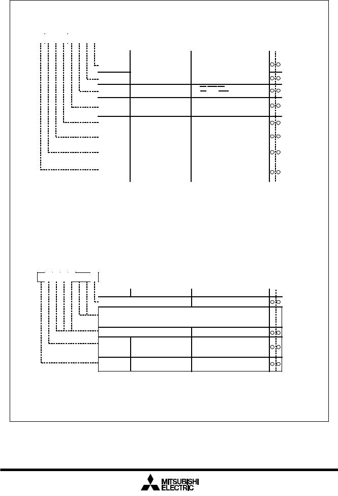
|
Mitsubishi microcomputers |
Processor Mode |
M16C / 61 Group |
SINGLE-CHIP 16-BIT CMOS MICROCOMPUTER |
|
|
|
|
|
Processor mode register 0 (Note 1)
b7 |
b6 |
b5 |
b4 |
b3 |
b2 |
b1 |
b0 |
Symbol |
Address |
When reset |
|
PM0 |
000416 |
0016 (Note 2) |
|||||||||
|
|
|
|
|
|
|
|
||||
|
|
|
|
|
|
|
|
|
|
|
Bit symbol |
Bit name |
|
Function |
R W |
PM00 |
Processor mode bit |
b1 b0 |
|
|
|
||||
0 |
0: Single-chip mode |
|
||
|
|
|
||
|
|
0 |
1: Memory expansion mode |
|
PM01 |
|
1 |
0: Inhibited |
|
|
1 |
1: Microprocessor mode |
|
|
|
|
|
||
PM02 |
R/W mode select bit |
0 |
: RD,BHE,WR |
|
|
|
1 |
: RD,WRH,WRL |
|
PM03 |
Software reset bit |
The device is reset when this bit is set |
|
|
|
|
to “1”. The value of this bit is “0” when |
||
|
|
read. |
|
|
|
Multiplexed bus space |
b5 b4 |
|
|
PM04 |
|
|||
0 0 : Multiplexed bus is not used |
|
|||
|
select bit |
|
||
|
0 1 : Allocated to CS2 space |
|
||
|
|
|
||
PM05 |
|
1 0 : Allocated to CS1 space |
|
|
|
1 1 : Allocated to entire space (Note4) |
|
||
|
|
|
||
|
|
|
|
|
PM06 |
Port P40 to P43 function |
0 : Address output |
|
|
|
select bit (Note 3) |
1 : Port function |
|
|
|
|
|
(Address is not output) |
|
PM07 |
BCLK output disable bit |
0 : BCLK is output |
|
|
|
|
1 : BCLK is not output |
|
|
|
|
|
(Pin is left floating) |
|
|
|
|
|
|
Note 1: Set bit 1 of the protect register (address 000A16) to “1” when writing new values to this register.
Note 2: If the VCC voltage is applied to the CNVSS, the value of this register when reset is 0316. (PM00 and PM01 both are set to “1”.)
Note 3: Valid in microprocessor and memory expansion modes.
Note 4: If the entire space is of multiplexed bus in memory expansion mode, choose an 8-bit width.The processor operates using the separate bus after reset is
revoked, so the entire space multiplexed bus cannot be chosen in microprocessor mode.
The higher-order address becomes a port if the entire space multiplexed bus is chosen, so only 256 bytes can be used in each chip select.
Processor mode register 1 (Note 1)
b7 b6 b5 b4 b3 b2 b1 b0
0 0 0 
 0
0
Symbol |
Address |
When reset |
PM1 |
000516 |
00XXXXX02 |
Bit symbol |
Bit name |
Function |
R W |
Reserved bit |
|
Must always be set to “0” |
|
|
|
||
|
|
||
|
|
|
|
Nothing is assigned.
In an attempt to write to these bits, write “0”. The value, if read, turns out to be
 indeterminate.
Reserved bit |
|
Must always be set to “0” |
|
PM16 |
External memory area |
0 : Do not expand |
|
|
expansion bit (Note 2) |
||
|
1 : Expand |
||
|
|
||
PM17 |
Wait bit |
0 |
: No wait state |
|
|
1 |
: Wait state |
Note 1: Set bit 1 of the protect register (address 000A16) to “1” when writing new values to this register.
Note 2: When this bit is set to “1” in memory expansion mode, M30612M4A/E4 provides the means of using part of internal reserved area as an external area. Set this bit to “0” except M30612M4A/E4. Set this bit to “0” in single chip mode.
Figure 1.8.1. Processor mode register 0 and 1
20
|
Mitsubishi microcomputers |
Processor Mode |
M16C / 61 Group |
SINGLE-CHIP 16-BIT CMOS MICROCOMPUTER |
|
|
|
|
|
Single-chip mode |
Memory expansion mode |
Microprocessor mode |
||||||||||||
0000016 |
|
|
|
|
|
|
|
|
|
|
|
|
|
|
SFR area |
|
|
|
SFR area |
|
|
|
|
SFR area |
|
||||
|
|
|
|
|
|
|
|
|
||||||
0040016 |
Internal RAM |
|
|
|
Internal RAM |
|
|
|
|
Internal RAM |
|
|||
|
|
|
|
|
|
|
|
|||||||
|
|
|
|
|
|
|
|
|
||||||
|
area |
|
|
|
area |
|
|
|
|
area |
|
|||
XXXXX16 |
|
|
|
|
|
|
|
|
|
|
|
|
|
|
|
|
|
|
|
|
Internally |
|
|
|
|
Internally |
|
||
|
|
|
|
|
|
reserved area |
|
|
|
|
reserved area |
|
||
0400016 |
|
|
|
|
|
|
|
|
|
|
|
|
|
|
|
|
|
|
|
|
|
|
|
|
|
|
|
|
|
|
|
|
|
|
|
|
|
|
|
|
|
|
||
|
Inhibited |
|
|
|
External area |
|
|
|
|
|
|
|
|
|
D000016 |
|
|
|
|
|
|
|
|
|
|
|
|
|
|
|
|
|
|
Internally reserved |
|
|
|
|
External area |
|
|
|||
|
|
|
|
|
|
|
|
|
|
|
||||
YYYYY16 |
|
|
|
|
|
area (Note 1) |
|
|
|
|
|
|
|
|
Internal ROM |
|
|
|
Internal ROM |
|
|
|
|
|
|
|
|||
|
|
|
|
|
|
|
|
|
|
|||||
|
|
|
|
|
|
|
|
|
|
|
||||
FFFFF16 |
area (Note 2) |
|
|
|
area |
|
|
|
|
|
|
|
||
|
|
|
|
|
|
|
|
|
|
|
|
|
|
|
Type No. |
Address |
Address |
|
XXXXX16 |
YYYYY16 |
||
|
|||
M30610M8A |
02BFF16 |
F000016 |
|
M30610MAA |
02BFF16 |
E800016 |
|
M30610MCA/EC |
02BFF16 |
E000016 |
|
M30612M4A/E4 |
013FF16 |
F800016 |
|
M30612M8A |
013FF16 |
F000016 |
|
M30612MAA |
013FF16 |
E800016 |
|
M30612MCA |
017FF16 |
E000016 |
|
External area : Accessing this area allows the user to access a device connected externally to the microcomputer.
Note 1: This area becomes external area when PM16 (external memory area expansion bit ) = “1” in M30612M4A/E4. Set “0” except M30612M4A/E4.
Note 2: Set “0” to PM16 (external memory area expansion bit) in single chip mode. 

Figure 1.9.1. Memory maps in each processor mode
21

|
Mitsubishi microcomputers |
Bus Settings |
M16C / 61 Group |
SINGLE-CHIP 16-BIT CMOS MICROCOMPUTER |
|
|
|
|
|
Bus Settings
The BYTE pin and bits 4 to 6 of the processor mode register 0 (address 000416) are used to change the bus settings.
Table 1.10.1 shows the factors used to change the bus settings.
Table 1.10.1. Factors for switching bus settings
Bus setting |
Switching factor |
|
|
Switching external address bus width |
Bit 6 of processor mode register 0 |
|
|
Switching external data bus width |
BYTE pin |
|
|
Switching between separate and multiplex bus |
Bits 4 and 5 of processor mode register 0 |
|
|
(1) Selecting external address bus width
The address bus width for external output in the 1M bytes of address space can be set to 16 bits (64K bytes address space) or 20 bits (1M bytes address space). When bit 6 of the processor mode register 0 is set to “1”, the external address bus width is set to 16 bits, and P2 and P3 become part of the address bus. P40 to P43 can be used as programmable I/O ports. When bit 6 of processor mode register 0 is set to “0”, the external address bus width is set to 20 bits, and P2, P3, and P40 to P43 become part of the address bus.
(2) Selecting external data bus width
The external data bus width can be set to 8 or 16 bits. (Note, however, that only the separate bus can be set.) When the BYTE pin is “L”, the bus width is set to 16 bits; when “H”, it is set to 8 bits. (The internal bus width is permanently set to 16 bits.) While operating, fix the BYTE pin either to “H” or to “L”.
(3) Selecting separate/multiplex bus
The bus format can be set to multiplex or separate bus using bits 4 and 5 of the processor mode register 0.
•Separate bus
In this mode, the data and address are input and output separately. The data bus can be set using the BYTE pin to be 8 or 16 bits. When the BYTE pin is “H”, the data bus is set to 8 bits and P0 functions as the data bus and P1 as a programmable I/O port. When the BYTE pin is “L”, the data bus is set to 16 bits and P0 and P1 are both used for the data bus.
When the separate bus is used for access, a software wait can be selected.
•Multiplex bus
In this mode, data and address I/O are time multiplexed. With an 8-bit data bus selected (BYTE pin = “H”), the 8 bits from D0 to D7 are multiplexed with A0 to A7.
With a 16-bit data bus selected (BYTE pin = “L”), the 8 bits from D0 to D7 are multiplexed with A1 to A8. D8 to D15 are not multiplexed. In this case, the external devices connected to the multiplexed bus are mapped to the microcomputer’s even addresses (every 2nd address). To access these external devices, access the even addresses as bytes.
The ALE signal latches the address. It is output from P56.
Before using the multiplex bus for access, be sure to insert a software wait.
If the entire space is of multiplexed bus in memory expansion mode, choose an 8-bit width.
The processor operates using the separate bus after reset is revoked, so the entire space multiplexed bus cannot be chosen in microprocessor mode.
The higher-order address becomes a port if the entire space multiplexed bus is chosen, so only 256 bytes can be used in each chip select.
22
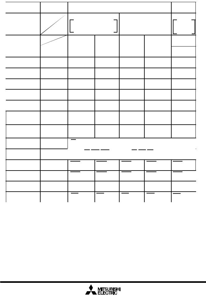
|
Mitsubishi microcomputers |
Bus Settings |
M16C / 61 Group |
SINGLE-CHIP 16-BIT CMOS MICROCOMPUTER |
|
|
|
|
|
Table 1.10.2. Pin functions for each processor mode
|
Processor mode |
Single-chip |
Memory expansion mode/microprocessor modes |
|||
|
mode |
|||||
|
|
|
|
|
|
|
|
|
|
“01”, “10” |
|
“00” |
|
|
Multiplexed bus |
|
Either CS1 or CS2 is for |
|
|
|
|
space select bit |
|
multiplexed bus and others |
(separate bus) |
||
|
|
|
are for separate bus |
|||
|
|
|
|
|
||
|
Data bus width |
|
8 bits |
16 bits |
8 bits |
16 bits |
|
BYTE pin level |
|
“H” |
“L” |
“H” |
“L” |
|
|
|
|
|
|
|
|
P00 to P07 |
I/O port |
Data bus |
Data bus |
Data bus |
Data bus |
|
P10 to P17 |
I/O port |
I/O port |
Data bus |
I/O port |
Data bus |
|
P20 |
I/O port |
Address bus |
Address bus |
Address bus |
Address bus |
|
|
|
/data bus(Note 2) |
|
|
|
|
P21 to P27 |
I/O port |
Address bus |
Address bus |
Address bus |
Address bus |
|
|
|
/data bus(Note 2) |
/data bus(Note 2) |
|
|
|
P30 |
I/O port |
Address bus |
Address bus |
Address bus |
Address bus |
|
|
|
/data bus(Note 2) |
|
|
|
|
P31 to P37 |
I/O port |
Address bus |
Address bus |
Address bus |
Address bus |
|
P40 to P43 |
I/O port |
I/O port |
I/O port |
/O port |
I/O port |
|
||||||
|
Port P40 to P43 |
|
|
|
|
|
|
function select bit = 1 |
|
|
|
|
|
Memory expansion mode
“11” (Note 1) multiplexed bus for the entire
space
8 bit “H”
I/O port
I/O port
Address bus /data bus
Address bus /data bus
A8/D7
I/O port
I/O port
P40 to P43 |
I/O port |
Port P40 to P43 |
|
function select bit = 0 |
|
P44 to P47 |
I/O port |
P50 to P53 |
I/O port |
Address bus |
Address bus |
Address bus |
Address bus |
I/O port |
CS (chip select) or programmable I/O port (For details, refer to “Bus control”)
Outputs RD, WRL, WRH, and BCLK or RD, BHE, WR, and BCLK (For details, refer to “Bus control”)
P54 |
I/O port |
HLDA |
HLDA |
HLDA |
HLDA |
HLDA |
|
P55 |
|
|
|
|
|
|
|
I/O port |
HOLD |
HOLD |
HOLD |
HOLD |
HOLD |
||
P56 |
I/O port |
ALE |
ALE |
ALE |
ALE |
ALE |
|
P57 |
I/O port |
RDY |
RDY |
RDY |
RDY |
RDY |
|
|
|
|
|||||
Note 1: If the entire space is of multiplexed bus in memory expansion mode, choose an 8 |
width. |
|
|||||
The processor operates using the separate bus after reset is revoked, so the entire space multiplexed bus cannot be chosen in microprocessor mode.
The higher-order address becomes a port if the entire space multiplexed bus is chosen, so only 256 bytes can be used in each chip select.
Note 2: Address bus when in separate bus mode.
23

|
Mitsubishi microcomputers |
Bus Control |
M16C / 61 Group |
SINGLE-CHIP 16-BIT CMOS MICROCOMPUTER |
|
|
|
|
|
Bus Control
The following explains the signals required for accessing external devices and software waits. The signals required for accessing the external devices are valid when the processor mode is set to memory expansion mode and microprocessor mode. The software waits are valid in all processor modes.
(1) Address bus/data bus
The address bus consists of the 20 pins A0 to A19 for accessing the 1M bytes of address space.
The data bus consists of the pins for data I/O. When the BYTE pin is “H”, the 8 ports D0 to D7 function as the data bus. When BYTE is “L”, the 16 ports D0 to D15 function as the data bus.
Both the address and data bus retain their previous states when internal ROM or RAM is accessed. Also, when a change is made from single-chip mode to memory expansion mode, the value of the address bus is undefined until external memory is accessed.
(2) Chip select signal
The chip select signal is output using the same pins as P44 to P47. Bits 0 to 3 of the chip select control register (address 000816) set each pin to function as a port or to output the chip select signal. The chip select control register is valid in memory expansion mode and microprocessor mode. In single-chip mode, P44 to P47 function as programmable I/O ports regardless of the value in the chip select control
register.
_______
In microprocessor mode, only CS0 outputs the chip select signal after the reset state has been cancelled. CS1 to CS3 function as input ports. Therefore, when using CS1 to CS3, external pull-up resistors are required. Figure 1.11.1 shows the chip select control register.
The chip select signal can be used to split the external area into as many as four blocks. Table 1.11.1 shows the external memory areas specified using the chip select signal.
Table 1.11.1. External areas specified by the chip select signals
Chip select |
|
Specified address range |
|
||
Memory expansion mode |
|
Microprocessor mode |
|||
|
|
||||
CS0 |
3000016 to CFFFF16 |
(640K) |
|
3000016 to FFFFF16 |
(832K) |
|
|||||
3000016 to F7FFF16 |
(800K) |
|
|||
|
(Note) |
|
|||
CS1 |
2800016 to 2FFFF16 |
(32K) |
|
2800016 to 2FFFF16 |
(32K) |
CS2 |
0800016 to 27FFF16 |
(128K) |
|
0800016 to 27FFF16 |
(128K) |
CS3 |
0400016 to 07FFF16 |
(16K) |
|
0400016 to 07FFF16 |
(16K) |
Note: When PM16 (External memory area expansion bit) = “1”. (Only M30612M4A/E4 is valid.)
Chip select control register
b7 |
b6 |
b5 |
b4 |
b3 |
b2 |
b1 |
b0 |
Symbol |
Address |
When reset |
|
CSR |
000816 |
0116 |
|||||||||
|
|
|
|
|
|
|
|
||||
|
|
|
|
|
|
|
|
|
|
|
|
|
|
|
|
|
|
|
|
|
|
|
Bit symbol |
Bit name |
|
Function |
R W |
|
|
|
|
|
CS0 |
CS0 output enable bit |
0 |
: Chip select output disabled |
|
CS1 |
CS1 output enable bit |
|
(Normal port pin) |
|
|
|
1 |
: Chip select output enabled |
|
CS2 |
CS2 output enable bit |
|
||
|
|
|
||
|
|
|
|
|
CS3 |
CS3 output enable bit |
|
|
|
|
|
|
|
|
CS0W |
CS0 wait bit |
0 |
: Wait state inserted |
|
CS1W |
CS1 wait bit |
|
||
1 |
: No wait |
|
||
CS2W |
CS2 wait bit |
|
|
|
CS3W |
CS3 wait bit |
|
|
|
Figure 1.11.1. Chip select control register
24

|
Mitsubishi microcomputers |
Bus Control |
M16C / 61 Group |
SINGLE-CHIP 16-BIT CMOS MICROCOMPUTER |
|
|
|
|
|
(3) Read/write signals
With a 16-bit data bus (BYTE pin =“L”), bit 2 of the processor mode register 0 (address 000416) select the combinations of RD, BHE, and WR signals or RD, WRL, and WRH signals. With an 8-bit data bus (BYTE pin = “H”), use the combination of RD, WR, and BHE signals. (Set bit 2 of the processor mode register 0 (address 000416) to “0”.) Tables 1.11.2 and 1.11.3 show the operation of these signals.
After a reset has been cancelled, the combination of RD, WR, and BHE signals is automatically selected. When switching to the RD, WRL, and WRH combination, do not write to external memory until bit 2 of the processor mode register 0 (address 000416) has been set (Note).
Note: Before attempting to change the contents of the processor mode register 0, set bit 1 of the protect register (address 000A16) to “1”.
|
_____ |
________ |
_________ |
|
|
|
||
Table 1.11.2. Operation of RD, WRL, and WRH signals |
|
|
||||||
|
|
|
|
|
|
|
|
|
Data bus width |
RD |
WRL |
|
WRH |
|
Status of external data bus |
|
|
|
L |
H |
|
H |
Read data |
|
||
16-bit |
H |
L |
|
H |
Write 1 byte of data to even address |
|
||
|
|
|||||||
(BYTE = “L”) |
H |
H |
|
L |
Write 1 byte of data to odd address |
|
||
|
|
|||||||
|
|
|
||||||
|
H |
L |
|
L |
Write data to both even and odd addresses |
|
||
|
|
|
||||||
|
|
|
|
|
|
|
|
|
|
_____ |
______ |
________ |
|
|
|
||
Table 1.11.3. Operation of RD, WR, and BHE signals |
|
|
||||||
|
|
|
|
|
|
|
|
|
Data bus width |
RD |
WR |
|
BHE |
A0 |
Status of external data bus |
||
|
H |
L |
|
L |
H |
Write 1 byte of data to odd address |
||
|
|
|||||||
|
L |
H |
|
L |
H |
Read 1 byte of data from odd address |
||
16-bit |
H |
L |
|
H |
L |
Write 1 byte of data to even address |
||
(BYTE = “L”) |
L |
H |
|
H |
L |
Read 1 byte of data from even address |
||
|
|
|||||||
|
H |
L |
|
L |
L |
Write data to both even and odd addresses |
||
|
L |
H |
|
L |
L |
Read data from both even and odd addresses |
||
8-bit |
H |
L |
Not used |
H / L |
Write 1 byte of data |
|||
(BYTE = “H”) |
L |
H |
Not used |
H / L |
Read 1 byte of data |
|||
(4) ALE signal
The ALE signal latches the address when accessing the multiplex bus space. Latch the address when the
ALE signal falls.
When BYTE pin = “H” |
|
When BYTE pin = “L” |
|
||||||
ALE |
|
|
|
|
ALE |
|
|
|
|
|
|
|
|
|
|
|
|
||
D0/A0 to D7/A7 |
|
|
Address |
Data (Note 1) |
A0 |
|
|
|
Address |
|
|
|
|
|
|
|
|||
A8 to A19 |
|
|
Address (Note 2) |
D0/A1 to D7/A8 |
|
|
Address |
Data (Note 1) |
|
|
|
|
|
|
|
|
|||
|
|
|
|
|
A9 to A19 |
|
|
|
Address |
Note 1: Floating when reading.
Note 2: When multiplexed bus for the entire space is selected, these are I/O ports.
Figure 1.11.2. ALE signal and address/data bus
25
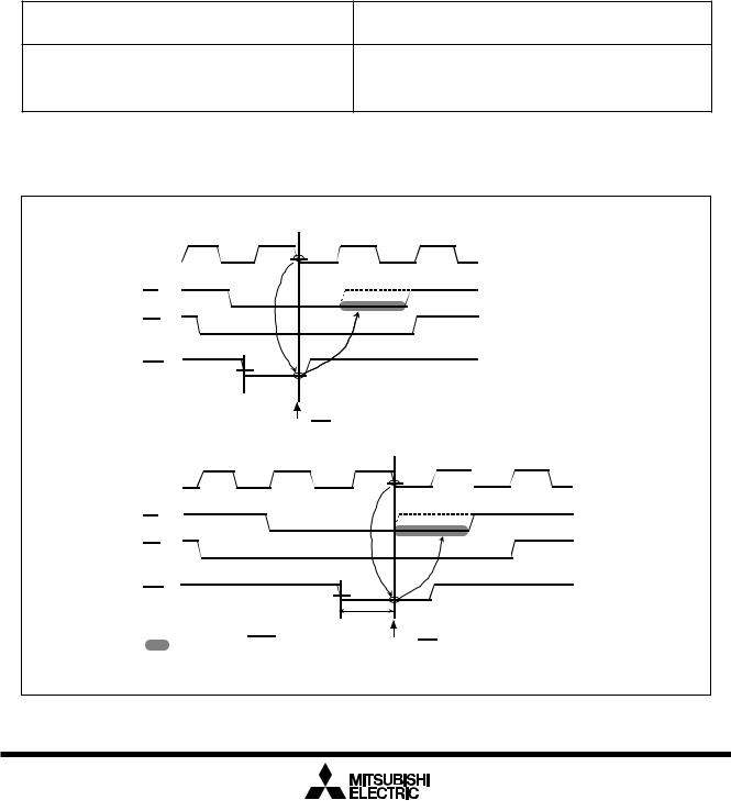
|
Mitsubishi microcomputers |
Bus Control |
M16C / 61 Group |
SINGLE-CHIP 16-BIT CMOS MICROCOMPUTER |
|
|
|
|
|
________
(5) The RDY signal
________
RDY is a signal that facilitates access to an external device that requires long access time. As shown in
________
Figure 1.11.3, if an “L” is being input to the RDY at the BCLK falling edge, the bus turns to the wait state.
________
If an “H” is being input to the RDY pin at the BCLK falling edge, the bus cancels the wait state. Table 1.11.4 shows the state of the microcomputer with the bus in the wait state, and Figure 1.11.3 shows an
example in which the RD signal is prolonged by the RDY signal.
________
The RDY signal is valid when accessing the external area during the bus cycle in which bits 4 to 7 of the
________
chip select control register (address 000816) are set to “0”. The RDY signal is invalid when setting “1” to all
________
bits 4 to 7 of the chip select control register (address 000816), but the RDY pin should be treated as properly as in non-using.
Table 1.11.4. Microcomputer status in ready state (Note)
Item |
|
Status |
Oscillation |
|
On |
___ |
_____ |
________ |
R/W signal, address bus, data bus, CS |
Maintain status when RDY signal received |
|
__________ |
|
|
ALE signal, HLDA, programmable I/O ports |
|
|
|
|
|
Internal peripheral circuits |
|
On |
________
Note: The RDY signal cannot be received immediately prior to a software wait.
In an instance of separate bus
BCLK
RD
CSi (i=0 to 3)
RDY

 tsu(RDY - BCLK)
Accept timing of RDY signal
In an instance of multiplexed bus
BCLK
RD
CSi (i=0 to 3)
RDY
:Wait using RDY signal
:Wait using software
tsu(RDY - BCLK)
Accept timing of RDY signal
_____ |
________ |
Figure 1.11.3. Example of RD signal extended by RDY signal
26
|
Mitsubishi microcomputers |
Bus Control |
M16C / 61 Group |
SINGLE-CHIP 16-BIT CMOS MICROCOMPUTER |
|
|
|
|
|
(6) Hold signal
The hold signal is used to transfer the bus privileges from the CPU to the external circuits. Inputting “L” to
__________
the HOLD pin places the microcomputer in the hold state at the end of the current bus access. This status is maintained and “L” is output from the HLDA pin as long as “L” is input to the HOLD pin. Table 1.11.5
shows the microcomputer status in the hold state.
__________
Bus-using priorities are given to HOLD, DMAC, and CPU in order of decreasing precedence.
|
__________ |
|
|
|
|
HOLD > DMAC > CPU |
|
|
|
||
Figure 1.11.4. Bus-using priorities |
|
||
Table 1.11.5. Microcomputer status in hold state |
|
||
|
|
|
|
|
Item |
Status |
|
|
|
|
|
Oscillation |
|
|
ON |
___ |
_____ _______ |
Floating |
|
R/W signal, address bus, data bus, CS, BHE |
|||
|
|
|
|
Programmable I/O ports |
|
P0, P1, P2, P3, P4, P5 |
Floating |
|
|
|
|
|
|
P6, P7, P8, P9, P10 |
Maintains status when hold signal is received |
__________ |
|
|
Output “L” |
HLDA |
|
|
|
|
|
|
|
Internal peripheral circuits |
|
|
ON (but watchdog timer stops) |
|
|
|
|
ALE signal |
|
|
Undefined |
|
|
|
|
(7) External bus status when the internal area is accessed
Table 1.11.6 shows the external bus status when the internal area is accessed.
Table 1.11.6. External bus status when the internal area is accessed
Item |
|
SFR accessed |
Internal ROM/RAM accessed |
|
Address bus |
|
Address output |
Maintain status before accessed |
|
|
||||
|
|
|
address of external area |
|
Data bus |
When read |
Floating |
Floating |
|
|
When write |
Output data |
Undefined |
|
RD, WR, WRL, WRH |
RD, WR, WRL, WRH output |
Output "H" |
||
BHE |
|
BHE output |
Maintain status before accessed |
|
|
||||
|
|
|
status of external area |
|
CS |
|
Output "H" |
Output "H" |
|
|
||||
ALE |
|
Output "L" |
Output "L" |
|
|
||||
27
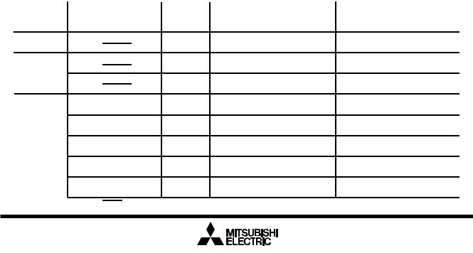
|
Mitsubishi microcomputers |
Bus Control |
M16C / 61 Group |
SINGLE-CHIP 16-BIT CMOS MICROCOMPUTER |
|
|
|
|
|
(8) BCLK output
The user can choose the BCLK output by use of bit 7 of processor mode register 0 (000416) (Note). When set to “1”, the output floating.
Note: Before attempting to change the contents of the processor mode register 0, set bit 1 of the protect register (address 000A16) to “1”.
(9) Software wait
A software wait can be inserted by setting the wait bit (bit 7) of the processor mode register 1 (address 000516) (Note) and bits 4 to 7 of the chip select control register (address 000816).
A software wait is inserted in the internal ROM/RAM area and in the external memory area by setting the wait bit of the processor mode register 1. When set to “0”, each bus cycle is executed in one BCLK cycle. When set to “1”, each bus cycle is executed in two or three BCLK cycles. After the microcomputer has been reset, this bit defaults to “0”. When set to “1”, a wait is applied to all memory areas (two or three BCLK cycles), regardless of the contents of bits 4 to 7 of the chip select control register. Set this bit after referring
to the recommended operating conditions (main clock input oscillation frequency) of the electric character-
________
istics. However, when the user is using the RDY signal, the relevant bit in the chip select control register’s bits 4 to 7 must be set to “0”.
When the wait bit of the processor mode register 1 is “0”, software waits can be set independently for each of the 4 areas selected using the chip select signal. Bits 4 to 7 of the chip select control register correspond to chip selects CS0 to CS3. When one of these bits is set to “1”, the bus cycle is executed in one BCLK cycle. When set to “0”, the bus cycle is executed in two or three BCLK cycles. These bits default to “0” after the microcomputer has been reset.
The SFR area is always accessed in two BCLK cycles regardless of the setting of these control bits. Also, insert a software wait if using the multiplex bus to access the external memory area.
Table 1.11.7 shows the software wait and bus cycles. Figure 1.11.5 shows example bus timing when using software waits.
Note: Before attempting to change the contents of the processor mode register 1, set bit 1 of the protect register (address 000A16) to “1”.
Table 1.11.7. Software waits and bus cycles
Area |
Bus status |
Wait bit |
Bits 4 to 7 of chip select |
|
Bus cycle |
control register |
|
||||
|
|
|
|
|
|
SFR |
|
Invalid |
Invalid |
2 |
BCLK cycles |
|
|||||
Internal |
|
0 |
Invalid |
1 |
BCLK cycle |
|
|||||
|
|
|
|
|
|
ROM/RAM |
|
1 |
Invalid |
2 |
BCLK cycles |
|
|
||||
|
Separate bus |
0 |
1 |
1 BCLK cycle |
|
|
|||||
External |
Separate bus |
0 |
0 |
2 |
BCLK cycles |
|
|
|
|
|
|
memory |
Separate bus |
1 |
0 (Note) |
2 BCLK cycles |
|
area |
|
|
|
|
|
|
Multiplex bus |
0 |
0 |
3 BCLK cycles |
|
|
Multiplex bus |
1 |
0 (Note) |
3 BCLK cycles |
|
|
|||||
|
|
|
|
|
|
Note: When using the RDY signal, always set to “0”.
28

|
Mitsubishi microcomputers |
Bus Control |
M16C / 61 Group |
SINGLE-CHIP 16-BIT CMOS MICROCOMPUTER |
|
|
|
|
|
< Separate bus (no wait) > |
Bus cycle |
|
|
|
|
BCLK
Write signal
Read signal
Data bus |
|
Output |
|
Input |
Address bus |
Address |
Address |
||
Chip select |
|
|
|
|
< Separate bus (with wait) >
|
|
|
|
|
Bus cycle |
||||
BCLK |
|
|
|
|
|
|
|
|
|
|
|
|
|
|
|
|
|
|
|
|
|
|
|
|
|
|
|
|
|
|
|
|
|
|
|
|
|
|
|
Write signal |
|
|
|
|
|
|
|
|
|
Read signal |
|
|
|
|
|
|
|
|
|
Data bus |
|
|
|
|
|
Output |
|||
Address bus |
|
|
|
|
|
|
|
||
|
|
|
|
Address |
|||||
Chip select |
|
|
|
|
|
|
|
|
|
< Multiplexed bus >
|
|
|
Bus cycle |
|||||||
BCLK |
|
|
|
|
|
|
|
|
|
|
|
|
|
|
|
|
|
|
|
|
|
|
|
|
|
|
|
|
|
|
|
|
|
|
|
|
|
|
|
|
|
|
|
Write signal |
|
|
|
|
|
|
|
|
|
|
Read signal |
|
|
|
|
|
|
|
|
|
|
ALE |
|
|
|
|
|
|
|
|
|
|
|
|
|
|
|
|
|
|
|
|
|
Address bus |
|
|
|
|
|
|
|
|
||
|
|
|
|
|
|
|
|
|||
|
|
|
Address |
|||||||
Address bus/ |
|
|
|
|
|
|
|
|
|
|
Address |
|
|
Data output |
|
|
|||||
Data bus |
|
|
|
|
||||||
|
|
|
|
|
|
|
|
|||
Chip select |
|
|
|
|
|
|
|
|
|
|
Input
Address
Address
 Address
 Input
Input
Figure 1.11.5. Typical bus timings using software wait
29
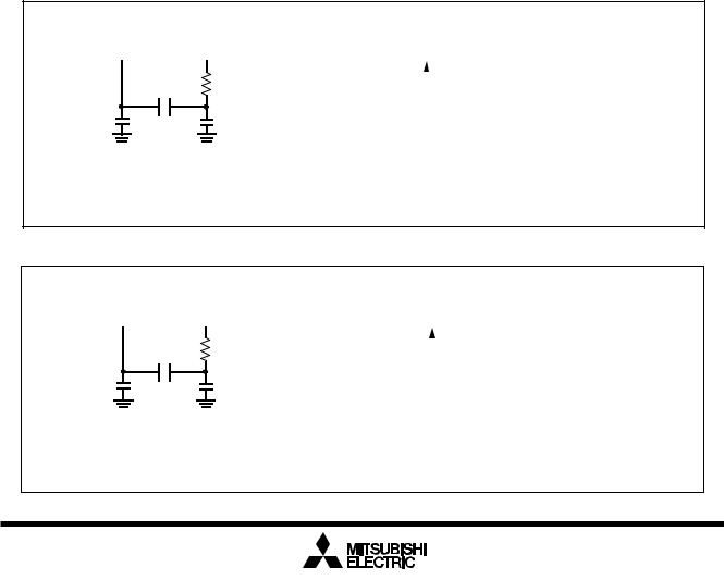
|
Mitsubishi microcomputers |
Clock Generating Circuit |
M16C / 61 Group |
SINGLE-CHIP 16-BIT CMOS MICROCOMPUTER |
|
|
|
|
|
Clock Generating Circuit
The clock generating circuit contains two oscillator circuits that supply the operating clock sources to the
CPU and internal peripheral units.
Table 1.12.1. Main clock and sub-clock generating circuits
|
Main clock generating circuit |
Sub-clock generating circuit |
|
|
|
Use of clock |
• CPU’s operating clock source |
• CPU’s operating clock source |
|
• Internal peripheral units’ |
• Timer A/B’s count clock |
|
operating clock source |
source |
|
|
|
Usable oscillator |
Ceramic or crystal oscillator |
Crystal oscillator |
|
|
|
Pins to connect oscillator |
XIN, XOUT |
XCIN, XCOUT |
|
|
|
Oscillation stop/restart function |
Available |
Available |
|
|
|
Oscillator status immediately after reset |
Oscillating |
Stopped |
|
|
|
Other |
Externally derived clock can be input |
|
|
|
|
Example of oscillator circuit
Figure 1.12.1 shows some examples of the main clock circuit, one using an oscillator connected to the circuit, and the other one using an externally derived clock for input. Figure 1.12.2 shows some examples of sub-clock circuits, one using an oscillator connected to the circuit, and the other one using an externally derived clock for input. Circuit constants in Figures 1.12.1 and 1.12.2 vary with each oscillator used. Use the values recommended by the manufacturer of your oscillator.
|
Microcomputer |
|
|
|
|
|
|
Microcomputer |
|
|
||||||||||
(Built-in feedback resistor) |
|
|
(Built-in feedback resistor) |
|
|
|||||||||||||||
XIN |
XOUT |
|
|
XIN |
|
|
|
|
XOUT |
|
|
|||||||||
|
|
|
|
|
|
|
|
|
|
|
|
|
|
|
|
|
|
|
|
|
|
|
|
|
|
(Note) |
|
|
|
|
|
|
|
|
Open |
|
|
||||
|
|
|
|
|
|
|
|
|
|
|
|
|
|
|
|
|
|
|
||
|
|
|
|
|
Rd |
|
|
|
|
|
|
|
|
|
|
|
|
|
|
|
|
|
|
|
|
|
|
|
|
|
|
|
|
|
|
|
|
|
|||
|
|
|
|
|
|
|
|
Externally derived clock |
|
|
||||||||||
|
|
|
|
|
|
|
|
|
|
|||||||||||
|
|
|
|
|
|
|
Vcc |
|
|
|
|
|
|
|
|
|
|
|
||
|
CIN |
|
COUT |
|
|
|
|
|
|
|
|
|
|
|
||||||
|
|
Vss |
|
|
|
|
|
|
|
|
|
|
|
|
||||||
|
|
|
|
|
|
|
|
|
|
|
|
|
|
|
|
|
|
|
||
|
|
|
|
|
|
|
|
|
|
|
|
|
|
|
|
|
|
|
||
Note: Insert a damping resistor if required. The resistance will vary depending on the oscillator and the oscillation drive capacity setting. Use the value recommended by the maker of the oscillator.
When the oscillation drive capacity is set to low, check that oscillation is stable. Also, if the oscillator manufacturer's data sheet specifies that a feedback resistor be added external to the chip, insert a feedback resistor between XIN and XOUT following the instruction.
Figure 1.12.1. Examples of main clock
Microcomputer |
|
|
|
Microcomputer |
|
|
|||||||||||
(Built-in feedback resistor) |
|
|
(Built-in feedback resistor) |
|
|
||||||||||||
XCIN |
|
XCOUT |
|
|
XCIN |
|
|
|
XCOUT |
|
|
||||||
|
|
|
|
|
|
|
|
|
|
|
|
|
|
|
|
|
|
|
|
(Note) |
|
|
|
|
|
|
|
|
Open |
|
|
||||
|
|
|
|
|
|
|
|
|
|
|
|
|
|
|
|
||
|
|
RCd |
|
|
|
|
|
|
|
|
|
|
|
|
|
|
|
|
|
|
|
|
|
|
|
|
|
|
|
|
|
|
|||
CCIN |
|
CCOUT |
|
Externally derived clock |
|
|
|||||||||||
|
|
|
|
||||||||||||||
|
Vcc |
|
|
|
|
|
|
|
|
|
|
|
|||||
|
|
|
|
|
|
|
|
|
|
|
|
||||||
|
|
|
|
|
|
|
|
|
|
|
|
|
|
|
|||
|
|
|
|
Vss |
|
|
|
|
|
|
|
|
|
|
|
|
|
|
|
|
|
|
|
|
|
|
|
|
|
|
|
|
|
||
Note: Insert a damping resistor if required. The resistance will vary depending on the oscillator and the oscillation drive capacity setting. Use the value recommended by the maker of the oscillator.
When the oscillation drive capacity is set to low, check that oscillation is stable. Also, if the oscillator manufacturer's data sheet specifies that a feedback resistor be added external to the chip, insert a feedback resistor between XCIN and XCOUT following the instruction.
Figure 1.12.2. Examples of sub-clock
30
Loading...