


Mitsubishi M30201M4T-XXXSP, M30201M4T-XXXFP, M30201M4-XXXSP, M30201M4-XXXFP, M30201M2T-XXXSP Datasheet
...Underdevelopment
Description
Mitsubishi microcomputers
M30201 Group
SINGLE-CHIP 16-BIT CMOS MICROCOMPUTER
Description
The M30201 group of single-chip microcomputers are built using the high-performance silicon gate CMOS process using a M16C/60 Series CPU core. M30201 group is packaged in a 52-pin plastic molded SDIP, or 56-pin plastic molded QFP. These single-chip microcomputers operate using sophisticated instructions featuring a high level of instruction efficiency. With 1M bytes of address space, they are capable of executing instructions at high speed.
The M30201 group includes a wide range of products with different internal memory types and sizes and various package types.
Features
• Basic machine instructions .................. |
Compatible with the M16C/60 series |
• Memory capacity.................................. |
ROM/RAM (See figure 1.4. ROM expansion.) |
• Shortest instruction execution time ...... |
100ns (f(XIN)=10MHz) |
• Supply voltage ..................................... |
4.0 to 5.5V (f(XIN)=10MHz) :mask ROM version |
|
2.7 to 5.5V (f(XIN)=7MHz with software one-wait):mask ROM |
|
version |
|
4.0 to 5.5V (f(XIN)=10MHz) :flash memory version |
• Interrupts.............................................. |
9 internal and 3 external interrupt sources, 4 software |
|
(including key input interrupt) |
• Multifunction 16-bit timer ...................... |
Timer A x 1, timer B x 2, timer X x 3 |
• Clock output |
|
• Serial I/O .............................................. |
1 channel for UART or clock synchronous, 1 for UART |
• A-D converter....................................... |
10 bits X 8 channels (Expandable up to 13 channels) |
• Watchdog timer .................................... |
1 line |
• Programmable I/O ............................... |
43 lines |
• LED drive ports .................................... |
8 ports |
• Clock generating circuit ....................... |
2 built-in clock generation circuits |
|
(built-in feedback resistor, and external ceramic or quartz oscillator) |
Applications
Home appliances, Audio, office equipment, Automobiles
Specifications written in this manual are believed to be accurate, but are not guaranteed to be entirely free of error.
Specifications in this manual may be changed for functional or performance improvements. Please make sure your manual is the latest edition.
------Table of Contents------
Central Processing Unit (CPU) ..................... |
12 |
Reset ............................................................. |
15 |
Clock Generating Circuit ............................... |
19 |
Protection ...................................................... |
26 |
Interrupts ....................................................... |
27 |
Watchdog Timer ............................................ |
35 |
Timer ............................................................. |
37 |
Serial I/O ....................................................... |
64 |
A-D Converter ............................................... |
78 |
Programmable I/O Ports ............................... |
88 |
Electric Characteristics ................................. |
95 |
Flash Memory version ................................. |
126 |
1
Underdevelopment
Description
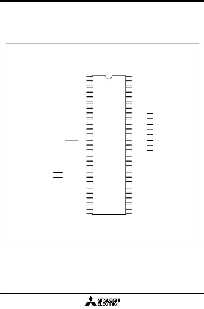
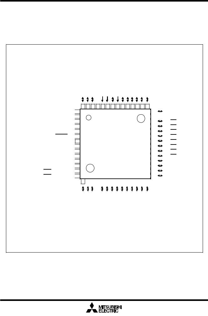
Pin Configuration
Figures 1.1 to 1.2 show the pin configurations (top view).
Mitsubishi microcomputers
M30201 Group
SINGLE-CHIP 16-BIT CMOS MICROCOMPUTER
PIN CONFIGURATION (top view)
AVSS 
 1
1
P60/AN0 
 2
2
VREF 
 3
3
AVCC 
 4
4
P54/CKOUT/AN54 
 5
5
P53/CLKS/AN53 
 6
6
P52/CLK0/AN52 
 7
7
P51/RXD0/AN51 
 8
8
P50/TXD0/AN50 
 9
9
CNVSS 
 10
10
P71/TB1IN/XCIN 
 11
11
P70/TB0IN/XCOUT 
 12
12
RESET 
 13
13
XOUT 
 14
14
VSS 
 15
15
XIN 
 16
16
VCC 
 17
17
P45/TX2INOUT 
 18
18
P44/INT1/TX1INOUT 
 19
19
P43/INT0/TX0INOUT 
 20
20
P42/RXD1 
 21
21
P41/TA0OUT 
 22
22
P40/TA0IN/TXD1
 23
23
P35 
 24
24
P34 
 25
25
P33 
 26
26
XXXSP-M30201MX XXXSP-M30201MXT M30201F6SP M30201F6TSP
52
 P61/AN1 51
 P62/AN2 50
 P63/AN3 49
 P64/AN4 48
 P65/AN5 47
 P66/AN6 46
 P67/AN7 45
 P00/KI0 44
 P01/KI1 43
 P02/KI2
42
 P03/KI3 41
 P04/KI4 40
 P05/KI5 39
 P06/KI6 38
 P07/KI7 37
 P10(LED0) 36
 P11(LED1) 35
 P12(LED2) 34
 P13(LED3) 33
 P14(LED4) 32
 P15(LED5) 31
 P16(LED6) 30
 P17(LED7) 29
 P30
P30
28
 P31
P31
27
 P32
P32
Package: 52P4B
Figure 1.1. Pin configuration for the M30201 group (shrink DIP product) (top view)
2
Underdevelopment
Description
Mitsubishi microcomputers
M30201 Group
SINGLE-CHIP 16-BIT CMOS MICROCOMPUTER
PIN CONFIGURATION (top view)
/AN52
/CLK0 P52
56
P51/RXD0/AN51 
 1
1
P50/TXD0/AN50 
 2
2
CNVSS
 3
3
P71/TB1IN/XCIN
 4
4
P70/TB0IN/XCOUT 
 5
5
RESET
 6
6
N.C. 7
XOUT
 8
8
VSS 
 9
9
XIN 
 10
10
VCC
 11
11
P45/TX2INOUT
 12
12
P44/INT1/TX1INOUT 
 13
13
P43/INT0/TX0INOUT 
 14
14
15
D1 /RX P42
P5/CLKS/AN353 |
P5/CK/AN4OUT54 |
|
N.C. |
|
AVCC |
|
VREF |
|
P6/AN00 |
|
AVSS |
|
P6/AN11 |
|
P6/AN22 |
|
P6/AN33 |
|
P6/AN44 |
|
P6/AN55 |
|
P6/AN66 |
|
|||
55 |
54 |
53 |
52 |
51 |
50 |
49 |
48 |
47 |
46 |
45 |
44 |
43 |
|
|
|
||||||||||||
|
|
|
|
|
|
|
|
|
|
|
|
|
|
|
|
|
|
|
|
|
|
|
|
|
|
42 |
P67/AN7 |
|
|
|
|
|
|
|
|
|
|
|
|
|
|
|
|
|
|
|
|
|
|
|
|
|
|
N.C. |
|
|
|
|
|
|
|
|
|
|
|
|
|
|
|
|
|
|
|
|
|
|
|
|
|
|
|
41 |
|
|
|
|
|
|
|
|
|
|
|
|
|
|
|
|
|
|
|
|
|
|
|
|
|
|
|
|
P00/KI0 |
|
|
|
|
|
|
|
|
|
|
|
|
|
|
|
|
|
|
|
|
|
|
|
40 |
||||
|
|
|
|
|
|
|
|
|
|
|
|
|
|
|
|
|
|
|
|
|
|
|
|
|
|
P01/KI1 |
|
|
|
|
|
|
|
|
|
|
|
|
|
|
|
|
|
|
|
|
|
|
|
|
|
|
|
39 |
|
|
|
|
|
|
|
|
|
|
|
|
|
|
|
|
|
|
|
|
|
|
|
|
|
|
|
P02/KI2 |
|
|
|
M30201MX-XXXFP |
|
|
|
|
|
38 |
|||||||||||||||||||
|
|
|
|
|
|
|
|
P03/KI3 |
|||||||||||||||||||
|
|
|
|
37 |
|||||||||||||||||||||||
|
|
M30201MXT-XXXFP |
|
|
|
P04/KI4 |
|||||||||||||||||||||
|
|
|
|
|
36 |
||||||||||||||||||||||
|
|
M30201F6FP |
|
|
|
|
|
|
|
|
|
|
|
P05/KI5 |
|||||||||||||
|
|
|
|
|
|
|
|
|
|
|
|
|
35 |
||||||||||||||
|
|
M30201F6TFP |
|
|
|
|
|
|
|
|
|
|
P06/KI6 |
||||||||||||||
|
|
|
|
|
|
|
|
34 |
|||||||||||||||||||
|
|
|
|
|
|
|
|
|
|
|
|
P07/KI7 |
|||||||||||||||
|
|
|
|
|
|
|
|
|
|
|
|
|
|
|
|
|
|
|
|
|
|
|
|
|
|
33 |
|
|
|
|
|
|
|
|
|
|
|
|
|
|
|
|
|
|
|
|
|
|
|
|
|
|
|
P10(LED0) |
|
|
|
|
|
|
|
|
|
|
|
|
|
|
|
|
|
|
|
|
|
|
|
|
|
|
|
32 |
|
|
|
|
|
|
|
|
|
|
|
|
|
|
|
|
|
|
|
|
|
|
|
|
|
|
|
|
P11(LED1) |
|
|
|
|
|
|
|
|
|
|
|
|
|
|
|
|
|
|
|
|
|
|
|
31 |
||||
|
|
|
|
|
|
|
|
|
|
|
|
|
|
|
|
|
|
|
|
|
|
|
|
|
|
P12(LED2) |
|
|
|
|
|
|
|
|
|
|
|
|
|
|
|
|
|
|
|
|
|
|
|
|
|
|
|
30 |
|
|
|
|
|
|
|
|
|
|
|
|
|
|
|
|
|
|
|
|
|
|
|
|
|
|
|
P13(LED3) |
|
|
|
|
|
|
|
|
|
|
|
|
|
|
|
|
|
|
|
|
|
|
|
|
|
|
|
29 |
|
16 |
|
17 |
|
18 |
|
19 |
|
20 |
|
21 |
|
22 |
|
23 |
|
24 |
|
25 |
|
26 |
|
27 |
|
28 |
|
|
|
P4/TA01OUT |
|
/TA0/TD0INX1 |
N.C. |
P35 |
P34 |
|
P33 |
|
P32 |
|
P31 |
|
P30 |
|
P1(LED)77 |
|
P1(LED)66 |
|
P1(LED)55 |
|
P1(LED)44 |
|
|||||
|
|
P4 |
|
|
|
|
|
|
|
|
|
|
|
|
|
|
|
|
|
|
|
|
|
|
|
|
|
Package: 56P6S-A
Figure 1.2. Pin configuration for the M30201 group (QFP product) (top view)
3
Underdevelopment
Description
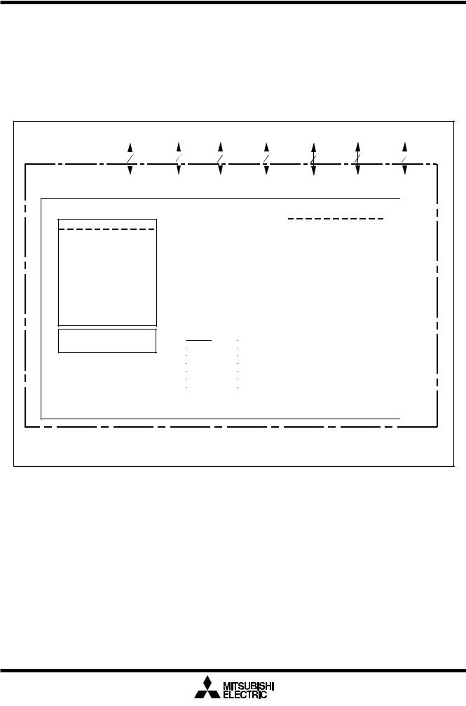
Block Diagram
Figure 1.3 is a block diagram of the M30201 group.
Mitsubishi microcomputers
M30201 Group
SINGLE-CHIP 16-BIT CMOS MICROCOMPUTER
I/O ports
|
|
8 |
|
8 |
|
6 |
|
6 |
5 |
8 |
|
|
2 |
|||||
|
||||||||||||||||||
|
|
|
|
|
|
|
|
|
|
|
|
|
|
|
|
|
|
|
|
|
|
|
|
|
|
|
|
|
|
|
|
|
|
|
|
|
|
Port P0 |
|
Port P1 |
|
Port P3 |
|
Port P4 |
|
Port P5 |
|
Port P6 |
|
Port P7 |
||||||
Internal peripheral functions
Timer
Timer TA0 (16 bits) Timer TB0 (16 bits) Timer TB1 (16 bits) Timer TX0 (16 bits) Timer TX1 (16 bits) Timer TX2 (16 bits)
Watchdog timer
(15 bits)
|
|
|
|
|
|
|
|
|
|
|
|
|
|
|
|
|
|
|
|
|
A-D converter |
|
|
System clock generator |
|
|
|||||||||||||
|
(10 bits X 8 channels |
|
|
|
|
|
XIN-XOUT |
|
|
||||||||||
Expandable up to 13 channels) |
|
|
|
|
XCIN-XCOUT |
|
|
||||||||||||
|
|
|
|
|
|
|
|
|
|
|
|
|
|
|
|
|
|
||
|
|
|
|
|
|
|
|
|
|
|
|
|
|
|
|
|
|
||
UART/clock synchronous SI/O |
|
|
|
|
|
|
|
|
|
||||||||||
|
(8 bits X 1 channel) |
|
|
|
|
|
|
|
|
|
|
||||||||
|
|
|
|
|
|
|
|
|
|
|
|
|
|
|
|
|
|
|
|
|
|
|
|
|
|
|
|
|
|
|
|
|
|
|
|
|
|
|
|
|
|
|
UART |
|
|
|
|
|
|
|
|
|
|
|
|
|
|
|
|
|
(8 bits X 1 channel) |
|
|
|
|
|
|
|
|
|
|
||||||||
|
|
|
|
|
|
|
|
|
|
|
|
|
|
|
|
|
|
||
|
|
|
|
|
|
|
|
|
|
|
|||||||||
|
M16C/60 series16-bit CPU core |
|
|
|
|
Memory |
|
|
|||||||||||
|
|
|
|
|
|
|
|
|
|
|
|
|
|
|
|
|
|
||
|
Registers |
|
|
|
|
Program counter |
|
|
|
|
ROM |
|
|
||||||
|
|
|
|
|
|
|
|
|
|
|
|
(Note 1) |
|
|
|||||
|
|
|
|
|
|
|
|
|
|
|
|
|
|
|
|
|
|
|
|
|
R0H |
|
R0L |
|
|
|
|
|
PC |
|
|
|
|
|
|
|
|||
|
R0H |
|
|
R0L |
|
|
|
|
|
|
|
|
|
|
|
|
RAM |
|
|
|
|
|
|
|
|
|
|
|
|
|
|
|
|
|
|
|
|||
|
R1H |
|
R1L |
|
|
|
|
|
|
|
|
|
|
|
|
|
|
||
|
R1H |
|
|
R1L |
|
|
|
|
|
Vector table |
|
|
|
|
(Note 2) |
|
|
||
|
|
|
|
|
|
|
|
|
|
|
|
|
|
||||||
|
R2 |
|
|
|
|
|
|
|
|
|
|
|
|
|
|||||
|
|
R2 |
|
|
|
|
|
|
|
|
|
|
|
|
|
|
|
|
|
|
R3 |
|
|
|
|
|
|
INTB |
|
|
|
|
|
|
|
||||
|
|
R3 |
|
|
|
|
|
|
|
|
|
|
|
|
|
|
|
|
|
|
|
|
|
|
|
|
|
|
|
|
|
|
|
|
|
|
|
||
|
A0 |
|
|
|
|
|
|
|
|
|
|
|
|
|
|
|
|
||
|
|
A0 |
|
|
|
|
|
|
Stack pointer |
|
|
|
|
|
|
|
|||
|
A1 |
|
|
|
|
|
|
|
|
|
|
|
|
|
|
|
|
||
|
|
A1 |
|
|
|
|
|
|
|
ISP |
|
|
|
|
|
|
|
||
|
FB |
|
|
|
|
|
|
|
|
|
|
|
|
|
|
||||
|
|
FB |
|
|
|
|
|
|
|
USP |
|
|
|
|
Multiplier |
|
|
||
|
|
|
|
|
|
|
|
|
|
|
|
|
|
|
|
|
|||
|
|
|
|
|
|
|
|
|
|
|
|
|
|
|
|
|
|
|
|
|
|
|
|
|
|
|
|
|
|
|
|
|
|
|
|
|
|
||
|
|
SB |
|
|
|
|
|
|
|
FLG |
|
|
|
|
|
|
|
||
|
|
|
|
|
|
|
|
|
|
|
|
|
|
|
|
|
|
|
|
Note 1: ROM size depends on MCU type.
Note 2: RAM size depends on MCU type.
Figure 1.3. Block diagram for the M30201 group
4

Underdevelopment
Description
Mitsubishi microcomputers
M30201 Group
SINGLE-CHIP 16-BIT CMOS MICROCOMPUTER
Performance Outline
Table 1.1 is performance outline of M30201 group.
Table 1.1. Performance outline of M30201 group
|
|
|
Item |
Performance |
|
|
|
|
|
Number of basic instructions |
91 instructions |
|||
|
|
|
|
|
Shortest instruction execution time |
100ns (f(XIN)=10MHz |
|||
|
|
|
|
|
Memory |
|
ROM |
(See figure 4. ROM expansion.) |
|
|
|
|
|
|
capacity |
|
RAM |
(See figure 4. ROM expansion.) |
|
|
|
|
|
|
I/O port |
|
P0 to P7 |
43 lines |
|
|
|
|
|
|
Multifunction |
|
TA0 |
16 bits x 1 |
|
|
|
|
|
|
timer |
|
TB0, TB1 |
16 bits x 2 |
|
|
|
|
|
|
|
|
|
TX0, TX1, TX2 |
16 bits x 3 |
|
|
|
|
|
Serial I/O |
|
UART0 |
(UART or clock synchronous) x 1 |
|
|
|
|
UART1 |
UART x 1 |
|
|
|
|
|
A-D converter |
|
10 bits x 8 channels (Expandable up to 13 channels) |
||
|
|
|
|
|
Watchdog timer |
15 bits x 1 (with prescaler) |
|||
|
|
|
|
|
Interrupt |
|
9 internal and 3 external sources, 4 software sources |
||
|
|
|
|
|
Clock generating circuit |
2 built-in clock generation circuits |
|||
|
|
|
|
(built-in feedback resistor, and external ceramic or |
|
|
|
|
quartz oscillator) |
|
|
|
|
|
Supply voltage |
|
4.0 to 5.5V (f(XIN)=10MHz) :mask ROM version |
||
|
|
|
|
2.7 to 5.5V (f(XIN)=7MHz with software one-wait) :mask |
|
|
|
|
ROM version |
|
|
|
|
4.0 to 5.5V (f(XIN)=10MHz) :flash memory version |
|
|
|
|
|
Power consumption |
18mW (f(XIN)=7MHz with software one-wait, Vcc=3V) |
|||
|
|
|
|
:mask ROM version |
|
|
|
|
95mW (f(XIN)=10MHz no wait, Vcc=5V) :flash memory version |
|
|
|
|
|
I/O |
|
I/O withstand voltage |
5V |
|
|
|
|
|
|
characteristics |
|
Output current |
5mA (15mA:LED drive port) |
|
|
|
|
|
|
Device configuration |
CMOS silicon gate |
|||
|
|
|
|
|
Package |
|
52-pin plastic mold SDIP |
||
|
|
|
|
56-pin plastic mold QFP |
|
|
|
|
|
5

Underdevelopment
Description
Mitsubishi microcomputers
M30201 Group
SINGLE-CHIP 16-BIT CMOS MICROCOMPUTER
Mitsubishi plans to release the following products in the M30201 group:
(1)Support for mask ROM version and flash memory version
(2)ROM capacity
(3)Package
52P4B : Plastic molded SDIP (mask ROM version and flash memory version) 56P6S-A : Plastic molded QFP (mask ROM version and flash memory version)
July 1998
RAM Size
(Byte)
M30201F6SP/FP
2K
|
|
|
M30201F6TSP/FP |
|
|
|
|
Under development |
|
|
|
M30201M4-XXXSP/FP |
|
|
1K |
|
M30201M4T-XXXSP/FP |
|
|
|
|
Under development |
|
|
512 |
M30201M2-XXXSP/FP |
|
|
|
M30201M2T-XXXSP/FP |
|
|
|
|
|
|
|
|
|
|
Under planning |
|
|
|
|
16K |
32K |
48K |
ROM Size |
|
|
|
|
(Byte) |
Figure 1.4. ROM expansion
Type No. M 3 0 2 0 1 M 4 T – X X X S P
Package type:
SP : Package 52P4B
FP : Package 56P6S-A
ROM No.
Omitted for flash memory version
Shows difference of characteristics and usage etc:
Nothing : Common
T : Automobiles
ROM capacity: 2 : 16K bytes 4 : 32K bytes 6 : 48K bytes
Memory type:
M : Mask ROM version
F : Flash memory version
Shows pin count, etc
(The value itself has no specific meaning)
M16C/20 Group
M16C Family
Figure 1.5. Type No., memory size, and package
6
Underdevelopment
Pin Description
Mitsubishi microcomputers
M30201 Group
SINGLE-CHIP 16-BIT CMOS MICROCOMPUTER
Pin Description
Pin name |
Signal name |
I/O type |
VCC, VSS |
Power supply |
|
|
input |
|
CNVSS |
CNVSS |
Input |
RESET |
Reset input |
Input |
XIN |
Clock input |
Input |
XOUT |
Clock output |
Output |
AVCC |
Analog power |
|
|
supply input |
|
AVSS |
Analog power |
|
|
supply input |
|
VREF |
Reference |
Input |
|
voltage input |
|
P00 to P07 |
I/O port P0 |
Input/output |
P10 to P17 |
I/O port P1 |
Input/output |
P30 to P35 |
I/O port P3 |
Input/output |
P40 to P45 |
I/O port P4 |
Input/output |
Function
Supply 2.7 to 5.5 V to the VCC pin. Supply 0 V to the VSS pin.
Connect it to the VSS pin.
A “L” on this input resets the microcomputer.
These pins are provided for the main clock generating circuit. Connect a ceramic resonator or crystal between the XIN and the XOUT pins. To use an externally derived clock, input it to the XIN pin and leave the XOUT pin open.
This pin is a power supply input for the A-D converter. Connect it to VCC.
This pin is a power supply input for the A-D converter. Connect it to VSS.
This pin is a reference voltage input for the A-D converter.
This is an 8-bit CMOS I/O port. It has an input/output port direction register that allows the user to set each pin for input or output individually. When set for input, the user can specify in units of four bits via software whether or not they are tied to a pull-up resistor.
This is an 8-bit I/O port equivalent to P0.
This is a 6-bit I/O port equivalent to P0.
This is a 6-bit I/O port equivalent to P0. The P40 pin is shared with timer A0 input and serial I/O output TxD1. The P41 pin is shared with timer A0 output. The P42 pin is shared with serial I/O input RxD1. The P43 pin is shared with external interrupt INT0 and timer X0 input/output TX0INOUT. The P44 pin is shared with external interrupt INT1 and timer X1 input/output TX1INOUT. The P45 pin is shared with timer X2 input/output TX2INOUT.
P50 to P54 |
I/O port P5 |
Input/output |
P60 to P67 |
I/O port P6 |
Input/output |
P70 to P71 |
I/O port P7 |
Input/output |
This is a 5-bit I/O port equivalent to P0. The P50, P51, P52, and P53 pins are shared with serial I/O pins TxD0, RxD0, CLK0, and CLKS. The P54 pin is shared with clock output CLKOUT. Also, these pins are shared with analog input pins AN50 through AN54.
This is an 8-bit I/O port equivalent to P0. These pins are shared with analog input pins AN0 through AN7.
This is a 2-bit I/O port equivalent to P0 . These pins are used for input/output to and from the oscillator circuit for the clock. Connect a crystal oscillator between the XCIN and the XCOUT pins.
7
Underdevelopment
Memory
Mitsubishi microcomputers
M30201 Group
SINGLE-CHIP 16-BIT CMOS MICROCOMPUTER
Operation of Functional Blocks
The M30201 accommodates certain units in a single chip. These units include ROM and RAM to store instructions and data and the central processing unit (CPU) to execute arithmetic/logic operations. Also included are peripheral units such as timers, serial I/O, A-D converter, and I/O ports.
The following explains each unit.
Memory
Figure 1.6 is a memory map of the M30201. The address space extends the 1M bytes from address 0000016 to FFFFF16. From FFFFF16 down is ROM. For example, in the M30201M4-XXXFP, there is 32K bytes of internal ROM from F800016 to FFFFF16. The vector table for fixed interrupts such as the reset are mapped to FFFDC16 to FFFFF16. The starting address of the interrupt routine is stored here. The address of the vector table for timer interrupts, etc., can be set as desired using the internal register (INTB). See the section on interrupts for details.
From 0040016 up is RAM. For example, in the M30201M4-XXXFP, there is 1K byte of internal RAM from 0040016 to 007FF16. In addition to storing data, the RAM also stores the stack used when calling subroutines and when interrupts are generated.
The SFR area is mapped to 0000016 to 003FF16. This area accommodates the control registers for peripheral devices such as I/O ports, A-D converter, serial I/O, and timers, etc. Any part of the SFR area that is not occupied is reserved and cannot be used for other purposes.
The special page vector table is mapped to FFE0016 to FFFDB16. If the starting addresses of subroutines or the destination addresses of jumps are stored here, subroutine call instructions and jump instructions can be used as 2-byte instructions, reducing the number of program steps.
0000016
SFR area For details, see Figures 1.7 to 1.8
0040016
Internal RAM area
YYYYY16
Type No. |
Address |
Address |
|
||
XXXXX16 |
YYYYY16 |
|
|
||
|
|
||||
M30201M4 |
F800016 |
007FF16 |
|
|
|
|
|||||
M30201M2 |
FC00016 |
005FF16 |
|
||
|
|||||
M30201F6 |
F400016 |
00BFF16 |
XXXXX16 |
||
Internal ROM area |
|||||
|
|
|
|||
|
|
|
|||
|
|
|
FFFFF16 |
|
|
FFE0016 |
|
Special page |
|
|
|
|
|
||
|
|
vector table |
|
|
FFFDC16 |
|
|
|
|
|
Undefined instruction |
|||
|
|
|||
|
|
Overflow |
|
|
|
|
|
||
|
|
BRK instruction |
|
|
|
|
Address match |
|
|
|
|
Single step |
|
|
|
|
Watchdog timer |
||
|
|
|||
|
|
DBC |
|
|
|
|
|
||
FFFFF16 |
|
Reset |
||
|
|
|
|
|
Figure 1.6. Memory map
8

Underdevelopment
Memory
Mitsubishi microcomputers
M30201 Group
SINGLE-CHIP 16-BIT CMOS MICROCOMPUTER
000016
000116
000216
000316
000416
000516
000616
000716
000816
000916
000A16
000B16
000C16
000D16
000E16
000F16
001016
001116
001216
001316
001416
001516
001616
001716
001816
001916
001A16
001B16
001C16
001D16
001E16
001F16
002016
002116
002216
002316
002416
002516
002616
002716
002816
002916
002A16
002B16
002C16
002D16
002E16
002F16
003016
003116
003216
003316
003416
003516
003616
003716
003816
003916
003A16
003B16
003C16
003D16
003E16
003F16
Processor mode register 0 (PM0) Processor mode register 1(PM1) System clock control register 0 (CM0) System clock control register 1 (CM1)
Address match interrupt enable register (AIER) Protect register (PRCR)
Watchdog timer start register (WDTS) Watchdog timer control register (WDC)
Address match interrupt register 0 (RMAD0)
Address match interrupt register 1 (RMAD1)
004016
004116
004216
004316
004416
004516
004616
004716
004816
004916
004A16
004B16
004C16
004D16
004E16
004F16
005016
005116
005216
005316
005416
005516
005616
005716
005816
005916
005A16
005B16
005C16
005D16
005E16
005F16
Key input interrupt control register (KUPIC) A-D conversion interrupt control register (ADIC)
UART0 transmit interrupt control register (S0TIC) UART0 receive interrupt control register (S0RIC) UART1 transmit interrupt control register (S1TIC) UART1 receive interrupt control register (S1RIC)
Timer A0 interrupt control register (TA0IC) Timer X0 interrupt control register (TX0IC) Timer X1 interrupt control register (TX1IC) Timer X2 interrupt control register (TX2IC)
Timer B0 interrupt control register (TB0IC) Timer B1 interrupt control register (TB1IC)
INT0 interrupt control register (INT0IC) INT1 interrupt control register (INT1IC)
Figure 1.7. Location of peripheral unit control registers (1)
9

Underdevelopment
Memory
038016 |
Count start flag (TABSR) |
|
038116 |
Clock prescaler reset flag (CPSRF) |
|
038216 |
One-shot start flag (ONSF) |
|
038316 |
Trigger select register (TRGSR) |
|
038416 |
Up-down flag (UDF) |
|
038516 |
|
|
038616 |
Timer A0 (TA0) |
|
038716 |
|
|
|
|
|
038816 |
Timer X0 (TX0) |
|
038916 |
|
|
|
|
|
038A16 |
Timer X1 (TX1) |
|
038B16 |
|
|
038C16 |
Timer X2 (TX2) |
|
038D16 |
|
|
|
|
|
038E16 |
Clock divided counter (CDC) |
|
038F16 |
|
|
039016 |
Timer B0 (TB0) |
|
039116 |
|
|
039216 |
Timer B1 (TB1) |
|
039316 |
|
|
039416 |
|
|
039516 |
|
|
039616 |
Timer A0 mode register (TA0MR) |
|
039716 |
Timer X0 mode register (TX0MR) |
|
039816 |
Timer X1 mode register (TX1MR) |
|
039916 |
Timer X2 mode register (TX2MR) |
|
039A16 |
|
|
039B16 |
Timer B0 mode register (TB0MR) |
|
039C16 |
Timer B1 mode register (TB1MR) |
|
039D16 |
|
|
039E16 |
|
|
039F16 |
|
|
03A016 |
UART0 transmit/receive mode register (U0MR) |
|
03A116 |
UART0 bit rate generator (U0BRG) |
|
03A216 |
UART0 transmit buffer register (U0TB) |
|
03A316 |
|
|
03A416 |
UART0 transmit/receive control register 0 (U0C0) |
|
03A516 |
UART0 transmit/receive control register 1 (U0C1) |
|
03A616 |
UART0 receive buffer register (U0RB) |
|
03A716 |
|
|
03A816 |
UART1 transmit/receive mode register (U1MR) |
|
03A916 |
UART1 bit rate generator (U1BRG) |
|
03AA16 |
UART1 transmit buffer register (U1TB) |
|
03AB16 |
|
|
03AC16 |
UART1 transmit/receive control register 0 (U1C0) |
|
03AD16 |
UART1 transmit/receive control register 1 (U1C1) |
|
03AE16 |
UART1 receive buffer register (U1RB) |
|
03AF16 |
|
|
03B016 |
UART transmit/receive control register 2 (UCON) |
|
03B116 |
|
|
|
|
|
03B216 |
|
|
03B316 |
|
|
|
|
|
|
Flash memory control register 0 (FCON0) (Note) |
|
03B416 |
|
|
03B516 |
Flash memory control register 1 (FCON1) (Note) |
|
03B616 |
Flash command register (FCMD) (Note) |
|
03B716 |
|
|
03B816 |
|
|
03B916 |
|
|
03BA16 |
|
|
03BB16 |
|
|
03BC16 |
|
|
|
|
|
03BD16 |
|
|
03BE16 |
|
|
03BF16 |
|
|
|
Note: This register is only exist in flash memory version. |
|
10
Mitsubishi microcomputers
M30201 Group
SINGLE-CHIP 16-BIT CMOS MICROCOMPUTER
03C016 |
A-D register 0 (AD0) |
|
03C116 |
||
|
||
03C216 |
A-D register 1 (AD1) |
|
03C316 |
||
|
||
03C416 |
A-D register 2 (AD2) |
|
03C516 |
||
|
||
03C616 |
A-D register 3 (AD3) |
|
03C716 |
||
|
||
03C816 |
A-D register 4 (AD4) |
|
03C916 |
||
|
||
03CA16 |
A-D register 5 (AD5) |
|
03CB16 |
||
|
||
03CC16 |
A-D register 6 (AD6) |
|
03CD16 |
|
|
03CE16 |
A-D register 7 (AD7) |
|
03CF16 |
||
|
||
03D016 |
|
|
03D116 |
|
|
|
||
03D216 |
|
|
03D316 |
|
|
03D416 |
A-D control register 2 (ADCON2) |
|
03D516 |
|
|
03D616 |
A-D control register 0 (ADCON0) |
|
03D716 |
A-D control register 1 (ADCON1) |
|
03D816 |
|
|
03D916 |
|
|
03DA16 |
|
|
03DB16 |
|
|
03DC16 |
|
|
03DD16 |
|
|
03DE16 |
|
|
03DF16 |
|
|
03E016 |
Port P0 (P0) |
|
03E116 |
Port P1 (P1) |
|
03E216 |
Port P0 direction register (PD0) |
|
03E316 |
Port P1 direction register (PD1) |
|
03E416 |
Port P2 (P2) (Reserved) |
|
03E516 |
Port P3 (P3) |
|
03E616 |
Port P2 direction register (PD2) (Reserved) |
|
03E716 |
Port P3 direction register (PD3) |
|
03E816 |
Port P4 (P4) |
|
03E916 |
Port P5 (P5) |
|
03EA16 |
Port P4 direction register (PD4) |
|
03EB16 |
Port P5 direction register (PD5) |
|
03EC16 |
Port P6 (P6) |
|
03ED16 |
Port P7 (P7) |
|
03EE16 |
Port P6 direction register (PD6) |
|
03EF16 |
Port P7 direction register (PD7) |
|
03F016 |
|
|
03F116 |
|
|
03F216 |
|
|
03F316 |
|
|
03F416 |
|
|
03F516 |
|
|
03F616 |
|
|
03F716 |
|
|
03F816 |
|
|
03F916 |
|
|
03FA16 |
|
|
03FB16 |
|
03FC16 |
Pull-up control register 0 (PUR0) |
03FD16 |
Pull-up control register 1 (PUR1) |
03FE16 Port P1 drive control register (DRR)
03FF16
Underdevelopment
CPU
Mitsubishi microcomputers
M30201 Group
SINGLE-CHIP 16-BIT CMOS MICROCOMPUTER
Central Processing Unit (CPU)
The CPU has a total of 13 registers shown in Figure 1.9. Seven of these registers (R0, R1, R2, R3, A0, A1, and FB) come in two sets; therefore, these have two register banks.
|
b15 |
|
b8 b7 |
|
b0 |
|
||
R0(Note) |
|
|
H |
|
L |
|
||
|
b15 |
|
b8 b7 |
|
b0 |
|
||
R1(Note) |
|
|
H |
|
L |
|
||
|
|
|
||||||
b15 |
|
|
|
|
b0 |
|
||
R2(Note) |
|
|
|
|
|
|
|
|
|
|
|
|
|
|
|
|
|
b15 |
|
|
|
|
b0 |
|
||
R3(Note) |
|
|
|
|
|
|
|
|
|
|
|
|
|
|
|
|
|
b15 |
|
|
|
|
b0 |
|
||
A0(Note) |
|
|
|
|
|
|
|
|
|
|
|
|
|
|
|
|
|
b15 |
|
|
|
|
b0 |
|
||
A1(Note) |
|
|
|
|
|
|
|
|
|
|
|
|
|
|
|
|
|
b15 |
|
|
|
|
b0 |
|
||
FB(Note) |
|
|
|
|
|
|
|
|
|
|
|
|
|
|
|
|
|
|
|
b19 |
|
|
|
|
b0 |
|||
PC |
|
|
|
|
|
|
|
|
Program counter |
|
Data |
|
|
|
|
|
|
|
|
|
|
|
|
|
|
|
|
|
|
|
||
registers |
b19 |
|
|
|
|
b0 |
||||
|
|
|
|
|
|
|||||
INTB |
|
|
|
|
|
|
|
|
|
Interrupt table |
|
|
H |
|
|
L |
|
|
|
||
|
|
|
|
|
|
|
|
|
|
register |
|
|
|
|
b15 |
|
|
|
|||
|
|
|
|
|
b0 |
|||||
|
|
USP |
|
|
|
|
|
|
User stack pointer |
|
|
|
|
|
|
|
|
|
|
|
|
|
|
|
|
b15 |
|
b0 |
||||
|
|
ISP |
|
|
|
|
|
|
Interrupt stack |
|
|
|
|
|
|
|
|
|
|||
Address |
|
|
|
|
|
|
|
|
pointer |
|
|
|
|
|
|
|
|
|
|||
|
|
|
|
|
|
|
|
|
||
registers |
|
|
b15 |
|
b0 |
|||||
|
|
SB |
|
|
|
|
|
|
Static base |
|
|
|
|
|
|
|
|
|
|||
|
|
|
|
|
|
|
|
|
|
register |
|
|
|
|
|
b15 |
|
|
|
||
|
|
|
|
|
|
|
b0 |
|||
Frame base |
FLG |
|
|
|
|
|
|
Flag register |
||
registers |
|
|
|
|
|
|
|
|
|
|
|
|
|
|
|
|
|
|
|
||
|
IPL |
U |
I |
O |
B |
S |
Z |
D |
C |
|
|
|
|
|
|
|
|
|
|
Note: These registers consist of two register banks.
Figure 1.9. Central processing unit register
(1) Data registers (R0, R0H, R0L, R1, R1H, R1L, R2, and R3)
Data registers (R0, R1, R2, and R3) are configured with 16 bits, and are used primarily for transfer and arithmetic/logic operations.
Registers R0 and R1 each can be used as separate 8-bit data registers, high-order bits as (R0H, R1H), and low-order bits as (R0L, R1L). In some instructions, registers R2 and R0, as well as R3 and R1 can use as 32-bit data registers (R2R0, R3R1).
(2) Address registers (A0 and A1)
Address registers (A0 and A1) are configured with 16 bits, and have functions equivalent to those of data registers. These registers can also be used for address register indirect addressing and address register relative addressing.
In some instructions, registers A1 and A0 can be combined for use as a 32-bit address register (A1A0).
11

Underdevelopment
CPU
Mitsubishi microcomputers
M30201 Group
SINGLE-CHIP 16-BIT CMOS MICROCOMPUTER
(3) Frame base register (FB)
Frame base register (FB) is configured with 16 bits, and is used for FB relative addressing.
(4) Program counter (PC)
Program counter (PC) is configured with 20 bits, indicating the address of an instruction to be executed.
(5) Interrupt table register (INTB)
Interrupt table register (INTB) is configured with 20 bits, indicating the start address of an interrupt vector table.
(6) Stack pointer (USP/ISP)
Stack pointer comes in two types: user stack pointer (USP) and interrupt stack pointer (ISP), each configured with 16 bits.
Your desired type of stack pointer (USP or ISP) can be selected by a stack pointer select flag (U flag). This flag is located at the position of bit 7 in the flag register (FLG).
(7) Static base register (SB)
Static base register (SB) is configured with 16 bits, and is used for SB relative addressing.
(8) Flag register (FLG)
Flag register (FLG) is configured with 11 bits, each bit is used as a flag. Figure 1.10 shows the flag register (FLG). The following explains the function of each flag:
•Bit 0: Carry flag (C flag)
This flag retains a carry, borrow, or shift-out bit that has occurred in the arithmetic/logic unit.
•Bit 1: Debug flag (D flag)
This flag enables a single-step interrupt.
When this flag is “1”, a single-step interrupt is generated after instruction execution. This flag is cleared to “0” when the interrupt is acknowledged.
•Bit 2: Zero flag (Z flag)
This flag is set to “1” when an arithmetic operation resulted in 0; otherwise, cleared to “0”.
•Bit 3: Sign flag (S flag)
This flag is set to “1” when an arithmetic operation resulted in a negative value; otherwise, cleared to “0”.
•Bit 4: Register bank select flag (B flag)
This flag chooses a register bank. Register bank 0 is selected when this flag is “0” ; register bank 1 is selected when this flag is “1”.
•Bit 5: Overflow flag (O flag)
This flag is set to “1” when an arithmetic operation resulted in overflow; otherwise, cleared to “0”.
•Bit 6: Interrupt enable flag (I flag)
This flag enables a maskable interrupt.
An interrupt is disabled when this flag is “0”, and is enabled when this flag is “1”. This flag is cleared to “0” when the interrupt is acknowledged.
12
Underdevelopment
CPU
Mitsubishi microcomputers
M30201 Group
SINGLE-CHIP 16-BIT CMOS MICROCOMPUTER
•Bit 7: Stack pointer select flag (U flag)
Interrupt stack pointer (ISP) is selected when this flag is “0” ; user stack pointer (USP) is selected when this flag is “1”.
This flag is cleared to “0” when a hardware interrupt is acknowledged or an INT instruction of software interrupt Nos. 0 to 31 is executed.
•Bits 8 to 11: Reserved area
•Bits 12 to 14: Processor interrupt priority level (IPL)
Processor interrupt priority level (IPL) is configured with three bits, for specification of up to eight processor interrupt priority levels from level 0 to level 7.
If a requested interrupt has priority greater than the processor interrupt priority level (IPL), the interrupt is enabled.
•Bit 15: Reserved area
The C, Z, S, and O flags are changed when instructions are executed. See the software manual for
details.
|
b15 |
|
b8 b7 |
|
|
b0 |
|
||
R0(Note) |
|
|
H |
|
|
L |
|
||
|
b15 |
|
b8 b7 |
|
|
b0 |
|
||
R1(Note) |
|
|
H |
|
|
L |
|
||
|
|
|
|
||||||
b15 |
|
|
|
|
|
b0 |
|
||
R2(Note) |
|
|
|
|
|
|
|
|
|
|
|
|
|
|
|
|
|
|
|
b15 |
|
|
|
|
|
b0 |
|
||
R3(Note) |
|
|
|
|
|
|
|
|
|
|
|
|
|
|
|
|
|
|
|
b15 |
|
|
|
|
|
b0 |
|
||
A0(Note) |
|
|
|
|
|
|
|
|
|
|
|
|
|
|
|
|
|
|
|
b15 |
|
|
|
|
|
b0 |
|
||
A1(Note) |
|
|
|
|
|
|
|
|
|
|
|
|
|
|
|
|
|
|
|
b15 |
|
|
|
|
|
b0 |
|
||
FB(Note) |
|
|
|
|
|
|
|
|
|
|
|
|
|
|
|
|
|
|
|
|
|
|
|
b19 |
|
|
|
|
|
|
|
|
b0 |
|||||||
|
|
|
PC |
|
|
|
|
|
|
|
|
|
|
|
|
|
|
|
|
Program coun |
Data |
|
|
|
|
|
|
|
|
|
|
|
|
|
|
|
|
|
|||
|
|
|
|
|
|
|
|
|
|
|
|
|
|
|
|
|
||||
registers |
b19 |
|
|
|
|
|
|
|
|
b0 |
||||||||||
|
|
|
|
|
|
|
|
|
|
|
|
|||||||||
|
|
|
INTB |
|
H |
|
|
|
|
L |
|
|
|
|
Interrupt table |
|||||
|
|
|
|
|
|
|
|
|
|
|
|
|
|
|
|
|
|
|
|
register |
|
|
|
|
|
|
b15 |
|
|
|
|
|
|
|
|
|
|
||||
|
|
|
|
|
|
|
|
|
|
|
|
|
|
b0 |
||||||
|
|
|
|
USP |
|
|
|
|
|
|
|
|
|
|
|
|
|
User stack po |
||
|
|
|
|
|
|
|
|
|
|
|
|
|
|
|
|
|
|
|
|
|
|
|
|
|
|
|
b15 |
|
|
|
|
|
|
|
|
b0 |
|||||
|
|
|
|
|
|
|
|
|
|
|
|
|
|
|
|
|
|
|
|
Interrupt stac |
|
|
|
|
ISP |
|
|
|
|
|
|
|
|
|
|
|
|
|
|||
Address |
|
|
|
|
|
|
|
|
|
|
|
|
|
|
|
|
pointer |
|||
|
|
|
|
|
|
|
|
|
|
|
|
|
|
|
|
|||||
|
|
|
|
|
|
|
|
|
|
|
|
|
|
|
|
|
||||
registers |
|
|
b15 |
|
|
|
|
|
|
|
|
b0 |
||||||||
|
|
|
|
SB |
|
|
|
|
|
|
|
|
|
|
|
|
|
Static base |
||
|
|
|
|
|
|
|
|
|
|
|
|
|
|
|
|
|
||||
|
|
|
|
|
|
|
|
|
|
|
|
|
|
|
|
|
|
|
|
register |
|
|
|
|
|
|
|
b15 |
|
|
|
|
|
|
|
|
|
|
|||
|
|
|
|
|
|
|
|
|
|
|
|
|
|
|
|
b0 |
||||
Frame base |
FLG |
|
|
|
|
|
|
|
|
|
|
|
|
Flag register |
||||||
registers |
|
|
|
|
|
|
|
|
|
|
|
|
|
|
|
|
|
|||
|
|
|
|
|
|
|
|
|
|
|
|
|
|
|
|
|
||||
|
|
|
|
|
|
|
|
|
|
|
|
|
|
|
|
|
||||
|
IPL |
|
|
|
|
U |
I |
|
|
O |
B |
S |
Z |
D |
C |
|
||||
|
|
|
|
|
|
|
|
|
|
|
|
|
|
|
|
|
|
|
|
|
Figure 1.10. Flag register (FLG)
13
Underdevelopment
Reset
Mitsubishi microcomputers
M30201 Group
SINGLE-CHIP 16-BIT CMOS MICROCOMPUTER
Reset
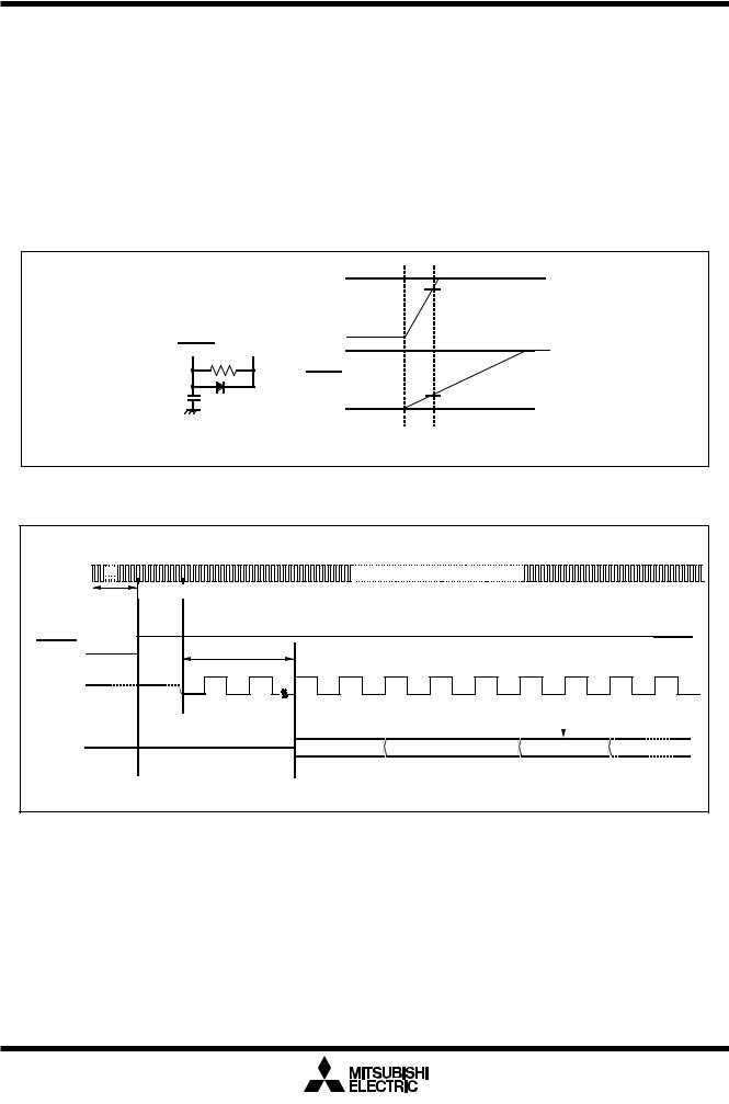
There are two kinds of resets; hardware and software. In both cases, operation is the same after the reset. (See “Software Reset” for details of software resets.) This section explains on hardware resets.
When the supply voltage is in the range where operation is guaranteed, a reset is effected by holding the reset pin level “L” (0.2VCC max.) for at least 20 cycles. When the reset pin level is then returned to the “H” level while main clock is stable, the reset status is cancelled and program execution resumes from the address in the reset vector table.
Figure 1.11 shows the example reset circuit. Figure 1.12 shows the reset sequence.
|
|
5V |
|
|
4.0V |
|
|
VCC |
|
|
0V |
RESET |
VCC |
5V |
RESET
0.8V
0V
Example when VCC = 5V.
Figure 1.11. Example reset circuit
XIN |
|
|
|
|
More than 20 cycles are needed |
|
|
RESET |
BCLK |
24cycles |
|
|
|
||
BCLK |
|
|
|
(Internal clock) |
|
|
|
|
|
|
Content of reset vector |
Address |
|
FFFFC16 |
FFFFE16 |
(Internal address |
|
|
|
signal) |
|
|
|
Figure 1.12. Reset sequence
14
Underdevelopment
Reset
Mitsubishi microcomputers
M30201 Group
SINGLE-CHIP 16-BIT CMOS MICROCOMPUTER
(1) Processor mode register 0 |
(000416)··· |
|
|
|
|
|
0 |
0 |
|
0 |
0 |
|
(33) |
Timer B0 mode register |
||||
|
|
|
|
|
|
|
|
|
|
|
||||||||
(2) |
|
|
|
|
|
|
|
|
|
|
|
|
|
(34) |
Timer B1 mode register |
|||
|
|
|
|
|
|
|
|
|
|
|
|
|
|
|
|
|||
Processor mode register 1 |
(000516)···0 |
|
|
|
|
|
|
|
0 |
0 |
|
|||||||
(3) System clock control register 0 |
(000616)··· |
|
|
|
|
|
|
|
|
|
|
|
(35) |
UART0 transmit/receive mode |
||||
|
|
|
|
|
|
|
|
|
|
|
||||||||
0 |
|
1 |
0 |
0 |
1 |
0 |
|
0 |
0 |
|
||||||||
|
|
|
|
|
|
|
|
|
|
|
|
|
|
|
|
|
|
register |
|
|
|
|
|
|
|
|
|
|
|
|
|
|
|
|
|
|
UART0 transmit/receive control |
(4) |
System clock control register 1 |
(000716)···0 |
0 |
1 |
0 |
0 |
0 |
0 |
0 |
|
(36) register 0 |
|||||||
(5) |
Address match interrupt |
|
|
|
|
|
|
|
|
|
|
|
|
|
|
|
(37) |
UART0 transmit/receive control |
(000916)··· |
|
|
|
|
|
|
|
|
|
0 |
0 |
|
||||||
|
enable register |
|
|
|
|
|
|
|
|
|
|
|
|
|
|
|
|
register 1 |
(6) |
Protect register |
|
|
|
|
|
|
|
|
|
|
|
(38) |
UART1 transmit/receive mode |
||||
(000A16)··· |
|
|
|
|
0 |
|
0 |
0 |
|
|||||||||
|
|
|
|
|
|
|
|
|
|
|
|
|
|
|
|
|
|
register |
|
|
|
|
|
|
|
|
|
|
|
|
|
|
|
|
|
|
UART1 transmit/receive control |
(7) |
Watchdog timer control register |
(000F16)··· |
|
0 |
0 |
0 |
? |
? |
? |
? |
? |
|
(39) register 0 |
|||||
(8) |
Address match interrupt |
|
|
|
|
|
|
|
|
|
|
|
(40) |
UART1 transmit/receive control |
||||
(001016)··· |
|
|
|
0016 |
|
|
|
|
|
|||||||||
|
register 0 |
|
|
|
|
|
|
|
|
|
|
|
|
|
|
|
|
register 1 |
|
|
|
|
|
|
|
|
|
|
|
|
|
|
|
|
(41) |
UART transmit/receive control |
|
|
|
|
|
|
|
|
|
|
|
|
|
|
|
|
|
|
||
|
|
(001116)··· |
|
|
|
0016 |
|
|
|
|
|
|||||||
|
|
|
|
|
|
|
|
|
|
|
register 2 |
|||||||
|
|
|
|
|
|
|
|
|
|
|
|
|
|
|
|
|
|
|
|
|
|
|
|
|
|
|
|
|
|
|
|
|
(42) |
Flash memory control register 0 |
|||
|
|
(001216)··· |
|
|
|
|
0 |
0 |
|
0 |
0 |
|
||||||
|
|
|
|
|
|
|
|
|
|
|
|
|
|
|
|
|
|
(Note ) |
|
Address match interrupt |
(001416)··· |
|
|
|
|
|
|
|
|
|
|
|
|
|
(43) |
Flash memory control register 1 |
|
(9) |
|
|
|
|
|
|
0016 |
|
|
|
|
|
||||||
register 1 |
|
|
|
|
|
|
|
|
|
|
|
(Note) |
||||||
|
|
|
|
|
|
|
|
|
|
|
|
|
(44) |
Flash command register |
||||
|
|
(001516)··· |
|
|
|
|
|
0016 |
|
|
|
|
|
|||||
|
|
|
|
|
|
|
|
|
|
|
|
|
|
|
(45) |
A-D control register 2 |
||
|
|
|
|
|
|
|
|
|
|
|
|
|
|
|||||
|
|
(001616)··· |
|
|
|
|
|
|
0 |
0 |
|
0 |
0 |
|
||||
(10) Key input interrupt control register |
|
|
|
|
|
|
|
|
|
|
|
(46) |
A-D control register 0 |
|||||
|
|
|
|
|
|
|
|
|
|
|
|
|
|
|
||||
(004D16)··· |
|
|
|
? |
0 |
|
0 |
0 |
|
|||||||||
|
A-D conversion interrupt |
|
|
|
|
|
|
|
|
|
|
|
|
|
|
|
(47) |
A-D control register 1 |
|
|
|
|
|
|
|
|
|
|
|
|
|
|
|
|
|||
|
(004E16)··· |
|
|
|
? |
0 |
|
0 |
0 |
|
||||||||
(11) control register |
|
|
|
|
|
|
|
|||||||||||
(12)UART0 transmit interrupt control |
|
|
|
|
|
|
|
|
|
|
|
|
(48) |
Port P0 direction register |
||||
(005116)··· |
|
|
|
|
? |
0 |
|
0 |
0 |
|
||||||||
|
register |
|
|
|
|
|
|
|
|
|
|
|
|
|
|
|
|
|
|
UART0 receive interrupt control |
|
|
|
|
|
|
|
|
|
|
|
|
|
|
|
(49) |
Port P1 direction register |
|
(005216)··· |
|
|
|
|
? |
0 |
|
0 |
0 |
|
|||||||
(13)register |
|
|
|
|
|
|
|
|
||||||||||
(14)UART1 transmit interrupt control |
|
|
|
|
|
|
|
|
|
|
|
|
(50) |
Port P2 direction register |
||||
(005316)··· |
|
|
|
|
? |
0 |
|
0 |
0 |
|
||||||||
|
register |
|
|
|
|
|
|
|
|
|
|
|
|
|
|
|
|
|
(15)UART1 receive interrupt control |
|
|
|
|
|
|
|
|
|
|
|
|
(51) |
Port P3 direction register |
||||
(005416)··· |
|
|
|
|
? |
0 |
|
0 |
0 |
|
||||||||
|
register |
|
|
|
|
|
|
|
|
|
|
|
|
|
|
|
(52) |
Port P4 direction register |
|
|
|
|
|
|
|
|
|
|
|
|
|
|
|
|
|||
(16)Timer A0 interrupt control register |
(005516)··· |
|
|
|
|
? |
0 |
|
0 |
0 |
|
|||||||
|
|
|
|
|
|
|
|
|
|
|
|
|
(53) |
Port P5 direction register |
||||
|
|
|
|
|
|
|
|
|
|
|
|
|
||||||
(17)Timer X0 interrupt control register |
(005616)··· |
|
|
|
|
? |
0 |
|
0 |
0 |
|
|||||||
|
|
|
|
|
|
|
|
|
|
|
|
|
(54) |
Port P6 direction register |
||||
|
|
|
|
|
|
|
|
|
|
|
|
|
||||||
(18)Timer X1 interrupt control register |
(005716)··· |
|
|
|
|
? |
0 |
|
0 |
0 |
|
|||||||
(19)Timer X2 interrupt control register |
|
|
|
|
|
|
|
|
|
|
|
|
(55) |
Port P7 direction register |
||||
|
|
|
|
|
|
|
|
|
|
|
|
|||||||
(005816)··· |
|
|
|
|
? |
0 |
|
0 |
0 |
|
||||||||
(20)Timer B0 interrupt control register |
|
|
|
|
|
|
|
|
|
|
|
(56) |
Pull-up control register 0 |
|||||
|
|
|
|
|
|
|
|
|
|
|
||||||||
(005A16)··· |
|
|
|
? |
0 |
|
0 |
0 |
|
|||||||||
(21)Timer B1 interrupt control register |
|
|
|
|
|
|
|
|
|
|
|
(57) |
Pull-up control register 1 |
|||||
|
|
|
|
|
|
|
|
|
|
|
||||||||
(005B16)··· |
|
|
|
? |
0 |
|
0 |
0 |
|
|||||||||
(22)INT0 interrupt control register |
|
|
|
|
|
|
|
|
|
|
|
(58) |
Port P1 drive capacity control |
|||||
|
|
|
|
|
|
|
|
|
|
|
||||||||
(005D16)··· |
|
0 |
0 |
? |
0 |
|
0 |
0 |
|
|||||||||
|
|
|
|
|
|
|
|
|
|
|
|
|
|
|
|
|
|
register |
(23)INT1 interrupt control register |
|
|
|
|
|
|
|
|
|
|
|
(59) |
Data registers (R0/R1/R2/R3) |
|||||
(005E16)··· |
|
0 |
0 |
? |
0 |
|
0 |
0 |
|
|||||||||
(24)Count start flag |
|
|
|
|
|
|
|
|
|
|
|
(60) |
Address registers (A0/A1) |
|||||
|
|
|
|
|
|
|
|
|
|
|
|
|
|
|
||||
(038016)··· |
|
0 |
0 |
|
0 |
0 |
|
0 |
0 |
|
||||||||
|
|
|
0 |
|
|
|
|
|
|
|||||||||
(25)Clock prescaler reset flag |
|
|
|
|
|
|
|
|
|
|
|
|
(61) |
Frame base register (FB) |
||||
(038116)··· |
|
|
|
|
|
|
|
|
|
|
||||||||
|
|
0 |
|
|
|
|
|
|
|
|
|
|
|
|
||||
(26)One-shot start flag |
|
|
|
|
|
|
|
|
|
|
|
|
|
|
|
(62) |
Interrupt table register (INTB) |
|
(038216)··· |
|
|
|
|
0 |
0 |
|
0 |
0 |
|
||||||||
(27)Trigger select flag |
|
|
|
|
|
|
|
|
|
|
|
(63) |
User stack pointer (USP) |
|||||
|
|
|
|
|
|
|
|
|
|
|
||||||||
(038316)··· |
|
|
|
0016 |
|
|
|
|
|
|||||||||
(28)Up-down flag |
|
|
|
|
|
|
|
|
|
|
|
|
(64) |
Interrupt stack pointer (ISP) |
||||
|
|
|
|
|
|
|
|
|
|
|
|
|||||||
(038416)··· |
|
|
|
0 |
|
|
|
|
0 |
|
||||||||
(29)Timer A0 mode register |
|
|
|
|
|
|
|
|
|
|
|
|
(65) |
Static base register (SB) |
||||
(039616)··· |
|
|
|
|
|
|
|
|
|
|
|
|||||||
|
|
|
|
0016 |
|
|
|
|
|
|||||||||
(30)Timer X0 mode register |
|
|
|
|
|
|
|
|
|
|
|
(66) |
Flag register (FLG) |
|||||
|
|
|
|
|
|
|
|
|
|
|
||||||||
(039716)··· |
|
|
|
0016 |
|
|
|
|
|
|||||||||
(31)Timer X1 mode register |
|
|
|
|
|
|
|
|
|
|
|
|
||||||
|
|
|
|
|
|
|
|
|
|
|
|
|
|
|
|
|
||
(039816)··· |
|
|
|
0016 |
|
|
|
|
|
|
|
|||||||
(32)Timer X2 mode register |
|
|
|
|
|
|
|
|
|
|
|
|
|
|||||
|
|
|
|
|
|
|
|
|
|
|
|
|
||||||
(039916)··· |
|
|
|
0016 |
|
|
|
|
|
|
|
|||||||
|
|
|
|
|
|
|
|
|
|
|
|
|
|
|
|
|
|
|
(039B16)···
0 0 ? 0 0 0 0
(039C16)···
0 0 ? 0 0 0 0
(03A016)··· 0016
(03A416)···
0 0 0 0 1 0 0 0
(03A516)···0 0 0 0 0 0 1 0
(03A816)··· 0016
(03AC16)···0 0 0 0 1 0 0 0
(03AD16)···0 0 0 0 0 0 1 0
(03B016)··· 0 0 0 0 0 0 0
(03B416)···0 0 1 0 0 0 0 0
(03B516)··· 

 0 0
0 0
(03B616)··· 0016
(03D416)··· 

 0 0 0 0
(03D616)···0 0 0 0 0 ? ? ?
|
|
|
|
|
|
|
|
|
|
(03D716)··· |
|
|
0016 |
|
|
|
|||
|
|
|
|
|
|
|
|
|
|
|
|
|
|
|
|
|
|
|
|
(03E216)··· |
|
|
0016 |
|
|
|
|||
|
|
|
|
|
|
|
|
|
|
|
|
|
|
|
|
|
|
|
|
(03E316)··· |
|
|
0016 |
|
|
|
|||
|
|
|
|
|
|
|
|
|
|
|
|
|
|
|
|
|
|
|
|
(03E616)··· |
0 |
0 |
0 |
0 |
0 |
0 |
0 |
||
|
|
|
|
|
|
|
|
|
|
|
|
|
|
|
|
|
|
||
(03E716)··· |
|
0 |
0 |
0 |
0 |
0 |
0 |
||
|
|
|
|
|
|
|
|
|
|
|
|
|
|
|
|
|
|||
(03EA16)··· |
|
0 |
0 |
0 |
0 |
0 |
0 |
||
|
|
|
|
|
|
|
|
|
|
|
|
|
|
|
|
|
|
||
(03EB16)··· |
|
|
0 |
0 |
0 |
0 |
0 |
||
|
|
|
|
|
|
|
|
|
|
|
|
|
|
|
|
|
|
|
|
(03EE16)··· |
|
|
0016 |
|
|
|
|||
|
|
|
|
|
|
|
|
|
|
|
|
|
|
|
|
|
|
|
|
(03EF16)··· |
|
|
|
|
|
0 |
0 |
||
|
|
|
|
|
|
|
|
|
|
|
|
|
|
|
|
|
|
|
|
(03FC16)··· |
|
|
0016 |
|
|
|
|||
|
|
|
|
|
|
|
|
|
|
|
|
|
|
|
|
|
|
|
|
(03FD16)··· |
|
|
0016 |
|
|
|
|||
|
|
|
|
|
|
|
|
|
|
|
|
|
|
|
|
|
|
|
|
(03FE16)··· |
|
|
0016 |
|
|
|
|||
|
|
|
|
|
|
|
|
|
|
000016
000016
000016
0000016
000016
000016
000016
000016
x : Nothing is mapped to this bit ? : Undefined
The content of other registers and RAM is undefined when the microcomputer is reset. The initial values must therefore be set.
Note: This register is only exist in flash memory version.
Figure 1.13. Device's internal status after a reset is cleared
15
Underdevelopment
SoftwareBus ControlReset
Mitsubishi microcomputers
M30201 Group
SINGLE-CHIP 16-BIT CMOS MICROCOMPUTER
Software Reset
Writing “1” to bit 3 of the processor mode register 0 (address 000416) applies a (software) reset to the microcomputer. A software reset has almost the same effect as a hardware reset. The contents of internal RAM are preserved.
Figure 1.14 shows the processor mode register 0 and 1.
Processor mode register 0 (Note)
b7 |
b6 |
b5 |
b4 |
b3 |
b2 |
b1 |
b0 |
Symbol |
Address |
When reset |
|
PM0 |
000416 |
XXXX00002 |
|||||||||
|
|
|
|
0 |
0 |
0 |
0 |
||||
|
|
|
|
|
|
|
|||||
|
|
|
|
|
|
|
|
|
|
|
Bit symbol |
Bit name |
|
Reserved bit |
|
|
PM03 |
Software reset bit |
|
|
|
Function R W
W
Must always be set to “0”
The device is reset when this bit is set to “1”. The value of this bit is “0” when read.
Nothing is assigned.
When write, set "0". When read, their contents are indeterminate.
Note: Set bit 1 of the protect register (address 000A16) to “1” when writing new values to this register.
Processor mode register 1 (Note)
b7 b6 b5 b4 b3 b2 b1 b0
0 

 0 0
0 0
Symbol |
Address |
When reset |
PM1 |
000516 |
00XXXXX02 |
Bit symbol |
Bit name |
|
Function |
R W |
Reserved bit |
|
Must always be set to “0” |
|
|
|
|
|||
|
|
|||
Nothing is assigned. |
|
|
|
|
|
|
|
||
When write, set "0". When read, their contents are indeterminate. |
|
|||
PM17 |
Wait bit |
0 |
: No wait state |
|
|
||||
|
||||
|
|
1 |
: Wait state inserted |
|
|
|
|
|
|
Note: Set bit 1 of the protect register (address 000A16) to “1” when writing new values to this register
Figure 1.14. Processor mode register 0 and 1.
16
Underdevelopment
Software Wait
Mitsubishi microcomputers
M30201 Group
SINGLE-CHIP 16-BIT CMOS MICROCOMPUTER
Software wait
The wait bit (bit 7) of the processor mode register 1 (address 000516)(note) allows you to insert software wait states for the internal ROM/RAM areas. If this bit is 0, the bus cycle is executed in one BCLK (internal clock) period; if the bit is 1, the bus cycle is executed in two BCLK periods. This bit is cleared to 0 after a reset.
The SFR area is unaffected by this control bit; it is always accessed in two BCLK periods. Table 1.2 shows the relationship between software wait states and bus cycles.
Note: Before attempting to change the contents of the processor mode register 1, set bit 1 of the protect register (address 000A16) to “1”.
Table 1.2. Software waits and bus cycles
Area |
Wait bit |
|
Bus cycle |
|
SFR |
Invalid |
2 |
BCLK cycles |
|
Internal |
0 |
1 |
BCLK cycle |
|
|
|
|
||
ROM/RAM |
1 |
2 |
BCLK cycles |
|
|
||||
|
|
|
|
17
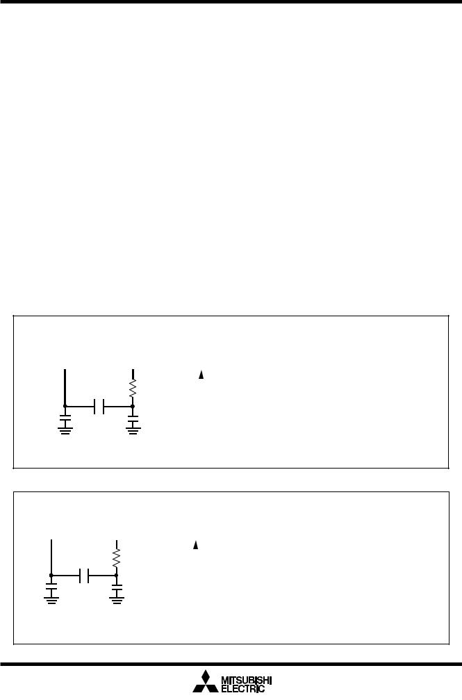
Underdevelopment
Clock Generating Circuit
Mitsubishi microcomputers
M30201 Group
SINGLE-CHIP 16-BIT CMOS MICROCOMPUTER
Clock Generating Circuit
The clock generating circuit contains two oscillator circuits that supply the operating clock sources to the
CPU and internal peripheral units.
Table 1.3. Main clock and sub-clock generating circuits
|
Main clock generating circuit |
Sub clock generating circuit |
|
|
|
Use of clock |
• CPU’s operating clock source |
• CPU’s operating clock source |
|
• Internal peripheral units’ |
• Timer A/B/X’s count clock |
|
operating clock source |
source |
|
|
|
Usable oscillator |
Ceramic or crystal oscillator |
Crystal oscillator |
|
|
|
Pins to connect oscillator |
XIN, XOUT |
XCIN, XCOUT |
|
|
|
Oscillation stop/restart function |
Available |
Available |
|
|
|
Oscillator status immediately after reset |
Oscillating |
Stopped |
|
|
|
Other |
Externally derived clock can be input |
|
|
|
|
Example of oscillator circuit
Figure 1.15 shows some examples of the main clock circuit, one using an oscillator connected to the circuit, and the other one using an externally derived clock for input. Figure 1.16 shows some examples of subclock circuits, one using an oscillator connected to the circuit, and the other one using an externally derived clock for input. Circuit constants in Figures 15 and 16 vary with each oscillator used. Use the values recommended by the manufacturer of your oscillator.
|
|
M30201 |
|
|
|
|
|
|
|
|
M30201 |
|
|
|||||||||
(Built-in feedback resistor) |
|
|
(Built-in feedback resistor) |
|
|
|||||||||||||||||
XIN |
XOUT |
|
|
XIN |
|
|
|
|
XOUT |
|
|
|||||||||||
|
|
|
|
|
|
|
|
|
|
|
|
|
|
|
|
|
|
|
|
|
|
|
|
|
|
|
|
|
|
(Note) |
|
|
|
|
|
|
|
|
Open |
|
|
||||
|
|
|
|
|
|
|
|
|
|
|
|
|
|
|
|
|
|
|
|
|
||
|
|
|
|
|
|
|
Rd |
|
|
|
|
|
|
|
|
|
|
|
|
|
|
|
|
|
|
|
|
|
|
|
|
|
|
|
|
|
|
|
|
|
|
||||
|
|
|
|
|
|
|
|
|
|
|
|
|
|
|
|
|
|
|
|
|
|
|
|
|
|
|
|
|
|
|
|
|
Externally derived clock |
|
|
||||||||||
|
|
|
|
|
|
|
|
|
|
|
|
|||||||||||
|
|
|
|
|
|
|
|
|
Vcc |
|
|
|
|
|
|
|
|
|
|
|
||
|
|
CIN |
|
|
COUT |
|
|
|
|
|
|
|
|
|
|
|
||||||
|
|
|
|
|
|
|
|
|
|
|
|
|
|
|
||||||||
|
|
|
|
Vss |
|
|
|
|
|
|
|
|
|
|
|
|
||||||
|
|
|
|
|
|
|
|
|
|
|
|
|
|
|
|
|
|
|
|
|
||
|
|
|
|
|
|
|
|
|
|
|
|
|
|
|
|
|
|
|
|
|
||
Note: Insert a damping resistor if required. The resistance will vary depending on the oscillator and the oscillation drive capacity setting. Use the value recommended by the maker of the oscillator.
When the oscillation drive capacity is set to low, check that oscillation is stable. Also, if the oscillator manufacturer's data sheet specifies that a feedback resistor be added external to the chip, insert a feedback resistor between XIN and XOUT following the instruction.
Figure 1.15. Examples of main clock
M30201 |
|
|
|
|
|
|
M30201 |
|
|
|||||||||
(Built-in feedback resistor) |
|
|
(Built-in feedback resistor) |
|
|
|||||||||||||
XCIN |
XCOUT |
|
|
XCIN |
|
|
|
XCOUT |
|
|
||||||||
|
|
|
|
|
|
|
|
|
|
|
|
|
|
|
|
|
|
|
|
|
|
(Note) |
|
|
|
|
|
|
|
|
Open |
|
|
||||
|
|
|
|
|
|
|
|
|
|
|
|
|
|
|
|
|
||
|
|
|
RCd |
|
|
|
|
|
|
|
|
|
|
|
|
|
|
|
|
|
|
|
|
|
|
|
|
|
|
|
|
|
|
|
|
||
CCIN |
|
|
CCOUT |
|
Externally derived clock |
|
|
|||||||||||
|
|
|
|
|
||||||||||||||
|
|
Vcc |
|
|
|
|
|
|
|
|
|
|
|
|||||
|
|
|
|
|
|
|
|
|
|
|
|
|
||||||
|
|
|
|
|
|
|
|
|
|
|
|
|
|
|
|
|||
|
|
|
|
|
Vss |
|
|
|
|
|
|
|
|
|
|
|
|
|
|
|
|
|
|
|
|
|
|
|
|
|
|
|
|
|
|
||
Note: Insert a damping resistor if required. The resistance will vary depending on the oscillator and the oscillation drive capacity setting. Use the value recommended by the maker of the oscillator.
When the oscillation drive capacity is set to low, check that oscillation is stable. Also,
if the oscillator manufacturer's data sheet specifies that a feedback resistor be added external to the chip, insert a feedback resistor between XCIN and XCOUT following the instruction.
Figure 1.16. Examples of sub-clock
18

Underdevelopment
Clock Generating Circuit
Mitsubishi microcomputers
M30201 Group
SINGLE-CHIP 16-BIT CMOS MICROCOMPUTER
Clock Control
Figure 1.17 shows the block diagram of the clock generating circuit.
|
|
XCIN |
XCOUT |
|
fC32 |
|
|
|
|
|
|
|
1/32 |
|
|
|
|
|
|
|
|
|
f1 |
|
|
|
|
|
CM04 |
|
|
|
|
|
|
|
|
|
|
|
|
|
|
|
|
|
|
|
|
fAD |
|
|
|
|
|
|
|
|
fC |
|
|
|
|
|
|
Sub clock |
|
|
|
f8 |
|
|
|
|
|
|
|
|
|
|
CM10 “1” |
S |
Q |
|
|
|
|
f32 |
|
Write signal |
|
|
|
|
|
|
||
|
XIN |
XOUT |
|
|
|
|
|
|
|
|
|
b |
c |
|
|
||
|
R |
|
|
|
d CM07=0 |
|
||
|
|
|
|
a |
|
|
||
|
|
|
|
|
|
|
||
RESET |
|
|
|
|
Divider |
|
|
|
|
|
|
|
|
|
|
|
|
Software reset |
|
Main clock |
|
|
|
fC |
BCLK |
|
|
|
|
|
|
||||
|
|
CM05 |
CM02 |
|
|
|
CM07=1 |
|
|
|
|
|
|
|
|||
Interrupt request level judgment output
S Q
WAIT instruction  R
R
CM0i : Bit i at address 000616 CM1i : Bit i at address 000716 WDCi : Bit i at address 000F16
a
|
|
|
b |
c |
1/2 |
1/2 |
1/2 |
1/2 |
1/2 |
|
|
|
|
CM06=0 |
|
|
|
|
CM17,CM16=11 |
|
|
|
CM06=1 |
|
|
|
CM06=0 |
|
|
|
|
CM17,CM16=10 |
d |
|
|
|
|
|
|
|
CM06=0 |
|
|
|
|
CM17,CM16=01 |
|
|
|
CM06=0 |
|
|
|
|
CM17,CM16=00 |
|
|
|
|
Details of divider
Figure 1.17. Clock generating circuit
19

Underdevelopment
Clock Generating Circuit
Mitsubishi microcomputers
M30201 Group
SINGLE-CHIP 16-BIT CMOS MICROCOMPUTER
The following paragraphs describes the clocks generated by the clock generating circuit.
(1) Main clock
The main clock is generated by the main clock oscillation circuit. After a reset, the clock is divided by 8 to BCLK. The clock can be stopped using the main clock stop bit (bit 5 at address 000616). Stopping the clock, after switching the operating clock source of CPU to the sub-clock, reduces the power dissipation. After the oscillation of the main clock oscillation circuit has stabilized, the drive capacity of the main clock oscillation circuit can be reduced using the XIN-XOUT drive capacity select bit (bit 5 at address 000716). Reducing the drive capacity of the main clock oscillation circuit reduces the power dissipation. This bit changes to “1” when shifting from high-speed/medium-speed mode to stop mode and at a reset. When shifting from low-speed/low power dissipation mode to stop mode, the value before stop mode is retained.
(2) Sub-clock
The sub-clock is generated by the sub-clock oscillation circuit. No sub-clock is generated after a reset. After oscillation is started using the port Xc select bit (bit 4 at address 000616), the sub-clock can be selected as BCLK by using the system clock select bit (bit 7 at address 000616). However, be sure that the sub-clock oscillation has fully stabilized before switching.
After the oscillation of the sub-clock oscillation circuit has stabilized, the drive capacity of the sub-clock oscillation circuit can be reduced using the XCIN-XCOUT drive capacity select bit (bit 3 at address 000616). Reducing the drive capacity of the sub-clock oscillation circuit reduces the power dissipation. This bit changes to “1” when shifting to stop mode and at a reset.
(3) BCLK
The BCLK is the clock that drives the CPU, and is fc or the clock is derived by dividing the main clock by 1, 2, 4, 8, or 16. The BCLK is derived by dividing the main clock by 8 after a reset.
The main clock division select bit 0(bit 6 at address 000616) changes to “1” when shifting from high- speed/medium-speed to stop mode and at reset. When shifting from low-speed/low power dissipation mode to stop mode, the value before stop mode is retained.
(4) Peripheral function clock (f1, f8, f32, fAD)
The clock for the peripheral devices is derived from the main clock or by dividing it by 8 or 32. The peripheral function clock is stopped by stopping the main clock or by setting the WAIT peripheral function clock stop bit (bit 2 at 000616) to “1” and then executing a WAIT instruction.
(5) fC32
This clock is derived by dividing the sub-clock by 32. It is used for the timer A, timer B and timer X counts.
(6) fC
This clock has the same frequency as the sub-clock. It is used for BCLK and for the watchdog timer.
20
Underdevelopment
Clock Generating Circuit
Mitsubishi microcomputers
M30201 Group
SINGLE-CHIP 16-BIT CMOS MICROCOMPUTER
Figure 1.18 shows the system clock control registers 0 and 1.
System clock control register 0 (Note 1)
b7 b6 b5 b4 b3 b2 b1 b0
|
|
|
|
|
|
|
|
Symbol |
Address |
When reset |
|
|
|
|
|
|
|
|
|
CM0 |
000616 |
4816 |
|
|
|
|
|
|
|
|
|
|
|
|
|
|
|
|
|
|
|
|
|
Bit symbol |
Bit name |
Function |
R W |
|
|
|
|
|
|
|
|
CM00 |
Clock output function |
b1 b0 |
|
|
|
|
|
|
|
|
|
0 0 : I/O port P54 |
|
||
|
|
|
|
|
|
|
|
|
select bit |
|
|
|
|
|
|
|
|
|
|
|
0 1 : fC output |
|
|
|
|
|
|
|
|
|
|
|
|
|
|
|
|
|
|
|
|
|
|
CM01 |
|
1 0 : f8 output |
|
|
|
|
|
|
|
|
|
|
|
1 1 : Clock divide counter output |
|
|
|
|
|
|
|
|
|
CM02 |
WAIT peripheral function 0 : Do not stop peripheral function clock in wait mode |
|
|
|
|
|
|
|
|
|
|
clock stop bit |
1 : Stop peripheral function clock in wait mode (Note 8) |
|
|
|
|
|
|
|
|
|
|
|
|
||
|
|
|
|
|
|
|
|
CM03 |
XCIN-XCOUT drive capacity |
0 : LOW |
|
|
|
|
|
|
|
|
|
|
|||
|
|
|
|
|
|
|
|
select bit (Note 2) |
1 : HIGH |
|
|
|
|
|
|
|
|
|
|
|
|
||
|
|
|
|
|
|
|
|
CM04 |
Port XC select bit |
0 : I/O port |
|
|
|
|
|
|
|
|
|
|
|||
|
|
|
|
|
|
|
|
|
1 : XCIN-XCOUT generation |
|
|
|
|
|
|
|
|
|
|
|
|
|
|
|
|
|
|
|
|
|
|
CM05 |
Main clock (XIN-XOUT) |
0 : On |
|
|
|
|
|
|
|
|
|
|
|||
|
|
|
|
|
|
|
|
|
stop bit (Note 3,4,5) |
1 : Off |
|
|
|
|
|
|
|
|
|
CM06 |
Main clock division select |
0 : CM16 and CM17 valid |
|
|
|
|
|
|
|
|
|
|
|||
|
|
|
|
|
|
|
|
bit 0 (Note 7) |
1 : Division by 8 mode |
|
|
|
|
|
|
|
|
|
|
|
|
||
|
|
|
|
|
|
|
|
CM07 |
System clock select bit |
0 : XIN, XOUT |
|
|
|
|
|
|
|
|
|
|
|||
|
|
|
|
|
|
|
|
(Note 6) |
1 : XCIN, XCOUT |
|
|
|
|
|
|
|
|
|
|
|
|
||
|
|
|
|
|
|
|
|
|
|
|
|
Note 1: Set bit 0 of the protect register (address 000A16) to “1” before writing to this register. Note 2: Changes to “1” when shifting to stop mode and at a reset.
Note 3: This bit is used to stop the main clock when placing the device in a low-power mode. If you want to operate with XIN after exiting from the stop mode, set this bit to “0”. When operating with a self-excited oscillator, set the system clock select bit (CM07) to “1” before setting this bit to “1”.
Note 4: When inputting external clock, only clock oscillation buffer is stopped and clock input is acceptable.
Note 5: If this bit is set to “1”, XOUT turns “H”. The built-in feedback resistor remains being connected, so XIN turns pulled up to XOUT (“H”) via the feedback resistor.
Note 6: Set port Xc select bit (CM04) to “1” and stabilize the sub-clock oscillating before setting to this bit from “0” to “1”.
Do not write to both bits at the same time. And also, set the main clock stop bit (CM05) to “0” and stabilize the main clock oscillating before setting this bit from “1” to “0”.
Note 7: This bit changes to “1” when shifting from high-speed/medium-speed mode to stop mode and at a reset. When shifting from low-speed/low power dissipation mode to stop mode, the value before stop mode is retained.
Note 8: fC32 is not included.
System clock control register 1 (Note 1)
b7 |
b6 |
b5 |
b4 |
b3 |
b2 |
b1 |
b0 |
|
|
|
|
|
|
|
0 |
|
0 |
0 |
|
Symbol |
Address |
When reset |
|
|
|
|
|
|
CM1 |
000716 |
2016 |
|
|||
|
|
|
|
|
|
|
|
|
|||
|
|
|
|
|
|
|
|
|
|||
|
|
|
|
|
|
|
|
|
|
|
|
|
|
|
|
|
|
|
|
Bit symbol |
Bit name |
Function |
R W |
|
|
|
|
|
|
|
|
|
|
|
|
|
|
|
|
|
|
|
|
CM10 |
All clock stop control bit |
0 : Clock on |
|
|
|
|
|
|
|
|
|
|
(Note 4) |
1 : All clocks off (stop mode) |
|
|
|
|
|
|
|
|
|
Reserved bit |
Always set to “0” |
|
|
|
|
|
|
|
|
|
|
Reserved bit |
Always set to “0” |
|
|
|
|
|
|
|
|
|
|
Reserved bit |
Always set to “0” |
|
|
|
|
|
|
|
|
|
|
Reserved bit |
Always set to “0” |
|
|
|
|
|
|
|
|
|
|
CM15 |
XIN-XOUT drive capacity |
0 : LOW |
|
|
|
|
|
|
|
|
|
|
|||
|
|
|
|
|
|
|
|
select bit (Note 2) |
1 : HIGH |
|
|
|
|
|
|
|
|
|
|
|
|
||
|
|
|
|
|
|
|
|
|
|
b7 b6 |
|
|
|
|
|
|
|
|
|
|
|
|
|
|
|
|
|
|
|
|
|
CM16 |
Main clock division |
0 0 : No division mode |
|
|
|
|
|
|
|
|
|
|
select bit 1 (Note 3) |
0 1 : Division by 2 mode |
|
|
|
|
|
|
|
|
|
CM17 |
|
1 0 : Division by 4 mode |
|
|
|
|
|
|
|
|
|
|
1 1 : Division by 16 mode |
|
|
|
|
|
|
|
|
|
|
|
|
|
|
|
|
|
|
|
|
|
|
|
|
|
|
Note 1: Set bit 0 of the protect register (address 000A16) to “1” before writing to this register.
Note 2: This bit changes to “1” when shifting from high-speed/medium-speed mode to stop mode and at a reset. When shifting from low-speed/low power dissipation mode to stop mode, the value before stop mode is retained.
Note 3: Can be selected when bit 6 of the system clock control register 0 (address 000616) is “0”. If “1”, division mode isedfix at 8. Note 4: If this bit is set to “1”, XOUT turns “H”, and the built-in feedback resistor is cut off. XCIN and XCOUT turn high-impedance state.
Figure 1.18. Clock control registers 0 and 1
21
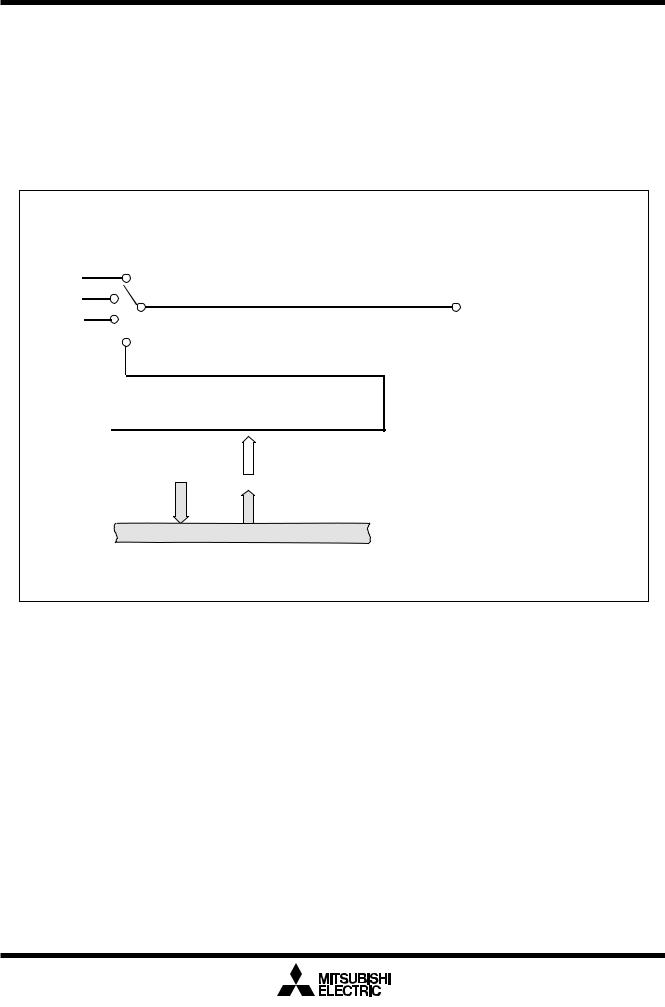
Underdevelopment
Clock Generating Circuit
Mitsubishi microcomputers
M30201 Group
SINGLE-CHIP 16-BIT CMOS MICROCOMPUTER
Clock Output
The clock output function select bit allows you to choose the clock from f8, fc, or a divide-by-n clock that is output from the P54/CKOUT pin. The clock divide counter is an 8-bit counter whose count source is f32, and its divide ratio can be set in the range of 0016 to FF16. Figure 1.19 shows a block diagram of clock output.
Clock source selection
P54
f8
P54/CKOUT
fC
|
|
|
|
1/2 |
|
|
|
|
|
f32 |
|
|
|
|
|
|
|
|
|
|
|
|
|
|
|
|
|||
|
|
Clock divided couter (8) |
|
|
|
|
|||
|
|
|
|
Division n+1 n=0016 to FF16 |
Example: |
|
|||
|
|
|
|
|
|
|
|
||
|
|
|
Reload register (8) |
Address 038E16 |
When f(XIN)=10MHz |
||||
|
|
|
n=0716 |
: |
approx. 16.5kHz |
||||
|
|
|
|
|
|
|
|||
|
|
|
|
|
|
|
|||
|
|
|
|
Low-order 8 bits |
|
n=2616 |
: |
approx. 4.0kHz |
|
|
|
|
|
|
|
|
n=4D16 |
: |
approx. 2.0kHz |
|
|
|
|
|
|
n=9B16 |
: |
approx. 1.0kHz |
|
|
|
|
Data bus low-order bits |
|
|||||
Figure 1.19. Block diagram of clock output
22

Underdevelopment
ClockWait ModeGenerating Circuit
Mitsubishi microcomputers
M30201 Group
SINGLE-CHIP 16-BIT CMOS MICROCOMPUTER
Stop Mode
Writing “1” to the all-clock stop control bit (bit 0 at address 000716) stops all oscillation and the microcomputer enters stop mode. In stop mode, the content of the internal RAM is retained provided that VCC remains above 2V.
Because the oscillation of BCLK, f1 to f32, fc, fc32, and fAD stops in stop mode, peripheral functions such as the A-D converter and watchdog timer do not function. However, timer A, timer B and timer X operate provided that the event counter mode is set to an external pulse, and UART0 functions provided an external clock is selected. Table 1.4 shows the status of the ports in stop mode.
Stop mode is cancelled by a hardware reset or an interrupt. If an interrupt is to be used to cancel stop mode, that interrupt must first have been enabled. If returning by an interrupt, that interrupt routine is executed. When shifting from high-speed/medium-speed mode to stop mode and at a reset, the main clock division select bit 0 (bit 6 at address 000616) is set to “1”. When shifting from low-speed/low power dissipation mode to stop mode, the value before stop mode is retained.
Table 1.4. Port status during stop mode
|
Pin |
States |
|
|
|
Port |
|
Retains status before stop mode |
|
|
|
CLKOUT |
When fC selected |
“H” |
|
|
|
|
When f8, clock devided |
Retains status before stop mode |
|
counter output selected |
|
|
|
|
Wait Mode
When a WAIT instruction is executed, BCLK stops and the microcomputer enters the wait mode. In this mode, oscillation continues but BCLK and watchdog timer stop. Writing “1” to the WAIT peripheral function clock stop bit and executing a WAIT instruction stops the clock being supplied to the internal peripheral functions, allowing power dissipation to be reduced. Table 1.5 shows the status of the ports in wait mode. Wait mode is cancelled by a hardware reset or interrupt. If an interrupt is used to cancel wait mode, the microcomputer restarts from the interrupt routine using as BCLK, the clock that had been selected when the WAIT instruction was executed.
Table 1.5. Port status during wait mode
|
Pin |
States |
|
|
|
Port |
|
Retains status before wait mode |
|
|
|
CLKOUT |
When fC selected |
Does not stop |
|
|
|
|
When f8, clock devided |
Does not stop when the WAIT |
|
counter output selected |
peripheral function clock stop bit is “0”. |
|
|
When the WAIT peripheral function |
|
|
clock stop bit is “1”,the status immedi- |
|
|
ately prior to entering wait mode is |
|
|
maintained. |
|
|
|
23

Underdevelopment
ClockStatusGeneratingTransition ofCircuitBCLK
Mitsubishi microcomputers
M30201 Group
SINGLE-CHIP 16-BIT CMOS MICROCOMPUTER
Status Transition of BCLK
Power dissipation can be reduced and low-voltage operation achieved by changing the count source for BCLK. Table 1.6 shows the operating modes corresponding to the settings of system clock control registers 0 and 1.
When reset, the device starts in division by 8 mode. The main clock division select bit 0(bit 6 at address 000616) changes to “1” when shifting from high-speed/medium-speed to stop mode and at a reset. When shifting from low-speed/low power dissipation mode to stop mode, the value before stop mode is retained. The following shows the operational modes of BCLK.
(1) Division by 2 mode
The main clock is divided by 2 to obtain the BCLK.
(2) Division by 4 mode
The main clock is divided by 4 to obtain the BCLK.
(3) Division by 8 mode
The main clock is divided by 8 to obtain the BCLK. When reset, the device starts operating from this mode. Before the user can go from this mode to no division mode, division by 2 mode, or division by 4 mode, the main clock must be oscillating stably. When going to low-speed or lower power consumption mode, make sure the sub-clock is oscillating stably.
(4) Division by 16 mode
The main clock is divided by 16 to obtain the BCLK.
(5) No-division mode
The main clock is divided by 1 to obtain the BCLK.
(6) Low-speed mode
fC is used as BCLK. Note that oscillation of both the main and sub-clocks must have stabilized before transferring from this mode to another or vice versa. At least 2 to 3 seconds are required after the subclock starts. Therefore, the program must be written to wait until this clock has stabilized immediately after powering up and after stop mode is cancelled.
(7) Low power dissipation mode
fC is the BCLK and the main clock is stopped.
Note : Before the count source for BCLK can be changed from XIN to XCIN or vice versa, the clock to which the count source is going to be switched must be oscillating stably. Allow a wait time in software for the oscillation to stabilize before switching over the clock.
Table 1.6. Operating modes dictated by settings of system clock control registers 0 and 1
|
CM17 |
CM16 |
CM07 |
CM06 |
CM05 |
CM04 |
Operating mode of BCLK |
|
|
|
|
|
|
|
|
|
|
|
0 |
1 |
0 |
0 |
0 |
Invalid |
Division by 2 mode |
|
|
|
|
|
|
|
|
|
|
|
1 |
0 |
0 |
0 |
0 |
Invalid |
Division by 4 mode |
|
|
|
|
|
|
|
|
|
|
|
Invalid |
Invalid |
0 |
1 |
0 |
Invalid |
Division by 8 mode |
|
|
|
|
|
|
|
|
|
|
|
1 |
1 |
0 |
0 |
0 |
Invalid |
Division by 16 mode |
|
|
|
|
|
|
|
|
|
|
|
0 |
0 |
0 |
0 |
0 |
Invalid |
No-division mode |
|
|
|
|
|
|
|
|
|
|
|
Invalid |
Invalid |
1 |
Invalid |
0 |
1 |
Low-speed mode |
|
|
|
|
|
|
|
|
|
|
|
Invalid |
Invalid |
1 |
Invalid |
1 |
1 |
Low power dissipation mode |
|
|
|
|
|
|
|
|
|
|
|
|
|
|
|
|
|
|
|
|
|
|
|
|
|
|
|
|
24

Underdevelopment
PowerClock GeneratingSaving Circuit
Mitsubishi microcomputers
M30201 Group
SINGLE-CHIP 16-BIT CMOS MICROCOMPUTER
Power Saving
There are three power save modes.
(1)Normal operating mode
•High-speed mode
In this mode, one main clock cycle forms BCLK. The CPU operates on the BCLK. The peripheral functions operate on the clocks specified for each respective function.
•Medium-speed mode
In this mode, the main clock is divided into 2, 4, 8, or 16 to form BCLK. The CPU operates on the BCLK. The peripheral functions operated on the clocks specified for each respective function.
•Low-speed mode
In this mode, fc forms BCLK. The CPU operates on the fc clock. fc is the clock supplied by the subclock. The peripheral functions operate on the clocks specified for each respective function.
•Low power-dissipation mode
This mode is selected when the main clock is stopped from low-speed mode. The CPU operates on the fc clock. fc is the clock supplied by the subclock. Only the peripheral functions for which the subclock was selected as the count source continue to run.
(2)Wait mode
CPU operation is halted in this mode. The oscillator continues to run.
(3) Stop mode
All oscillators stop in this mode. The CPU and internal peripheral functions all stop. Of all 3 power saving modes, power savings are greatest in this mode.
Figure 1.20 shows the transition between each of the three modes, (1), (2), and (3).
25
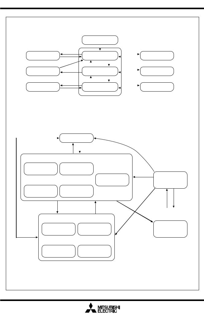
Underdevelopment
PowerClock GeneratingSaving Circuit
Mitsubishi microcomputers
M30201 Group
SINGLE-CHIP 16-BIT CMOS MICROCOMPUTER
Transition of stop mode, wait mode
Reset
All oscillators stopped
CM10 = “1”
Stop mode
Interrupt
All oscillators stopped Interrupt
Stop mode |
CM10 = “1” |
All oscillators stopped
CM10 = “1”
Stop mode
Interrupt
Transition of normal mode
|
|
|
|
|
|
|
WAIT |
|
CPU operation stopped |
|
|
|
|
|
|
||||
Medium-speed mode |
|
instruction |
|
Wait mode |
|||||
|
|
|
|||||||
|
(divided-by-8 mode) |
|
|
|
|||||
|
|
Interrupt |
|
||||||
|
|
|
|
||||||
|
|
|
|
|
|
|
|
|
|
|
|
|
|
|
|
|
WAIT |
|
CPU operation stopped |
|
|
|
|
|
|
||||
High-speed/medium- |
|
instruction |
|
Wait mode |
|||||
|
|
|
|||||||
|
|
speed mode |
|
|
|
||||
|
|
|
Interrupt |
|
|||||
|
|
|
|
|
|||||
|
|
|
|
|
|
|
|
|
|
|
|
|
|
|
|
|
WAIT |
|
CPU operation stopped |
|
|
|
|
|
|
||||
Low-speed/low power |
|
instruction |
|
Wait mode |
|||||
|
|
|
|||||||
|
dissipation mode |
|
Interrupt |
|
|
||||
|
|
|
|
|
|
|
|
|
|
|
|
|
|
|
|
||||
|
Normal mode |
|
|
|
|
|
|||
(Refer to the following for the transition of normal mode.)
Main clock is oscillating Sub clock is stopped
Medium-speed mode (divided-by-8 mode)
CM06 = “1” |
BCLK : f(XIN)/8 |
||
|
CM07 = “0” CM06 = “1” |
||
Main clock is oscillating |
CM04 = “0” |
|
CM04 = “1” |
|
|||
|
(Notes 1, 3) |
||
Sub clock is oscillating |
|
|
|
High-speed mode |
Medium-speed mode |
||
(divided-by-2 mode) |
|||
BCLK : f(XIN) |
BCLK : f(XIN)/2 |
CM07 = “0” CM06 = “0” |
CM07 = “0” CM06 = “0” |
CM17 = “0” CM16 = “0” |
CM17 = “0” CM16 = “1” |
Medium-speed mode |
Medium-speed mode |
(divided-by-4 mode) |
(divided-by-16 mode) |
BCLK : f(XIN)/4 |
BCLK : f(XIN)/16 |
CM07 = “0” CM06 = “0” |
CM07 = “0” CM06 = “0” |
CM17 = “1” CM16 = “0” |
CM17 = “1” CM16 = “1” |
CM04 = “0” Main clock is oscillating
Sub clock is stopped
Medium-speed mode (divided-by-8 mode)
BCLK : f(XIN)/8
CM07 = “0”
CM06 = “1”
CM04 = “1”
|
Medium-speed mode |
High-speed mode |
(divided-by-2 mode) |
CM07 = “0” (Note 1)
CM06 = “1”
CM04 = “0”
Main clock is oscillating Sub clock is oscillating
Low-speed mode
CM07 = “0”
(Note 1, 3)
BCLK : f(XCIN)
 CM07 = “1” CM07 = “1”
(Note 2)
CM05 = “0” |
CM05 = “1” |
Main clock is stopped
Sub clock is oscillating
Low power dissipation mode
CM06 = “0” (Notes 1,3)
BCLK : f(XIN) |
BCLK : f(XIN)/2 |
CM07 = “0” CM06 = “0” |
CM07 = “0” CM06 = “0” |
CM17 = “0” CM16 = “0” |
CM17 = “0” CM16 = “1” |
Medium-speed mode |
Medium-speed mode |
(divided-by-4 mode) |
(divided-by-16 mode) |
BCLK : f(XIN)/4 |
BCLK : f(XIN)/16 |
CM07 = “0” CM06 = “0” |
CM07 = “0” CM06 = “0” |
CM17 = “1” CM16 = “0” |
CM17 = “1” CM16 = “1” |
CM07 = “1” (Note 2)
CM05 = “1” |
BCLK : f(XCIN) |
|
|
|
CM07 = “1” |
CM07 = “0” (Note 1) |
|
CM06 = “0” (Note 3) |
|
CM04 = “1” |
|
Note 1: Switch clock after oscillation of main clock is sufficiently stable.
Note 2: Switch clock after oscillation of sub clock is sufficiently stable.
Note 3: Change CM06 after changing CM17 and CM16.
Note 4: Transit in accordance with arrow.
Figure 1.20. Clock transition
26
Underdevelopment
PrClocktectionGenerating Circuit
Mitsubishi microcomputers
M30201 Group
SINGLE-CHIP 16-BIT CMOS MICROCOMPUTER
Protection
The protection function is provided so that the values in important registers cannot be changed in the event that the program runs out of control. Figure 1.21 shows the protect register. The values in the processor mode register 0 (address 000416), processor mode register 1 (address 000516), system clock control register 0 (address 000616), system clock control register 1 (address 000716) and port P4 direction register (address 03EA16) can only be changed when the respective bit in the protect register is set to “1”. Therefore, important outputs can be allocated to port P4.
If, after “1” (write-enabled) has been written to the port P4 direction register write-enable bit (bit 2 at address 000A16), a value is written to any address, the bit automatically reverts to “0” (write-inhibited). However, the system clock control registers 0 and 1 write-enable bit (bit 0 at 000A16) and processor mode register 0 and 1 write-enable bit (bit 1 at 000A16) do not automatically return to “0” after a value has been written to an address. The program must therefore be written to return these bits to “0”.
Protect register
b7 b6 b5 b4 b3 b2 b1 b0
|
|
|
|
|
|
|
|
Symbol |
Address |
When reset |
|
|
|
|
|
|
|
|
PRCR |
000A16 |
XXXXX0002 |
Bit symbol |
Bit name |
Enables writing to system clock PRC0 control registers 0 and 1 (addresses
000616 and 000716)
Enables writing to processor mode PRC1 registers 0 and 1 (addresses 000416
and 000516)
Function |
R W |
|
|
0 : Write-inhibited
1 : Write-enabled
0 : Write-inhibited
1 : Write-enabled
PRC2 |
Enables writing to port P4 direction |
0 |
: Write-inhibited |
|
register (address 03EA16) (Note) |
1 |
: Write-enabled |
||
|
Nothing is assigned.
These bits can neither be set nor reset. When read, their contents are indeterminate.
Note: Writing a value to an address after “1” is written to this bit returns the bit
to “0” . Other bits do not automatically return to “0” and they must therefore be reset by the program
Figure 1.21. Protect register
27

Underdevelopment
Interrupts
Overview of Interrupt
Type of Interrupts
Figure 1.22 lists the types of interrupts.
Mitsubishi microcomputers
M30201 Group
SINGLE-CHIP 16-BIT CMOS MICROCOMPUTER
|
|
|
|
|
|
|
|
|
Undefined instruction (UND instruction) |
|
|
Software |
|
|
|
|
|
|
Overflow (INTO instruction) |
|
|
|
|
|
|
|
|
BRK instruction |
|
|
|
|
|
|
|
||||
|
|
|
|
|
|
|
|
INT instruction |
|
|
|
|
|
|
|
|
|
||
|
|
|
|
|
|
|
|
|
|
|
|
|
|
|
|
|
|
|
|
|
|
|
|
|
|
|
|
|
|
Interrupt |
|
|
|
|
|
|
|
|
|
|
|
|
|
|
|
|
|
Reset |
|
|
|
|
|
|
|
|
|||
|
|
|
|
|
|
|
|
________ |
|
|
|
|
|
|
|
|
|
DBC |
|
|
|
|
|
|
|
Special |
|
Watchdog timer |
|
|
|
|
|
|
|
||||
|
|
|
|
|
|
|
Single step |
||
|
|
|
|
|
|
|
|
||
|
|
Hardware |
|
|
|
Address matched |
|||
|
|
|
|
|
|
||||
|
|
|
|
||||||
|
|
|
|
|
|
|
|
||
|
|
|
|
|
|
|
|
|
|
|
|
|
|
|
|
Peripheral I/O*1 |
|
|
|
*1 Peripheral I/O interrupts are generated by the peripheral functions built into the microcomputer system.
Figure 1.22. Classification of interrupts
• Maskable interrupt |
: An interrupt which can be enabled (disabled) by the interrupt enable flag (I |
|
flag) or whose interrupt priority can be changed by priority level. |
• Non-maskable interrupt |
: An interrupt which cannot be enabled (disabled) by the interrupt enable flag |
|
(I flag) or whose interrupt priority cannot be changed by priority level. |
28

Underdevelopment
Interrupts
Mitsubishi microcomputers
M30201 Group
SINGLE-CHIP 16-BIT CMOS MICROCOMPUTER
Software Interrupts
A software interrupt occurs when executing certain instructions. Software interrupts are non-maskable interrupts.
• Undefined instruction interrupt
An undefined instruction interrupt occurs when executing the UND instruction.
• Overflow interrupt
An overflow interrupt occurs when executing the INTO instruction with the overflow flag (O flag) set to “1”. The following are instructions whose O flag changes by arithmetic:
ABS, ADC, ADCF, ADD, CMP, DIV, DIVU, DIVX, NEG, RMPA, SBB, SHA, SUB
• BRK interrupt
A BRK interrupt occurs when executing the BRK instruction.
• INT interrupt
An INT interrupt occurs when assigning one of software interrupt numbers 0 through 63 and executing the INT instruction. Software interrupt numbers 0 through 31 are assigned to peripheral I/O interrupts, so executing the INT instruction allows executing the same interrupt routine that a peripheral I/O interrupt does.
The stack pointer (SP) used for the INT interrupt is dependent on which software interrupt number is involved.
So far as software interrupt numbers 0 through 31 are concerned, the microcomputer saves the stack pointer assignment flag (U flag) when it accepts an interrupt request. If change the U flag to “0” and select the interrupt stack pointer (ISP), and then execute an interrupt sequence. When returning from the interrupt routine, the U flag is returned to the state it was before the acceptance of interrupt request. So far as software numbers 32 through 63 are concerned, the stack pointer does not make a shift.
29

Underdevelopment
Interrupts
Mitsubishi microcomputers
M30201 Group
SINGLE-CHIP 16-BIT CMOS MICROCOMPUTER
Hardware Interrupts
Hardware interrupts are classified into two types — special interrupts and peripheral I/O interrupts.
(1) Special interrupts
Special interrupts are non-maskable interrupts.
•Reset
Reset occurs if an “L” is input to the RESET pin.
•DBC interrupt
This interrupt is exclusively for the debugger, do not use it in other circumstances.
•Watchdog timer interrupt
Generated by the watchdog timer.
•Single-step interrupt
This interrupt is exclusively for the debugger, do not use it in other circumstances. With the debug flag (D flag) set to “1”, a single-step interrupt occurs after one instruction is executed.
•Address match interrupt
An address match interrupt occurs immediately before the instruction held in the address indicated by the address match interrupt register is executed with the address match interrupt enable bit set to “1”. If an address other than the first address of the instruction in the address match interrupt register is set, no address match interrupt occurs.
(2)Peripheral I/O interrupts
A peripheral I/O interrupt is generated by one of built-in peripheral functions. The interrupt vector table is the same as the one for software interrupt numbers 0 through 31 the INT instruction uses. Peripheral I/O interrupts are maskable interrupts.
• Key-input interrupt
___
A key-input interrupt occurs if an “L” is input to the KI pin.
•A-D conversion interrupt
This is an interrupt that the A-D converter generates.
•UART0 and UART1 transmission interrupt
These are interrupts that the serial I/O transmission generates.
•UART0 and UART1 reception interrupt
These are interrupts that the serial I/O reception generates.
•Timer A0 interrupt
This is an interrupts that timer A0 generates.
•Timer B0 and timer B2 interrupt
These are interrupts that timer B generates.
•Timer X0 to timer X2 interrupt
These are interrupts that timer X generates.
________ ________
• INT0 and INT1 interrupt
______ |
______ |
An INT interrupt occurs if either a rising edge or a falling edge is input to the INT pin.
30
 Loading...