


SG7905.2AIG
Microsemi Corporation SG7905.2AIG, SG7905.2AK, SG7905.2AR, SG7905.2T, SG7905AIG Datasheet
...
SG7900A/SG7900 SERIES
12/91 Rev 1.4 12/99 LINFINITY Microelectronics Inc.
Copyright 1999 11861 Western Avenue
∞ ∞
∞ ∞
∞ Garden Grove, CA 92841
1 (714) 898-8121
∞∞
∞∞
∞FAX: (714) 893-2570
NEGATIVE FIXED VOLTAGE REGULATOR
The SG7900A/SG7900 series of negative regulators offer self-contained,
fixed-voltage capability with up to 1.5A of load current. With a variety of
output voltages and four package options this regulator series is an
optimum complement to the SG7800A/SG7800, SG140 line of three
terminal regulators.
These units feature a unique band gap reference which allows the
SG7900A series to be specified with an output voltage tolerance of ±1.5%.
The SG7900A versions also offer much improved line regulation character-
istics.
All protective features of thermal shutdown, current limiting, and safe-area
control have been designed into these units and since these regulators
require only a single output capacitor (SG7900 series) or a capacitor and
5mA minimum load (SG120 series) for satisfactory performance, ease of
application is assured.
Although designed as fixed-voltage regulators, the output voltage can be
increased through the use of a simple voltage divider. The low quiescent
drain current of the device insures good regulation when this method is
used, especially for the SG120 series.
These devices are available in hermetically sealed TO-257, TO-3, TO-39
and LCC package.
DESCRIPTION
FEATURES
••
••
•
Output voltage set internally to
±±
±±
±1.5% on SG7900A
••
••
• Output current to 1.5A
••
••
• Excellent line and load regulation
••
••
• Foldback current limiting
••
••
• Thermal overload protection
••
••
• Voltages available: -5V, -12V, -15V
••
••
• Contact factory for other voltage options
••
••
• Available in surface mount package
HIGH RELIABILITY FEATURES
- SG7900A/SG7900
♦♦
♦♦
♦ Available to MIL-STD - 883
♦♦
♦♦
♦ MIL-M38510/11501BXA - JAN7905T
♦♦
♦♦
♦ MIL-M38510/11505BYA - JAN7905K
♦♦
♦♦
♦ MIL-M38510/11502BXA - JAN7912T
♦♦
♦♦
♦ MIL-M38510/11506BYA - JAN7912K
♦♦
♦♦
♦ MIL-M38510/11503BXA - JAN7915T
♦♦
♦♦
♦ MIL-M38510/11507BYA - JAN7915K
♦♦
♦♦
♦ LMI level "S" processing available
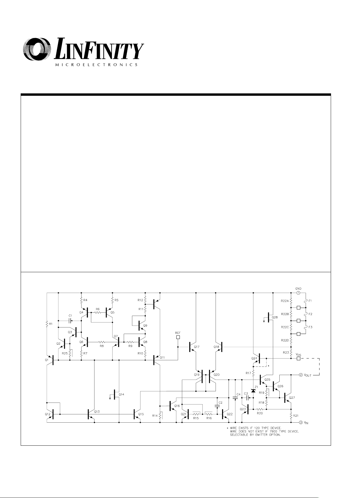
SCHEMATIC DIAGRAM
SG7900A/SG7900
**
**
For normal
operation the (V
OS
)
Sense Pin must be
externally
connected to the
load.
SG7900A/SG7900 SERIES
12/91 Rev 1.4 12/99 LINFINITY Microelectronics Inc.
Copyright 1999 11861 Western Avenue
∞ ∞
∞ ∞
∞ Garden Grove, CA 92841
2 (714) 898-8121
∞∞
∞∞
∞FAX: (714) 893-2570
ABSOLUTE MAXIMUM RATINGS (Note 1)
NEGATIVE REGULATOR
Device Input Voltage Differential
Output Voltage Input Voltage (Output shorted to ground)
-5V -35V 35V
-12V -35V 35V
-15V -40V 35V
150°C
-65°C to 150°C
300°C
Operating Junction Temperature
Hermetic (K, T, IG & L - Packages) ........................
Storage Temperature Range ..........................
Lead Temperature (Soldering, 10 Seconds) .................
Note 1. Values beyond which damage may occur.
THERMAL DATA
K Package:
Thermal Resistance-
Junction to Case, θ
JC
................. 3.0°C/W
Thermal Resistance-
Junction to Ambient, θ
JA
............... 35°C/W
T Package:
Thermal Resistance-Junction to Case, θ
JC
.................. 15°C/W
Thermal Resistance-Junction to Ambient, θ
JA
............ 120°C/W
IG Package:
Thermal Resistance-Junction to Case, θ
JC
................. 3.5°C/W
Thermal Resistance-Junction to Ambient, θ
JA
.............. 42°C/W
L Package:
Thermal Resistance-Junction to Case, θ
JC
.................. 35°C/W
Thermal Resistance-Junction to Ambient, θ
JA
............ 120°C/W
Note A. Junction Temperature Calculation: T
J
= T
A
+ (P
D
x θ
JA
).
Note B. The above numbers for θ
JC
are maximums for the limiting thermal
resistance of the package in a standard mounting configuration.
The θ
JA
numbers are meant to be guidelines for the thermal
performance of the device/pc-board system. All of the above
assume no ambient airflow.
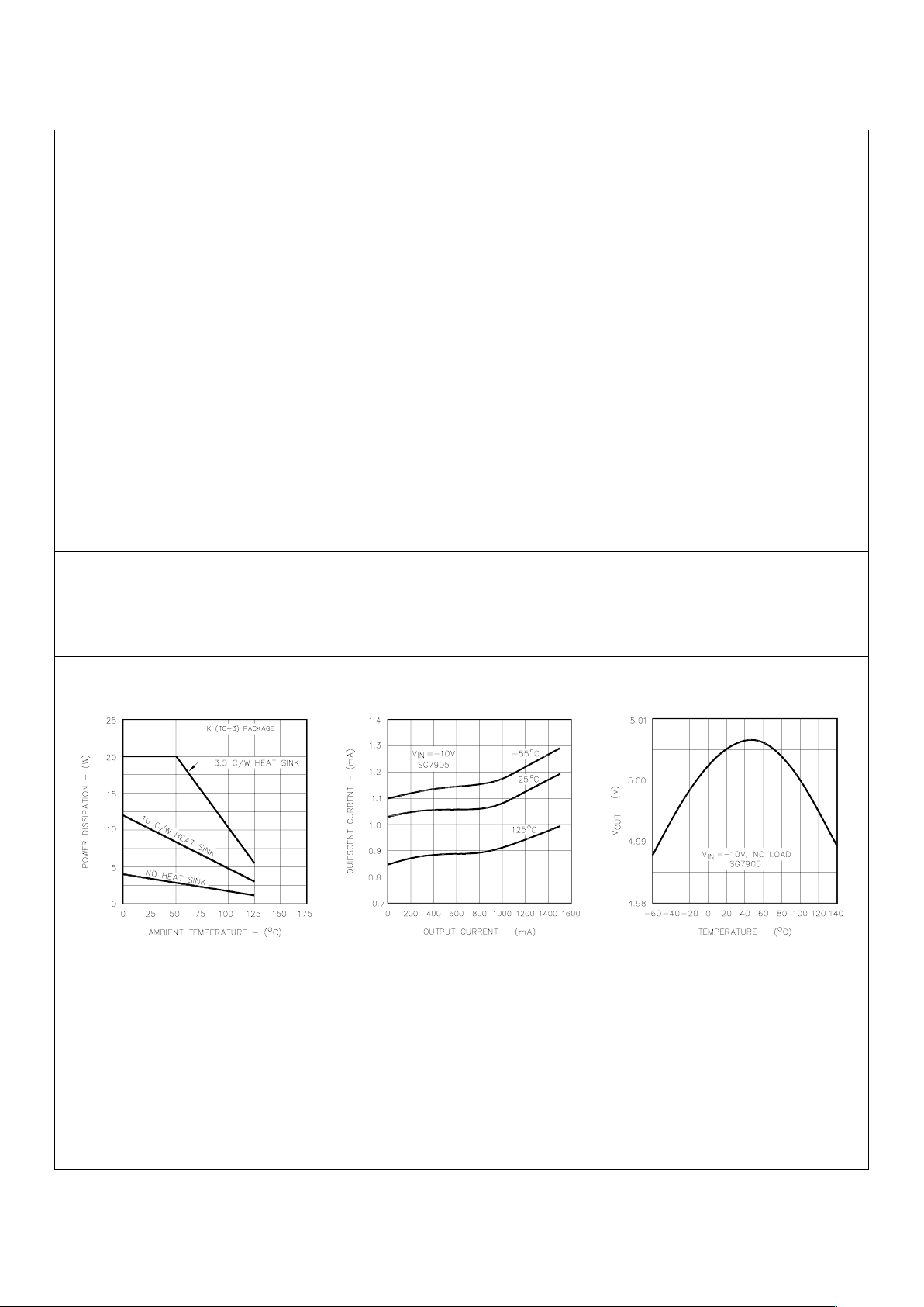
FIGURE 1.
MAXIMUM AVERAGE POWER DISSIPATION
FIGURE 2.
QUIESCENT CURRENT VS. LOAD
FIGURE 3.
TEMPERATURE COEFFICIENT
Note 2. Range over which the device is functional.
CHARACTERISTIC CURVES
-55°C to 150°C
Operating Junction Temperature Range:
SG7900A/7900 .............................................
RECOMMENDED OPERATING CONDITIONS (Note 2)
SG7900A/SG7900 SERIES
12/91 Rev 1.4 12/99 LINFINITY Microelectronics Inc.
Copyright 1999 11861 Western Avenue
∞ ∞
∞ ∞
∞ Garden Grove, CA 92841
3 (714) 898-8121
∞∞
∞∞
∞FAX: (714) 893-2570
FIGURE 6.
SHORT CIRCUIT CURRENT VS. V
IN
CHARACTERISTIC CURVES (continued)
FIGURE 4.
SHORTCIRCUIT CURRENT VS. V
IN
FIGURE 5.
QUIESCENT CURRENT VS. V
IN
FIGURE 7.
DROPOUT CHARACTERISTICS
FIGURE 8.
RIPPLE REJECTION VS. FREQUENCY
APPLICATIONS
FIGURE 9 - FIXED OUTPUT REGULATOR
FIGURE 10 - CIRCUIT FOR INCREASING OUTPUT VOLTAGE
NOTE: 1. C1 is required only if regulator is separated from rectifier filter.
2. Both C1 and C2 should be low E.S.R. types such as solid
tantalum. If aluminum electrolytics are used, at least 10 times
values shown should be selected.
3. If large output capacities are used, the regulators must be
protected from momentary input shorts. A high current diode
NOTE: C3 optional for improved transient response and ripple rejec
R
2
=
V(REG)
15mA
V
OUT
= V (REGULATOR)
R
1
+ R
2
R
1
NEGATIVE REGULATOR
 Loading...