


SG1540Y-883B
Microsemi Corporation SG1540Y-883B, SG2540DW, SG2540M, SG2540Y, SG3540DW Datasheet
...
4/90 Rev 1.1 2/94 LINFINITY Microelectronics Inc.
Copyright 1994 11861 Western Avenue
∞ ∞
∞ ∞
∞ Garden Grove, CA 92841
1 (714) 898-8121
∞∞
∞∞
∞ FAX: (714) 893-2570
SG1540/SG2540/SG3540
OFF-LINE START-UP CONTROLLER
FEATURES
••
••
• Useable with primary and secondary side PWM
controllers
••
••
• Micropower comparator / switch
- Internal 2.5V bandgap reference
- 50mA power switch
••
••
• Squarewave oscillator
- 500Hz to 200KHz operation
- 200mA totem pole outputs
••
••
• Eliminates bulky, expensive 50/60 Hz transformer
••
••
• Minimizes high voltage bleeder current
••
••
• Programmable start-up voltage and hysteresis
••
••
• Internal and programmable overvoltage crowbar
latch
••
••
• Available in 8 pin DIP, 10 pin flat pack, and 16 pin
widebody SOIC
HIGH RELIABILITY FEATURES - SG1540
♦♦
♦♦
♦ Available to MIL-STD - 883
♦♦
♦♦
♦ LMI level "S" processing available
DESCRIPTION
The SG1540 is an integrated circuit designed to efficiently provide
start-up power from a high-voltage DC bus to a PWM control circuit
in a switching power supply. When used on the primary side, it
reduces start-up current to less than 1mA and allows any standard
PWM control circuit to be used as a primary-side controller. When
used to power a controller on the secondary side, it efficiently
eliminates the need for a heavy 50/60Hz line transformer with its
associated low frequency magnetic fields.
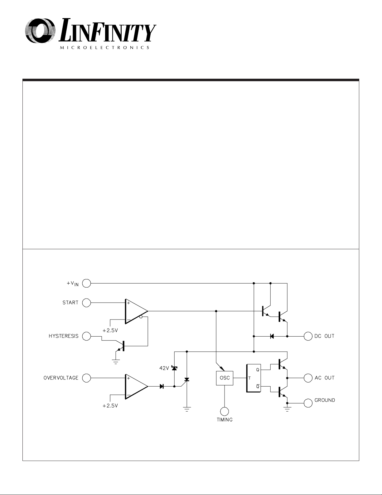
The circuit consists of three sections: a micropower bandgap
comparator/power switch referenced to 2.5 volts which isolates the
start-up capacitor from its load; a high frequency square-wave
oscillator with 200mA totem-pole output for driving an isolation
transformer; and a second bandgap comparator with latching
crowbar to protect against overvoltage faults while starting or
running.
The SG1540 is specified for operation over the full military ambient
temperature range of -55°C to 125°C. The SG2540 is character-
ized for the industrial range of -25°C to 85°C, and the SG3540 is
designed for the commercial range of 0°C to 70°C.
BLOCK DIAGRAM
4/90 Rev 1.1 2/94 LINFINITY Microelectronics Inc.
Copyright 1994 11861 Western Avenue
∞ ∞
∞ ∞
∞ Garden Grove, CA 92841
2 (714) 898-8121
∞∞
∞∞
∞ FAX: (714) 893-2570
SG1540/SG2540/SG3540
Overvoltage Crowbar Energy (½CV²)................................. 8mJ
Operating Junction Temperature
Hermetic (Y Package) ................................................ 150°C
Plastic (M, DW Packages) .......................................... 150°C
Storage Temperature Range ............................ -65°C to 150°C
Lead Temperature (Soldering, 10 Seconds) .................. 300°C
Supply Voltage (+V
IN
)........................................................ +37V
DC Output Current, Continuous (V
OUT
)........................... 100mA
AC Output Current, Continuous ..................................... 200mA
Analog Inputs (Start and Overvoltage) .................-0.3V to 6.0V
Analog Input Currents (V>8V).......................................... 10mA
Overvoltage Crowbar Current, Continuous ..................... 50mA
Note 1. Values beyond which damage may occur.
ABSOLUTE MAXIMUM RATINGS (Note 1)
Y Package:
Thermal Resistance-
Junction to Case, θ
JC
.................. 50°C/W
Thermal Resistance-
Junction to Ambient, θ
JA
............ 130°C/W
M Package:
Thermal Resistance-
Junction to Case, θ
JC
.................. 60°C/W
Thermal Resistance-
Junction to Ambient, θ
JA
............. 95°C/W
DW Package:
Thermal Resistance-
Junction to Case, θ
JC
.................. 40°C/W
Thermal Resistance-
Junction to Ambient, θ
JA
............. 95°C/W
THERMAL DATA
Note A. Junction Temperature Calculation: T
J
= T
A
+ (P
D
x θ
JA
).
Note B. The above numbers for θ
JC
are maximums for the limiting
thermal resistance of the package in a standard mount-
ing configuration. The θ
JA
numbers are meant to be
guidelines for the thermal performance of the device/pc-
board system. All of the above assume no ambient
airflow.
Timing Capacitor Range ........................................ 1nF to 20µF
Operating Ambient Temperature Range
SG1540 ...........................................................-55°C to 125°C
SG2540 .............................................................-25°C to 85°C
SG3540 ................................................................ 0°C to 70°C
Supply Voltage Range ............................................... 7V to 35V
DC Output Current, Continuous................................ 0 to 50mA
AC Output Current, Continuous ............................. 0 to 100 mA
Oscillator Frequency Range ........................... 1KHz to 400KHz
Timing Resistor Range ...................................... 2KΩ to 150KΩ
Note 2. Range over which the device is functional.
RECOMMENDED OPERATING CONDITIONS (Note 2)
ELECTRICAL CHARACTERISTICS
(Unless otherwise specified, these specifications apply over the operating ambient temperatures for SG1540 with -55°C ≤ T
A
≤ 125°C, SG2540 with
-25°C ≤ T
A
≤ 85°C, SG3540 with 0°C ≤ T
A
≤ 70°C, and +V
IN
= 15V. A 0.1µF high frequency bypass capacitor is recommended on V
IN
. Low duty cycle
testing techniques are used which maintains junction and case temperatures equal to the ambient temperature.)
Units
Typ. Max.
V
START
= 0 to 2.37V
V
TIMING
= +V
IN
; V
OUT
Open
F
OSC
= 50KHz, V
OUT
and AC
OUT
Open
V
PIN 1
= 0 to 5V
I
PIN 1
= 1mA
I
PIN 4
= 100µA
2.37
6
0.2
0.3
3
2.50
0.1
7
0.1
0.4
0.6
6
2.63
1
8
0.2
mA
mA
mA
V
µA
V
V
Start-up Section
Start Current I
CC
Operating Current
Start Threshold
Start Bias Current
Start Clamp Voltage
Hysteresis ON Voltage
DC Output Section
Min.
SG1540/2540/3540
Test ConditionsParameter
V
OUT
Voltage
Short Circuit Current
12.5
12.0
50
13.5
13.0
100 225
V
V
mA
I
SOURCE
= 10mA
I
SOURCE
= 50mA
V
OUT
= 0V
 Loading...