


Microsemi Corporation SG1844Y, SG1844Y-883B, SG1844Y-DESC, SG1845F-DESC, SG1845J Datasheet
...
|
|
LIN D O C #: 1844 |
|
|
|
|
|
|
|
|
|
SG1844/SG1845 Series |
|
|
|
|
|
|
|
|
|
C U R R E N T M O D E P W M C O N T R O L L E R |
|
|
|
|
|
|
|
T H E I N F I N I T E P O W E R O F I N N O V A T I O N |
P R O D U C T I O N D A T A S H E E T |
|
|
|
D E S C R I P T I O N
The SG1844/45 family of control ICs provides all the necessary features to implement off-line fixed frequency, current-mode switching power supplies with a minimum number of external components. Current-mode architecture demonstrates improved line regulation, improved load regulation, pulse-by- pulse current limiting and inherent protection of the power supply output switch.
The bandgap reference is trimmed to ±1% over temperature. Oscillator discharge current is trimmed to less than ±10%. The SG1844/45 has undervoltage lockout, current-limiting circuitry
and start-up current of less than 1mA. The totem-pole output is optimized to
drive the gate of a power MOSFET. The output is low in the off state to provide direct interface to an N-channel device.
Both operate up to a maximum duty cycle range of zero to <50% due to an internal toggle flip-flop which blanks the output off every other clock cycle.
The SG1844/45 is specified for operation over the full military ambient temperature range of -55°C to 125°C. The SG2844/45 is specified for the industrial range of -25°C to 85°C, and the SG3844/45 is designed for the commercial range of 0°C to 70°C.
|
P R O D U C T H I G H L I G H T |
TY P I C A L AP P L I C AT I O N O F SG3844 IN A FLY B A C K CO N V E R T E R |
|
|
RST |
AC |
IST |
INPUT |
VCC |
|
|
K E Y F E AT U R E S
■OPTIMIZED FOR OFF-LINE CONTROL
■LOW START-UP CURRENT (<1mA)
■AUTOMATIC FEED FORWARD
COMPENSATION
■TRIMMED OSCILLATOR DISCHARGE
CURRENT
■PULSE-BY-PULSE CURRENT LIMITING
■ENHANCED LOAD RESPONSE
CHARACTERISTICS
■UNDER-VOLTAGE LOCKOUT WITH 6V HYSTERESIS (SG1844 only)
■DOUBLE PULSE SUPPRESSION
■HIGH-CURRENT TOTEM-POLE OUTPUT
■INTERNALLY TRIMMED BANDGAP REFERENCE
■500kHz OPERATION
■UNDERVOLTAGE LOCKOUT
SG1844 - 16 volts SG1845 - 8.4 volts
■LOW SHOOT-THROUGH CURRENT <75mA
OVER TEMPERATURE
HIGH RELIABILITY FEATURES
■AVAILABLE TO MIL-STD-883B
■LINFINITY LEVEL "S" PROCESSING AVAILABLE
SG3844
PA C K A G E O R D E R I N F O R M AT I O N
TA (°C) |
M |
Plastic DIP |
|
N |
|
Plastic DIP |
|
DM |
Plastic SOIC |
|
D |
Plastic SOIC |
|
Y |
Ceramic DIP |
J |
Ceramic DIP |
|
F |
Cer. Flatpack |
|
L |
Ceramic LCC |
||||
8-pin |
|
|
14-pin |
|
8-pin |
|
14-pin |
|
8-pin |
14-pin |
|
10-pin |
|
20-pin |
|||||||||||||
|
|
|
|
|
|
|
|
|
|
|
|
|
|
|
|
|
|
|
|
|
|
|
|
|
|
|
|
0 to 70 |
SG3844M |
|
|
SG3844N |
|
|
SG3844DM |
|
|
SG3844D |
|
SG3844Y |
|
SG3844J |
|
|
— |
|
|
— |
|||||||
|
|
|
|
|
|
|
|
|
|
|
|
|
|
|
|
|
|
|
|
|
|
|
|
|
|
||
SG3845M |
|
|
SG3845N |
|
|
SG3845DM |
|
|
SG3845D |
|
SG3845Y |
|
SG3845J |
|
|
— |
|
|
— |
||||||||
|
|
|
|
|
|
|
|
|
|
|
|
|
|
||||||||||||||
|
|
|
|
|
|
|
|
|
|
|
|
|
|
|
|
|
|
|
|
|
|
|
|
|
|
|
|
-25 to 85 |
SG2844M |
|
|
SG2844N |
|
|
SG2844DM |
|
|
SG2844D |
|
SG2844Y |
|
SG2844J |
|
|
— |
|
|
— |
|||||||
|
|
|
|
|
|
|
|
|
|
|
|
|
|
|
|
|
|
|
|
|
|
|
|
|
|
||
SG2845M |
|
|
SG2845N |
|
|
SG2845DM |
|
|
SG2845D |
|
SG2845Y |
|
SG2845J |
|
|
— |
|
|
— |
||||||||
|
|
|
|
|
|
|
|
|
|
|
|
|
|
||||||||||||||
-55 to 125 |
|
— |
|
|
|
— |
|
|
|
— |
|
|
— |
|
SG1844Y |
|
SG1844J |
|
|
— |
|
SG1844L |
|
||||
|
— |
|
|
|
— |
|
|
|
— |
|
|
— |
|
SG1845Y |
|
SG1845J |
|
|
— |
|
SG1845L |
|
|||||
|
|
|
|
|
|
|
|
|
|
|
|
|
|
|
|
||||||||||||
MIL-STD/883 |
|
— |
|
|
|
— |
|
|
|
— |
|
|
— |
|
SG1844Y/883B |
SG1844J/883B |
|
|
— |
|
SG1844L/883B |
|
|||||
|
— |
|
|
|
— |
|
|
|
— |
|
|
— |
|
SG1845Y/883B |
SG1845J/883B |
|
|
— |
|
SG1845L/883B |
|
||||||
|
|
|
|
|
|
|
|
|
|
|
|
|
|
|
|||||||||||||
DESC |
|
— |
|
|
|
— |
|
|
|
— |
|
|
— |
|
SG1844Y/DESC |
SG1844J/DESC |
|
SG1844F/DESC |
|
SG1844L/DESC |
|
||||||
|
|
|
|
|
|
|
|
|
— |
|
|
— |
|
SG1845Y/DESC |
SG1845J/DESC |
|
SG1845F/DESC |
|
SG1845L/DESC |
|
|||||||
|
|
|
|
|
|
|
|
|
|
|
|
|
|
|
|
||||||||||||
|
|
|
|
|
|
|
|
|
|
|
|
|
|
|
|
|
|
|
|
|
|
|
|
|
|
|
|
Note: All surface-mount packages are available in Tape & Reel.
F O R F U R T H E R I N F O R M AT I O N C A L L ( 7 1 4 ) 8 9 8 - 8 1 2 1
Copyright © 2000 |
11861 WESTERN AVENUE, GARDEN GROVE, CA. 92841 |
1 |
Rev. 1.4 4/00 |
|
|

P R O D U C T D A T A B O O K 1 9 9 6 / 1 9 9 7
SG1844/SG1845 Series
C U R R E N T - M O D E P W M C O N T R O L L E R
P R O D U C T I O N D A T A S H E E T
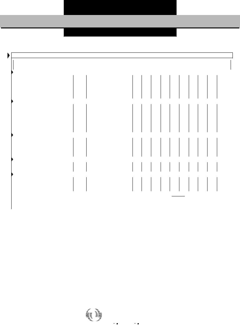
ABSOLUTE MAXIMUM RATINGS |
(Notes 1 & 2) |
|
Supply Voltage (ICC < 30mA) ............................................................... |
Self Limiting |
|
Supply Voltage (Low Impedance Source) ........................................................ |
30V |
|
Output Current (Peak) ....................................................................................... |
±1A |
|
Output Current (Continuous) ....................................................................... |
350mA |
|
Output Energy (Capacitive Load) ....................................................................... |
5µJ |
|
Analog Inputs (Pins 2, 3) ................................................................. |
-0.3V to +6.3V |
|
Error Amp Output Sink Current ..................................................................... |
10mA |
|
Operating Junction Temperature |
|
|
Hermetic (J, Y, F, L Packages) ................................................................... |
150°C |
|
Plastic (N, M, D, DM Packages) ................................................................ |
150°C |
|
Storage Temperature Range .......................................................... |
-65°C to +150°C |
|
Lead Temperature (Soldering, 10 Seconds) .................................................. |
300°C |
Note 1. Exceeding these ratings could cause damage to the device.
Note 2. All voltages are with respect to Pin 5. All currents are positive into the specified terminal.
THERMAL DATA
M PACKAGE:
THERMAL RESISTANCE-JUNCTION TO AMBIENT, θJA |
95°C/W |
N PACKAGE: |
|
THERMAL RESISTANCE-JUNCTION TO AMBIENT, θJA |
65°C/W |
DM PACKAGE: |
|
THERMAL RESISTANCE-JUNCTION TO AMBIENT, θJA |
165°C/W |
D PACKAGE: |
|
THERMAL RESISTANCE-JUNCTION TO AMBIENT, θJA |
120°C/W |
Y PACKAGE: |
|
THERMAL RESISTANCE-JUNCTION TO AMBIENT, θJA |
130°C/W |
J PACKAGE: |
|
THERMAL RESISTANCE-JUNCTION TO AMBIENT, θJA |
80°C/W |
F PACKAGE: |
|
THERMAL RESISTANCE-JUNCTION TO CASE, θJC |
80°C/W |
THERMAL RESISTANCE-JUNCTION TO AMBIENT, θJA |
145°C/W |
L PACKAGE: |
|
THERMAL RESISTANCE-JUNCTION TO CASE, θJC |
35°C/W |
THERMAL RESISTANCE-JUNCTION TO AMBIENT, θJA |
120°C/W |
Junction Temperature Calculation: TJ = TA + (PD x θJA).
The θJA numbers are guidelines for the thermal performance of the device/pc-board system. All of the above assume no ambient airflow.
PACKAGE PIN OUTS
COM |
|
1 |
8 |
|
VREF |
|
|
||||
VFB |
|
2 |
7 |
|
VCC |
|
|
||||
ISENSE |
|
3 |
6 |
|
OUT UT |
|
|
||||
RT/CT |
|
4 |
5 |
|
GND |
|
|
M & Y PACKAGE
(Top View)
COM |
|
|
|
1 |
8 |
|
|
VREF |
|
|
|
|
|||||
VFB |
|
|
|
2 |
7 |
|
|
VCC |
|
|
|
|
|||||
ISENSE |
|
|
|
3 |
6 |
|
|
OUT UT |
|
|
|
|
|
|
|
||
RT/CT |
|
|
|
4 |
5 |
|
|
GND |
|
|
|
|
|
|
|
DM PACKAGE
(Top View)
COM |
|
|
|
1 |
14 |
|
|
VREF |
|
|
|
|
|
||||
N.C. |
|
|
|
2 |
13 |
|
|
N.C. |
|
|
|
|
|||||
VFB |
|
|
|
3 |
12 |
|
|
VCC |
|
|
|
|
|||||
|
|
|
|
|||||
N.C. |
|
|
|
4 |
11 |
|
|
VC |
|
|
|
|
|||||
ISENSE |
|
|
|
5 |
10 |
|
|
OUT UT |
|
|
|
|
|||||
N.C. |
|
|
|
6 |
9 |
|
|
GND |
RT/CT |
|
|
|
7 |
8 |
|
|
WR GND |
|
|
|
|
|||||
|
|
|
|
D PACKAGE
(Top View)
|
|
|
COM |
|
1 |
|
14 |
|
VREF |
|
|
|
|||||
|
|
|
|
N.C. |
2 |
|
13 |
|
N.C. |
|
|
|
|||||
|
|
|
|
VFB |
3 |
|
12 |
|
VCC |
|
|
|
|||||
|
|
|
|
N.C. |
4 |
|
11 |
|
VC |
|
|
|
|||||
|
|
|
|
ISENSE |
5 |
|
10 |
|
OUT UT |
|
|
|
|||||
|
|
|
|
N.C. |
6 |
|
9 |
|
GROUND |
|
|
|
|||||
|
|
|
|
RT/CT |
7 |
|
8 |
|
OWER GND |
|
|
||||||
|
|
|
|
J & N PACKAGE |
|
|
|
||||||||||
|
|
|
|
|
|
(Top View) |
|
|
|
|
|
|
|||||
1. COM |
|
|
|
|
|
|
|
|
|
|
|
|
|
|
10.VREF |
||
2. VFB |
|
|
|
|
|
|
1 |
|
10 |
|
|
|
|
||||
|
|
|
|
|
|
2 |
|
9 |
|
|
|
|
9. |
VCC |
|||
|
|
|
|
|
|
|
|
|
|
|
|||||||
|
|
|
|
|
|
|
|
|
|
|
|||||||
3. ISENSE |
|
|
|
|
|
|
3 |
|
8 |
|
|
|
|
8. |
VC |
||
|
|
|
|
|
|
|
|
|
|
|
|||||||
|
|
|
|
|
|
|
|
|
|
|
|||||||
4. RT/CT |
|
|
|
|
|
|
4 |
|
7 |
|
|
|
|
7. |
OUT UT |
||
|
|
|
|
|
|
|
|
|
|
|
|||||||
|
|
|
|
|
|
5 |
|
6 |
|
|
|
|
|||||
5. OWER GND |
|
|
|
|
|
|
|
|
|
|
6. GND |
||||||
|
|
|
|
|
|
|
|
|
|
||||||||
|
|
|
F PACKAGE |
|
|
|
|||||||||||
|
|
|
|
|
|
|
|
|
|
|
|||||||
|
|
|
|
|
|
(Top View) |
|
|
|
|
|
|
|||||
3 |
2 |
1 |
20 |
19 |
|
|
|
1. |
N.C. |
|
11. |
N.C. |
|||||
|
|
|
|
|
|
|
|
|
|
2. |
N.C. |
|
12. |
WR GND |
|||
4 |
|
|
|
|
|
|
|
18 |
|
3. |
COM . |
|
13. |
GND |
|||
5 |
|
|
|
|
|
|
|
17 |
|
4. |
N.C. |
|
14. |
N.C. |
|||
|
|
|
|
|
|
|
|
5. |
VFB |
|
15. |
OUT UT |
|||||
6 |
|
|
|
|
|
|
|
16 |
|
|
|||||||
|
|
|
|
|
|
|
|
6. |
N.C. |
|
16. |
N.C. |
|||||
|
|
|
|
|
|
|
|
|
|
|
|||||||
7 |
|
|
|
|
|
|
|
15 |
|
7. |
ISENSE |
|
17. |
VC |
|||
8 |
|
|
|
|
|
|
|
14 |
|
|
|||||||
|
|
|
|
|
|
|
|
8. |
RT/CT |
|
18. |
VCC |
|||||
|
|
|
|
|
|
|
|
|
|
9. |
N.C. |
|
19. |
N.C. |
|||
9 |
10 |
11 |
12 |
13 |
|
|
|
|
10. N.C. |
|
20. |
VREF |
|||||
|
|
|
|
|
|
|
|
|
|
||||||||
L PACKAGE
(Top View)
2 |
|
Copyright © 2000 |
|
Rev. 1.4 4/00 |
|
|
|
|

P R O D U C T D A T A B O O K 1 9 9 6 / 1 9 9 7
SG1844/SG1845 Series
C U R R E N T - M O D E P W M C O N T R O L L E R
P R O D U C T I O N D A T A S H E E T
|
|
R E C O M M E N D E D |
O P E R AT I N G |
C O N D I T I O N S |
(Note 3) |
|
|
|
|||
|
|
|
|
|
|
|
|
|
|
|
|
|
|
Parameter |
|
Symbol |
|
Recommended Operating Conditions |
Units |
|
|||
|
|
|
|
Min. |
Typ. |
Max. |
|
||||
|
|
|
|
|
|
|
|
||||
|
|
|
|
|
|
|
|
|
|
|
|
|
Supply Voltage Range |
|
|
|
|
|
30 |
|
V |
|
|
|
Output Current (Peak) |
|
|
|
|
|
±1 |
|
A |
|
|
|
Output Current (Continuous) |
|
|
|
|
|
200 |
|
mA |
|
|
|
Analog Inputs (Pin 2, Pin 3) |
|
|
|
0 |
|
|
2.6 |
V |
|
|
|
Error Amp Output Sink Current |
|
|
|
|
|
5 |
|
mA |
|
|
|
Oscillator Frequency Range |
|
|
|
0.1 |
|
|
500 |
kHz |
|
|
|
Oscillator Timing Resistor |
|
RT |
|
0.52 |
|
|
150 |
kΩ |
|
|
|
Oscillator Timing Capacitor |
|
CT |
|
0.1 |
|
|
1.0 |
µF |
||
|
Operating Ambient Temperature Range: |
|
|
|
|
|
|
|
|
|
|
|
|
SG1844/45 |
|
|
|
-55 |
|
|
125 |
°C |
|
|
|
SG2844/45 |
|
|
|
-25 |
|
|
85 |
°C |
|
|
|
SG3844/45 |
|
|
|
0 |
|
|
70 |
°C |
|
Note 3. Range over which the device is functional.
E L E C T R I C A L C H A R A C T E R I S T I C S
(Unless otherwise specified, these specifications apply over the operating ambient temperatures for SG1844/SG1845 with -55°C ≤ TA ≤ 125°C, SG2844/ SG2845 with -25°C ≤ TA ≤ 85°C, SG3844/SG3845 with 0°C ≤ TA ≤ 70°C, VCC = 15V (Note 7), RT = 10kΩ, and CT = 3.3nF. Low duty cycle pulse testing techniques are used which maintains junction and case temperatures equal to the ambient temperature.)
Parameter |
Symbol |
Test Conditions |
SG1844/45 |
SG2844/45 |
SG3844/45 |
Units |
|||||||
Min. Typ. Max. Min. Typ. Max. Min. Typ. Max. |
|||||||||||||
Reference Section |
|
|
|
|
|
|
|
|
|
|
|
|
|
|
|
|
|
|
|
|
|
|
|
|
|
|
|
Output Voltage |
|
|
TJ = 25°C, IO = 1mA |
4.95 |
5.00 |
5.05 |
4.95 |
5.00 |
5.05 |
4.90 |
5.00 |
5.10 |
V |
Line Regulation |
|
|
12 ≤ VIN ≤ 25V |
|
6 |
20 |
|
6 |
20 |
|
6 |
20 |
mV |
Load Regulation |
|
|
1 ≤ IO ≤ 20mA |
|
6 |
25 |
|
6 |
25 |
|
6 |
25 |
mV |
Temperature Stability |
(Note 4) |
|
|
|
0.2 |
0.4 |
|
0.2 |
0.4 |
|
0.2 |
0.4 |
mV/°C |
Total Output Variation (Note 4) |
|
Line, Load, Temp. |
4.90 |
|
5.10 |
4.90 |
|
5.10 |
4.82 |
|
5.18 |
V |
|
Output Noise Voltage |
(Note 4) |
VN |
10Hz ≤ f ≤ 10kHz, TJ = 25°C |
|
50 |
|
|
50 |
|
|
50 |
|
µV |
Long Term Stability (Note 4) |
|
TA = 125°C, 1000hrs |
|
5 |
25 |
|
5 |
25 |
|
5 |
25 |
mV |
|
Output Short Circuit |
|
|
|
-30 |
-100 |
-180 |
-30 |
-100 |
-180 |
-30 |
-100 |
-180 |
mA |
Oscillator Section |
|
|
|
|
|
|
|
|
|
|
|
|
|
|
|
|
|
|
|
|
|
|
|
|
|
|
|
Initial Accuracy (Note 8) |
|
TJ = 25°C |
47 |
52 |
57 |
47 |
52 |
57 |
47 |
52 |
57 |
kHz |
|
Voltage Stability |
|
|
12V ≤ VCC ≤ 25V |
|
.02 |
1 |
|
0.2 |
1 |
|
0.2 |
1 |
% |
Temperature Stability |
(Note 4) |
|
TMIN ≤ TA ≤ TMAX |
|
5 |
|
|
5 |
|
|
5 |
|
% |
Amplitude |
|
|
VRT/CT (Peak to Peak) |
|
1.7 |
|
|
1.7 |
|
|
1.7 |
|
V |
Discharge Current |
|
|
TJ = 25°C |
7.8 |
8.3 |
9.1 |
7.5 |
8.4 |
9.3 |
7.5 |
8.4 |
9.3 |
mA |
|
|
|
TMIN ≤ TA ≤ TMAX |
6.8 |
|
9.3 |
7.2 |
|
9.5 |
7.2 |
|
9.5 |
mA |
Error Amp Section |
|
|
|
|
|
|
|
|
|
|
|
|
|
|
|
|
|
|
|
|
|
|
|
|
|
|
|
Input Voltage |
|
|
VCOMP = 2.5V |
2.45 |
2.50 |
2.55 |
2.45 |
2.50 |
2.55 |
2.42 |
2.50 |
2.58 |
V |
Input Bias Current |
|
|
|
|
-0.3 |
-1 |
|
-0.3 |
1 |
|
-0.3 |
-2 |
µA |
Open Loop Gain |
|
AVOL |
2 ≤ VO ≤ 4V |
65 |
90 |
|
65 |
90 |
|
65 |
90 |
|
dB |
Unity Gain Bandwidth |
(Note 4) |
|
TJ = 25°C |
0.7 |
1 |
|
0.7 |
1 |
|
0.7 |
1 |
|
MHz |
Power Supply Rejection Ratio |
PSRR |
12 ≤ VCC ≤ 25V |
60 |
70 |
|
60 |
70 |
|
60 |
70 |
|
dB |
|
Output Sink Current |
|
|
VVFB = 2.7V, VCOMP = 1.1V |
2 |
6 |
|
2 |
6 |
|
2 |
6 |
|
mA |
Output Source Current |
|
VVFB = 2.3V, VCOMP = 5V |
-0.5 |
-0.8 |
|
-0.5 |
-0.8 |
|
-0.5 |
-0.8 |
|
mA |
|
VOUT High |
|
|
VVFB = 2.3V, RL = 15K to gnd |
5 |
6 |
|
5 |
6 |
|
5 |
6 |
|
V |
VOUT Low |
|
|
VVFB = 2.7V, RL = 15K to VREF |
|
0.7 |
1.1 |
|
0.7 |
1.1 |
|
0.7 |
1.1 |
V |
( E l e c t r i c a l C h a r a c t e r i s t i c s c o n t i n u e n e x t p a g e . )
Copyright © 2000 |
3 |
Rev. 1.4 4/00 |
P R O D U C T D A T A B O O K 1 9 9 6 / 1 9 9 7
SG1844/SG1845 Series
C U R R E N T - M O D E P W M C O N T R O L L E R
P R O D U C T I O N D A T A S H E E T
|
|
|
|
|
|
|
|
|
|
|
|
|
|
|
|
|
|
|
|
|
|
|
|
|
|
|
|
|
|
|
|
|
Parameter |
Symbol |
Test Conditions |
SG1844/45 |
SG2844/45 |
SG3844/45 |
Units |
|
|||||||
|
|
||||||||||||||
|
Min. Typ. Max. Min. Typ. Max. Min. Typ. Max. |
|
|||||||||||||
|
Current Sense Section |
|
|
|
|
|
|
|
|
|
|
|
|
|
|
|
|
|
|
|
|
|
|
|
|
|
|
|
|
|
|
|
Gain (Notes 5 & 6) |
|
|
2.85 |
3 |
3.15 |
2.85 |
3 |
3.15 |
2.85 |
3 |
3.15 |
V/V |
|
|
|
Maximum Input Signal (Note 5) |
|
VCOMP = 5V |
0.9 |
1 |
1.1 |
0.9 |
1 |
1.1 |
0.9 |
1 |
1.1 |
V |
|
|
|
Power Supply Rejection Ratio (Note 5) |
PSRR |
12 ≤ VCC ≤ 25V |
|
70 |
|
|
70 |
|
|
|
70 |
|
dB |
|
|
Input Bias Current |
|
|
|
-2 |
-10 |
|
-2 |
-10 |
|
-2 |
-10 |
µA |
|
|
|
Delay to Output (Note 4) |
|
|
|
150 |
300 |
|
150 |
300 |
|
150 |
300 |
ns |
||
|
Output Section |
|
|
|
|
|
|
|
|
|
|
|
|
|
|
|
|
|
|
|
|
|
|
|
|
|
|
|
|
|
|
|
Output Low Level |
|
ISINK = 20mA |
|
0.1 |
0.4 |
|
0.1 |
0.4 |
|
0.1 |
0.4 |
V |
|
|
|
|
|
ISINK = 200mA |
|
1.5 |
2.2 |
|
1.5 |
2.2 |
|
1.5 |
2.2 |
V |
|
|
|
Output High Level |
|
ISOURCE = 20mA |
13 |
13.5 |
|
13 |
13.5 |
|
|
13 |
13.5 |
|
V |
|
|
|
|
ISOURCE = 200mA |
12 |
13.5 |
|
12 |
13.5 |
|
|
12 |
13.5 |
|
V |
|
|
Rise Time (Note 4) |
|
T J = 25°C, CL = 1nF |
|
50 |
150 |
|
50 |
150 |
|
50 |
150 |
ns |
|
|
|
Fall Time (Note 4) |
|
TJ = 25°C, CL = 1nF |
|
50 |
150 |
|
50 |
150 |
|
50 |
150 |
ns |
||
|
Under-Voltage Lockout Section |
|
|
|
|
|
|
|
|
|
|
|
|
|
|
|
|
|
|
|
|
|
|
|
|
|
|
|
|
|
|
|
Start Threshold |
|
1844 |
15 |
16 |
17 |
15 |
16 |
17 |
14.5 |
16 |
17.5 |
V |
|
|
|
|
|
1845 |
7.8 |
8.4 |
9.0 |
7.8 |
8.4 |
9.0 |
7.8 |
8.4 |
9.0 |
V |
|
|
|
Min. Operation Voltage After Turn-On |
|
1844 |
9 |
10 |
11 |
9 |
10 |
11 |
8.5 |
10 |
11.5 |
V |
|
|
|
|
|
1845 |
7.0 |
7.6 |
8.3 |
7.0 |
7.6 |
8.2 |
7.0 |
7.6 |
8.2 |
V |
||
|
PWM Section |
|
|
|
|
|
|
|
|
|
|
|
|
|
|
|
|
|
|
|
|
|
|
|
|
|
|
|
|
|
|
|
Maximum Duty Cycle |
|
|
46 |
48 |
50 |
46 |
48 |
50 |
46 |
48 |
50 |
% |
|
|
|
Minimum Duty Cycle |
|
|
|
|
0 |
|
|
0 |
|
|
0 |
% |
|
|
|
Power Consumption Section |
|
|
|
|
|
|
|
|
|
|
|
|
|
|
|
|
|
|
|
|
|
|
|
|
|
|
|
|
|
|
|
Start-Up Current |
|
|
|
0.5 |
1 |
|
0.5 |
1 |
|
0.5 |
1 |
mA |
|
|
|
Operating Supply Current |
|
VFB = VISENSE = 0V |
|
11 |
17 |
|
11 |
17 |
|
11 |
17 |
mA |
|
|
|
VCC Zener Voltage |
|
ICC = 25mA |
|
34 |
|
|
34 |
|
|
|
34 |
|
V |
|
|
|
|
|
|
|
|
|
∆ VCOMP |
0 ≤ VISENSE ≤ 0.8V. |
|
|
||||
|
Notes: 4. These parameters, although guaranteed, are not 100% tested in |
6. Gain defined as: A = |
∆ VISENSE |
; |
|
|
|||||||||
|
production. |
|
|
|
|
|
|
|
|
|
|
|
|
|
|
|
E L E C T R I C A L C H A R A C T E R I S T I C S (Cont'd.) |
|
|
|
|
|
|
|
|||||||
5. Parameter measured at trip point of latch with VVFB |
= 0. |
7. |
Adjust VCC above the start threshold before setting at 15V. |
|
8. |
Output frequency equals one half of oscillator frequency. |
|||
|
|
4 |
|
Copyright © 2000 |
|
Rev. 1.4 4/00 |
|
|
|
|
 Loading...