

Page 1

Pod XT Live
Bass Pod XT Live
Service Manual
Page 2

3850-A Royal Ave.
Simi Valley, CA 93063-3380
818-575-3922
818-575-3961 (Fax)
Attention:
Before replacing the mainboard on any
POD XT family unit
(POD XT / POD XT Pro / POD XT Live / Bass POD XT
/ Bass POD XT Pro / Bass POD XT Live)
See Tech Bulletin
#26!!!
Page 3

Technical Bulletin 026:
Product: Pod XT FAMILY;
Pod XT/ Pod XT Pro /Pod XT Live / Bass
Pod XT/ Bass Pod XT Pro/ Bass Pod XT
Live
Application: To be implemented during all main pcba replacements of all Pod XT family
units.
Objective: To ensure each unit’s specific Identification is retained for online use.
Parts affected : Secure Memory IC = 15-79-0088. For Pod XT/ Bass Pod XT = U17. For
Pod XT Pro/ Bass Pod XT Pro = U8. For Pod XT Live/ Bass Pod XT Live = U24.
Tools/Supplies Required: A solder iron with a small tip. Solder.
Procedure : During main board replacement, carefully remove the secure memeory IC
from the old main board (see above for reference designator). Install the secure memory IC
just removed, onto the new main board before installing the new board into the unit.
Warranty Implications : This is a required step of a main board replacement for the Pod
XT Family of units, and can be part of either a warranty or a non – warranty repair.
1
Customer Service Tel: (818) 575-3600 • Customer Service Fax: (818) 676-1585
Line 6 Inc. • 29901 Agoura Road, Agoura Hills, CA 91301 • 6033 De Soto Ave.
Woodland Hills, CA, 91367
Page 4
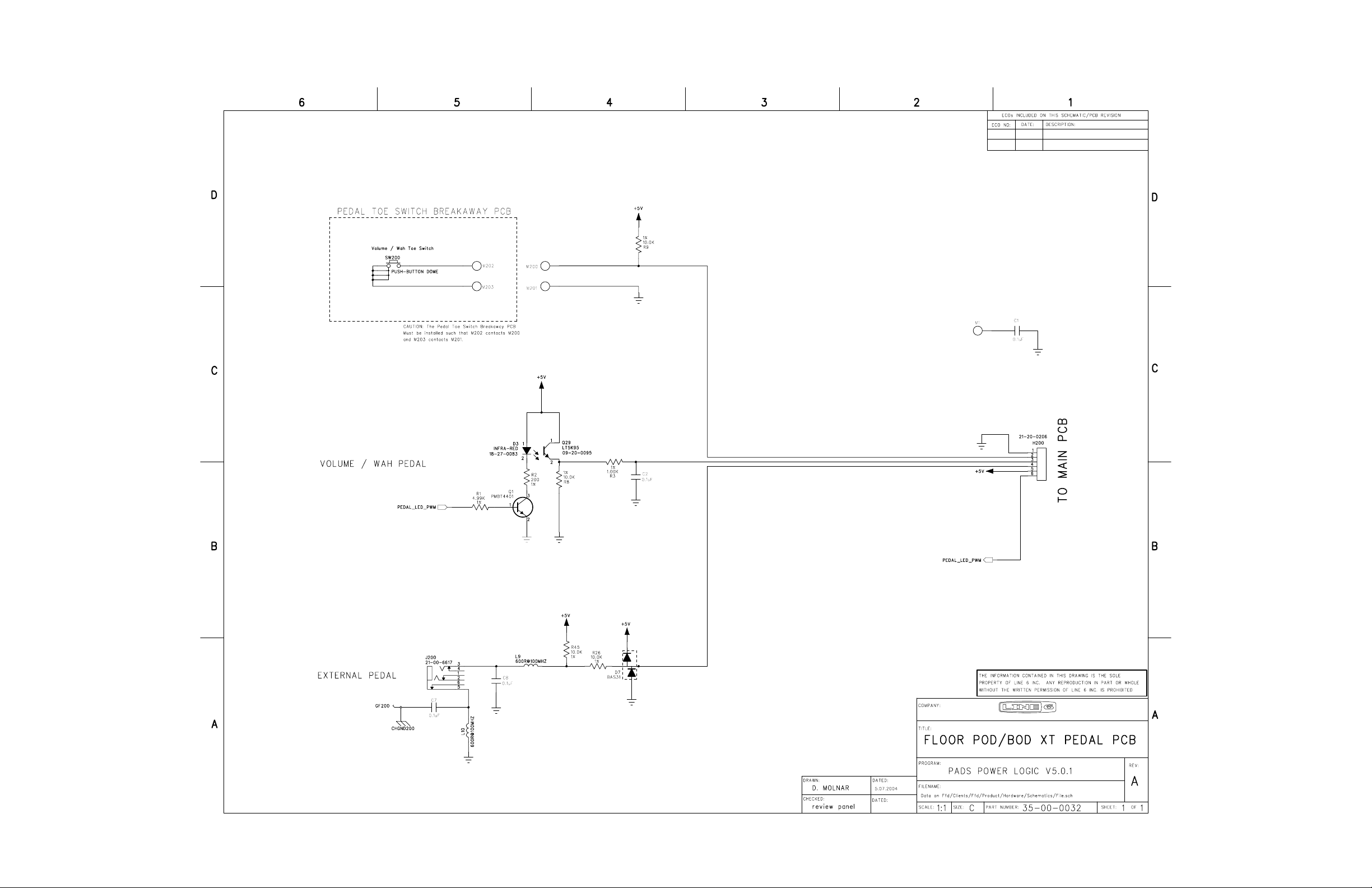
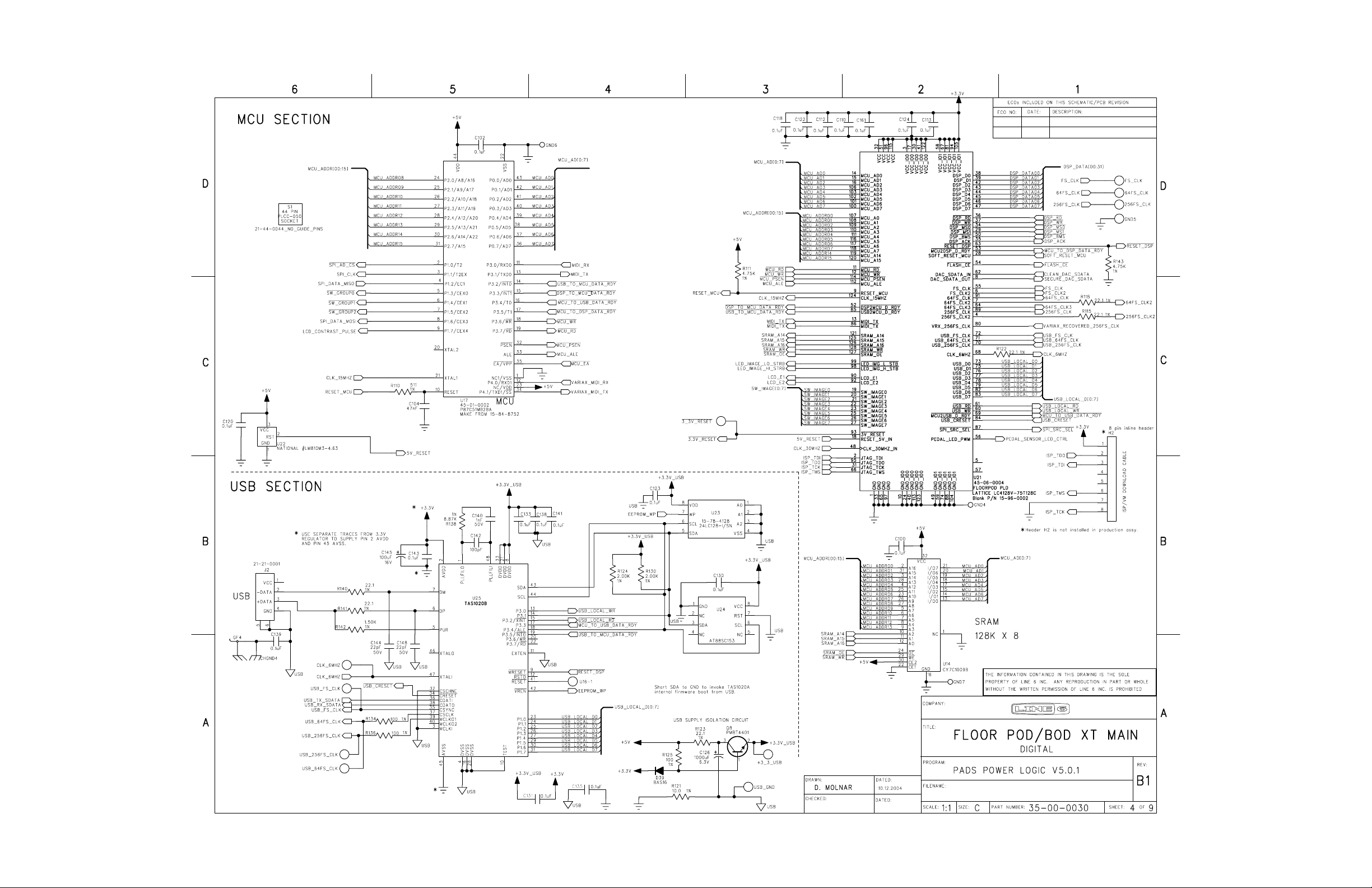
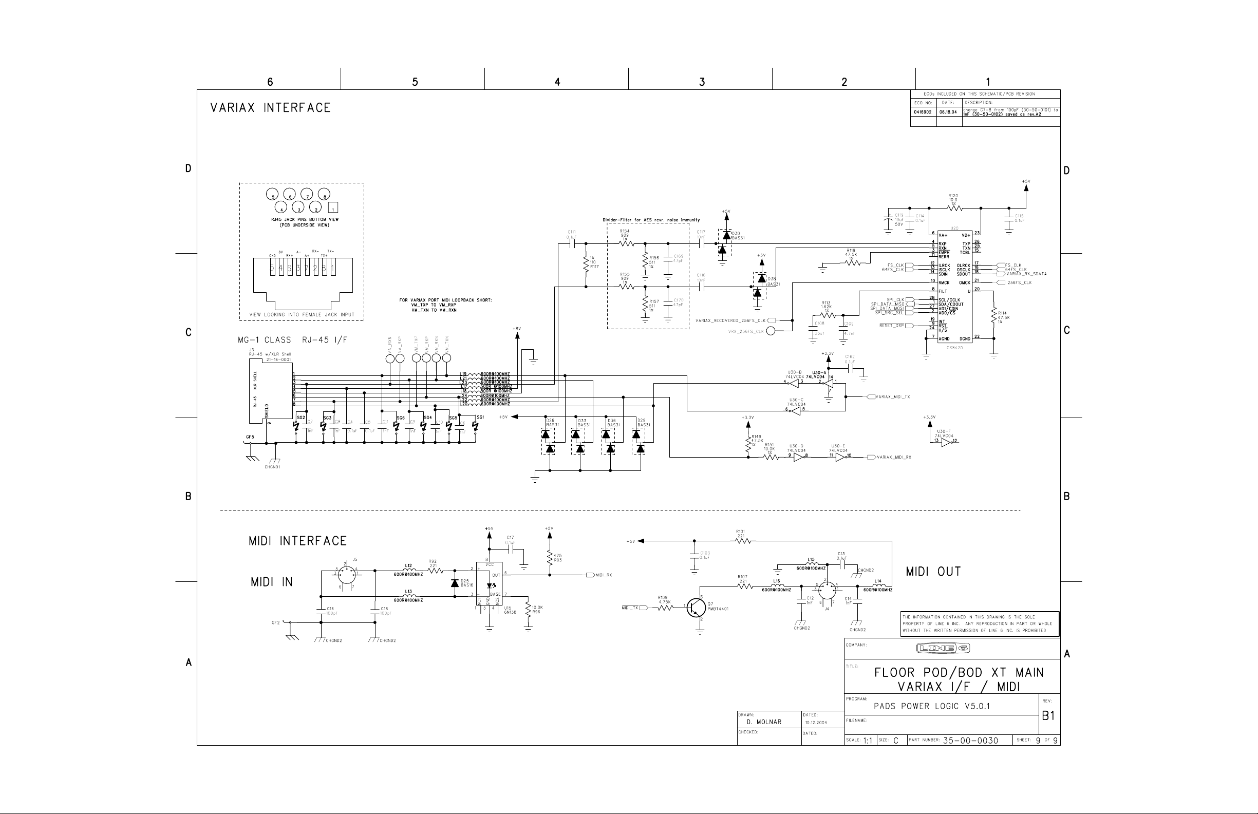
SCHEMATIC FLOORPOD XT PEDAL REV A.sch-1 - Fri May 07 10:58:51 2004
Page 5
Page 6
Page 7
Page 8
Page 9
Page 10
Page 11

Page 12
Page 13
Page 14
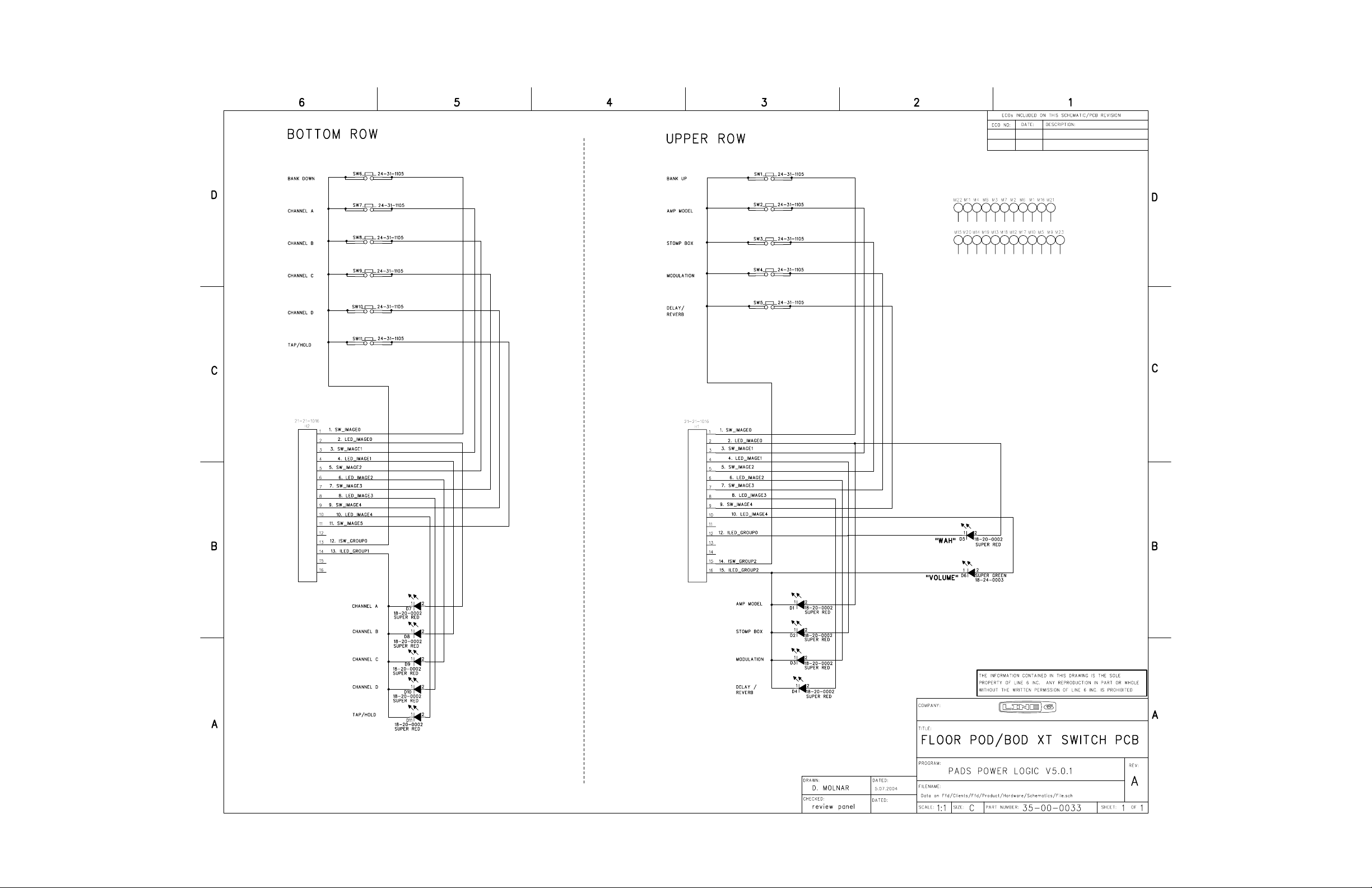
SCHEMATIC FLOORPOD XT SWITCH REV A.sch-1 - Fri May 07 11:00:01 2004
Page 15
99-060-0605 POD XT LIVE Complete Unit w/Accessories
Part Number Description
11-32-0000
21-34-2000
30-75-0013
40-00-0054
40-06-0001-1
50-03-0018
59-00-0116
XFMR PX2 120VAC/60Hz 9VAC/2A UL 2464 VW-1 6FT. BLK US 1 $3.59 $5.38
CBL USB HIGH SPEED 2 METER BLK 1 $0.87 $1.31
CAP RJ45 JACK PROTECTOR VINYL .692-ODx.250-H BLACK 1 $0.03 $0.05
MANUAL USER FLOORPOD 1 $0.00 $0.00
INSERT FX-JUNKIE FLOORPOD-XT INTERNATIONAL-VERSION REV.A 1 $0.00 $0.00
ASSY PACK RJ45 PROTECTION 1 $0.00 $0.00
ASSY UNIT COMPLETE FLOORPOD-XT 1 $0.00 $0.00 This is NOT available as a replacement part
Qty Per
Parent
Dealer
Cost
MSRP Reference Designator
59-00-0116 POD XT LIVE Complete Unit
Page 16

Part Number Description
21-30-0001 CBL DIL 16-COND .100 x 5.75-IN/ 7.25-IN 1 $0.00 $0.00 Main PCBA to Switch PCBA
21-34-0060 CBL SIL 6-COND 24AWG 2mm x 9.75-IN F-F-JST Z-TYPE 1 $0.00 $0.00 Main PCBA to Pedal
24-24-0606 SWITCH POWER ROCKER 6A/250VAC 10A/120VAC PNL-MNT BLK 1 $0.16 $0.24
30-00-0012 SCREW 1/4-20 x3.5IN STEEL SHCS BLK OXIDE 1 $0.00 $0.00 Pedal Shaft
30-00-0013 SCREW 6-32 x.25in STL PHH BLK OXIDE 4 $0.00 $0.00 Pedal
30-00-0042 SCREW SHEET METAL 4 x 0.375 INSELF-TAP PPB 39 $0.01 $0.02
30-00-0043 SCREW 6-32 x 5/16 w/LK WASH PPZ STL 22 $0.00 $0.00 PCBA Mounting
30-00-0062 SCREW 10-32 x 3/8-IN w/CAPTIVEWASHER PPZ 2 $0.00 $0.00 Knob guard mounting
30-00-0375 SCREW 6-32 x .375 PPB 17 $0.02 $0.02 15 Chassis ssy/ Bumpers
30-00-4250 SCREW SHEET METAL SELF-TAP #4 x .250IN PPB 6 $0.03 $0.04 Bezel mounting
30-03-0003 WASHER .473 x.260x .030 steel 4 $0.00 $0.00 Pedal Shaft Assy
30-03-0005 WASHER .500 x.260x .030 NYLON 2 $0.00 $0.00 Pedal Shaft Assy
30-03-0007 WASHER .500 x.260x .125 NYLON 2 $0.00 $0.00 Pedal Shaft Assy
30-03-0013 WASHER .50 x.170x .040 NYLON 4 $0.00 $0.00
30-06-0009 NUT 1/4-20 STL W/NYLON LOCK 1 $0.00 $0.00 Pedal
30-06-0623 NUT HEX 6-32 w/CAPTIVE STAR-WASHER 3 $0.02 $0.03 Pedal PCBA / Top FT Switch PCBA
30-15-0004 SPACER .13THKx.63OD NYLON 5 $0.08 $0.11
30-15-0005 SPACER .25 OD x NO.8 ID AL 2 $0.00 $0.00 Pedal PCBA
30-15-0006 INSULATOR .17 ODx.46 LG PLASTIC 1 $0.00 $0.00
30-15-0011 SPACER .39 Dia x 2.40 Lg Steel 1 $0.00 $0.00 Pedal
30-15-0023 SPACER 1/4-ODx1/8-L x #6 SCREW-ID NYLON 1 $0.00 $0.00 Top tier FootSwitch PCBA -
30-21-0004 STRAIN RELIEF-CABLE 3/8 x 0.5(ID)-IN NYLON BLK 1 $0.00 $0.00 Power Cable
30-24-0003 CABLE-TIE 4" CLEAR 2 $0.03 $0.04 For 21-34-0060
30-27-0025 KNOB SM ENCDR .55Dx.57 H IMP ABS MICROTEX 2 $0.19 $0.28
30-27-0056 LENS LED .19" DIA x.29" HT PLASTIC CLEAR SNAP-IN 2 $0.00 $0.00
30-27-0101 BEZEL U/I 6.30 x 2.52 x .31-INABS BLACK FLOORPOD 1 $0.00 $0.00
30-27-0105 LENS DISPLAY 3.73 x 1.13 x 0.52-IN PLASTIC CLEAR FLOORPOD 1 $0.00 $0.00
30-45-0011 KNOB POT .77 DIA x .76 HT PLASTIC CHROME-PLATED 6 $0.13 $0.20
30-48-5012 BUMPER RUBBER .465" O.D. BLK 14 $0.08 $0.11
30-51-0046 BRACKET PEDAL .85x2.54" 16 GA STL EG FLOORPOD 1 $0.00 $0.00
30-51-0078 TACTILE DOME 20mm SST NP 3 $0.44 $0.65 Pedal Switch
30-51-0178 FOOTSWITCH SUPPORT 2.0 x 2.0 x.55 CRS ZINC FLOORPOD-XT 2 $0.00 $0.00
30-51-0179 CHASSIS BASE 10.3 x 20.1 x 2.0.040 THK STL FLOORPOD-XT 1 $0.00 $0.00
30-51-0180 CHASSIS TOP 10.9 x 20.2 x 2.1 .060 THK STL FLOORPOD-XT 1 $0.00 $0.00
30-51-0181 PEDAL 8.0 x 1.7 x 3.0 16AWG CRS NICKEL FLOORPODXT 1 $0.00 $0.00 Pedal
Qty Per
Parent
Dealer
Cost
MSRP Reference Designator
Page 17
59-00-0116 POD XT LIVE Complete Unit
Part Number Description
30-51-0187 GUARD KNOB 6 x 1.06 x 0.38-IN ROUND STL-BAR CHROME 1 $0.00 $0.00
30-51-0197 BRACKET SUPPORT PEDAL 2.30 x 1.30 x 1.314-IN EG-STL 1 $0.00 $0.00
30-75-0002 FOOT RUBBER 2.87x7.70x.237 BLK 1 $0.00 $0.00 Pedal
30-75-0007 PEDAL STOP FOAM RUBBER 2.63x.25x.06 2 $0.00 $0.00
30-75-0011 STOP PEDAL RBR .81SQ x .52 BLK 2 $0.00 $0.00
40-25-0020 LABEL INSPECTION QUALITY 1 $0.06 $0.09
40-25-0037 LABEL CLING-DECAL USER PRESETS FLOORPOD-XT REV.B 1 $0.00 $0.00
40-25-0100 LABEL BAR CODE SERIAL NUMBER 4-PANEL LABEL 1 $0.15 $0.22
40-30-0020 LABEL S/N 0.1W x 0.5L 2-ACROSSDUROPOLY 613 GLOSS SILVER 1 $0.01 $0.02
50-02-0030-1 PCBA MAIN FLOORPOD-XT 1 $0.00 $0.00
50-02-0032 PCBA PEDAL FLOORPOD-XT 1 $0.00 $0.00
50-04-0099-10 ASSY E/M FOOTSWITCH "A" w/LED FLOORPOD-XT 1 $0.00 $0.00
50-04-0099-11 ASSY E/M FOOTSWITCH "B" w/LED FLOORPOD-XT 1 $0.00 $0.00
50-04-0099-12 ASSY E/M FOOTSWITCH "C" w/LED FLOORPOD-XT 1 $0.00 $0.00
50-04-0099-13 ASSY E/M FOOTSWITCH "D" w/LED FLOORPOD-XT 1 $0.00 $0.00
50-04-0099-14 ASSY E/M FOOTSWITCH "TAP" w/LED FLOORPOD-XT 1 $0.00 $0.00
50-04-0099-15 ASSY E/M FOOTSWITCH "AMP" w/LED FLOORPOD-XT 1 $0.00 $0.00
50-04-0099-16 ASSY E/M FOOTSWITCH "STOMP" w/LED FLOORPOD-XT 1 $0.00 $0.00
50-04-0099-17 ASSY E/M FOOTSWITCH "MOD" w/LED FLOORPOD-XT 1 $0.00 $0.00
50-04-0099-18 ASSY E/M FOOTSWITCH "DELAY" w/LED FLOORPOD-XT 1 $0.00 $0.00
50-04-0099-20 ASSY E/M FOOTSWITCH "B-DOWN" no/LED FLOORPOD-XT 1 $0.00 $0.00
50-04-0099-21 ASSY E/M FOOTSWITCH "B-UP" no/LED FLOORPOD-XT 1 $0.00 $0.00
Qty Per
Parent
Dealer
Cost
MSRP Reference Designator
Page 18

50-02-0030-1 Main PCBA
R1, R29, R32, R115, R118, R122, R123, R129, R140
Part Number Description
01-00-0000 RES 0R 5% 0805 1 $0.00 $0.00 R144.
01-16-0272 RES CARBON FILM 2.7K 1/2W 5% TH 1 $0.00 $0.00 R153
01-23-0270
01-24-1000 RES 100R 1% 0805 11 $0.00 $0.00
01-24-1001 RES 1.00K 1% 0805 4 $0.00 $0.00 R23, R28, R94, R112
01-24-1002 RES 10.0K 1% 0805 7 $0.00 $0.01 R26, R61, R62, R96, R98, R99, R151
01-24-1003 RES 100K 1% 0805 4 $0.00 $0.00 R40, R41, R42, R45
01-24-1004 RES 1.00M 1% 0805 1 $0.00 $0.01 R22
01-24-10R0 RES 10.0R 1% 0805 3 $0.00 $0.01 R21, R120, R121
01-24-1100 RES 110R 1% 0805 1 $0.00 $0.00 R117
01-24-1210 RES 121R 1% 0805 1 $0.00 $0.00 R152
01-24-1241 RES 1.24K 1% 0805 2 $0.00 $0.00 R36, R38
01-24-1501 RES 1.50K 1% 0805 2 $0.00 $0.00 R39, R142
01-24-15R0 RES 15R 1% 0805 2 $0.00 $0.00 R76, R80
01-24-1620 RES 162R 1% 0805 1 $0.00 $0.00 R89
01-24-1621 RES 1.62K 1% 0805 1 $0.00 $0.00 R113
01-24-2001 RES 2.00K 1% 0805 10 $0.00 $0.00 R47, R48, R49, R50, R54, R55, R57, R58, R124, R130
01-24-2002 RES 20.0K 1% 0805 18 $0.00 $0.00
01-24-2210 RES 221R 1% 0805 3 $0.00 $0.01 R92, R101, R107
01-24-2211 RES 2.21K 1% 0805 1 $0.00 $0.01 R24
01-24-22R1 RES 22.1R 1% 0805 10 $0.00 $0.00
01-24-2551 RES 2.55K 1% 0805 2 $0.00 $0.00
01-24-3011 RES 3.01K 1% 0805 1 $0.00 $0.01 R35
01-24-3321 RES 3.32K 1% 0805 1 $0.00 $0.00 R25
01-24-3323 RES 332K 1% 0805 1 $0.00 $0.00 R31
01-24-4321 RES 4.32K 1% 0805 2 $0.00 $0.01 R27, R95
01-24-4750 RES 475R 1% 0805 1 $0.00 $0.00 R93
01-24-4751 RES 4.75K 1% 0805 7 $0.00 $0.01 R109, R111, R139, R143, R145, R146, R147
01-24-4752 RES 47.5K 1% 0805 7 $0.01 $0.01 R20, R63, R64, R114, R119, R149
01-24-47R5 RES 47.5R 1% 0805 8 $0.01 $0.01 R75, R77, R78, R79, R82, R84, R86, R85, R87
01-24-4991 RES 4.99K 1% 0805 1 $0.00 $0.00 R30
RES METAL OXIDE 27R 3W 5% TH FORMED LEADS @ 20mm
SPACING
Qty Per
Parent
2 $0.00 $0.00 R71, R88
Dealer
Cost
MSRP Reference Designator
R9, R19, R90, R100, R102, R103, R105, R106, R125,
R134, R136
R2, R3, R4, R5, R6, R7, R8, R10, R11, R67, R68, R69,
R70, R73, R74, R81, R83, R150
,
R13, R16
Page 19

01-24-5110 RES 511R 1% 0805 2 $0.00 $0.00 R43, R110
,
01-24-51R1 RES 51.1R 1% 0805 8 $0.00 $0.00 R126, R127, R128, R131, R132, R133, R135, R137
50-02-0030-1 Main PCBA
Part Number Description
01-24-5360 RES 536R 1% 0805 1 $0.00 $0.00 R18
01-24-5R11 RES 5.11R 1% 0805 1 $0.00 $0.00 R46
01-24-6041 RES 6.04K 1% 0805 1 $0.00 $0.00 R34
01-24-6810 RES 681R 1% 0805 2 $0.00 $0.00 R15, R17
01-24-69R8 RES 69.8R 1% 0805 3 $0.00 $0.00 R97, R104, R108
01-24-7501 RES 7.50K1% 0805 2 $0.01 $0.01 R37, R91
01-24-8871 RES 8.87K 1% 0805 5 $0.00 $0.01 R51, R52, R56, R59, R138
01-24-9090 RES 909R 1% 0805 2 $0.00 $0.00 R12, R14
01-48-0103 POT MONO 10KB LINEAR TAPER 25 mm D-SHAFT 6 $0.10 $0.15 R33, R44, R53, R66, R72, R85
01-48-9103 POT DUAL 10KA AUDIO TAPER HORIZ MT 25mm RND PLASTIC 1 $0.43 $0.64 R60
01-60-0472 RES NETWORK 4.7K BUSSED 1/8W 5% SM 1 $0.00 $0.00 R116
03-10-6108 CAP ELEC 1000uF 6.3V 20% RADIAL 8/11.5/5 1 $0.00 $0.00 C126
03-12-0107 CAP ELEC 100uF 16V 20% RADIAL 6.3/11/5 4 $0.04 $0.05 C34, C38, C66, C145
03-12-0108 CAP ELEC 1000uF 16V 20% RADIAL10/16/5 2 $0.17 $0.26 C45, C69, C39
03-12-0688 CAP ELEC 6800uF 16V 20% RADIAL18/35.5/7.5 1 $0.68 $1.02 C81
03-13-0228 CAP ELEC 2200uF 16V 20% 105C LowZ 0.030R RADIAL 12.5/25/5 3 $0.00 $0.00 C70, C107, C39 added ECO# 0416101
03-13-0477 CAP ELEC 470uF 16V 20% 105C LowZ 0.085R RADIAL 8/15/5 6 $0.00 $0.00 C49, C59, C60, C164, C165, C166
03-16-2108 CAP ELEC 1000uF 35V 20% 105C RADIAL 12.5/25/5 2 $0.00 $0.00 C42, C47
03-18-0105 CAP ELEC 1uF 50V 20% RADIAL 5/11/5 5 $0.01 $0.02 C43, C44, C46, C48, C98
03-18-0106 CAP ELEC 10uF 50V 20% RADIAL 5/11/5 8 $0.02 $0.03 C63, C65, C71, C84, C85, C95, C99, C119
03-24-0273 CAP MET-POLY 27nF 50V 5% TH 7.3/3.2/5/5 1 $0.00 $0.00 C37
03-36-0224 CAP ESTR 0.22uF 50V 5% TH 11/6/11.5/7.5 1 $0.07 $0.11 C157
03-50-0101 CAP NPO 100pF 50V 10% 0805 5 $0.01 $0.01
03-50-0102 CAP NPO 1nF 50V 5% 0805 16 $0.02 $0.04
03-50-0220 CAP NPO 22pF 50V 20% 0805 2 $0.02 $0.02 C144, C148
03-50-0272 CAP NPO 2.7nF 50V 5% 0805 2 $0.02 $0.03 C74, C75
03-50-0391 CAP NPO 390pF 50v 5% 0805 4 $0.00 $0.00 C72, C73, C76, C77
03-50-0470 CAP NPO 47pF 50V 10% 0805 3 $0.11 $0.17 C32, C78, C79
03-52-0100 CAP X7R 10pF 50V 20% 0805 2 $0.02 $0.02 C167, C168
03-52-0101 CAP X7R 100pF 50V 20% 0805 2 $0.01 $0.01 C82, C83
03-52-0102 CAP X7R 1nF 50V 20% 0805 1 $0.01 $0.02 C163
Qty Per
Parent
Dealer
Cost
MSRP Reference Designator
C16, C18, C54, C56, C142, C8, C9, removed ECO#
0416902
C2, C6, C7, C8, C9, C10, C11, C12, C14, C24, C26, C51,
C53
C86, C88, C140 C7, C8, added ECO# 0416902
Page 20
03-52-0103 CAP X7R 10nF 50V 20% 0805 3 $0.01 $0.02 C116, C117, C160
C1, C3, C4, C5, C13, C15, C17, C19, C20, C21, C22
,
50-02-0030-1 Main PCBA
Part Number Description
03-52-0104 CAP X7R 0.1uF 50V 20% 0805 74 $0.02 $0.04
03-52-0334 CAP X7R 0.33uF 25V 20% 0805 1 $0.15 $0.23 C108
03-52-0472 CAP X7R 4.7nF 50V 20% 0805 1 $0.02 $0.04 C109
03-52-0473 CAP X7R 47nF 50V 20% 0805 17 $0.02 $0.03
04-04-0001 FERRITE BEAD 3-TURN 600R@ 100MHz MATERIAL-61 RADIAL TH 2 $0.37 $0.56 L25, L26
06-20-0099 DIODE GEN PUR DUAL 70V 215mA 6nS SOT-23 SM BAV99 8 $0.02 $0.02 D15, D16, D26, D29, D30, D33, D36, D38
06-23-0054 DIODE SCHOTTKY DUAL 30V 200mA 5nS SOT-23 SM BAT54S 1 $0.00 $0.00 D17
06-32-0340 DIODE SCHOTTKY 3A 40V SMB SM B340B 4 $0.13 $0.19 D7, D8, D19, D20
06-32-4006 DIODE RECTIFIER 800V 1A SMA SM MRA4006T3 10 $0.06 $0.08 D9, D10, D11, D12, D13, D14, D42, D43, D44, D45
06-34-0016 DIODE SWITCHING 75V 200mA 6nS SOT-23 SM BAS16LT1 17 $0.01 $0.02
09-03-0032 TRANS PNP MED POWER TIP32C TH 1 $0.22 $0.33 Q9
09-10-4401 TRANS NPN SMALL-SIGNAL MBT4401SOT-23 SM 4 $0.01 $0.02 Q2, Q3, Q7, Q8
09-10-4403 TRANS PNP SMALL-SIGNAL MBT4403SOT-23 SM 1 $0.03 $0.05 Q1
09-10-6102 TRANS N-CHANNEL MOSFET ZXM61N02 SOT-23 SM 3 $0.10 $0.15 Q4, Q5, Q66
11-00-3000 CRYSTAL OSCILLATOR 30MHz 3.3V DIP4 METAL-CAN TH 1 $0.89 $1.34 Y1
11-10-0501 FERRITE BEAD 500R @100mHZ 2.5A 1206 SM 2 $0.05 $0.07 L17, L18
11-10-2012 FERRITE BEAD 600R@100MHZ 300mA 0805 SM 22 $0.03 $0.04
12-00-0317 IC VREG ADJ 1.2-37V 1.5 AMP TO-220 LM317 TH 1 $0.15 $0.23 U12
12-02-0015 IC REG +15V 1.5AMP TO-220F TH NJM7815FA 1 $0.25 $0.38 U2
12-02-0115 IC REG -15V 1.5AMP TO-220F TH NJM7915FA 1 $0.38 $0.57 U3
12-02-1088 IC REG ADJ TO-220 TH LM1086 1 $0.38 $0.57 U7
12-02-7805 IC REG +5v 1.5 Amp TH 2 $0.09 $0.14 U5, U10
12-54-0082 IC OP AMP DUAL TL082CD SO-8 SM 1 $0.13 $0.20 U8
12-54-0084 IC OP AMP QUAD TL084CD SM 3 $0.22 $0.33 U6, U9, U11
12-54-2134 IC OP-AMP DUAL OPA2134UA SM SO-8 1 $1.16 $1.74 U1
12-64-4528 IC CONVERTER 24B 48/96KHz AUDIO CODEC SM AK4528 1 $2.30 $3.45 U4
12-64-7890 IC ADC 12 BIT / 8 CHANNEL SM TSSOP-16 ADC78H90 1 $1.17 $1.76 U31
Qty Per
Parent
Dealer
Cost
MSRP Reference Designator
C23, C30, C31, C62, C64, C67, C68, C90, C91, C92,
C93, C94, C96, C97, C100, C101, C102, C103, C105,
C27,C29,C33,C35-36,C40-41,C50,C52,C55,C5758,C61,C87,C80,C89C104
D6, D18, D21, D22, D23, D24, D25, D27, D28, D31, D32,
D34, D35, D37, D39, D40, D41
L1, L2, L3, L4, L5, L6 , L7, L8, L9, L10, L11, L12, L13,
L14
L15, L16, L19, L20, L21, L22, L23, L24
,
Page 21

15-40-6138 IC 6N138 OPTO-ISOLATOR DIP-8 TH 1 $0.49 $0.73 U15
15-64-0273 IC 74HCT273 FLIP-FLOP D-TYPE 8-BIT SO-20 SM 2 $0.10 $0.15 U16, U18
15-65-0004 IC 74LVC04 LOW VOLTAGE CMOS HEX INVERTER SO-14 SM 1 $0.07 $0.11 U30
15-68-1020 IC CONTROLLER USB TAS1020BPFB SM 1 $2.95 $4.43 U25
50-02-0030-1 Main PCBA
Part Number Description
15-70-1610 IC DRAM 1M X 16 SDRAM HY57V161610DTC-7 SM 2 $4.60 $6.90 U27, U28
15-72-1009 IC SRAM 128K X 8 CY7C1009B 15nS SOJ-32 (V32) SM 1 $1.83 $2.75 U14
15-78-4128 IC EEPROM 128KBIT I2C SERIAL 24LC128-I/SN SOIC8 SM 1 $0.90 $1.35 U23
15-79-0088 IC MEMORY SECURE AT88SC153-00 -2.7 8S1 (SO-8) SM 1 $0.49 $0.74 U24
15-86-1065 IC DSP SHARC ADSP-21065LKS-240 MQFP208 SM 1 $10.00 $15.00 U26
15-86-8420 IC DIGITAL AUDIO SAMPLE RATE CONVERTER SM Mfg# CS8420-CS 1 $9.30 $13.95 U20
15-92-5810 IC RESET 5V 5% ACTIVE-HI SOT-23 SM LM810 1 $0.27 $0.40 U22
15-96-0128 IC PLD 128 CELL/96 I/O ISPLSI5128VE-100LT128 TQFP128 1 $3.65 $5.48 U21
18-12-0001 LED 3-DIGIT 7-SEG YEL w/DP Ledtech LM3633-11-11BWRN TH 1 $0.66 $0.99 D2
18-21-0002 LED ORANGE 3mmX2mm SM Kingbrite APK3020SEC 4 $0.14 $0.21 D1, D3, D4, D5
21-00-0015 DNU - use 21-00-0014 - JACK BARREL PCB MT 2.5mm 1 $0.34 $0.50 J1
21-00-6617 JACK 1/4" TRS 6-PIN PCB MT HORIZ TH W/CHROME HRDWARE 4 $0.38 $0.57 J6, J7, J8, J10
21-04-5075 JACK DIN 5-PIN FEMALE MIDI PCB-MNT RT-ANG LN 05075 2 $0.15 $0.23 J4, J5
21-12-0035 JACK 3.5mm STEREO 5 PIN CRIMPED LEADS NON-THREADED 1 $0.12 $0.18 J9
21-16-0001 JACK RJ-45 9-PIN IN XLR SHELL PCB-MNT HORIZ TH 1 $2.15 $3.23 J3
21-18-0002 TERMINAL SCREW PCB MOUNT RT ANGLE SNAP-IN TH 1 $0.00 $0.00 BR1
21-20-0206 HDR SIL PCB-MT 6-PIN x 2mm MALE SHRD VERT MT TH 1 $0.11 $0.17 H3
21-21-0001 JACK USB-B SHIELDED PCB-MNT BLACK WIESON 3700-4ABN4S1W 1 $0.22 $0.33 J2
21-21-1016 HDR DIL PCB-MT 16-PIN 2x8x.100MALE SHRD LOCKING VERT MT TH 1 $1.55 $2.33 H4
21-34-0061-1 CBL 1-COND 18AWG 3.O-IN FM- QUICK DISCONNECT/S-T BLK 1 $0.00 $0.00
21-34-0061-2 CBL 1-COND 18AWG 3.O-IN FM- QUICK DISCONNECT/S-T WHT 1 $0.00 $0.00
21-44-0044 SOCKET 44 PIN PLCC - .050 LOW PROFILE SMT 1 $0.16 $0.24 S1
24-09-0222 SWITCH SLIDE DPDT 4.5mm SHAFT HORIZ MT 2 $0.11 $0.16 SW2, SW9
24-12-0001 ENCODER 24-STEP W/25mm SHFT RE120-40-25F-24P TH 1 $0.33 $0.49 E2
24-12-0002 ENCODER 12-STEP W/25mm SHFT RE120-40-25F-12P TH 1 $0.30 $0.45 E1
30-00-0607 SCREW 6-32 x 7/16IN w/LK WASH PPZ STL 2 $0.02 $0.03 U5, U7
30-00-3125 SCREW 4-40 x .3125 PPB STL 2 $0.01 $0.02 HS1, HS2
30-03-0004 WASHER LOCK w/EXTERNAL TOOTH 2 x #4 x .017IN STL 2 $0.01 $0.01 HS1, HS2
30-06-0440 NUT HEX .242 4-40 STL/ZNC 2 $0.00 $0.00 HS1, HS2
30-12-2210 STANDOFF HEX .250 6-32 F-F .500 LG AL 2 $0.10 $0.15 U5, U7
Qty Per
Parent
Dealer
Cost
MSRP Reference Designator
Page 22
30-18-3030 CLIP GND PCB .30x.30x.07 8 $0.02 $0.03 GF1, GF2, GF4, GF5, GF6, GF7, GF8, GF9
30-51-0057 HEAT SINK, BLACK ANODIZED AL, WAKEFIELD #287-1AB 2 $0.30 $0.45 HS1, HS2
30-65-0009 TAPE INSULATING 1/8W x 2 INL (NON-SPECIFIC) 1 $0.00 $0.00 J2
30-75-0023 KEYPAD RUBBER w/SILKSCREEN 5.91x2.48 x0.7-IN BLK FLOORPOD 1 $0.00 $0.00
50-02-0030-1 Main PCBA
Part Number Description
35-00-0030 PCB MAIN FLOORPOD-XT REV.B 1 $0.00 $0.00
40-30-2000 LABEL S/N 38.10 x 6.35mm THERMAL XFR GLOSSY WHITE 1 $0.01 $0.01 (on PCB artwork "Place Barcode Label Here")
45-01-0002
45-02-0016 IC PROGRAMMED FLASH v2.14 c/s=0xC0D63B8 FLOORPOD-XT 1 $0.00 $0.00 U29
50-02-0240 1 $0.00 $0.00 LCD1
IC PROGRAMMED MCU v1.03 c/s= 96FB SHARC/FLOORPOD/BODSERIES
Qty Per
Parent
1 $3.95 $5.93 U17
Dealer
Cost
MSRP Reference Designator
Page 23
50-02-0032 Pedal Switch PCBA
Part Number Description
01-24-1001 RES 1.00K 1% 0805 1 $0.00 $0.01 R3
01-24-1002 RES 10.0K 1% 0805 4 $0.01 $0.01 R8, R9, R26, R45
01-24-2000
01-24-4991 RES 4.99K 1% 0805 1 $0.00 $0.01 R1
03-52-0104 CAP X7R 0.1uF 50V 20% 0805 4 $0.04 $0.05 C1, C2, C7, C8
06-20-0099 DIODE GEN PUR DUAL 70V 215mA 6nS SOT-23 SM BAV99 1 $0.02 $0.03 D7
09-10-4401 TRANS NPN SMALL-SIGNAL MBT4401SOT-23 SM 1 $0.02 $0.02 Q1
09-20-0095 PHOTOTRANSISTOR, SMD Blue Lens Ledtech LT5K95-AA-0125 1 $0.30 $0.45 Q29
11-10-2012 FERRITE BEAD 600R@100MHZ 300mA 0805 SM 2 $0.04 $0.06 L9, L10
18-27-0083 LED INFRA-RED, 880nm CLEAR LENS LT5K83-AA-880 1 $0.27 $0.41 D3
21-00-6617 JACK 1/4" TRS 6-PIN PCB MT HORIZ TH W/CHROME HRDWARE 1 $0.57 $0.86 J200
21-20-0206 HDR SIL PCB-MT 6-PIN x 2mm MALE SHRD VERT MT TH 1 $0.17 $0.25 H200
30-18-3030 CLIP GND PCB .30x.30x.07 1 $0.03 $0.05 GF200
35-00-0032 PCB PEDAL FLOORPOD-XT REV.A 1 0 $0.00
RES 200R 1% 0805 1 $0.00 $0.00 R2
Qty Per
Parent
Dealer
Cost
MSRP Reference Designator
Page 24
99-060-0705 Bass Pod XT Live Complete Unit w/Accessories
Part Number Description Qty. Per Parent
11-32-0000
21-34-2000
30-75-0013
40-00-0083
40-01-0016
50-03-0018
59-00-0118
XFMR PX2 120VAC/60Hz 9VAC/2A UL 2464 VW-1 6FT. BLK US 1
CBL USB HIGH SPEED 2 METER BLK 1
CAP RJ45 JACK PROTECTOR VINYL .692-ODx.250-H BLACK 1
MANUAL USER BASS PODxt LIVE P2-1 ENGLISH 1
CARD LICENSE-AGREEMNT END-USERALL-PRODUCTS 1
ASSY PACK RJ45 PROTECTION 1
ASSY UNIT COMPLETE BASS POD-LIVE P2-1 1
59-00-0118 Bass Pod XT Live Complete Unit…
Reference Designator
Not Available As A Replacement Part
Part Number Description Qty. Per Parents
21-30-0001
21-34-0060
24-24-0606
30-00-0012
30-00-0042
30-00-0043
30-00-0062
30-00-0375
30-00-4250
30-03-0003
30-03-0005
30-03-0007
30-03-0013
30-06-0009
30-06-0623
30-15-0004
30-15-0005
30-15-0011
30-15-0023
30-21-0004
30-27-0025
30-27-0056
30-27-0101
30-27-0105
30-45-0011
30-48-5012
30-51-0046
30-51-0078
CBL DIL 16-COND .100 x 5.75-IN/ 7.25-IN 1
CBL SIL 6-COND 24AWG 2mm x 9.75-IN F-F-JST Z-TYPE 1
SWITCH POWER ROCKER 6A/250VAC 10A/120VAC PNL-MNT BLK 1
SCREW 1/4-20 x3.5IN STEEL SHCS BLK OXIDE 1
SCREW SHEET METAL 4 x 0.375 INSELF-TAP PPB 35
SCREW 6-32 x 5/16 w/LK WASH PPZ STL 22
SCREW 10-32 x 3/8-IN w/CAPTIVEWASHER PPZ 2
SCREW 6-32 x .375 PPB 21
SCREW SHEET METAL SELF-TAP #4 x .250IN PPB 6
WASHER .473 x.260x .030 steel 4
WASHER .500 x.260x .030 NYLON 2
WASHER .500 x.260x .125 NYLON 2
WASHER .50 x.170x .034 NYLON 4
NUT 1/4-20 STL W/NYLON LOCK 1
NUT HEX 6-32 w/CAPTIVE STAR-WASHER 3
SPACER .13THKx.63OD NYLON 5
SPACER .25 OD x NO.8 ID AL 2
SPACER .39 Dia x 2.40 Lg Steel 1
SPACER 1/4-ODx1/8-L x #6 SCREW-ID NYLON 1
STRAIN RELIEF-CABLE 3/8 x 0.5(ID)-IN NYLON BLK 1
KNOB SM ENCDR .55Dx.57 H IMP ABS MICROTEX 2
LENS LED .19" DIA x.29" HT PLASTIC CLEAR SNAP-IN 2
BEZEL U/I 6.30 x 2.52 x .31-INABS BLACK FLOORPOD 1
LENS DISPLAY 3.73 x 1.13 x 0.52-IN PLASTIC CLEAR FLOORPOD 1
KNOB POT .77 DIA x .76 HT PLASTIC CHROME-PLATED 6
BUMPER RUBBER .465" O.D. BLK 14
BRACKET PEDAL .85x2.54" 16 GA STL EG FLOORPOD 1
TACTILE DOME 20mm SST NP 3
Reference Designator
MAIN PCBA TO SWITHC PCBA
MAIN PCBA TO PEDAL
FOR PEDAL SHAFT
2-RJ45,22-FOOTSWITCH ASSY 2-PER,11-FOOTS,2 SWITCH PCBA's 11 MOUNTING SCREWS, 5
FOR UPPER ROW & 6 FOR BOTTOM ROW
FOR PCBA MOUNTING
FOR KNOB GUARD MOUNTING
15-FOR CHASSIS ASSY/BUMPERS,6-FOR PEDAL
FOR BEZEL MOUNTING
FOR PEDAL SHAFT ASSY
FOR PEDAL SHAFT ASSY
FOR PEDAL SHAFT ASSY
FOR PEDAL
FOR PEDAL PCBA/TOP FTSWITCH PCBA
FOR 1/4" JACKS
FOR PEDAL PCBA
FOR PEDAL
FOR TOP TIER FOOTSWITCH PCBA
FOR POWER CABLE
FOR DISPLAY
FOR PEDAL SWITCH
Page 25
59-00-0118 Bass Pod XT Live Complete Unit (Continued)
r
r
Part Number Description Qty. Per Parents
30-51-0178
30-51-0181
30-51-0187
30-51-0197
30-51-0221
30-51-0222
30-63-0017
30-75-0002
30-75-0007
30-75-0011
50-02-0030-2
50-02-0032
50-02-0033
50-04-0099-10
50-04-0099-11
50-04-0099-12
50-04-0099-13
50-04-0099-14
50-04-0099-15
50-04-0099-16
50-04-0099-17
50-04-0099-19
50-04-0099-20
50-04-0099-21
FOOTSWITCH SUPPORT 2.0 x 2.0 x.55 CRS ZINC FLOORPOD-XT 2
PEDAL 8.0 x 1.7 x 3.0 16AWG CRS NICKEL FLOORPODXT 1
GUARD KNOB 6 x 1.06 x 0.38-IN ROUND STL-BAR CHROME 1
BRACKET SUPPORT PEDAL 2.30 x 1.30 x 1.314-IN EG-STL 1
CHASSIS BASE 10.3 x 20.1 x 2.0.040 THK STL BASSPOD-LIVE P2-1 1
CHASSIS TOP 10.9 x 20.2 x 2.1 .060 THK STL BASSPOD-LIVE P2-1 1
FOAM W/ADH .55" x 0.25" x 0.06" VOLARAPOLOLEFIN 4
FOOT RUBBER 2.87x7.70x.237 BLK 1
PEDAL STOP FOAM RUBBER 2.63x.25x.06 2
STOP PEDAL RBR .81SQ x .52 BLK 2
PCBA MAIN BASS PODxt LIVE PROGRAMMED P2-1 1
PCBA PEDAL FLOORPOD-XT 1
PCBA SWITCH FLOORPOD-XT 1
ASSY E/M FOOTSWITCH "A" w/LED FLOORPOD-XT 1
ASSY E/M FOOTSWITCH "B" w/LED FLOORPOD-XT 1
ASSY E/M FOOTSWITCH "C" w/LED FLOORPOD-XT 1
ASSY E/M FOOTSWITCH "D" w/LED FLOORPOD-XT 1
ASSY E/M FOOTSWITCH "TAP" w/LED FLOORPOD-XT 1
ASSY E/M FOOTSWITCH "AMP" w/LED FLOORPOD-XT 1
ASSY E/M FOOTSWITCH "STOMP" w/LED FLOORPOD-XT 1
ASSY E/M FOOTSWITCH "MOD" w/LED FLOORPOD-XT 1
ASSY E/M FOOTSWITCH "DLY/VRB" w/LED FLOORPOD-XT 1
ASSY E/M FOOTSWITCH "B-DOWN" no/LED FLOORPOD-XT 1
ASSY E/M FOOTSWITCH "B-UP" no/LED FLOORPOD-XT 1
Reference Designator
FOR PEDAL
FOR 2-PER EACH SUPPORT
FOR PEDAL
FOR PEDAL
Part Numbe
01-00-0000
01-16-0272
01-23-0270
01-23-0270
01-24-1000
01-24-1001
01-24-1002
01-24-1003
01-24-1004
01-24-10R0
01-24-1100
01-24-1210
50-02-0030-2 PCBA Main ………..
Description Qty Pe
RES 0R 5% 0805 1
RES CARBON FILM 2.7K 1/2W 5% TH 1
RES METAL OXIDE 27R 3W 5% TH FORMED LEADS @ 20mm SPACING 2
RES METAL OXIDE 27R 3W 5% TH FORMED LEADS @ 20mm SPACING 2
RES 100R 1% 0805 11
RES 1.00K 1% 0805 4
RES 10.0K 1% 0805 7
RES 100K 1% 0805 4
RES 1.00M 1% 0805 1
RES 10.0R 1% 0805 3
RES 110R 1% 0805 1
RES 121R 1% 0805 1
Reference Designator(s)
R144
R153
R71, R88
R71, R88
R9, R19, R90, R100, R102, R103, R105, R106, R125, R134, R136
R23, R28, R94, R112
R26, R61, R62, R96, R98, R99, R151
R40, R41, R42, R45
R22
R21, R120, R121
R117
R152
Page 26
Part Numbe
r
r
01-24-1241
01-24-1501
01-24-15R0
01-24-1620
01-24-1621
01-24-2001
01-24-2002
01-24-2210
01-24-2211
01-24-22R1
01-24-2551
01-24-3011
01-24-3321
01-24-3323
01-24-4321
01-24-4750
01-24-4751
01-24-4752
01-24-47R5
01-24-4991
01-24-5110
01-24-51R1
01-24-5360
01-24-5R11
01-24-6041
01-24-6810
01-24-69R8
01-24-7501
01-24-8871
01-24-9090
01-48-0103
01-48-9103
01-60-0472
03-10-6108
03-12-0107
03-12-0108
03-12-0688
03-13-0228
03-13-0477
50-02-0030-2 PCBA Main (Continued)
Description Qty Pe
RES 1.24K 1% 0805 2
RES 1.50K 1% 0805 2
RES 15R 1% 0805 2
RES 162R 1% 0805 1
RES 1.62K 1% 0805 1
RES 2.00K 1% 0805 10
RES 20.0K 1% 0805 18
RES 221R 1% 0805 3
RES 2.21K 1% 0805 1
RES 22.1R 1% 0805 10
RES 2.55K 1% 0805 2
RES 3.01K 1% 0805 1
RES 3.32K 1% 0805 1
RES 332K 1% 0805 1
RES 4.32K 1% 0805 2
RES 475R 1% 0805 1
RES 4.75K 1% 0805 7
RES 47.5K 1% 0805 6
RES 47.5R 1% 0805 8
RES 4.99K 1% 0805 1
RES 511R 1% 0805 2
RES 51.1R 1% 0805 8
RES 536R 1% 0805 1
RES 5.11R 1% 0805 1
RES 6.04K 1% 0805 1
RES 681R 1% 0805 2
RES 69.8R 1% 0805 3
RES 7.50K1% 0805 2
RES 8.87K 1% 0805 5
RES 909R 1% 0805 2
POT MONO 10KB LINEAR TAPER 25 mm D-SHAFT 6
POT DUAL 10KA AUDIO TAPER HORIZ MT 25mm RND PLASTIC 1
RES NETWORK 4.7K BUSSED 1/8W 5% SM 1
CAP ELEC 1000uF 6.3V 20% RADIAL 8/11.5/5 1
CAP ELEC 100uF 16V 20% RADIAL 6.3/11/5 4
CAP ELEC 1000uF 16V 20% RADIAL10/16/5 2
CAP ELEC 6800uF 16V 20% RADIAL18/35.5/7.5 1
CAP ELEC 2200uF 16V 20% 105C LowZ 0.030R RADIAL 12.5/25/5 3
CAP ELEC 470uF 16V 20% 105C LowZ 0.085R RADIAL 8/15/5 6
Reference Designator(s)
R36, R38
R39, R142
R76, R80
R89
R113
R47, R48, R49, R50, R54, R55, R57, R58, R124, R130
R2, R3, R4, R5, R6, R7, R8, R10, R11, R67, R68, R69, R70, R73, R74, R81, R83, R150
R92, R101, R107
R24
R1, R29, R32, R115, R118, R122, R123, R129, R140, R141
R13, R16. ADDED PER ECO#0428601.
R35
R25
R31
R27, R95
R93
R109, R111, R139, R143, R145, R146, R147
R20, R63, R64, R114, R119, R149
R75, R77, R78, R79, R82, R84, R86, R87
R30
R43, R110
R126, R127, R128, R131, R132, R133, R135, R137
R18
R46
R34
R15, R17
R97, R104, R108
R37, R91
R51, R52, R56, R59, R138
R12, R14. ADDED PER ECO#0428601.
R33, R44, R53, R66, R72, R85
R60
R116
C126
C34, C38, C66, C145
C45, C69, C39, removed ECO# 0416101
C81
C70, C107, C39, added ECO# 0416101
C49, C59, C60, C164, 165, C166
Page 27
Part Numbe
r
r
,,,,,,,,,,,,,,, ,,
03-16-2108
03-18-0105
03-18-0106
03-24-0273
03-36-0224
03-50-0101
03-50-0102
03-50-0220
03-50-0272
03-50-0391
03-50-0470
03-52-0100
03-52-0101
03-52-0102
03-52-0103
03-52-0104
03-52-0334
03-52-0472
03-52-0473
04-04-0001
06-20-0099
06-23-0054
06-32-0340
06-32-4006
06-34-0016
09-03-0032
09-10-4401
09-10-4403
09-10-6102
11-00-3000
11-10-0501
11-10-2012
12-00-0317
12-02-0115
12-02-1088
12-02-7805
12-54-0082
50-02-0030-2 PCBA Main (Continued)
Description Qty Pe
CAP ELEC 1000uF 35V 20% 105C LowZ RADIAL 12.5/25/5 2
CAP ELEC 1uF 50V 20% RADIAL 5/11/5 5
CAP ELEC 10uF 50V 20% RADIAL 5/11/5 8
CAP MET-POLY 27nF 50V 5% TH 7.3/3.2/5/5 1
CAP ESTR 0.22uF 50V 5% TH 11/6/11.5/7.5 1
CAP NPO 100pF 50V 5% 0805 5
CAP NPO 1nF 50V 5% 0805 16
CAP NPO 22pF 50V 5% 0805 2
CAP NPO 2.7nF 50V 5% 0805 2
CAP NPO 390pF 50v 5% 0805 4
CAP NPO 47pF 50V 5% 0805 3
CAP X7R 10pF 50V 10% 0805 2
CAP X7R 100pF 50V 10% 0805 2
CAP X7R 1nF 50V 10% 0805 1
CAP X7R 10nF 50V 10% 0805 3
CAP X7R 0.1uF 50V 10% 0805 74
CAP X7R 0.33uF 25V 10% 0805 1
CAP X7R 4.7nF 50V 10% 0805 1
CAP X7R 47nF 50V 10% 0805 17
FERRITE BEAD 3-TURN 600R@ 100MHz MATERIAL-61 RADIAL TH 2
DIODE GEN PUR DUAL 70V 215mA 6nS SOT-23 SM BAV99 8
DIODE SCHOTTKY DUAL 30V 200mA 5nS SOT-23 SM BAT54S 1
DIODE SCHOTTKY 3A 40V SMB SM B340B 4
DIODE RECTIFIER 800V 1A SMA SM MRA4006T3 10
DIODE SWITCHING 75V 200mA 6nS SOT-23 SM BAS16LT1 17
TRANS PNP MED POWER TIP32C TH 1
TRANS NPN SMALL-SIGNAL MBT4401SOT-23 SM 4
TRANS PNP SMALL-SIGNAL MBT4403SOT-23 SM 1
TRANS N-CHANNEL MOSFET ZXM61N02 SOT-23 SM 3
CRYSTAL OSCILLATOR 30MHz 3.3V DIP4 METAL-CAN TH 1
FERRITE BEAD 500R @100mHZ 2.5A 1206 SM 2
FERRITE BEAD 600R@100MHZ 300mA 0805 SM 22
IC VREG ADJ 1.2-37V 1.5 AMP TO-220 LM317 TH 1
IC REG -15V 1.5AMP TO-220F TH NJM7915FA 1
IC REG ADJ TO-220 TH LM1086 1
IC REG +5v 1.5 Amp TH 2
IC OP AMP DUAL TL082CD SO-8 SM 1
Reference Designator(s)
C42, C47
C43, C44, C46, C48, C98
C63, C65, C71, C84, C85, C95, C99, C119
C37
C157
C16, C18, C54, C56, C142, C8, C9 removed ECO# 0416902
0416902
C144, C148
C74, C75
C72, C73, C76, C77
C32, C78, C79
C167, C168
C82, C83
C163
C116, C117, C160
C1, C3, C4, C5, C13, C15, C17, C19, C20, C21, C22, C23, C30, C31, C62, C64, C67, C68, C90, C91,
C92, C93, C94, C96, C97, C100, C101, C102, C103, C105, C106, C110, C111, C112, C113, C114,
C115, C118, C120, C121, C122, C123, C124, C125, C127, C128, C129, C130, C131, C132, C133,
C134, C135, C136, C 137, C138, C139, C141, C143, C146, C147, C149, C150, C151, C152, C153,
C108
C109
C27, C29, C33, C35, C36, C40, C41, C50, C52, C55, C57, C58, C61, C87, C80, C89, C104
L25, L26
D15, D16, D26, D29, D30, D33, D36, D38
D17
D7, D8, D19, D20
D9, D10, D11, D12, D13, D14, D42, D43, D44, D45
D6, D18, D21, D22, D23, D24, D25, D27, D28, D31, D32, D34, D35, D37, D39, D40, D41
Q9
Q2, Q3, Q7, Q8
Q1
Q4, Q5, Q6
Y1
L17, L18
L1, L2, L3, L4, L5, L6, L7, L8, L9, L10, L11, L12, L13, L14, L15, L16, L19, L20, L21, L22, L23, L24
U12
U3
U7
U5, U10
U8
Page 28

Part Numbe
r
r
12-54-0084
12-54-2134
12-64-4528
12-64-7890
15-40-6138
15-64-0273
15-65-0004
15-68-1020
15-70-1610
15-72-1009
15-78-4128
15-79-0088
15-86-1065
15-86-8420
15-92-5810
15-96-0128
18-12-0001
18-21-0002
21-00-0015
21-00-6617
21-04-5075
21-12-0035
21-16-0001
21-18-0002
21-20-0206
21-21-0001
21-21-1016
21-34-0061-1
21-34-0061-2
21-44-0044
24-09-0222
24-12-0001
24-12-0002
30-00-0607
30-00-3125
30-03-0004
30-06-0440
30-12-2210
30-18-3030
50-02-0030-2 PCBA Main (Continued)
Description Qty Pe
IC OP AMP QUAD TL084CD SM 3
IC OP-AMP DUAL OPA2134UA SM SO-8 1
IC CONVERTER 24B 48/96KHz AUDIO CODEC SM AK4528 1
IC ADC 12 BIT / 8 CHANNEL SM TSSOP-16 ADC78H90 1
IC 6N138 OPTO-ISOLATOR DIP-8 TH 1
IC 74HCT273 FLIP-FLOP D-TYPE 8-BIT SO-20 SM 2
IC 74LVC04 LOW VOLTAGE CMOS HEX INVERTER SO-14 SM 1
IC CONTROLLER USB TAS1020BPFB SM 1
IC DRAM 1M X 16 SDRAM HY57V161610DTC-7 SM 2
IC SRAM 128K X 8 CY7C1009B 15nS SOJ-32 (V32) SM 1
IC EEPROM 128KBIT I2C SERIAL 24LC128-I/SN SOIC8 SM 1
IC MEMORY SECURE AT88SC153-00 -2.7 8S1 (SO-8) SM 1
IC DSP SHARC ADSP-21065LKS-240 MQFP208 SM 1
IC DIGITAL AUDIO SAMPLE RATE CONVERTER SM Mfg# CS8420-CS 1
IC RESET 5V 5% ACTIVE-HI SOT-23 SM LM810 1
IC PLD 128 CELL/96 I/O ISPLSI5128VE-100LT128 TQFP128 1
LED 3-DIGIT 7-SEG YEL w/DP Ledtech LM3633-11-11BWRN TH 1
LED ORANGE 3mmX2mm SM Kingbrite APK3020SEC 4
DNU - use 21-00-0014 - JACK BARREL PCB MT 2.5mm 1
JACK 1/4" TRS 6-PIN PCB MT HORIZ TH W/CHROME HRDWARE 4
JACK DIN 5-PIN FEMALE MIDI PCB-MNT RT-ANG LN 05075 2
JACK 3.5mm STEREO 5 PIN CRIMPED LEADS NON-THREADED 1
JACK RJ-45 9-PIN IN XLR SHELL PCB-MNT HORIZ TH 1
TERMINAL SCREW PCB MOUNT RT ANGLE SNAP-IN TH 1
HDR SIL PCB-MT 6-PIN x 2mm MALE SHRD VERT MT TH 1
JACK USB-B SHIELDED PCB-MNT BLACK WIESON 3700-4ABN4S1W 1
HDR DIL PCB-MT 16-PIN 2x8x.100MALE SHRD LOCKING VERT MT TH 1
CBL 1-COND 18AWG 3.O-IN FM- QUICK DISCONNECT/S-T BLK 1
CBL 1-COND 18AWG 3.O-IN FM- QUICK DISCONNECT/S-T WHT 1
SOCKET 44 PIN PLCC - .050 LOW PROFILE SMT 1
SWITCH SLIDE DPDT 4.5mm SHAFT HORIZ MT 2
ENCODER 24-STEP W/25mm SHFT RE120-40-25F-24P TH 1
ENCODER 12-STEP W/25mm SHFT RE120-40-25F-12P TH 1
SCREW 6-32 x 7/16IN w/LK WASH PPZ STL 2
SCREW 4-40 x .3125 PPB STL 2
WASHER LOCK w/EXTERNAL TOOTH 2 x #4 x .017IN STL 2
NUT HEX .242 4-40 STL/ZNC 2
STANDOFF HEX .250 6-32 F-F .500 LG AL 2
CLIP GND PCB .30x.30x.07 8
Reference Designator(s)
U6, U9, U11
U1
U4
U31
U15
U16, U18
U30
U25
U27, U28
U14
U23
U24
U26
U20
U22
U21
D2
D1, D3, D4, D5
J1
J6, J7, J8, J10
J4, J5
J9
J3
BR1
H3
J2
H4
S1
SW2, SW9
E2
E1
U5, U7
HS1, HS2
HS1, HS2
HS1, HS2
U5, U7
GF1, GF2, GF4, GF5, GF6, GF7, GF8, GF9
Page 29

Part Numbe
r
r
r
r
r
30-51-0057
30-65-0009
30-75-0023
35-00-0030
40-30-2000
45-00-0006
45-01-0002
45-02-0017
50-02-0240
01-24-1001
01-24-1002
01-24-2000
01-24-4991
03-52-0104
06-20-0099
09-10-4401
09-20-0095
11-10-2012
18-27-0083
21-00-6617
21-20-0206
30-18-3030
35-00-0032
50-02-0030-2 PCBA Main (Continued)
Description Qty Pe
HEAT SINK, BLACK ANODIZED AL, WAKEFIELD #287-1AB 2
TAPE INSULATING 1/8W x 2 INL (NON-SPECIFIC) 1
KEYPAD RUBBER w/SILKSCREEN 5.91x2.48 x0.7-IN BLK FLOORPOD 1
PCB MAIN FLOORPOD-XT REV.B 1
LABEL S/N 38.10 x 6.35mm THERMAL XFR GLOSSY WHITE 1
EEPROM Programmed USB v1.12 Bass Podxt live P2-1 1
IC PROGRAMMED MCU v1.03 c/s= 96FB SHARC-ALL/FLOORPOD/P2-1 1
IC PROGRAMMED FLASH v1.04 c/s=0x047 ACCB9 Bass Podxt Live P2-1 1
PCBA DISPLAY LCD GRAPHIC W/20PMALE HDR 6-O'CLOCK XMIS POS 1
50-02-0032 PCBA Pedal Bass Pod XT Live
Description Qty Pe
RES 1.00K 1% 0805 1
RES 10.0K 1% 0805 4
RES 200R 1% 0805 1
RES 4.99K 1% 0805 1
CAP X7R 0.1uF 50V 10% 0805 4
DIODE GEN PUR DUAL 70V 215mA 6nS SOT-23 SM BAV99 1
TRANS NPN SMALL-SIGNAL MBT4401SOT-23 SM 1
PHOTOTRANSISTOR BLUE LENS LEDTECH LT5K95-AA-0125 SMD 1
FERRITE BEAD 600R@100MHZ 300mA 0805 SM 2
LED INFRA-RED 880nm CLEAR LENS LT5K83-AA-880 1
JACK 1/4" TRS 6-PIN PCB MT HORIZ TH W/CHROME HRDWARE 1
HDR SIL PCB-MT 6-PIN x 2mm MALE SHRD VERT MT TH 1
CLIP GND PCB .30x.30x.07 1
PCB PEDAL FLOORPOD-XT REV.A 1
Reference Designator(s)
HS1, HS2
J2
(on PCB artwork "Place Barcode Label Here")
U23
U17
U29
LCD1
Reference Designator(s)
R3
R8, R9, R26, R45
R2
R1
C1, C2, C7, C8
D7
Q1
Q29
L9, L10
D3
J200
H200
GF200
Not Available As A Replacement Part
Part Numbe
18-20-0002
18-24-0003
21-21-1016
24-31-1105
35-00-0033
50-02-0033 PCBA Main Switch Bass Pod XT Live
Description Qty Pe
LED RED SUPER SML-LX0805SRC-TR 0805 SM 10
LED GREEN SUPER SML-LX0805SGC-TR 0805 SM 1
HDR DIL PCB-MT 16-PIN 2x8x.100MALE SHRD LOCKING VERT MT TH 2
SWITCH TACT 6mm SQ 4-PIN TH 11
PCB SWITCH FLOORPOD-XT REV.A 1
Reference Designator(s)
D1, D2, D3, D4, D5, D7, D8, D9, D10, D11
D6
H1, H2
SW1, SW2, SW3, SW4, SW5, SW6, SW7, SW8, SW9, SW10, SW11
Not Available As A Replacement Part
Page 30

Pod XT Live
Bass Pod XT Live
Technical
Training
Manual
Page 31

SECTION 1
THEORY OF OPERATION
Page 32

Engineering
CONFIDENTIAL
POD XT LIVE: Theory of Operation D.H.M. (with M.D., G.K. and A.M.) AUGUST 2004
Background:
- The POD XT LIVE and BASS POD XT LIVE (not yet released) share the same electronic
hardware.
- The POD XT LIVE Line 6 Engineering project codename is FloorPOD XT.
- The POD XT LIVE electronics is distributed across 3 PCBs: the “FLOOR POD/BOD XT
MAIN (rev B)”, the “FLOOR POD/BOD XT PEDAL (rev A)”, and the “FLOOR POD/BOD
XT SWITCH (rev A)” PCBs (breaks apart into two pieces).
- In this document, the * sign next to a control signal name indicates an active low signal.
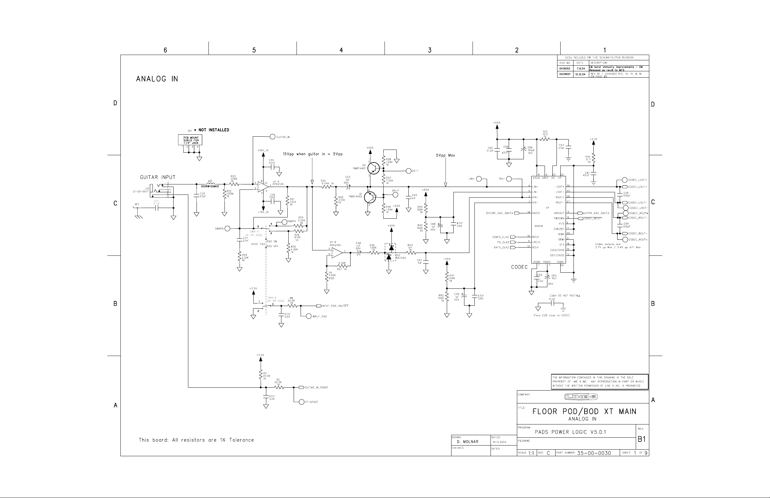
Audio system (see pages 1-2 of the MAIN schematic):
All of the analog audio system is contained in the MAIN PCB. Refer to the Audio System
diagram below for a block diagram of the system.
Guitar Input:
The guitar input (J10) is buffered and amplified by U1A by either a gain of 3 when the
front panel input level is set to NORMAL, or by a gain of 1 when the switch is set to PAD
(= Low Gain). At the same time, U1-A adds high frequency pre-emphasis gain starting at
about 200Hz. U1-A output is spliced into two branches:
- On the upper branch, R34 and R35 attenuate the signal for a +/-2.5 VPP range (@ 5Vpp,
100Hz at guitar input). C43 allows this signal to be DC biased at +2.5V by the ADC
input. Q1 and Q1 clip the signal to a maximum range of 0/5V. The signal drives the left
channel of the ADC section of CODEC U4.
- In the lower branch, U1B adds a gain of 5.32 to the signal. C44 allows this signal to be
DC biased at +2.5V by the ADC input. The double diode D17 limits the maximum signal
swing to a -0.6V /+5.6V range before entering the right channel ADC section of CODEC
U4. Note that the signal on this branch will clip for guitar input level above 0.310 Vpp.
The net result is two signals with a gain difference of 16, each feeding one of the two ADC
inputs. Once these signals are converted and moved into the DSP, the DSP code will monitor
the amplitude of the signals and use one of the two versions most appropriate for the current
input level. The DSP will also apply a de-emphasis filter complementary to the filter function
implemented by U1A. This scheme allows for significantly improving the signal noise and
low-level distortion performance of the ADC.
POD XT LIVE Theory of Operation………Line 6 confidential ……………. Page 1 of 16
Page 33

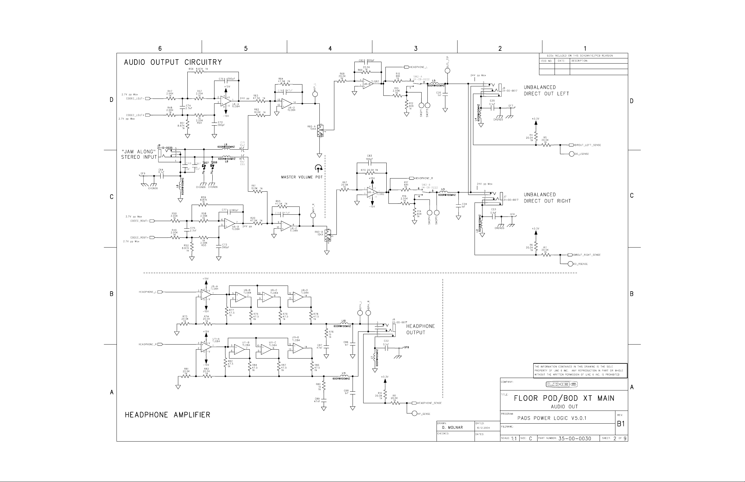
Audio Outputs:
The DAC portion of CODEC U4 sends a stereo pair of differential signals to two low pass
reconstruction filters composed of U6A for the left channel and U6B for the right channel.
Each filter has a cutoff frequency Fc of 20KHz. The two filters then each feed an analog
summation node/buffer (U6-D&C) where the output audio is mixed with the “Jam Along
Input” audio from the AUX IN jack (J9). These two buffers feed the master volume
potentiometer. (Note: This way, the “Jam Along Input” AUX IN level is controlled by the
master volume pot just as the main system audio). The master volume pot feeds the output
buffer stage (U8B for LEFT and U8A for RIGHT). The output of each output buffer stage is
passed through a resistor network and switch that controls the output level for “LINE” level
or “AMP” level. For the “LINE” level the output buffer merely feeds a 681 ohm resistor
(R15 for LEFT and R17 for RIGHT). For the “AMP” level, the output buffer feeds a resistor
divider (R12&R13 for LEFT and R14&R16 for right) which cuts the level by a gain of .091.
The output buffers U8A and U8B also feed the headphone amplifier (U9 for left and U11 for
right).
POD XT LIVE Theory of Operation………Line 6 confidential ……………. Page 2 of 16
Page 34

J6
J7
J6
Hz
Gain from each input
4.435
Reconstruction Low Pass Filter
0 20K
Master
Volume
Pot
Left -
Left -
CLipping
Switch
Line/Amp
gain = 1.0
U6-D
U6-A
Q1 & Q2
Unbalanced Out L
gain = .091
U8-B
DAC
Left +
Left +
+2.5V
U4
CODEC
ADC
Gain Difference: 16
Line
Amp
Right -
Right -
D17
CLipping
U6-C
U6-B
Unbalanced Out R
gain = 1.0
Right +
Right +
+2.5V
gain = .091
U8-A
To DSP
Headphone Output
U9
U11
gain = 5.32
U1-B
Switch
Input Pad
Pad Gain = 1
Normal Gain = 3
"Jam Along" Input
(AUX IN)
J9
POD XT LIVE AUDIO SUBSYSTEM
Gain
2.5
Pre-Emphasis Filter
gain = 0.332
Hz
U1-A
0 200 20K
1
Guitar Input
J10
POD XT LIVE Theory of Operation………Line 6 confidential ……………. Page 3 of 16
Page 35

POD XT LIVE Audio Characteristics:
1) Audio Inputs Max Level:
- Guitar Input max Level in normal mode:
From DC to 200 Hz = 5.0 Vpp, at 1KHz = 4.0 Vpp, at 2KHz = 3.0 Vpp, at 10KHz =
2.0 Vpp, at 20 KHz = 2.0 Vpp
- Guitar Input max Level in pad mode:
From DC to 200 Hz =15.0 Vpp, at 1KHz = 12.0 Vpp, at 2KHz = 9.0 Vpp, at 10KHz =
6.0 Vpp, at 20 KHz = 6.0 Vpp
- Jam Along Input (Aux IN): 5.3Vpp
2) Inputs / Outputs nominal impedance:
- Guitar in nominal input impedance: 1Meg Ohm (for both input PAD ON and PAD
OFF)
- Output ¼” jack Unbalanced nominal output impedance: Stereo = 681 Ohm
- Jam Along Input (Aux IN): 10K Ohm
3) Output signal levels:
Test condition A: Test mode, Guitar input = 1.0Vpp= -9.03dBV, 200Hz
- ¼”Jack Unbalanced Out Left and Right Level for test condition A: 3.8 Vpp =2.56dBV
- Headphone out Level (either side) for test condition A (no load) = 7.7 Vpp = +8.7 dBV
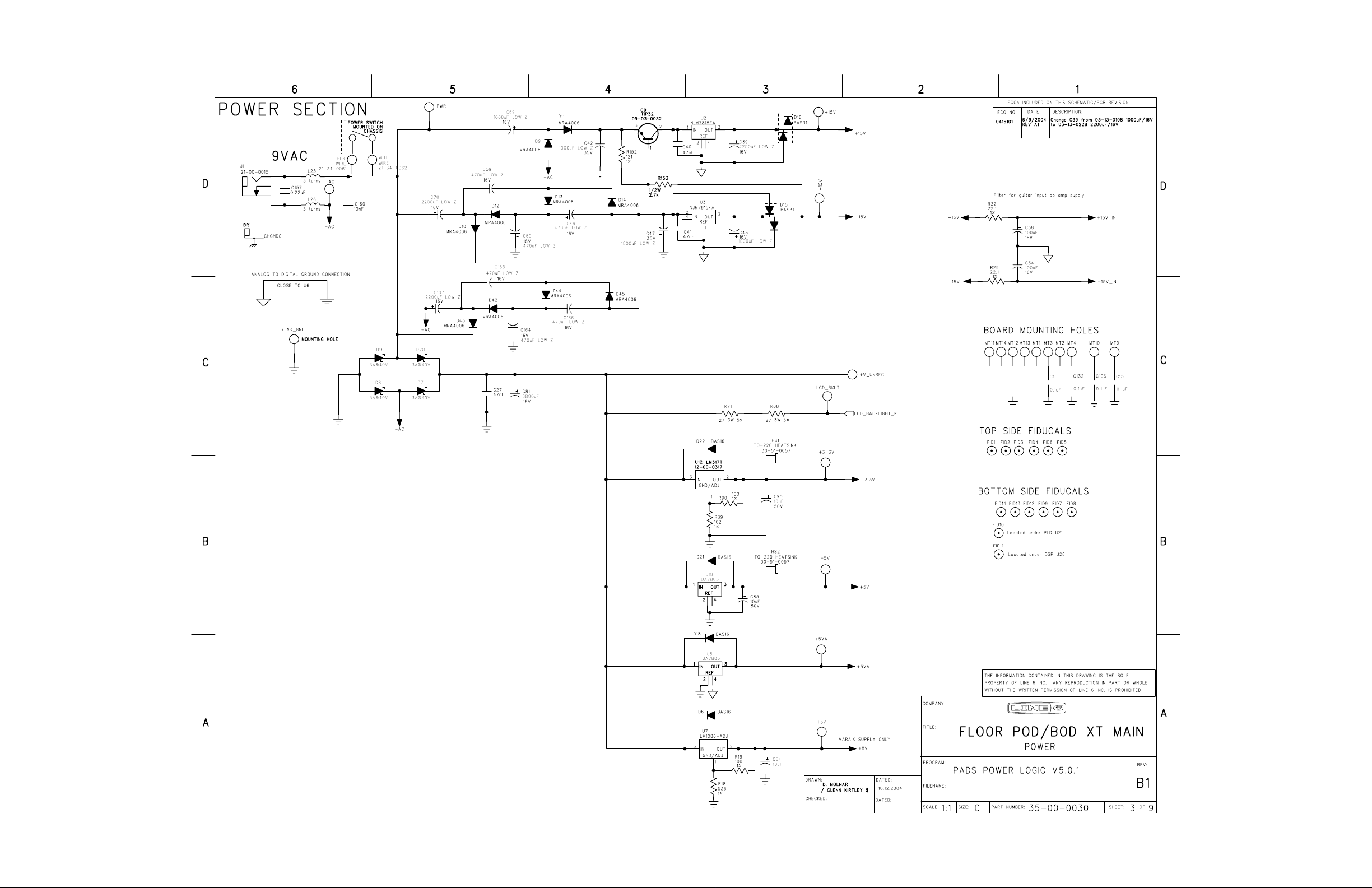
Power supply (page 3 of MAIN schematic):
Refer to the SUPPLY SYSTEM FLOWCHART diagram below.
The POD XT LIVE uses the same external step-down transformer as the POD XT and BASS
POD XT. This transformer supplies 9 VAC to the POD XT LIVE. The 9 VAC is split into
three branches:
- On the +15V branch, the 9VAC is rectified and voltage doubled to approximately +20VDC
with respect to ground by C69, D9, D11, and C42. The transistor Q9 with R152 and R153
acts as a delay such that the +15V supply rail will not come up until the –15V supply rail is
stable. This delay helps reduce the audio thump that may otherwise occur when the unit is
turned ON. Voltage regulator U2 takes +20VDC and produces the +15V rail.
- The –15V branch is a bit more complicated
Since the +AC net is positively offset with respect to ground due to the full-wave rectifier,
a simple voltage “doubler” is not adequate to get the approximate +9V to a value less than
–15VDC. Therefore, the voltage is simply doubled, (C70, D10, C59, D12 and C60) giving
around –10V, and then it is doubled again to produce around –20V by D13, C49, D14 and
C47. In order to help insure symmetrical current draw from the external transformer and at
the same time provide adequate current output of the –15V rail, a second voltage
“quadrupler” is used in parallel and out-of-phase with the other “quadrupler” just
described. This second multiplier consists of components C107, D43, D42, C165, C164,
D44, C166, and D45. Its output is also around –20VDC, but it draws current during the
negative going AC peak.
POD XT LIVE Theory of Operation………Line 6 confidential ……………. Page 4 of 16
Page 36

- The third branch of the 9VAC feeds a full wave bridge rectifier (D7, D8, D19, and D20).
The output of this rectifier is smoothed to around +10VDC mostly by C81. This +10VDC
output is labeled +V_UNREG on the schematic.
- The +V_UNREG is current limited by two 27 ohm 3W resistors and sent to supply the
backlight for the LCD module. Since the LCD backlight supply is not regulated the
LCD backlight intensity my vary slightly with the AC main voltage.
- The +V_UNREG is regulated by adjustable regulator U12 down to +3.3V (digital
supply).
- The +V_UNREG is regulated down to +5V by U10 for the +5V digital supply.
- The +V_UNREG is regulated down to +5V by U5 for the +5V analog supply for the
Codec and immediate circuitry.
- The +V_UNREG is regulated down to +8V by the adjustable regulator U7 for the
Variax supply that is sent out the RJ-45 jack on the rear panel. Note that care has been
taken to assure that shorting the contacts of the RJ-45 jack (and thus short circuiting the
+8V Variax supply) does not damage the POD XT LIVE in any capacity.
The +15V and –15V rails are further filtered by the R32/C38 and R29/C34 networks to
generate the +15V_IN and –15V_IN which are used to supply a very clean power supply for
the input op amp U1 for the guitar input.
Without special care, a 1KHz audio tone may appear on the audio signals when the USB
connection is used and a ground loop is present between the host PC and the audio system. To
avoid this problem, the USB section has its own 3.3V supply (+3.3V_USB) made of Q8 and its
associated circuitry, and an insulation resistance (R121) between the digital ground and the
USB ground (see page 4 of the Main PCB). With this circuit, the 3.3V_USB current is derived
from the +5V supply and the +3.3V is only used as a voltage reference.
POD XT LIVE Theory of Operation………Line 6 confidential ……………. Page 5 of 16
Page 37

+3.3V_USB
USB Section
Supply
USB
+15V_IN
Low
Pass
+15V
+15V
DELAY
Regulator
Op Amp
To: Audio Input
Filter
R32, C38
Op Amps,
To: Audio Output
Headphones, etc...
U2
Q9
-15V_IN
Low
Pass
-15V
-15V
Filter
R29, C34
U3
Regulator
LCD BACKLIGHT
Supply
R71 R88
+3.3V
reference
3.3V Digital Supply
DSP, PLD, SDRAM,
FLASH, etc...
U12
+3.3V
Regulator
Regulator
Q8
5V Digital Supply:
MCU U17, MIDI I/F
+5V
R21
LEDs, POTs, LCD,
AES RCVR/SRC U20, etc...
5V Analog Supply
for Analog Circuitry
U10
Regulator
+5V
Regulator
U5
Variax Supply on
RJ-45 Jack
U7
+8V
Regulator
Digital to Analog Ground Connection
and
D9, D11, C69, C42
Voltage Doubler
Positive Rectifier
POD XT LIVE POWER SUPPLY BLOCK DIAGRAM
and
D10, D12, D13, D14,
C70, C59, C60, C49,
D43, D42, D44, D45,
Voltage Multiplier
Negative Rectifier
9V AC IN
J1
C107, C164, C166
Full
Wave
Bridge
Rectifier
C81
D19
C27
D20D8D7
POD XT LIVE Theory of Operation………Line 6 confidential ……………. Page 6 of 16
Page 38

Input / Output System and Control:
The following Input and Output (I/O) signals control the POD XT LIVE operation and system
mode.
GUITAR_IN_SENSE (MAIN PCB):
The status of the Guitar Input Jack is read from the GUITAR_IN_SENSE line by I/O pin 78 of
the DSP U26. It is high when a jack is plugged in the guitar input and low otherwise.
When this signal is read low (= no jack plugged in), and the Variax input is unplugged, the
DSP mutes the audio signal path in order to keep the noise on the audio outputs at a minimum
DIROUT LEFT_SENSE and DIROUT RIGHT_SENSE (MAIN PCB):
The status of the Direct Output Jacks is read from the DIROUT LEFT_SENSE and DIROUT
RIGHT_SENSE lines by I/O pin 199 and 201 of the DSP U26. Each line is high when the
corresponding jack is plugged in, and low otherwise. Currently the state of these lines has no
effect on the operation of the unit.
HEADPHONE_SENSE (HEADPHONE OUTPUT PCB):
The status of the Headphone output Jack is read from the HEADPHONE_SENSE line by I/O
pin 79 of the DSP U26. It is high when a jack is plugged in the headphone output and low
otherwise. Whenever headphones are plugged in, the DSP is set to “STUDIO DIRECT” mode.
User Interface Potentiometers and Pedals (MAIN PCB):
The POD XT Live has six user interface potentiometers, a variable position pedal, and an
external expression pedal input. The pots and pedals provide a voltage from 0 to 5Vdc. These
voltages are digitized by the 12-bit resolution ADC (U31). This ADC sends the results over a
digital serial stream to the MCU (U17) on the SPI_DATA_MISO line clocked and gated by the
SPI_CLK and SPI_AD_CS* lines.
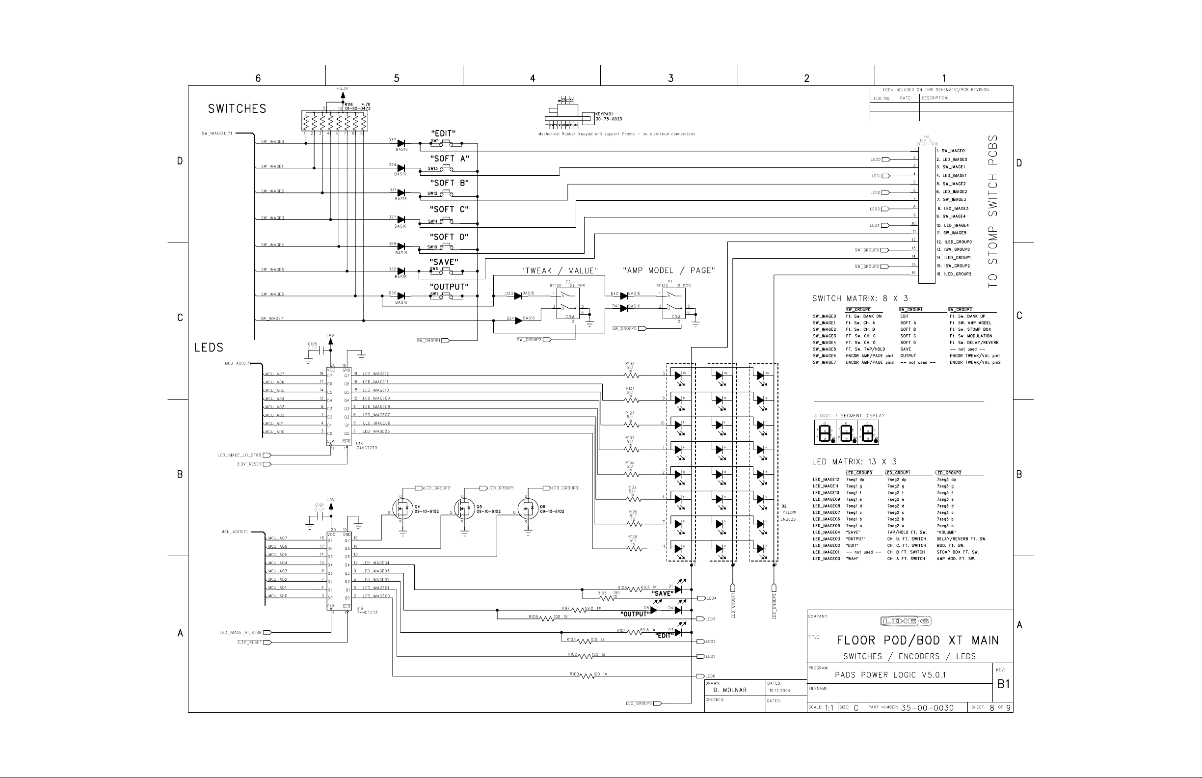
User Interface LEDs / Seven Segment Display (MAIN PCB, SWITCH PCB):
All of the user interface LEDs and seven segment display are grouped in a 3 X 13 multiplexed
matrix under control of the MCU (U17). The LED_IMAGE00…LED_IMAGE12 lines drive
the matrix rows (via drivers U16 and U18). The LED_GROUP0*…LED_GROUP1* lines
drive the matrix columns using FET transistors Q4, Q5, and Q6 to sink the column current.
Under software control, only one LED group line is active at a time. For each LED group a
different LED image is presented in the LED_IMAGExx lines. This matrix multiplexing
happens so fast that the eye perceives all of the LEDs on at the same time. The LED matrix
chart is presented on the MAIN schematic page 8. Most of the LEDs including the LED seven
segment display are on page 8 of the MAIN schematic. Some of the LEDs go off board to the
two halves of the SWITCH PCB via a ribbon cable that connects to H4 of the MAIN PCB.
User Interface Switches and encoders (MAIN PCB, SWITCH PCB):
All of the user interface’s switches and two encoders are read using an 8 by 3 multiplexing
matrix. The 8 switch matrix rows are read by the MCU (U17) using the lines
SW_IMAGE0…SW_IMAGE7 via the PLD (U21). The MCU selects which group of 8
switches (or encoder) to read using the SW_GROUP0*…SW_GROUP2* lines. The two
encoders are each different – E1 has 12 steps and E2 has 24 steps.
POD XT LIVE Theory of Operation………Line 6 confidential ……………. Page 7 of 16
Page 39

User Interface LCD (MAIN PCB):
The LCD module is written to and read from through the MCU’s main bus MCU_AD[0:7].
The MCU firmware can adjust the contrast of the LCD by varying the duty cycle of a 1KHz
pulse generated on the LCD_CONTRAST_PULSE line. This pulse is filtered and summed
with a minus 5V supply available at pin 4 of the LCD module. This results in an adjustable
negative to positive DC voltage at the contrast control input of the LCD (pin3).
The backlight LED array is supplied on pin 20 of the LCD module. Two 27 ohm resistors in
series (R71 and R88) set the backlight brightness.
POD XT LIVE Theory of Operation………Line 6 confidential ……………. Page 8 of 16
Page 40

Clock system (Pages 4,5, and 9 of the MAIN PCB):
The drawing below details the clock distribution structure of the POD XT LIVE:
Rx
Audio
Digital
Variax
Input Clock
MCU
U17
USB Controller
FS_CLK
CLK_6MHZ
U25
USB_64FS_CLK
USB_256FS_CLK
U4
CODEC 1
256FS_CLK = 10MHz
64FS_CLK = 2.5MHz
Sample
Output Clocks
U20: SRC & AES IN
FS_CLK = 39.0625KHz
USB Clocks
Internal Clocks
Divide By 64
Rate
Converter
U26
DSP
VARIAX_RECOVERED_256FS_CLK
Variax Recoverd Clock
Divide By 2
CLK_30MHZ CLK_15MHZ
Divide By 5
Internal Clock
Divide By 3
Divide By 4
Inside PLD U21
Y1
30 MHZ
The 30 MHz Oscillator Y1 (via the PLD) generates the bulk of the on board system clocks.
PLD U21 derives several clocks from Y1 including: CLK_15MHZ for the MCU U17,
POD XT LIVE Theory of Operation………Line 6 confidential ……………. Page 9 of 16
Page 41

CLK_6MHZ for the USB controller U25, and the three internal digital audio clocks. The three
internal digital audio clocks are 256FS_CLK (10MHz), 64FS_CLK (2.5 MHz digital audio bit
clock), and FS_CLK (39.0625 KHz sample rate). These internal digital audio clocks are used
by the DSP, the CODECs, and the Internal side of the Sample Rate Converter IC for the
Variax receiver. When the USB controller is active and connected to a PC with an audio
application, the three clocks 256FS_CLK, 64FS_CLK, and FS_CLK are generated by the USB
controller (see above diagram). When the Variax is plugged in the
VARIAX_RECOVERED_256FS_CLK is used in place of the internal clock. When both the
Variax and USB are active, the recovered Variax clock is NOT used and instead the Variax
digital audio signal is passed through a sample rate converter and synchronized to the USB
clocks.
POD XT LIVE Theory of Operation………Line 6 confidential ……………. Page 10 of 16
Page 42

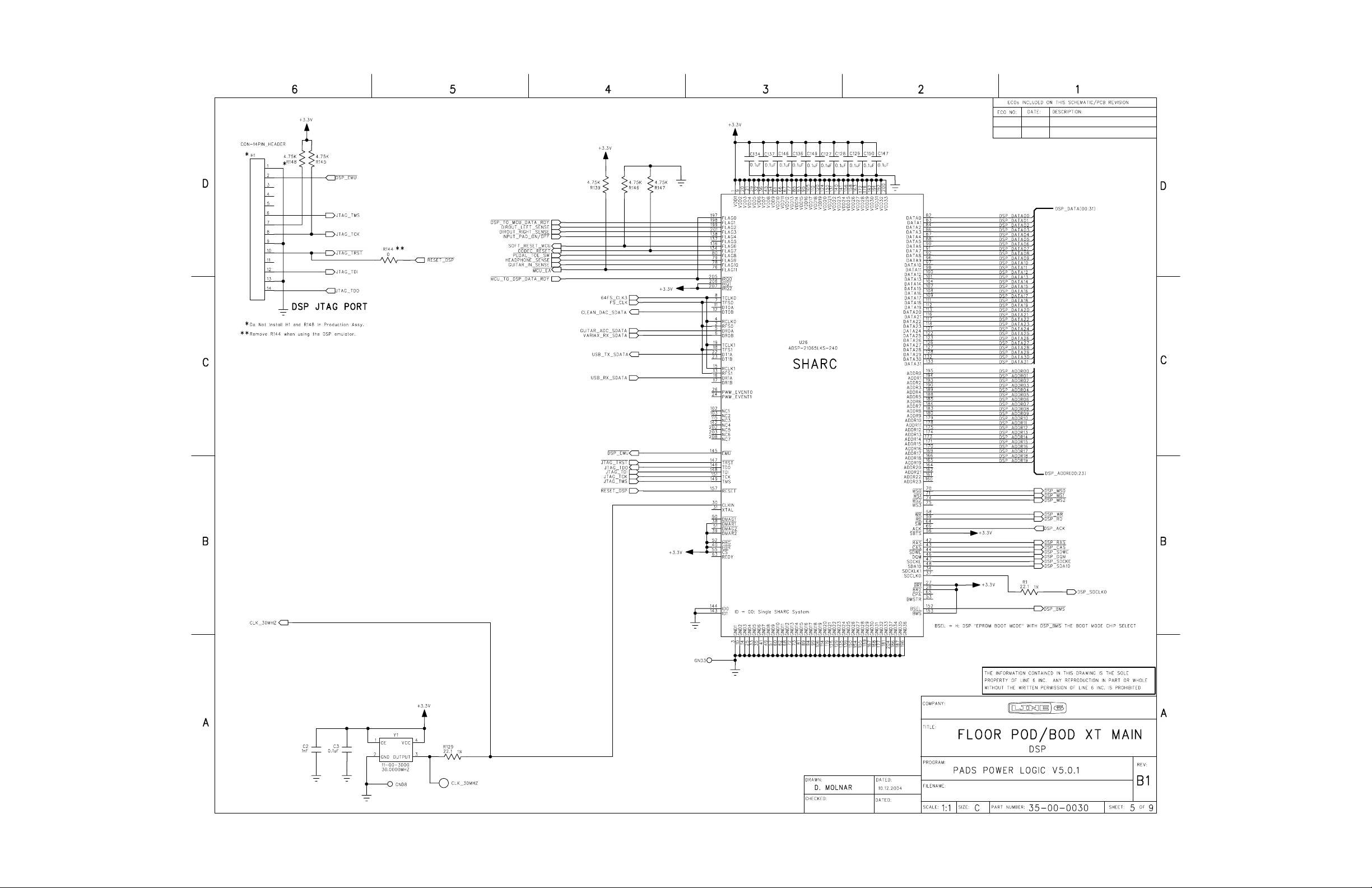
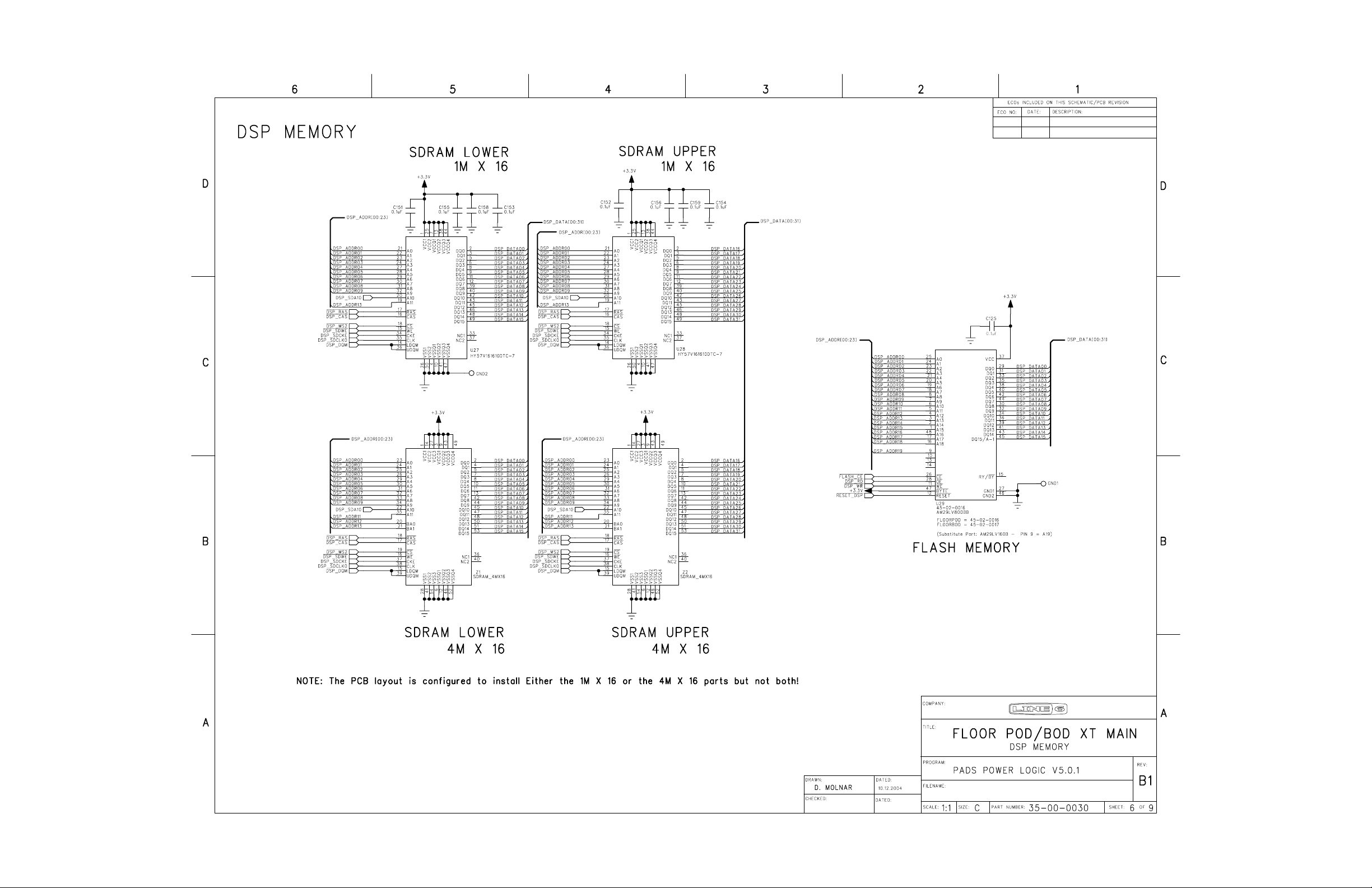
Bus system:
The drawing below details the interconnecting busses between the subsystems of the POD XT
LIVE:
1M X 16 U28
4M X 16 Z1
1M X 16 U27
4M X 16 Z2
Only the 1M X 16 or
4M X 16 SDRAMs
are installed at a
time.
SHARC DSP
U26
0..31
16..31
DSP_DATA[00..31]
0..15
SDRAM LO
SDRAM HI
\MCU_TO_DSP_DATA_RDY
\DSP_TO_MCU_DATA_RDY
P87C51MB2A
OTP MCU
U17
0..7
8 bit latch
w/busy flag
\MCU_TO_USB_DATA_RDY
\USB_TO_MCU_DATA_RDY
0..15
0..7
8 bit latch
w/busy flag
MCUAD[0..7]
FLASH
U29
INTERFACE
INSIDE PLD
w/busy flag
w/busy flag
SRAM
U14
BUS
U21
8 bit latch
8 bit latch
USB_LOCAL_D[0..7]
TAS1020A
Controller
I2C BUS
ISP
Cable
I / F
H2
for PLD
USB
JACK
USB
U25
EEPROM
U23
SECURE
MEM
U24
8 Ch. ADC
U31
...
MIDI
Variax
MIDI
POTs
LCDLEDs
Switches
and
Encoders
POD XT LIVE Theory of Operation………Line 6 confidential ……………. Page 11 of 16
Page 43

The Micro-controller (MCU U17) is the master host controller for the POD XT LIVE. Its data
bus (MCU_AD[0..7]) interfaces locally to 128K X 8 of SRAM (U14). All of the user interface
components: LCD, LEDs, the Switches, and Encoders are connected to this bus either directly
to this bus (LCD), through drivers (LEDs), or via a bus buffer (switches) in the PLD (U21)
(pages 7 and 8 of main schematic). This bus is also bridged to both the DSP and USB
subsystems via bidirectional latches inside the PLD U21. All address decoding for the MCU is
performed inside the PLD. (Note: The above diagram does not show the address bus and
control lines).
The MCU U17 is a One Time Programmable microcontroller (OTP). It contains the BOOT
CODE ROM for the POD-XT PRO system as well as some internal SRAM. VERY
IMPORTANT - This chip must be programmed like and EPROM before it can be used in the
POD XT LIVE system.
The interface between the MCU and DSP is located inside the PLD U21. If the MCU wishes
to send a byte to the DSP, it writes a byte to the MCU-to-DSP latch inside the PLD. Writing
this byte causes a busy flag to become asserted (MCU_TO_DSP_DATA_RDY*). When this
flag is asserted, the DSP receives an interrupt, which tells the DSP to read the byte from the
MCU-to-DSP latch. The MCU_TO_DSP_DATA_RDY* flag is deasserted when the DSP
reads the MCU-to-DSP latch. The MCU polls the MCU_TO_DSP_DATA_RDY* line and
cannot write another byte until this line is deasserted. This same process works for the
DSP_TO_MCU_DATA_RDY* for sending bytes from the DSP to the MCU.
The DSP local bus (DSP_DATA[00..31] is a 32 bit bus that interfaces 32 bit wide SDRAM in
2 1MX16 chips U27 and U28 (note that you can substitute 4MX16 chips in the overlapping IC
locations Z1 and Z2 but this is not currently used) and the FLASH memory U1 to the DSP.
This bus is bridged to the MCU bus via the bidirectional latch inside the PLD U21 described in
the paragraph above.
The interface between the MCU and USB subsystem is also located inside the PLD U21. This
interface bridge is identical to the interface between the MCU and DSP subsystem. The USB
local bus (USB_LOCAL_D[0..7]) is only used to bridge the USB subsystem to the MCU bus
via the bidirectional latch inside the PLD. All peripherals in the USB subsystem are interfaced
via an I2C (Inter IC) bus. The I2C bus is a 2 wire bus used for local low speed serial
communication between all I2C compatible chips on a pc board. The I2C bus connects the
EEPROM U23 and Secure Memory U24 to the TAS1020A USB controller U25.
POD XT LIVE Theory of Operation………Line 6 confidential ……………. Page 12 of 16
Page 44

Boot Up Sequence:
The POD XT LIVE has quite a sophisticated boot up sequence, which is outlined below:
1. On power up, the reset IC U22 generates an active HIGH reset. This is the master reset
for the entire POD XT LIVE system.
2. When this “master reset” line is deasserted, the MCU polls the MCU_EA* during the
falling edge of its reset. This line will be HIGH causing the MCU to execute code from
its internal OTP ROM.
3. The MCU will deassert the RESET_DSP* line (via the PLD) thus taking both the DSP
and USB controller out of reset (see next section below for USB reset process).
4. The MCU will then send the DSP’s boot code to the DSP via the MCU to DSP bridge
inside the PLD. This DSP boot code is stored in the MCU’s OTP ROM during power
down.
5. Once the DSP has received all of its boot code from the MCU, it loads its runtime code
from the FLASH memory located on its data bus and begins execution.
6. The DSP will then send the MCU’s runtime code to the MCU where the MCU will
store it in the volatile SRAM U14.
7. Once all of the MCU runtime code is received by the MCU, the DSP will RESET the
MCU. The DSP drives MCU_EA* to the LOW state, then asserts SOFT_RESET_MCU
to reset the MCU. After the reset period, the DSP deasserts SOFT_RESET_MCU and
drives MCU_EA* HIGH again. The MCU will now begin to run its runtime code from
the external SRAM U14. The MCU uses the state of the MCU_EA* line during the
falling edge of its reset line to determine if it will run its OTP ROM boot code or
execute code externally from the SRAM. This time it runs code externally because the
DSP held the MCU_EA* low during the falling edge of its reset.
The USB subsytem is reset by the active low signal RESET_DSP*. This signal is a product of
the master reset IC so the USB subsystem is reset only during a board power up.
1. When reset is removed from the USB controller U25, its special internal firmware
checks the EEPROM U23 to see if it contains the USB controller runtime code. If the
EEPROM is blank then the USB controller attempts to load its code via USB jack. If
the USB controller is able to load code from the USB jack it loads this code into the
EEPROM (This is how the POD XT LIVE tester loads code for the USB into the
board.)
2. Once there is valid code in the EEPROM and it is loaded into the USB controller, the
USB controller will begin executing this code.
3. Upon executing its runtime code, the USB controller checks the secure memory U8 to
see if it is sealed. If it is sealed then USB encryption is enabled. (The secure memory
is “Sealed” during the production test process. The “sealing” process ensures
appropriate serial numbers are written to the USB encryption subsystem)
POD XT LIVE Theory of Operation………Line 6 confidential ……………. Page 13 of 16
Page 45

Troubleshooting:
This section outlines some common problems that may be encountered when troubleshooting a
POD XT LIVE.
1. Since the USB jack is located next to the RJ-45 jack it was noticed that one can very
easily plug the USB cable into the RJ-45 jack. Now, of course, this will not work but
the shield of the USB plug will short all 8 lines of the RJ-45 jack. Special care was
taken when designing the circuitry of the RJ-45 jack such that shorting the power and
ground will not damage the board. The added circuitry should provide adequate
protection. If a board is damaged by inserting the USB plug into the RJ-45 jack please
notify engineering.
2. The FLASH memory on the POD XT LIVE is updated every seven seconds with any
setting changes (eg. MIDI channel, LCD contrast, knob change, etc…). This means
that if the POD XT LIVE is powered down in less then seven seconds after a setting is
changed then the item will not be stored correctly in the FLASH memory. When the
POD XT LIVE is powered back on, its previous setting will be restored.
3. The board powers up and the LCD backlight turns on but the LCD is blank or garbled –
if the rest of the system seems to be functioning correctly (TAP tempo light flashes,
buttons work, audio passes, etc.) then the LCD reset circuitry may be at fault (Q3) or
the LCD module itself may be defective.
4. If the LCD’s backlight does not turn on but the rest of the system work properly - check
that the 27R resistors on LCD_BACKLIGHT_K are the correct value or are not open
circuit. The LCD module’s backlight itself may be defective – in this case the only fix
is to replace the LCD module.
5. The board powers up but the LCD reports “ERROR CODE 2” or “ERROR CODE 1”.
This means that the FLASH memory is empty or invalid. “ERROR CODE 1” means
that the MCU runtime code that is stored in the DSP’s FLASH is invalid. “ERROR
CODE 2” means that the DSP runtime code that is stored in FLASH is invalid. See
previous section on POWER UP SEQUENCE for more information. If either of these
messages are displayed, then try reprogramming the FLASH memory. If it fails again,
then check for faulty soldering on the DSP’s bus or MCU bus (see section on BUS
SUBSYSTEM for more information). Note also that a faulty device on either of these
busses may be at fault.
6. The board is powered up but the LCD is blank and the rest of the system is frozen.
First, make sure that the MCU is installed. Second, try another MCU. Third, check for
faulty soldering on the MCU bus (especially the MCU socket S1). Fourth, make sure
the PLD is programmed properly. This can only be verified with the PLD
programming cable and accompanying PC software. One other way to verify that the
PLD is ok is to check for all of the clocks that the PLD drives (the clocks can be found
on an number of test points throughout the board). Fifth, check the master oscillator Y3
to see if it is generating the 30MHz clock. Sixth, check for faulty components on the
MCU bus side. Finally, check that a proper reset is generated by the reset IC U22.
7. The board powers up, the LCD is displaying the correct items, the buttons, knobs, and
LEDs work, but there is NO AUDIO. First check that the pedal is in the toe down
position and that there is no external expression pedal plugged in. Second, check that
the Variax input is unplugged because this will override the guitar input. Third, check
POD XT LIVE Theory of Operation………Line 6 confidential ……………. Page 14 of 16
Page 46

that the signal GUITAR_IN_SENSE is HIGH (HIGH means that a jack is plugged into
the POD XT LIVE’s guitar input.). If this signal is not HIGH then the guitar in jack
J10 or the support circuitry for the sense line is faulty. If the system thinks that a plug is
not plugged into the guitar jack it will automatically mute the audio. Fourth, check the
audio input circuitry and make sure audio makes it through the input op-amp U1 all the
way to the CODEC (U4) inputs. Third, make sure that the codec has the appropriate
clocks driving it (See section CLOCK SYSTEM above). Fifth, check the audio path
from the output of the codec to the unbalanced direct outs and the headphone circuitry.
Sixth, the audio is correct all the way to the codec and the clocks are correct then it is
possible that the DSP or an item on its bus is malfunctioning. At this point check for
faulty soldering on the DSP or other items on its bus.
8. The buttons and encoders work but the pots do not. First power down and then power
up in test mode (Press the SOFT D button under the LCD on power up). If the pots fail
in test mode check the ADC U31 and the clocks and\or signals going between this ADC
and the MCU.
9. The board seems to be working properly but the LED’s do not work. First power down
and then power up in test mode (Press the SOFT D button under the LCD on power
up). If the LEDs fail in test mode check the U16 and U18 latches as well as FETs Q4,
Q5, and Q6. If the LEDs under the UI keypad buttons work but the stomp switch LEDs
do not then check the ribbon cable between the MAIN PCB and the SWITCH PCB
halves and also check the SWITCH PCB halves themselves.
10. The board seems to be working but the buttons and encoders do not work. First power
down and then power up in test mode (Press the SOFT D button under the LCD on
power up). If the buttons and encoders do not work in test mode check anything in the
SW_IMAGE[0:7] bus and MCU_AD[0:7] bus, resistor pack R116, and any of the
switch matrix diodes (see MAIN schematic page 8).
11. The board is running but the USB does not work. Check for faulty soldering on the
USB controller U25 as well as the EEPROM U23 and secure memory U24 and pull-up
resistors R124 and R130. Check the special USB supply isolation circuit (See
schematic page 4). Finally check for faulty components in the USB subsystem.
12. The board is running but the VARIAX interface does not work: Check the AES
Receiver/SRC U20 and check the Variax MIDI transceiver U30.
13. The board is running but the MIDI interface does not work. Check the MIDI I/O
section for faulty soldering (See schematic page 9). Check for faulty soldering on the
MCU U17, the PLD U21, etc.
14. The unit works ok except for the pedal:
?? First: Make sure that the pedal is calibrated properly – you can do this by powering
up with the “BANK UP” stomp switch held. This puts the unit into a special pedal
calibration test mode. The LCD will display several fields of numbers. Press the
“AMP ON/OFF” stomp switch to reset the calibration. Move the pedal to the heel
position. Move the pedal to the toe position and depress the pedal’s toe switch.
Move the pedal back to the heel position. When in the heel position now the “7
MAPPED xxx” number on the LCD should read 0. Move the pedal back to the toe
down position(you do not have to depress the toe switch). With the pedal now in
the toe down position the “7 MAPPED xxx” number should read 127. You should
POD XT LIVE Theory of Operation………Line 6 confidential ……………. Page 15 of 16
Page 47

also see this number sweep from 0 to 127 as the pedal is moved from heel down to
toe down.
?? Second: If the pedal fails to calibrate properly you should check the metal lance
that moves above the IR sensor. The long part of the lance should be at a 90 degree
angle to the plane of the pedal. If the long part of the lance is not at a 90 degree
angle to the plane of the pedal you may try adjusting it accordingly.
?? Third: After trying all of the above - there may be a problem with the IR emitter or
IR phototransistor on the PEDAL PCB. Also, the interconnecting cable between the
MAIN PCB and PEDAL PCB may be defective.
POD XT LIVE Theory of Operation………Line 6 confidential ……………. Page 16 of 16
Page 48

Line 6 Manufacturing
Floorpod XT Assembly Instructions Rev B
Document # L6D000017
LEFT
FRONT
BACK
RIGHT
Forward and Notes
The information in this booklet applies the Floorpod XT (also known as: PODxt LIVE). It is
suggested that the steps for assembly follow the order presented in these instructions.
These instructions deal with the assembling the major sub-assemblies, the final product, and
quality/inspection considerations. See also the Related Electrical assembly documentation, for
major considerations in assembling the electrical components of the PCBs (through the soldering
process and preparation of the board for addition of custom components).
A note on the text: the illustrations in this book are for reference only. In some cases, color and
geometry of illustrations may not accurately reflect the color or exact geometry of actual parts.
?? Unless otherwise noted, all dimensions are in inches.
?? Part identifying notes are in this format: Description (Part Number)
?? Drawings are not to scale.
?? Torque value tolerance +/- .5 in.-lbs. Do not over tighten any components.
?? For clarity, not all component details are shown. This is especially true with respect to
cable assemblies. They are often omitted from views to provide a clearer picture of the
material discussed. Do not be confused by the absence (or unexpected presence) of any
component in the illustrations in this book.
Confidential Page 1 of 41 9/7/2004
Page 49

Line 6 Manufacturing
Floorpod XT Assembly Instructions Rev B
Document # L6D000017
Revision Comment Sheet
Revision Changes
A N/A
B Miscellaneous typographical errors corrected
Step 3. Added 1 each pedal support bracket and 2 each nylon washers
Added exploded assembly view to Figure 1
Fastener torque values changed
Step 4. Fastener torque values changed
Step 5. Fastener torque values changed
Step 6. Fastener torque values changed
Added 2 each steel washers
Figure 1 revised
Step 8. Instructions Updated with correct part numbers.
Step 9. Fastener torque values changed
Step 10. Added Lens inspection note
Step 11. Fastener torque values changed
Step 15. Fastener torque values changed
Step 17. Part quantity changed
Fastener torque values changed
Step 19. UPC/Serial Number label part number corrected.
Confidential Page 2 of 41 9/7/2004
Page 50

Line 6 Manufacturing
Please notice the placement
should be placed close to the
Floorpod XT Assembly Instructions Rev B
Document # L6D000017
STEP 1. PEDAL SUB-ASSEMBLY
P/N required:
1 each 30-75-0002 Foot Rubber
1 each 30-51-0181 Pedal
2 each 30-75-0011 Rubber Pedal stop
1 each 30-75-0007 Pedal Stop Foam Rubber
1.1 Install Foot Rubber onto the Pedal
1.1.1. Install FOOT RUBBER to the PEDAL top surface. Press firmly. The Pedal shall
be clean and dry. DO NOT BEND THE LANCE.
Pedal Sub-Assembly
To complete the Pedal sub-assembly the following must be attached to the Pedal. Each
rubber part has pressure sensitive adhesive on the side to be attached to the Pedal.
2 each Rubber Pedal Stops
1 each Pedal Stop Foam Rubber
1 each Foot Rubber
of the Pedal Stops between
the small rectangular
cutouts. Also make sure
that they as close to the
Pedal edge as possible.
Confidential Page 3 of 41 9/7/2004
The Foam Rubber Stop
bottom edge of the Pedal as
Page 51

Line 6 Manufacturing
Floorpod XT Assembly Instructions Rev B
Document # L6D000017
STEP 2. PEDAL PCBA and PEDAL SWITCH PCBA
P/N required:
1 each 35-00-0032 Switch PCB (break away part)
3 each 30-51-0078 Tactile Domes
1 each Scotch Transparent Tape 144 or equivalent
2.1. To complete this sub-assembly place three (3) Tactile Domes aligned on top of each
other (make sure there are exactly 3 Tactile Domes used, they are thin and easily misscounted) and tape them to the Pedal Switch PCB so that the feet of the bottom Tactile
Dome rest on the conductive pads.
Break away switch PCB
Tactile Domes
Clear tape used to hold
Tactile Domes in place for
assembly. Please notice the
alignment of Tactile Domes
and placement of Tape.
Confidential Page 4 of 41 9/7/2004
Page 52

Line 6 Manufacturing
Nylon Washers
work if the insulator is not on the correct
chassis
Floorpod XT Assembly Instructions Rev B
Document # L6D000017
2.2. Pedal Switch PCB to Chassis Assembly
P/N required:
2 each 30-03-0013 Nylon Washers .5 x .170 x .04 thick
2 each 30-15-0005 Round Aluminum Spacers 1/4 OD X .166 ID X .460
1 each 30-15-0006 Insulator Plastic .17 OD X .156 ID X .460 LNG
PEM for
Pedal PCBA
Back surface of the Chassis
30-03-0013
Round Plastic Insulator
IMPORTANT: Note the location of the
insulator. The pedal activation will not
stud.
PCB breakaway tabs point to BACK of the
Pedal Switch PCB sub-assembly
Round Aluminum Spacers
Confidential Page 5 of 41 9/7/2004
Page 53

Line 6 Manufacturing
Floorpod XT Assembly Instructions Rev B
Document # L6D000017
STEP 3. PEDAL PCBA to CHASSIS Assembly
P/N required:
1 each 50-02-0032 Pedal PCBA
2 each 30-03-0013 Nylon Washer
1 each 30-51-0197 Pedal Support Bracket
1 each 30-00-0043 6-32 x 5/16 Screw with captive star washer
2 each 30-06-0623 6-32 Hex nuts with captive star washer
1 each 30-15-0004 Spacer .13 x.63 OD Nylon Black
3.1. Install Pedal PCBA
3.1.1. Position the PCBA onto the 2 threaded studs
3.1.2. Install 2 each Nylon Washers on to the threaded studs.
3.1.3. Install the Pedal Support Bracket onto the threaded studs. Note: the Bracket has
a FRONT side that must be positioned toward the Chassis Front.
3.1.4. Install 2 each 6-32 nuts onto the threaded studs. Only finger tight.
3.1.5. Install 1 each 6-32 x 5/16 PPH machine screw to secure the PCBA to the standoff.
Only finger tight.
3.1.6. Install Black Nylon Spacer, Black Finishing Washer and Chrome Nut onto ¼” jack
on the BACK of the chassis. See figure 1 on next sheet.
FASTENER TORQUE VALUE = 5-6 in/lbs
3.1.7. Torque screw (30-00-0043) & 2 nuts (30-06-0623).
FASTENER TORQUE VALUE = 10-12 in/lbs
Confidential Page 6 of 41 9/7/2004
Page 54

Line 6 Manufacturing
32 x 5/16 Screw
2 each Nylon Washer
30-51-0197
Floorpod XT Assembly Instructions Rev B
Document # L6D000017
¼” Jack Assembly
1 each Chrome Nut
1 each Black Finishing Washer
1 each Black Nylon Spacer
30-15-0004
2 each Hex Nuts
30-06-0623
1 each Pedal Bracket
30-03-0013
1 each 630-00-0043
Pedal PCBA
Top Chassis
Step 3 - Exploded View
Step 3 – Figure 1
Step 3 Complete
Confidential Page 7 of 41 9/7/2004
Page 55

Line 6 Manufacturing
Floorpod XT Assembly Instructions Rev B
Document # L6D000017
STEP 4. KNOB GUARD INSTALLATION
P/N required:
1 each 30-51-0187 Knob Guard
2 each 30-00-0062 Screw 10-32 X 3/8” with star washer
4.1 Install the KNOB GUARD.
4.1.1. Use 2 each 10-32 x 3/8 PPH machine screws, secure the KNOB GUARD to the
CHASSIS TOP.
FASTENER TORQUE VALUE = 16-20 in-lbs.
TOP VIEW
BOTTOM VIEW
Confidential Page 8 of 41 9/7/2004
Page 56

Line 6 Manufacturing
Floorpod XT Assembly Instructions Rev B
Document # L6D000017
STEP 5. PEDAL BRACKET to CHASSIS ASSEMBLY
P/N required:
1 each 30-51-0180 Chassis Top
1 each 30-51-0046 Pedal Bracket
4 each 30-00-0013 6-32 x.250 PPH Screws
The Pedal Bracket are attached to the under side of the Chassis using the four 6-32 x.250
PPH screws.
FASTENER TORQUE VALUE = 10-12 in-lbs
Screw
30-00-0013
Bracket
30-51-0046
Confidential Page 9 of 41 9/7/2004
Page 57

Line 6 Manufacturing
Floorpod XT Assembly Instructions Rev B
Document # L6D000017
STEP 6. PEDAL ASSEMBLY
The Pedal is attached to the Chassis by using the following parts:
P/N required:
4 each 30-03-0003 STEEL WASHERS ¼ ID ½ OD .030 Thick
2 each 30-03-0007 NYLON SPACERS ¼ ID ½ OD .125 Thick
2 each 30-03-0005 NYLON SPACERS ¼ ID ½ OD .030 Thick
1 each 30-06-0009 1/4-20 LOCKNUT w/ Nylon Insert
1 each 30-00-0012 Socket Head Cap Screws 1/4-20 UNC x 3-1/2
1 each 30-15-0011 SPACER 0.39 DIA X 2.40 LG.
1 each 30-51-0181 PEDAL
1) Pedal lance is carefully guided through
chassis. NOTE:Take special care not to bend
the lance.
2) Pedal mounting lugs are inserted through
these slots.
3) Assemble screw, spacer, washer parts,
and nut in the correct order, as shown in
FIGURE 1 on next sheet.
Confidential Page 10 of 41 9/7/2004
Page 58

Line 6 Manufacturing
C B A A A B C D E
30-51-0011 Spacer
Floorpod XT Assembly Instructions Rev B
Document # L6D000017
STEP 6 PEDAL ASSEMBLY
The Pedal is attached to the Chassis by using the following parts:
Item (SEE FIGURE 1 BELOW)
A 30-03-0003 Steel Washer ¼ ID ½ OD .030 Thick
B 30-03-0007 Nylon Spacer ¼ ID ½ OD .125 Thick
C 30-03-0005 Nylon Spacer ¼ ID ½ OD .030 Thick
D 30-06-0009 1/4-20 Locknut w/ Nylon Insert
E 30-00-0012 Socket Head Cap Screw 1/4-20 UNC x 3-1/2
A
Shown without
FASTENER TORQUE VALUE = 19 in-lbs.
Figure 1, 30-15-0011 Spacer is shown assembled above.
Confidential Page 11 of 41 9/7/2004
Page 59

Line 6 Manufacturing
Floorpod XT Assembly Instructions Rev B
Document # L6D000017
STEP 7. BEZEL INSTALLATION
P/N required:
1 each 30-27-0101 BEZEL
6 each 30-00-4250 #4 x .25 PPH Black sheet metal screw
7.1. Install BEZEL.
7.1.1. Place the BEZEL on the TOP CHASSIS. The bosses on the BEZEL will align
with the TOP CHASSIS holes.
7.1.2. Use 6 each #4 x .25 PPH screws to secure the BEZEL.
FASTENER TORQUE VALUE = 3-4 in-lbs.
Until fully seated against sheet metal.
Confidential Page 12 of 41 9/7/2004
Page 60

Line 6 Manufacturing
-10 -11 -12 -13 -14 -20 -21 -15 -16 -17 -18
Floorpod XT Assembly Instructions Rev B
Document # L6D000017
STEP 8. FOOTSWITCH INSTALLATION
P/N required:
1 each 50-04-0099-10,11,12,13,14,15,16,17,18 Footswitch Assembly with Light pipe
1 each 50-04-0099-20,21 Footswitch Assembly without Light pipe
22 each 30-00-0042 #4 x .375 PPH Black sheet metal screw
8.1. Install Plastic footswitch assemblies into the Top Chassis in the positions shown
below.
8.1.1. 11 each:
2 without Light pipes (BANK UP & BANK DOWN),
9 with Light pipes (AMP, STOMP, MOD, DELAY, A,B,C, D, TAP).
Notes:
1. Refer to drawing 30-27-0099 for the 50-04-0099 Assembly Reference View.
2. Top Chassis silkscreen shows correct position of Footswitch Assemblies.
Confidential Page 13 of 41 9/7/2004
Page 61

Line 6 Manufacturing
Floorpod XT Assembly Instructions Rev B
Document # L6D000017
Bottom feature of Footswitch locks into
front edge of TOP CHASSIS hole
Top Chassis footswitch
Confidential Page 14 of 41 9/7/2004
Page 62

Line 6 Manufacturing
Floorpod XT Assembly Instructions Rev B
Document # L6D000017
Insert the Footswitch assembly into the Chassis hole
Push forward to fully seat against the sheet metal edge
Footswitch Assemblies with Light Pipes will align with the Light Pipe hole.
Confidential Page 15 of 41 9/7/2004
Page 63

Line 6 Manufacturing
Floorpod XT Assembly Instructions Rev B
Document # L6D000017
8.1.2. Use 2 each #4 x 3/8” PPH screw (30-00-0042) to secure each FOOTSWITCH
assembly.
FASTENER TORQUE VALUE = 3-4 in-lbs.
Until fully seated against sheet metal.
Confidential Page 16 of 41 9/7/2004
Page 64

Line 6 Manufacturing
Floorpod XT Assembly Instructions Rev B
Document # L6D000017
STEP 9. FOOTSWITCH PCBA INSTALLATION
P/N required:
1 each 50-02-0033 Switch PCBA (upper row and bottom row)
11 each 30-00-0042 #4 x 3/8 PPH Black sheet metal screw
11 each 30-00-0043 6-32 x 5/16 PPH machine screw with lock washer
1 each 30-15-0023 #6 x .25 x .125 Nylon Spacer
1 each 30-06-0623 Nut hex 6-32 w/captive star washer.
Top switch PCBA
Bottom switch PCBA
Confidential Page 17 of 41 9/7/2004
Page 65

Line 6 Manufacturing
Floorpod XT Assembly Instructions Rev B
Document # L6D000017
9.1 Install Top Footswitch PCBA
9.1.1. Install 1 each Nylon Spacer on the 6-32 threaded stud located near the pedal
PCBA.
Confidential Page 18 of 41 9/7/2004
Page 66

Line 6 Manufacturing
Floorpod XT Assembly Instructions Rev B
Document # L6D000017
9.1.2. Place the PCBA over the stud and spacer and align with the standoffs located near
each FOOTSWITCH.
9.1.3. Install 1 each 6-32 nut (30-06-0623) on the threaded stud.
LEAVE THIS NUT LOOSE.
9.1.4. Install 5 each 6-32 x 5/16 PPH machine screws (30-00-0043).
9.1.5. Install 5 each #4 x .375 (30-00-0042) into the FOOTSWITCH bosses.
P/N 30-00-0042 SCREW TORQUE VALUE = 5-6 in-lbs.
P/N 30-00-0043 SCREW TORQUE VALUE = 10-12 in-lbs.
P/N 30-06-0623 NUT TORQUE VALUE = 10-12 in-lbs.
Confidential Page 19 of 41 9/7/2004
Page 67

Line 6 Manufacturing
Floorpod XT Assembly Instructions Rev B
Document # L6D000017
9.2 Install Lower Footswitch PCBA
9.2.1 Place lower PCBA in position over the footswitch hole locations, and chassis
PCBA standoffs.
9.2.2 Install 6 each 6-32 x 5/16 PPH machine screws (30-00-0043).
Do not fully tighten.
9.2.3 Install 6 each #4 x .375 (30-00-0042) into the FOOTSWITCH bosses.
P/N 30-00-0042 SCREW TORQUE VALUE = 5-6 in-lbs.
P/N 30-00-0043 SCREW TORQUE VALUE = 10-12 in-lbs.
Confidential Page 20 of 41 9/7/2004
Page 68

Line 6 Manufacturing
Floorpod XT Assembly Instructions Rev B
Document # L6D000017
STEP 10. LENS PLACEMENT
P/N required:
1 each 30-27-0105 LENS
10.1. Inspect the LENS for scratches and dust. Use clean, no oil, compressed air OR
lint-free cloth to remove dust as necessary. LENS that is scratched in the view area (see
part drawing) MUST BE REPLACED.
10.1.1. Place LENS over the LED and LCD displays on the MAIN PCBA as shown.
10.1.2. LENS sits on surfaces of the rubber KEYPAD.
The LENS is secured from the top by contacting the BEZEL when the MAIN PCBA is
installed.
LENS part number location
Confidential Page 21 of 41 9/7/2004
Page 69

Line 6 Manufacturing
Floorpod XT Assembly Instructions Rev B
Document # L6D000017
STEP 11. MAIN PCBA INSTALLATION
P/N required:
1 each 50-02-0030 MAIN PCBA
4 each 30-15-0004 Black Nylon Spacers
2 each 30-00-0042 SCREW SHEET METAL 4 x 0.375 IN SELF-TAP PPB
2 each 30-00-0375 SCREW 6-32 x .375 PPB
10 each 30-00-0043 SCREW 6-32 x 5/16 w/LK WASH PPZ STL
11.1. Install MAIN PCBA.
11.1.1. Align all Potentiometer and Encoder shafts as shown. Shaft FLAT is positioned
toward PCBA silkscreen text.
Confidential Page 22 of 41 9/7/2004
Page 70

Line 6 Manufacturing
Floorpod XT Assembly Instructions Rev B
Document # L6D000017
11.1.2. Hold the TOP CHASSIS at an angle as shown below. The DISPLAY LENS and
KEYPAD will stay in position if the PCBA is held in an angled position.
Assemble at
an angle with
the work
surface
Confidential Page 23 of 41 9/7/2004
Page 71

Line 6 Manufacturing
Floorpod XT Assembly Instructions Rev B
Document # L6D000017
11.1.3. Position the PCBA inside the TOP CHASSIS. The RJ45 locking tab shall insert
into the square hole in the bottom of the TOP CHASSIS.
Confidential Page 24 of 41 9/7/2004
Page 72

Line 6 Manufacturing
Floorpod XT Assembly Instructions Rev B
Document # L6D000017
11.1.4. With the PCBA angled correctly, the potentiometer shafts and KEYPAD buttons
will align with the TOP CHASSIS and BEZEL holes as shown below.
Confidential Page 25 of 41 9/7/2004
Page 73

Line 6 Manufacturing
Floorpod XT Assembly Instructions Rev B
Document # L6D000017
11.1.5. With the PCBA positioned FLAT against the standoffs, install 4 each Black
Nylon Spacers , Black Finishing Washers and Chrome Nuts onto the ¼” JACKS.
JACK NUT TORQUE VALUE = 5-6 in-lbs.
11.1.6. Secure the MAIN PCBA with 10 each 6-32 x 5/16 PH machine screws
FASTENER TORQUE VALUE = 10-12 in-lbs.
Not all of the screw holes are shown.
Confidential Page 26 of 41 9/7/2004
Page 74

Line 6 Manufacturing
Floorpod XT Assembly Instructions Rev B
Document # L6D000017
11.1.7. Install 1 each 6-32 x 3/8 black PPH machine screw (30-00-0375), from the back
of the chassis, into the MAIN PCBA bracket near the POWER JACK.
FASTENER TORQUE VALUE = 10-12 in-lbs.
11.1.8. Secure RJ45 JACK with 2 each #4 x 3/8 screws.
FASTENER TORQUE VALUE = 4-5 in-lbs
11.1.9. Torque the 10 Main PCBA screws (30-00-0043).
FASTENER TORQUE VALUE = 10-12 in-lbs.
Confidential Page 27 of 41 9/7/2004
Page 75

Line 6 Manufacturing
Floorpod XT Assembly Instructions Rev B
Document # L6D000017
STEP 12. Install KNOBS.
P/N required:
2 each 30-27-0025 Small knob
6 each 30-45-0011 Chrome Knob
12.1. Install 2 each small knob (30-27-0025) on the encoders located in the BEZEL.
Make sure to align the flat portion on the shaft, with the flat inner bore of the knob.
Confidential Page 28 of 41 9/7/2004
Page 76

Line 6 Manufacturing
Floorpod XT Assembly Instructions Rev B
Document # L6D000017
12.2. Install 6 each Chrome Knobs on the potentiometers. Make sure to align the flat
portion on the shaft, with the flat inner bore of the knob.
When fully seated, the knobs will be approximately .10 inches away from the top surface
of the CHASSIS TOP.
Confidential Page 29 of 41 9/7/2004
Page 77

Line 6 Manufacturing
Floorpod XT Assembly Instructions Rev B
Document # L6D000017
STEP 13. INSTALL CABLES
P/N required:
1 each 21-34-0060 PEDAL PCBA to MAIN PCBA cable
1 each 21-30-0001 MAIN PCBA to FOOTSWITCH PCBA cable
13.1. Install the CABLES.
Confidential Page 30 of 41 9/7/2004
Page 78

Line 6 Manufacturing
Floorpod XT Assembly Instructions Rev B
Document # L6D000017
13.1.1. Install the PEDAL PCBA to MAIN PCBA cable.
NOTE: This cable has 2 cable ties (30-24-0003) installed on it.
Confidential Page 31 of 41 9/7/2004
Page 79

Line 6 Manufacturing
Floorpod XT Assembly Instructions Rev B
Document # L6D000017
13.1.2. Install the MAIN PCBA to FOOTSWITCH PCBA cable.
Fold cable as shown.
Two 90-degree folds
as shown
Confidential Page 32 of 41 9/7/2004
Page 80

Line 6 Manufacturing
Floorpod XT Assembly Instructions Rev B
Document # L6D000017
13.1.2.1 Fully seat connectors into the headers. LOCK the cable headers as shown.
BOTTOM ROW PCBA HEADER
TOP ROW and MAIN PCBA HEADERS
Confidential Page 33 of 41 9/7/2004
Page 81

Line 6 Manufacturing
Floorpod XT Assembly Instructions Rev B
Document # L6D000017
STEP 14. INSTALL POWER SWITCH
P/N required:
1 each 24-24-0606 Switch Power Rocker 6A/250VAC 10A/120VAC PNL-MNT BLK
14.1 Install the POWER SWITCH.
14.1.1. Firmly press the POWER SWITCH into the TOP CHASSIS rear panel hole. Note
the correct orientation as shown (0 is positioned toward the bottom).
14.1.2. Connect the power cables that are attached to the MAIN PCBA.
BLACK – lower tab, WHITE – upper tab.
Confidential Page 34 of 41 9/7/2004
Page 82

Line 6 Manufacturing
Floorpod XT Assembly Instructions Rev B
Document # L6D000017
STEP 15. INSTALL FOOTSWITCH SUPPORTS
P/N required:
2 each 30-51-0178 Footswitch support
4 each 30-63-0017 FOAM W/ADH. 0.55" x 0.25" x 0.06" VOLARAPOLOLEFIN
4 each 30-48-5012 #6 Bumpers with steel washers inside
4 each 30-00-0375 #6-32 x .375 PPH Black screw
15.1. Install 2 parts FOAM on the top of each Footswitch support as shown below.
Confidential Page 35 of 41 9/7/2004
Page 83

Line 6 Manufacturing
Floorpod XT Assembly Instructions Rev B
Document # L6D000017
15.2. Install the 2 FOOTSWITCH SUPPORTS to the BOTTOM CHASSIS as shown
below, using 4 screws and 4 Rubber Feet.
Note: FOOTSWITCH SUPPORTS have a ‘FRONT’ label on one vertical surface.
This surface shall be placed toward the FRONT EDGE of the BOTTOM chassis.
FASTENER TORQUE VALUE = 2-3 in/lbs.
Confidential Page 36 of 41 9/7/2004
Page 84

Line 6 Manufacturing
Floorpod XT Assembly Instructions Rev B
Document # L6D000017
STEP 16. INSTALL LED LENS
P/N required:
2 each 30-27-0056 LED LENS.
16.1. Install the LED LENS.
16.1.1. Align the LENS with the hole near the pedal. Press firmly until the LENS is
seated against the CHASSIS TOP.
Confidential Page 37 of 41 9/7/2004
Page 85

Line 6 Manufacturing
Floorpod XT Assembly Instructions Rev B
Document # L6D000017
STEP 17. CHASSIS BASE ASSEMBLY
P/N required:
10 each 30-48-5012 #6 Bumpers with steel washers inside
10 each 30-00-0375 #6-32 x .375 PPH Black screw
1 each 30-21-0004 Strain Relief-Cable 3/8 x 0.5(ID)-in. Nylon Black
17.1. Install the CHASSIS BASE
17.1.1. Install 1 each Black Strain Relief (30-21-0004) near the POWER SWITCH with 1
each screw (30-00-0375) as shown below. Position the Strain Relief vertically.
17.1.2. Install 1 each screw (30-00-0375) near ‘PEDAL 2’ Jack as shown below.
FASTENER TORQUE VALUE = 10-12 in-lbs.
STRAIN RELIEF
Confidential Page 38 of 41 9/7/2004
Page 86

Line 6 Manufacturing
Floorpod XT Assembly Instructions Rev B
Document # L6D000017
17.1.3. Install Screws & Rubber Bumpers to BOTTOM CHASSIS.
Rubber Bumper shall be FULLY seated against the Chassis surface.
FASTENER TORQUE VALUE = 2-3 in/lbs.
Confidential Page 39 of 41 9/7/2004
Page 87

Line 6 Manufacturing
Floorpod XT Assembly Instructions Rev B
Document # L6D000017
Step 18. Install User instruction label (40-25-0037) as shown
below.
Step 19. Install UPC/Serial number label (40-25-0100) to the
unit, in the specified position below. (Rear panel artwork is
marked)
BACK SURFACE VIEW
Confidential Page 40 of 41 9/7/2004
Page 88

Line 6 Manufacturing
Floorpod XT Assembly Instructions Rev B
Document # L6D000017
Test and Inspect the Completed Unit.
To help ensure maximum quality of all products, it is the responsibility of the assembler
to complete a post assembly inspection before sending the unit on to electrical testing and
final inspection. This should help achieve one goal: no unit shall ever be returned from
test and inspection for rework because of a mechanical defect that could have been
corrected at the assembly stage. Remember that things that have already been inspected
during assembly may have been inadvertently damaged during the assembly process.
With this in mind, fully inspect the unit for mechanical defects. Things to look for
include:
?? Cosmetic damage to any visible surface of the unit. This includes but is not
limited to: defects to the silk-screening – both front and back panel, dents, dings
or scratches in all outer surfaces, smooth even surface color of the front panel,
even paint coverage and texture to the top cover, scratched or fingerprinted lenses,
scratches or fingerprints on buttons, damage to button text or keycaps, and/or
visible process marks on knobs and other plastic parts.
?? Proper complete assembly of all parts. This includes but is not limited to:
Presence of all parts, flush full insertion of all screws. Even consistent spacing of
knobs, proper centering of lenses in cutouts, etc.
?? Proper mechanical function of all components. This includes re-testing of the foot
pedals for smooth consistent feel, testing all buttons for proper feel.
?? Add stickers for inspection ( on the bottom chassis) and serial number (step 18).
If there is any question about the quality of a unit, consult a supervisor for guidance. If
the unit passes assembly inspection, the unit is complete and ready to proceed to
electrical testing, final inspection, pack and ship.
END OF DOCUMENT
Confidential Page 41 of 41 9/7/2004
 Loading...