

Page 1

RS-232C Communication Unit
DL-RS1A
User's Manual (IG Edition)
Read this manual before using the system in order to
achieve maximum performance.
Keep this manual in a safe place for future reference.
96080E
Page 2
Introduction
This manual provides an overview of the RS-232C communication unit DL-RS1A and describes the
functions and procedures of the unit.
Be sure to read this manual carefully to ensure safe performance and function of the unit.
Keep this manual in a safe place for future reference.
Ensure that this manual is passed to the end user.
Symbols
The following symbols alert you to important messages. Be sure to read these messages carefully.
It indicates cautions and limitations that must be followed during operation.
It indicates additional information on proper operation.
It indicates tips for better understanding or useful information.
It indicates a hazardous situation which, if not avoided, will result in death or
serious injury.
It indicates a hazardous situation which, if not avoi ded, could result in death
or serious injury.
It indicates a hazardous situation which, if not avoided, could result in minor
or moderate injury.
It indicates a situation which, if not avoided, could result in product damage
as well as property damage.
DANGER
WARNING
CAUTION
NOTICE
Important
Point
Reference
Safety Precautions
General Cautions
• At startup and during operation, be sure to monitor the functions and performance of the DL-RS1A for proper op erations.
•
We recommend that you take substantial safety measures to avoid any damage in the event that a problem occurs.
• Do not modify the DL-RS1A or use it in any way other than described in the specifications.
• When the DL-RS1A is used in combination with other instrum ents, functions and performance may be degraded,
depending on the operating conditions and surrounding environment.
• Do not use the DL-RS1A for the purpose of protecting the human body.
• Do not change the temperature drastically around the DL-RS1A and other devices including the accessories. Otherwise
condensation may be generated.
Handling Errors
Operating Precautions
■ Installation environment
To use the DL-RS1A correctly and safely, avoid installing it in the following locations. Failure to do so to
may cause fire, electric shock, and malfunction.
• Locations that are humid, dusty, or poorly ventilated
• Locations with a high temperature, such as a place exposed to direct sunlight
• Locations where there are flammable or corrosive gases
• Location where the unit may be directly subjected to vibration or impact
• Locations where water, oil, or chemicals may splash onto the DL-RS1A
• Locations where static electricity is easily generated
■ Noise countermeasures
Isolate the unit from devices that generate high frequency electrical signals, power supply lines, or
power lines. Otherwise, noise could cause a malfunction.
Turn off the power immediately in the following cases. Using the unit in
abnormal conditions could cause fire, electric shock, or accident. Contact the
nearest KEYENCE office for repair.
• If fluids including water, chemicals, or debris enter the unit
• If the unit is dropped or the case is damaged
• If abnormal smoke or odor is present
NOTICE
• Do not use the DL-RS1A with a voltage other than specified voltage, as this
may cause fire, electric shock or equipment failure.
• Do not disassemble or modify the DL-RS1A. Doing so may cause fire or
electric shock.
•
Be sure to turn off the power to the DL-RS1A and any connected devices before
connecting or disconnecting the cables. Failure to do so may damage the unit.
• Do not turn off the power while setting a parameter. Otherwise, the settings
may be partially or completely lost.
WARNING
NOTICE
Page 3

Contents
Safety Precautions
General Cautions
Handling Errors
Operating Precautions
Installation environment
Noise countermeasures
Before Using the Unit
Checking the Package Contents ............................................................................ .........2
Part Names and Functions....... ........................................................................................ 2
Connecting the Unit to Sensor Amplifiers
Mounting the Unit ............................................................................................................. 3
Mounting the unit on the DIN rail.................................................................................................3
Connecting the Unit to Sensor Amplifiers ........................................................................ 4
Available sensor amplifiers .........................................................................................................4
Connecting the DL-RS1A to DIN rail mount sensor amplifiers.................................................... 4
Connecting the unit to panel mount sensor amplifiers................................................................5
Connecting to a large display type sensor amplifier...................................................................5
Connecting the Unit to External Devices
Communication Terminal Block ....................................................................................... 5
Terminal connection.................................................................................................................... 5
Connection wiring........................................................................................................................6
Optional cable............................................................................................................................. 6
Input circuit diagram ...................................................................................................................6
Communication Specifications
Communication Specifications.................................. .......................................................7
Sensor Amplifier ID Number Assignments.................................... ...................................7
DIN rail mount sensor amplifiers................................................................................................. 7
Panel mount sensor amplifiers.................................................................................................... 7
Commands and Responses
Overview of Commands and Responses...................................... ...................................7
Command format.........................................................................................................................7
Response ....................................................................................................................................8
Error response.............................................................................................................................8
Reading.................................... ........................................................................................ 9
Read from the specified sensor amplifier (SR command).......................................................... 9
Read all data from all sensor amplifiers (M0 command) ............................................................9
Read output states and data from all sensor amplifiers (MS command).................................... 9
Read with external input to the DRQ terminal (DRQ read)..........................................................9
Writing ............................................................................................................................ 10
Write to the specified sensor amplifier (SW command)............................................................ 10
Write to all sensor amplifiers (AW command)........................................................................... 10
Parameters of Commands and Responses
Communication commands ......................................................................................................10
ID numbers................................................................................................................................10
Data numbers............................................................................................................................11
Control outputs (Judgment outputs) .........................................................................................16
Error numbers............................................................................................................................16
Communication Response Time
Communication Response Time and Time Chart ................................................... .......17
SR command.............................................................................................................................17
M0 command and MS command.............................................................................................. 17
DRQ input.................................................................................................................................. 17
SW command and AW command............................................................................................. 17
Time Frames of Communication Response Time ................................................... .......18
T2 (DL-RS1A data processing time) .........................................................................................18
T3 (Command send time from external device)........................................................................ 18
T4 (DL-RS1A command processing time) ................................................................................18
T5 (Response send time from DL-RS1A) ..................................................................................19
T6 (Sensor amplifier settings change time)...............................................................................19
Specifications
Performance Specifications ........................................................................................... 20
Communication Specifications.................................. .....................................................20
Dimensions................................................................ ..................................................... 20
When the unit is mounted on the DIN rail.................................................................................. 20
When the optional fixture (OP-60412) is used...........................................................................20
Troubleshooting
ASCII Code Table
96080E
1
Page 4
Before Using the Unit
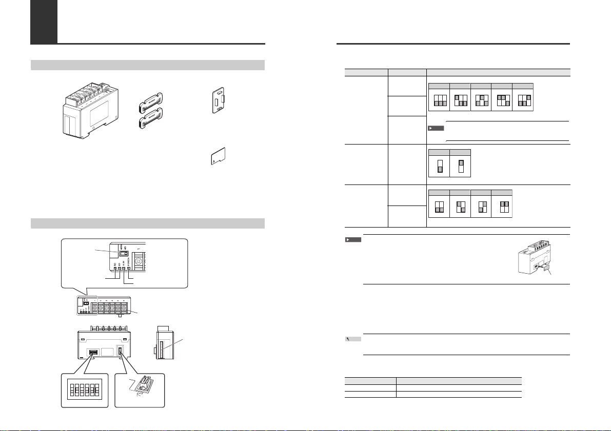
Checking the Package Contents
Before using the DL-RS1A, check that the following items are all included.
All possible care was taken in packaging before shipment. However, in the event of defective broken,
or missing items, please contact your nearest KEYENCE office.
Part Names and Functions
End unit x 2
OP-26751
RS-232C communication unit
DL-RS1A
Expansion connector cover
Switch protection sticker
Instruction manual
102#345
6
G
D
3.
Sensor amplifier connecto
r
(for panel mount type/
large display type)*
10
2N345
6
* A sticker is attached as factory default.
4. Communication
status indicators (green)
5. Alarm indicator (red)
6. Read/write
setting switch
7. Power indicator (green)
8. Communication terminal block
1.
Communication setup switch
2.
Sensor amplifier connector
(for DIN rail mount type)
Before Using the Unit
(1) Communication setup switches
You can use different ON/OFF combinations to configure the communication settings.
• Make sure you cycle the power to the unit after modifying the
communication settings. The modifications are not applied to the
unit until it is powered down and power has been reapplied.
• Place the switch protection sticker supplied with the unit over the
switches after you modify the settings.
(2) Sensor amplifier connector (for DIN-rail mount type)
Use this connector to connect DL-RS1A to a DIN-rail mount type sensor amplifier.
(3) Sensor amplifier connector (for panel mount type)
Use this connector to connect DL-RS1A to a panel mount type sensor amplifier.
The optional extension cable (OP-35361) must be used for connection.
You cannot connect DL-RS1A simultaneously to a DIN-rail mount type sensor amplifier and
a panel mount type sensor amplifier.
(4) Communication status indicators
These indicators show the communication status of DL-RS1A.
Setting Switch No. Combination
Baud rate
1
* Factory default positions are shown.
Do not use combinations other than those shown above for switches
1, 2, and 3.
2
3
Data bit length
4
* Factory default positions are shown.
Parity
5
* Factory default positions are shown.
6
ON ON
ON
ON
ON
123 123 123 123 123
2400bit/s 4800bit/s
9600bit/s*19200bit/s 38400bit/s
Important
ON4ON
4
8 bit* 7 bit
ON56ON56ON56ON
56
None* Even Odd None
Important
Switch protection sticker
Point
Indicator Behavior
SD Lights up in green while data is being transmitted.
RD Lights up in green while data is being received.
2
Page 5
Before Using the Unit
(5) Alarm indicator
This indicator lights up in red.
For information on the actions you should take when an alarm occurs, refer to "Troubleshooting" (page 21).
After turning on the power, the alarm indicator lights for the following amount of time, and
communication cannot be performed during this time.
(6) Read/write setting switch
Use this switch to allow or prohibit writing to the sensor amplifiers. (You can only manipulate this
switch while the unit is active (turned on).)
(7) Power indicator
Lights up in green when the unit has power.
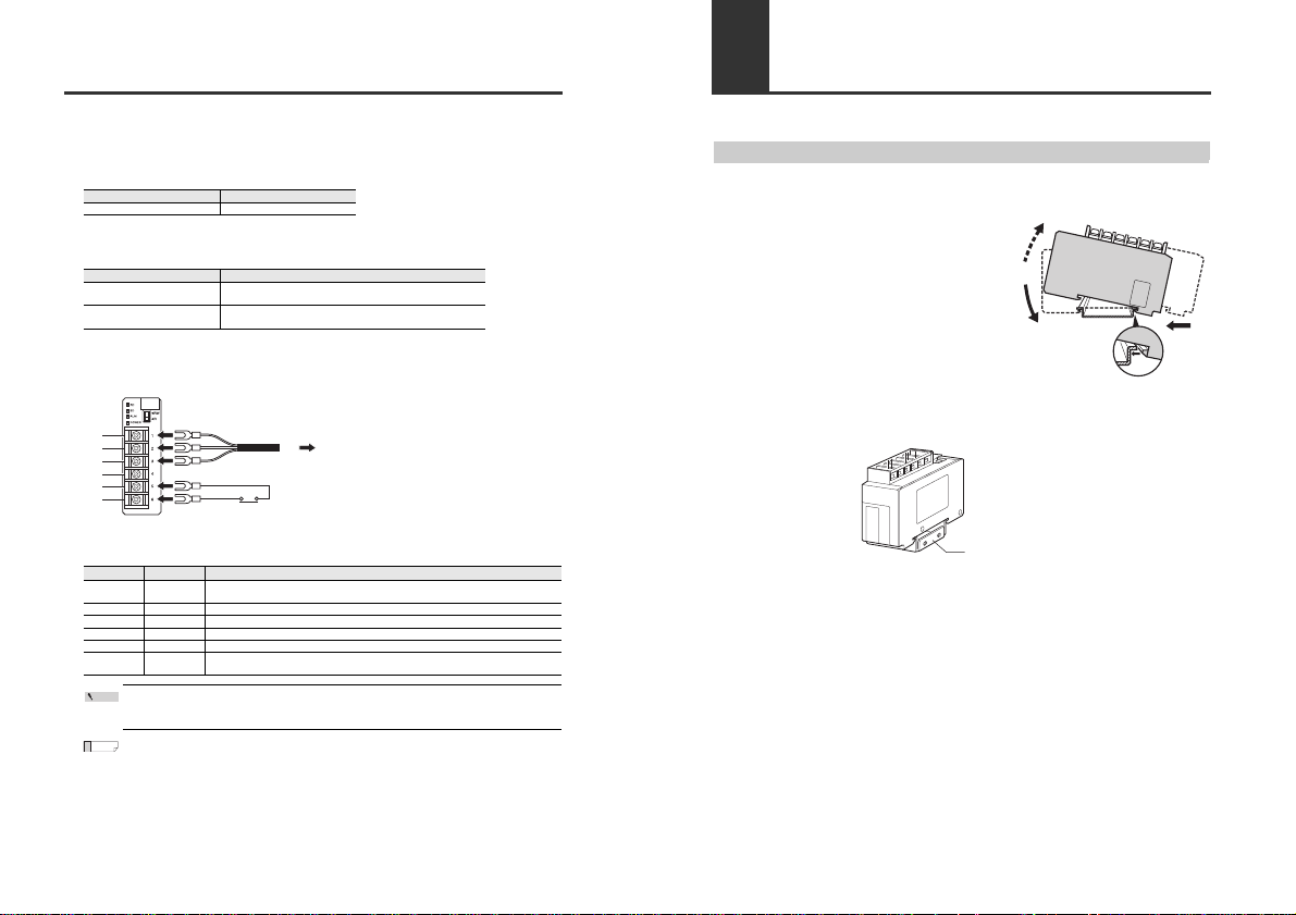
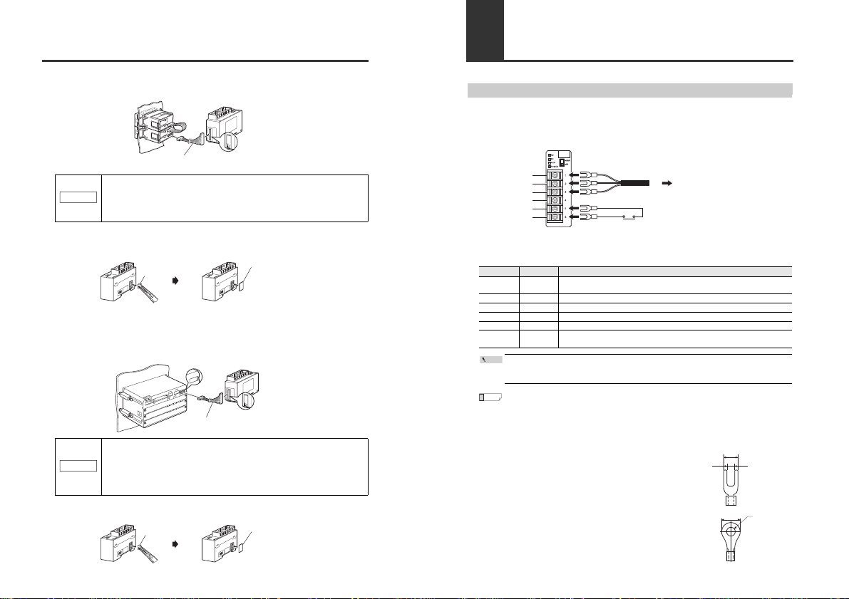
(8) Communication terminal block
Use the terminals on the terminal block to attach communication cables for connecting the unit with external devices.
* Recommended communication cable
KPEV-SP(1P) wire with balanced type twisted shield (strand wire)
Nominal cross-section area 0.16mm
2
(AWG25) min.
A terminal cover is attached to the terminal block.
The terminal cover must be placed over the terminal block when you finish connecting the cables.
The terminals for SG (Nos. 1, 4, and 5) are used in common with the blue wire of the sensor am plifier
main unit.
No. of connected units Incommunicable time
1 to 4 Approx. 2 s
Position of the switch Description
R
(Factory default position)
The unit can read data from the sensor amplifiers. However, it
cannot write settings to the sensor amplifiers.
RW
The unit can both read data from and write settings to the
sensor amplifiers.
SG
RD
SD
SG
SG
DRQ
Communication cable
To external device
KPEV-SP(1P) wire with balanced
type twisted shield (strand wire)
Terminal No.
Terminal Description
1SG
Connects to the shielded wire of the communication cable.
The terminals for SG (Nos. 1, 4, and 5) are internally shor t-circuited.
2 RD (input) Connects to the SD terminal of an external device via a co mmunication cable.
3 SD (output) Connects to the RD terminal of an external device via a communication cable.
4 SG The terminals for SG (Nos. 1, 4, and 5) are internally short-circuited.
5 SG The terminals for SG (Nos. 1, 4, and 5) are internally short-circuited.
6 DRQ (input)
When there is a short-circuit between DRQ and SG, the sensor amplifier data is
transmitted even without a command from the external device.
Point
Reference
Connecting the Unit to Sensor Amplifiers
This section describes how to mount a DL-RS1A and connect it to sensor amplifiers.
Mounting the Unit
■ Mounting the unit on the DIN rail
1 Fit the tab of the lower part of the unit to the
DIN rail. While inserting the unit in the
direction of arrow (1), push the body down in
the direction of arrow (2).
2 To detach the unit, lift the unit in the direction
of arrow (3) while pushing it in the direction
of arrow (1).
When using the mounting bracket (OP-60412), install it as shown in the illustration below.
(1)
(3)
(2)
Mounting bracket:OP-60412
3
Page 6
Connecting the Unit to Sensor Amplifiers
Connecting the Unit to Sensor Amplifiers
You use DL-RS1A by connecting it to sensor amplifiers. The connection method varies according to
the mounting type of the sensor amplifiers.
Before connecting DL-RS1A, you must install the main unit and expansion units of the sensor
amplifiers. For information on installing the sensor amplifiers, refer to the user's manual supplied with
the sensor amplifiers.
Available sensor amplifiers
*1 The IG Series can be used only with the GT-70A Series and the GT2 Series.
When using together with those models, the maximum connectable number is 6. When using
with the IG Series, the maximum number is 4.
To use with 7 or more units, contact your nearest KEYENCE sales office.
Makesurethatthesensoramplifiersareturnedoffbeforeco nnectingtheRS232CcommunicationunitDL-RS1Atothem.Connectingtheunitwhilethesensor
amplifiersareturnedonmaydamagetheunit.
Name Type of amplifier Main unit
Expansion unit
Max. connectable number
Multi-Purpose CCD
Laser Micrometer
IG Series
*1
DIN-rail mount I G-1000 IG-1050
4 units
(Main: 1, Expansion: 3)
Panel mount IG-1500 IG-1550
4 units
(Main: 1, Expansion: 3)
NOTICE
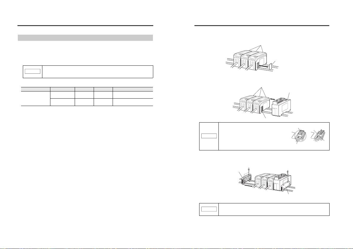
Connecting the Unit to Sensor Amplifiers
Connecting the DL-RS1A to DIN rail mount sensor amplifiers
1
Remove the expansion protective cover from the sensor amplifier that you want to connect to the DL-RS1A.
2
Mount the DL-RS1A on the DIN rail and connect it to the sensor amplifier.
Make sure there is no space between the unit and the sensor amplifier.
3
Mount the end units (OP-26751, two units included) on either side of the sensor amplifier and DL-RS1A u nit and
tighten the two screws on the top of each end unit.
(You can mount the end units in the same way you mount DL-RS1A.)
Sensor amplifier
Expansion protective cover
Sensor amplifier
DL-RS1A
Connector
Checkthatthesensoramplifierconnector(forDIN
railmounting)locatedonthesideofDL-RS1Aisnot
installedatanangleasshownintheillustrationto
theright.Connectingtheunitwithitsconnector
installedatanangletoasensoramplifiermay
damagetheunit.
NOTICE
Sensor amplifier connector
RS-232C communication unit DL-RS1A
End unit
End unit
MakesureyoufirmlyinsertDL-RS1Aallthewayintothesenso ramplifier.Turning
thepoweronwhentheunitisnotinsertedstraightorfirmlyconnectedmay
damagetheunit.
NOTICE
4
Page 7
Connecting the Unit to Sensor Amplifiers
■ Connecting the unit to panel mount sensor amplifiers
1 Connect DL-RS1A to the sensor amplifiers using the optional expansion cable (OP-35361).
2 Remove the sensor amplifier connector with pliers (
for DIN rail mounting when using with panel
mounted sensor amplifiers
) from DL-RS1A unit and install the expansion connector cover
supplied with the unit.
■ Connecting to a large display type sensor amplifier
1 Connect the sensor amplifier to the RS-232C Communication Unit DL-RS1A using the optional
expansion cable (OP-35361).
2 Detach the sensor amplifier connector (DIN rail mount type) of the RS-232C Communication
Unit DL-RS1A with pliers and mount the attached expansion connector.
• Make sure you securely connect the expansion cable while the unit is turned
off. Turning the power on when the cable is not inserted straight or firmly
connected may damage the unit.
• Removing or inserting the cable while the power is on may damage the unit.
• Turn OFF the power before connecting the expansion cable and connect
securely. Diagonal or otherwise improper insertion may damage the
equipment.
• Inserting or pulling the cable when the power is turned ON may damage the
equipment.
Remove the
protection sticke
r
Expansion cable (cable length: 300 mm)
(OP-35361)
NOTICE
Sensor amplifier connector
(for DIN rail mounting type)
Expansion connector cove
r
Detach the
protection sticker
Expansion cable (cable length: 300mm)
Detach the
protection sticker
NOTICE
Sensor amplifier connector
(for DIN rail mount type)
Expansion connector cover
Connecting the Unit to External Devices
Communication Terminal Block
You can connect external devices such as a PC or PLC to the communication terminal block of
DL-RS1A via the communication cables.
■ Terminal connection
* Recommended communication cable
KPEV-SP(1P) wire with balanced type twisted shield (strand wire)
Nominal cross-section area 0.16mm
2
(AWG25) min.
A terminal cover is attached to the terminal block.
The terminal cover must be placed over the terminal block when you finish connecting the cables.
The terminals for SG (Nos. 1, 4, and 5) are used in common with the blue wire of the sensor am plifier
main unit.
● Crimp-type terminal
Use the Y or round terminal for wiring to the I/O terminal.
Use the Y or round terminal with the following dimensions.
Y terminal
Round terminal
SG
RD
SD
SG
SG
DRQ
Communication cable
To external device
KPEV-SP(1P) wire with balanced
type twisted shield (strand wire)
Terminal No.
Terminal Description
1SG
Connects to the shielded wire of the communication cable.
The terminals for SG (Nos. 1, 4, and 5) are internally shor t-circuited.
2 RD (input) Connects to the SD terminal of an external device via a co mmunication cable.
3 SD (output) Connects to the RD terminal of an external device via a communication cable.
4 SG The terminals for SG (Nos. 1, 4, and 5) are internally short-circuited.
5 SG The terminals for SG (Nos. 1, 4, and 5) are internally short-circuited.
6 DRQ (input)
When there is a short-circuit between DRQ and SG, the sensor amplifier data is
transmitted even without a command from the external device.
Point
Reference
Excerpted from dimensions of the Y terminal areas
B: Outer size of Y area
d: Width of inner Y area
(joint area with screw)
Applicable dimension
B: 6mm max.
d: 3.2mm min.
Excerpted from dimensions of the round terminal areas
B: Outer diameter
d: Inner diameter
(joint area with screw)
Applicable dimension
B: 6mm max.
d: 3.2mm min.
B
B
φd
d
5
Page 8
Connecting the Unit to External Devices
■ Connection wiring
Refer to the connection wiring diagram shown below when connecting DL-RS1A to an external
device such as a PC.
• The length of the communication cable must not exceed 15 m.
•
Connect the shield wire of the communication cable to the SG terminal of the external device.
• Make sure that the shield wire does not touch other signal wires or the other terminals on
the terminal block.
■ Optional cable
An optional cable shown below is used to connect to an external device such as a PC that has
a D-sub 9-pin I/O connector.
Part number: OP-81283
Pin layout for D-sub 9-pin connector
*1 Pin numbers 4 and 6 are connected inside the connector.
*2 Pin numbers 7 and 8 are connected inside the connector.
*3 Two cables (black and black/white) are connected to the pin number 5.
SD
RD
DR
ER
RS
CS
SG
2
1
3
4
5
6
RD
SG
SD
SG
SG
DRQ
DL-RS1A
External device
(D-sub 9-pin)
Shield
Point
Pin No. Cable color
1-
2 Red/white
3Red
4
*1
-
5 Black, black/white
*3
6*1-
7
*2
-
8
*2
-
9-
33.2
25
16
5000
39.5
1
50
φ7.1
Front
5
96
1
Connecting the Unit to External Devices
Sample wiring
*1 Insulate either the black or black/white cable that is not used.
*2 Connect the shield wire to the SG terminal of DL-RS1A. (Shield wire is connected to the
connector casing.)
The green and green/white-striped wires are not connected to any of the connector pins.
■ Input circuit diagram
* The terminals for SG (Nos. 1, 4, and 5) are connected internally with the blue wire of the sensor
amplifier main unit.
2
3
4
5
6
7
RD
Red/White
Red
SD
DR
SG
ER
RS
8CS
2
1
3
4
5
6
RD
SG
SD
SG
SG
DRQ
Black, Black/White
*
1
DL-RS1A
(Communication terminal block)
External device
(D-sub 9-pin)
Shield
*2
Reference
Main circuit
(Short-circuit current: 1 mA max.)
6 (DRQ)
+5V
1,4,5 (SG)
*
6
Page 9
Communication Specifications
This section provides the communication specifications of DL-RS1A and describes how to configure the unit.
Communication Specifications
The following table lists the communication specifications for DL-RS1A.
For communication settings, refer to pa ge 2.
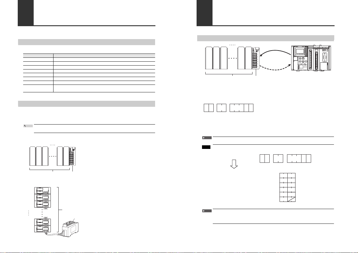
Sensor Amplifier ID Number Assignments
When the main sensor amplifier that is connected to DL-RS1A supports expansion units, the main
sensor amplifier ID number "00" is automatically assigned to the main unit and ID numbers "01 to 14"
to the expansion units.
You cannot change the assignment of sensor amplifier ID numbers.
■ DIN rail mount sensor amplifiers
■ Panel mount sensor amplifiers
Item Specifications
Communication method Full duplex
Synchronization method Asynchronous
Transmission code ASCII
Communication speed 2400, 4800, 9600, 19200, 38400 bit/s (Factory default: 9600 bit/s)
Data bit length 7 or 8 bits (Factory default: 8 bits)
Parity check None, even, odd (Factory default: none)
Stop bit length 1 bit
Data delimiter
Receive: automatically detect CR or CR + LF
Send: fixed to CR + LF
Point
ID No. 00
Main Exp. Exp. Exp. Exp.
01 02 04 05
Sensor amplifier DL-RS1A
ID No. Sensor amplifier
00
01
02
04
05
Main
Exp.
Exp.
Sensor amplifier
Exp.
Exp.
DL-RS1A
Commands and Responses
Overview of Commands and Responses
■ Command format
You can send specific commands based on ASCII codes from an external device to DL-RS1A.
For information on the parameters used in the command, refer to "Parameters of Commands and
Responses" (page 10).
Sample command format structure
(1) With the first two bytes, specify the communication command.
(2) Specify the ID number assigned to the target sensor amplifier using two digits (ASCII characters).
(3) Specify the data number for the data you want to read from or write to the sensor amplifier using
three digits (ASCII characters).
(4) Insert CR or CR + LF as the command delimiter.
You must use commas (,) to separate (1), (2), and (3).
To read the "Hold function setting (data number: 134)" from an expansion unit of an active
IG Series (ID number: 01):
From an external device, 11-byte data will be sent to the DL-RS1A.
The last byte of the command you send must be CR (0DH) or LF (0AH). Specifying a value
other than CR or LF results in an error response (error number: 00). For information on the
error responses, refer to "Error numbers" (page 16).
ID No. 00
Main Exp. Exp. Exp. Exp.
01 02 04 05
Sensor amplifier DL-RS1A
External device like PLC or PC
Response
or
error response
Command or DRQ input
S
(1) (2) (3) (4)
R CR LFID No. Data No.
,,
Important
Example
S
(53H) (52H) (2CH)(31H) (33H) (34H)(0DH)(0AH)(2CH)(30H) (31H)
RCRLF0 1 1 3 4
,,
Command :
S
(53H)
,
(2CH)
R
(52H)
0
(30H)
1
(31H)
1
(31H)
,
(2CH)
3
(33H)
4
(34H)
LF
(0AH)
CR
(0DH)
ASCII character conversion :
Data memory 0
Data memory 1
Data memory 2
Data memory 3
Data memory 4
Data memory 5
→ 5352
H
Value to store in
data memory (hexadecimal)
→ 2C30H
→ 362CH
→ 3130H
→ 310DH
→ 0A00H
bit
15
bit
0
Important
7
Page 10

Commands and Responses
■ Response
When DL-RS1A successfully receives a command from the external device, it automatically returns a
response based on ASCII codes.
For information on the parameters used in the response, refer to "Parameters of Commands and
Responses" (page 10).
Sample response structure
(1) Contains the same communication command as the received command.
(2) Contains the same ID number as the received command.
(3) Contains the same data number as the received command.
(4) Contains the data that DL-RS1A retrieved from the specified sensor amplifier. Contains maximum
of 10 bytes according to the specified data number (3).
(5) Contains CR + LF as the response delimiter.
When the command format "SR,01,134CRLF" is sent to the IG Series (ID number: 01) in
operation and the response indicating that the setting is "Peak hold" is received:
DL-RS1A sends the response to the external device.
S
(1) (2) (3) (4) (5)
R ID No. Data No.
,,
CR LFData
,
Example
S
(53H) (52H) (2CH)(31H) (33H) (34H)(2CH)(3CH) (31H)
R 0 1 1 3 4
,,
(2CH)(31H) (0DH) (0AH)
1 CR LF
,
Response format :
Peak hold
S
(53H)
,
(2CH)
R
(52H)
0
(30H)
1
(31H)
1
(31H)
,
(2CH)
3
(33H)
1
(31H)
LF
(0AH)
CR
(0DH)
ASCII character conversion:
5352
H →
Value to store in
data memory
(hexadecimal)
2C30H →
362C
H →
3130
H →
320D
H →
0A00
H →
bit
15
bit
0
4
(34H)
312CH →
,
(2CH)
Commands and Responses
■ Error response
If DL-RS1A could not receive a command from the external device or if the received command
included an error, it automatically returns an "error response" based on ASCII codes.
For information on the parameters used in the error response, refer to page 10.
Sample error response structure
(1) Contains "ER".
(2) Contains the same communication command as the received command.
(3) Contains a two-digit error number (ASCII characters) indicating the error type.
For information on the error numbers, refer to "Error numbers" (page 16).
(4) Contains CR + LF as the error response delimiter.
An error response indicating an "ID number error" as a response to the command
"SR,01,134CRLF":
DL-RS1A sends the error response to the external device.
E
(1) (2) (3)
R
,,
Error No.
SR
(4)
CR LF
Example
E
(45H) (52H) (2CH)(2CH)(53H) (52H)
R S R
(36H) (35H)
6 5
,,
Error response :
ID No. error
E
(45H)
,
(2CH)
R
(52H)
S
(53H)
R
(52H)
6
(36H)
,
(2CH)
5
(35H)
CR
(0DH)LF(0AH)
ASCII character conversion :
4552
H →
Value to store
in data memory
2C53H →
522C
H →
3635
H →
0D0A
H →
bit
15
bit
0
(0DH) (0AH)
CR LF
8
Page 11

Commands and Responses
Reading
External devices such as PLC's use the following communication commands to read data from
DL-RS1A.
Read from the specified sensor amplifier (SR command)
Command
Response
Error response
* The data length is different depending on the data being read. (Up to 10 characters)
Read all data from all sensor amplifiers (M0 command)
Command
Response
Error response
SR CR LFID No. Data No.
,,
SR Data*ID No. Data No.
,, ,
CR LF
ER,SR
Error No.,CR LF
M 0 CR LF
M0 CR LF
Data of the sensor
amplifier with ID:00
,
Data of the sensor
amplifier with ID:01
……
,
Data of the sensor amplifier
with the last ID No.
,,
ER CR LF
,M0,
Error No.
Commands and Responses
Read output states and data from all sensor amplifiers (MS command)
Command
Response
Error response
Read with external input to the DRQ terminal (DRQ read)
You can send an input signal (by short-circuiting DRQ (terminal number 6) and SG (terminal number
1, 4, or 5)) from an external device such as a PLC instead of sending a command.
Response
Error response
M S CR LF
M
S
Control
output
Control
output
Control
output
CR LF
Data of the sensor
amplifier with ID:00
,, ,,
Data of the sensor
amplifier with ID:01
…
Data of the sensor
amplifier with the last ID No.
,,
Sensor amplifier with ID:00 Sensor amplifier with ID:01 Sensor amplifier with the last ID No.
ER CR LF
,MS,
Error No.
2 ms min.
Input signal
ON
OFF
SG
RD
SD
SG
SG
DRQ
DR
Control
output
Control
output
Control
output
CR LF
Data of the sensor
amplifier with ID:00
,, ,,
Data of the sensor
amplifier with ID:01
…
Data of the sensor
amplifier with the last ID No.
,,
Sensor amplifier with ID:00 Sensor amplifier with ID:01 Sensor amplifier with the last ID No.
ER CR LF
,DR,
Error No.
9
Page 12

Commands and Responses
Writing
External devices such as PLC's use the following communication commands to write data to
DL-RS1A.
Attempting to write data with "read-only" attribute results in a communication error and an
error response (error number: 22).
■ Write to the specified sensor amplifier (SW command)
Command
Response
Error response
* The data length is different depending on the data being written.
■ Write to all sensor amplifiers (AW command)
Command
Response
Error response
* The data length is different depending on the data being written.
Point
SW CR LFID No. Data No.
,,
Setting data*
,
SW CR LFID No. Data No.
,,
ER CR LF
,SW,
Error No.
AW CR LFData No.
,
Setting data*
,
AW CR LFData No.
,
ER CR LF
,AW,
Error No.
Parameters of Commands and Responses
This section describes the parameters used with various commands and responses.
■ Communication commands
There are two types of communication commands: read commands and write commands.
• For information on the data, refer to the instruction manual or user's manual supplied with
the sensor amplifiers.
• If commands are sent during the period of approx. 3 seconds after the power is turned on,
the communication error (error number: 22) will occur.
■ ID numbers
This parameter is used with communication commands "SR" and "SW". Specify the ID number of the
target sensor amplifier using two digits (ASCII characters).
(Example) Sensor amplifier with the ID number 00 = 00, sensor amplifier with the ID number 03 = 03
Communication
command
Attribute Description
SR
Read
Reads the data for the specified data number from the sensor amplifier with the
specified ID number.
M0
Reads the comparator value (P.V. value) that DL-RS1A periodically retrieves
from all sensor amplifiers.
MS
Reads the ON/OFF state of the judgment output and edge check output, and
the comparator value (P.V. value) that DL-RS1A periodically retrieves from all
sensor amplifiers.
DRQ input
Reads the ON/OFF state of the judgment output and edge check output, and
the comparator value (P.V. value) that DL-RS1A periodically retrieves from all
sensor amplifiers when a DRQ input is received.
SW
Write
Writes setting data for the specified data number onto the sensor amplifier with
the specified ID number.
AW Writes setting data for the specified data number onto all sensor amplifiers.
Point
10
Page 13

Parameters of Commands and Responses
■ Data numbers
Specify the data number using three digits (ASCII characters).
● Read-only data
The following table lists the types of data that can be read from the IG Series sensor amplifiers.
• Writing read-only data results in a communication error (error number: 22).
• Reading data that cannot be set on the expansion unit results in a communication error
(error number: 22).
• When the 2 heads mode is used for the calculation function, some portion of data format
or reading range of the main unit will be changed.
Data No. Data name Data format
*1
No. of
bytes
Attribute
*2
Data range
033 Sensor amplifier error state*
3
***** 5 R 0 to 65535
036 Judgment output/Edge check output*
4
** 2 R 0 to 15
037 P.V. value*
5 *6
±**.*** 7 R -99.999 to +99.999
038 R.V. value*
5
039 Peak hold value during hold period*5 *
6
040
Bottom hold value during hold period*5 *
6
041 Calculation Value (CALC value)*5 *
6
042 Analog output value ±*.*** or +**.** 6 R
Analog voltage output: -5.000 to +5.000*
7
Analog current output: +04.00 to +20.00*
7
045 T connector connection sensor head * 1 R
1:IG-028 Transmitter
2:IG-010 Transmitter
9:Detection impossible (including
non-connection)
046 R connector connection sensor head * 1 R
1:IG-028 Receiver
2:IG-010 Receiver
9:Detection impossible (including
non-connection)
047 Number of edges ** 2 R 0 to 99*
8
048 Optical axis alignment state * 1 R
0:Optical axis align ment NG (Optical
axis alignment indicator OFF)
1:
Optical axis alignment OK (Optical
axis alignment indicato r ON)
050 Abnormal setting*
9
*1R
0: Normal setting
1: Abnormal setting
051
Zero shift/Zero shift reset execution
result*
10
*1R
0: Executing
1: Normal termination
2: Execution impossible
052
Standard waveform registration request
result
*1R
0:Executing request
1:Normal termination
2:
Standard waveform registration error
1 (light-receiving amount insufficient)
3:Standard wavefor m registration
error 2 (ambient light)
4:Standard wavefor m registration
error 3 (Combination error)
5:Receiver EEPROM error
6:Standard wavefor m registration
error 4 (Abnormal waveform)
7:Errors other than the above
053 Reset request result * 1 R
0: Executing
1: Normal termination
2: Execution impossible
Point
Parameters of Commands and Responses
*1 In the Data format column, "±" indicates that the value can be either "+" or "-" and "*" signifies a
number from "0 to 9".
*2 R: Indicates that the data type can only be read from the sensor amplifiers.
054 EEPROM writing result*
11
*1R
0: Writing
1: Normal termination
2: Writing failure
055
Tolerance tuning/Two-point tuning
execution result
*1R
0: Executing request
1: Normal termination
2: Execution impossible
056 Calibration execution result*
12
*1R
0:Executing
1:Normal termination
2:Span value abnormal termination
3:Offset value abnormal termination
4:Span value/O ffset value abnormal
termination
121 System parameter current state*
13
** 2 R 0 to 15
161
P.V. of pin diameter 1 or pin interval 1*14±**.*** 7 R -99.999 to +99.999
162
P.V. of pin diameter 2 or pin interval 2*14±**.*** 7 R -99.999 to +99.999
163
P.V. of pin diameter 3 or pin interval 3*14±**.*** 7 R -99.999 to +99.999
164
P.V. of pin diameter 4 or pin interval 4*14±**.*** 7 R -99.999 to +99.999
165
P.V. of pin diameter 5 or pin interval 5*14±**.*** 7 R -99.999 to +99.999
166
P.V. of pin diameter 6 or pin interval 6*14±**.*** 7 R -99.999 to +99.999
167
P.V. of pin diameter 7 or pin interval 7*14±**.*** 7 R -99.999 to +99.999
168
P.V. of pin diameter 8 or pin interval 8*14±**.*** 7 R -99.999 to +99.999
169
P.V. of pin diameter 9 or pin interval 9*14±**.*** 7 R -99.999 to +99.999
170
P.V. of pin diameter 10 or pin interval 10*14±**.*** 7 R -99.999 to +99.999
171
P.V. of pin diameter 11 or pin interval 11*14±**.*** 7 R -99.999 to +99.999
172
P.V. of pin diameter 12 or pin interval 12*14±**.*** 7 R -99.999 to +99.999
173
P.V. of pin diameter 13 or pin interval 13*14±**.*** 7 R -99.999 to +99.999
174 P.V. of pin diameter 14*
14
±**.*** 7 R -99.999 to +99.999
175
R.V. of pin diameter 1 or pin interval 1*14±**.*** 7 R -99.999 to +99.999
176
R.V. of pin diameter 2 or pin interval 2*14±**.*** 7 R -99.999 to +99.999
177
R.V. of pin diameter 3 or pin interval 3*14±**.*** 7 R -99.999 to +99.999
178
R.V. of pin diameter 4 or pin interval 4*14±**.*** 7 R -99.999 to +99.999
179
R.V. of pin diameter 5 or pin interval 5*14±**.*** 7 R -99.999 to +99.999
180
R.V. of pin diameter 6 or pin interval 6*14±**.*** 7 R -99.999 to +99.999
181
R.V. of pin diameter 7 or pin interval 7*14±**.*** 7 R -99.999 to +99.999
182
R.V. of pin diameter 8 or pin interval 8*14±**.*** 7 R -99.999 to +99.999
183
R.V. of pin diameter 9 or pin interval 9*14±**.*** 7 R -99.999 to +99.999
184
R.V. of pin diameter 10 or pin interval 10*14±**.*** 7 R -99.999 to +99.999
185
R.V. of pin diameter 11 or pin interval 11*14±**.*** 7 R -99.999 to +99.999
186
R.V. of pin diameter 12 or pin interval 12*14±**.*** 7 R -99.999 to +99.999
187
R.V. of pin diameter 13 or pin interval 13*14±**.*** 7 R -99.999 to +99.999
188 R.V. of pin diameter 14*
14
±**.*** 7 R -99.999 to +99.999
Data No. Data name Data format
*1
No. of
bytes
Attribute
*2
Data range
11
Page 14

Parameters of Commands and Responses
*3 You can read data number "033" to check the error status of the sensor amplifiers.
Convert the five digit number (ASCII characters) read from the sensor amplifiers to a binary
number and check the ON/OFF state of each bit to check the error.
For information on each error, refer to "IG Series User's Manual".
•
When the data read from a sensor amplifier is "00033":
"33" converted to binary number is "0000 0000 0010 0001".
Therefore, this data indicates that a "receiver error" and an "overcurrent error" have
occurred at the sensor amplifier from which it was read.
•
If no error has occurred at the sensor amplifier, the data "00000" is returned.
*4 You can read data number "036" to check the judgment output status.
Convert the two digit number (ASCII characters) read from the sensor amplifiers to a binary
number and check the ON/OFF state of each bit to check the judgment output status.
•
When the data read from a sensor amplifier is "12":
"12" converted to binary number is "1100".
Bit Sensor amplifier errors
0 Overcurrent error
1 EEPROM error
2 Head error
3 Transmitter/Receiver reverse connection error
4 Receiver EEPROM error
5 Receiver error
6 Transmitter error
7 Transmitter laser error
8 Model mismatch error
9 Head error (Register the standard waveform)
10 Standard waveform registration e rror 1, 2, 3, 4
11 Communic ation error
12 Additional se tting error
13 Calculati on error
Bit Judgment output
0 0: HIGH judgment output OFF, 1: HIGH judgment output ON
1 0: LOW judgment output OFF, 1: LOW judgment output ON
2 0: GO judgment output OFF, 1: GO judgment output ON
3 0: Edge check output OFF, 1: Edge check output ON
Reference
Bit 5: receiver error Bit 0: Overcurrent error
Reference
Bit 3: Edge check output ON Bit 0: HIGH judgment output OFF
Bit 2: GO judgment output ON Bit 1: LOW judgment output OFF
Parameters of Commands and Responses
*5 When the data read from the sensor amplifiers is one of the following values, it is not a
comparator value but has a specific meaning.
*6 When reading data from the main unit on which the 2 heads mode is set for the calculation
function, the reading range is changed to -999.99 to +999.99
*7 When the sensor amplifier is in the error state, the analog voltage output is +5.500 and analog
current output is +03.00.
*8 If the number of edges is 100 or more, 99 is read.
*9 When writing is performed to set the prohibited combination of functions, the value becomes 1.
For details of each function, refer to the User's Manual.
(Example) When the measurement mode is set to "Pin interval judgment mode" or "Pin diameter
judgment mode", and the setting is changed to use the calculation function,
*10 The execution result for the item last requested, either the zero shift execution request or zero
shift reset execution request, is read.
*11 This item includes the results for the initial reset execution or system parameter set request.
*12 When the measurement mode is set to the "Pin interval judgment mode" or "Pin diameter
judgment mode", if the calibration is performed, the value becomes 4 (Abnormal termination of
Span value/Offset value).
*13 You can read data number "121" to check the system parameter of the sensor amplifier. The
system parameter means the polarity of judgment output and edge check output, and the
setting for analog output. Convert the two digit number (ASCII characters) read from the sensor
amplifiers to a binary number and check the ON/OFF state of each bit to check the system
parameter.
•
When the data read from a sensor amplifier is "006":
"6" converted to binary number is "0110".
Therefore, the setting of the amplifier from which the data is read is "NPN output" and
"Analog output 1 to 5 V".
*14 When the measurement mode is set to "Pin interval judgment mode", the pin interval is read.
When it is set to "Pin diameter judgment mode", the pin diameter is read.
The pin diameter (interval) 1 means the first pin diameter (interval) counting from the top side.
When the measurement mode is set to modes other than "Pin interval judgment mode" or "Pin
diameter judgment mode", if this data is read, a communication error (error number: 22) occurs.
Read data Description
+EE.EEE The sensor amplifiers is in the error status.
+99.999 The value exceeds the upper limit of the display range.
-99.999 The value is -99.998 or below the lower limit of the display range.
-99.998 The value is "-----".
Bit Default settings
0 0: NPN output, 1: PNP output
3, 2, 1
000: Analog output OFF
001: 0 to 5 V
010: -5 to 5 V
011: 1 to 5 V
100: 4 to 20 mA
Reference
Bit 3, 2, 1: 1 to 5 V Bit 0: NPN output
12
Page 15

Parameters of Commands and Responses
● Read/write data
The following table lists the types of data that can be read from and written to IG Series sensor
amplifiers.
• Reading or writing data that cannot be set on the expansion unit results in a
communication error (error number: 22).
• When using the 2 heads mode for the calculation function, if the data number 057 (Timing
input request) is read from or writing to the expansion unit additionally installed next to the
main unit, a communication error (error number: 22) occurs.
Data
No.
Data name
Data
format*
1
No. of
bytes
Attribute*
2
Data range Default value
001 Zero shift execution request * 1
R 0 - 1: Last written value
1
W0 o 1: Perform zero shift*
3
002 Zero shift reset execution request * 1
R 0 - 1: Last written value
1
W0 o 1: Perform zero shift reset*
3
003
Standard waveform registration
request
*1
R 0 - 1: Last written value
1
W0 o 1:
Perform standard waveform registration*
3
004 Reset request * 1
R 0 - 1: Last written value
1
W0 o 1: Perform reset*
3
005 Initial reset request * 1
R 0 - 1: Last written value
1
W0 o 1: Perform initial reset*
3
006
System parameter set request
(When the initial reset is
requested, the system parameter
is changed to the value specified
at the data number 120.)*
4
*1
R 0 - 1: Last written value
1
W0 o 1: Perform system paramete r set*
3
007 Tolerance tuning request * 1
R 0 - 1: Last written value
1
W0 o 1: Perform Tolerance tuning*
3
008
Two-point tuning HIGH side 1st
point confirmation operation request
*1
R 0 - 1: Last written value
1
W0 o 1:
Perform 1st point confirmation operation*
3
009
Two-point tuning HIGH side 2nd
point confirmation operation request
(Determine HIGH setting value.)
*1
R 0 - 1: Last written value
1
W0 o 1:
Perform 2nd point confirmation operation*
3
010
Two-point tuning LOW side 1st
point confirmation operation request
*1
R 0 - 1: Last written value
1
W0 o 1:
Perform 1st point confirmation operation*
3
011
Two-point tuning LOW side 2nd
point confirmation operation request
(Determine LOW setting value.)
*1
R 0 - 1: Last written value
1
W0 o 1:
Perform 2nd point confirmation operation*
3
012
Calibration SET 1 Confirmation
operation request
*1
R 0 - 1: Last written value
1
W0 o 1:
Perform SET1 confir mation operation*
3
013
Calibration SET 2 Confirmation
operation request (Perform calibration.)
*1
R 0 - 1: Last written value
1
W0 o 1:
Perform SET2 confir mation operation*
3
057 Timing input request*
5
*1R/W
0: Timing input OFF
1: Timing input ON
0
058
Laser emission stop input
request*
5
*1R/W
0:
Laser emission stop input OFF (Laser emission)
1:
Laser emission stop input ON (Laser emission stop)
0
059 Bank function*
6
*1
R 0 - 3: Currently operating bank
0
W
0: Switch to bank 0
1: Switch to bank 1
2: Switch to bank 2
3: Switch to bank 3
060 Keylock function * 1 R/W
0: Not key locked state
1: Key locked state
0
065 HIGH setting value (BANK 0)*
7
±**.*** 7 R/W -99.999 to +99.999 +08.000
066 LOW setting value (BANK 0)*
7
±**.*** 7 R/W -99.999 to +99.999 +02.000
067 Shift target value (BANK 0)*
7
±**.*** 7 R/W -99.999 to +99.999 +00.000
Point
Parameters of Commands and Responses
068 Sensitivity setting (BANK 0) * 1 R/W
0: Low sensitivity mode
1: Standard mode
2: High sensitivity mode
3: User
1
069 User Binarize level (Bank 0) ** 2 R/W 10 to 90 25
070 User Filter value (Bank 0) ** 2 R/W 3 to 50 09
071
Specified edges interval measurement
mode: Edge number 1 (BANK 0)
±*** 4 R/W -100 to +100*
8
+001
072
Specified edges interval measurement
mode: Edge number 2 (BANK 0)
±*** 4 R/W -100 to +100*
8
+002
073
Pin interval judgment mode or
Pin diameter judgment mode:
Number of the pins (BANK 0)
** 2 R/W 1-14 02
074 HIGH setting value (BANK 1)*
7
±**.*** 7 R/W -99.999 to +99.999 +08.000
075 LOW setting value (BANK 1)*
7
±**.*** 7 R/W -99.999 to +99.999 +02.000
076 Shift target value (BANK 1)*
7
±**.*** 7 R/W -99.999 to +99.999 +00.000
077 Sensitivity setting (BANK 1) * 1 R/W
0: Low sensitivity mode
1: Standard mode
2: High sensitivity mode
3: User
1
078 User Binarize level (Bank 1) ** 2 R/W 10 to 90 25
079 User Filter value (Bank 1) ** 2 R/W 03 to 50 09
080
Specified edges interval measurement
mode: Edge number 1 (BANK 1)
±*** 4 R/W -100 to +100*
8
+001
081
Specified edges interval measurement
mode: Edge number 2 (BANK 1)
±*** 4 R/W -100 to +100*
8
+002
082
Pin interval judgment mode or
Pin diameter judgment mode:
Number of the pins (BANK 1)
** 2 R/W 1-14 02
097 HIGH setting value (BANK 2)*
7
±**.*** 7 R/W -99.999 to +99.999 +08.000
098 LOW setting value (BANK 2)*
7
±**.*** 7 R/W -99.999 to +99.999 +02.000
099 Shift target value (BANK 2)*
7
±**.*** 7 R/W -99.999 to +99.999 +00.000
100 Sensitivity setting (BANK 2) * 1 R/W
0: Low sensitivity mode
1: Standard mode
2: High sensitivity mode
3: User
1
101 User Binarize level (Bank 2) ** 2 R/W 10 to 90 25
102 User Filter value (Bank 2) ** 2 R/W 03 to 50 09
103
Specified edges interval measurement
mode: Edge number 1 (BANK 2)
±*** 4 R/W -100 to +100*
8
+001
104
Specified edges interval measurement
mode: Edge number 2 (BANK 2)
±*** 4 R/W -100 to +100*
8
+002
105
Pin interval judgment mode or
Pin diameter judgment mode:
Number of the pins (BANK 2)
** 2 R/W 1-14 02
106 HIGH setting value (BANK 3)*
7
±**.*** 7 R/W -99.999 to +99.999 +08.000
107 LOW setting value (BANK 3)*
7
±**.*** 7 R/W -99.999 to +99.999 +02.000
108 Shift target value (BANK 3)*
7
±**.*** 7 R/W -99.999 to +99.999 +00.000
109 Sensitivity setting (BANK 3) * 1 R/W
0: Low sensitivity mode
1: Standard mode
2: High sensitivity mode
3: User
1
110 User Binarize level (Bank 3) ** 2 R/W 10 to 90 25
111 User Filter value (Bank 3) ** 2 R/W 03 to 50 09
112
Specified edges interval measurement
mode: Edge number 1 (BANK 3)
±*** 4 R/W -100 to +100*
8
+001
113
Specified edges interval measurement
mode: Edge number 2 (BANK 3)
±*** 4 R/W -100 to +100*
8
+002
114
Pin interval judgment mode or
Pin diameter judgment mode:
Number of the pins (BANK 3)
** 2 R/W 1-14 02
Data
No.
Data name
Data
format*
1
No. of
bytes
Attribute*
2
Data range Default value
13
Page 16

Parameters of Commands and Responses
115 Sub display's screen * 1 R/W
0: R.V. value screen
1: Analog output screen
2: HIGH setting value screen
3: LOW setting value screen
4: Shift target value setting screen
5: Calculated value display screen
0
116
Tolerance tuning Tolerance
setting width*
9
**.*** 6 R/W 00.000 to 99.999 00.100
117 Calibration function SET1 ±**.*** 7 R/W -99.999 to +99.999 +00.000
118 Calibration function SET2 ±**.*** 7 R/W -99.999 to +99.999 +05.000
119 Calibration Function * 1 R/W
0: Standard
1: User setting
0
120 System parameter*
10
** 2 R/W 0 to 15 00
129 Calculation function*
11
*1R/W
0: The calculation function is not used.
1: Addition mode
2: Subtraction mode
3: 2 Heads mode
0
130 Measurement mode * 1 R/W
0: Edge control/Positioning mode
1: Outer diameter/Width measurement mode
2:
Inner diameter/Opening measurement mode
3: Glass edge mode
4: Pin position measurement mode
5: Pin interval judgment mode
6: Pin diameter judgment mode
7:
Specified edges interval measurement mode
0
131 Measurement direction * 1 R/W
0: Top
1: Bottom
0
132 Averaging*
12
** 2 R/W
0: hsp
1: 1
2: 2
3: 4
4: 8
5: 16
6: 32
7: 64
8: 128
9: 256
10: 512
11: 1024
12: 2048
13: 4096
05
133 Output mode * 1 R/W
0: NO (Normally Open)
1: NC (Normally Close)
0
134 Hold function setting * 1 R/W
0: Sample hold
1: Peak hold
2: Bottom hold
3: Peak-to-peak hold
4: Auto peak hold
5: Auto bottom hold
0
135
Auto peak hold or Auto bottom
hold Trigger level*
7
±**.*** 7 R/W -99.999 to +99.999 +00.100
136 Timing Input * 1 R/W
0: Level
1: Edge
0
137 Delay Timer * 1 R/W
0: Delay timer off
1: On delay timer
2: Off delay timer
3: One shot timer
0
138 Timer value **** 4 R/W 1 to 9999 0060
139 Hysteresis*
9
**.*** 6 R/W 0 to 99.999 00.010
140 Analog Output Scaling * 1 R/W
0: Initial state
1: Free range
0
141 Analog output Lower limi t*
7
±**.*** 7 R/W -99.999 to +99.999 +00.000
142 Analog output Upper limit*
7
±**.*** 7 R/W -99.999 to +99.999 +10.000
143 External input*
13
*1R/W
0: Initial state
1: User setting
0
Data
No.
Data name
Data
format*
1
No. of
bytes
Attribute*
2
Data range Default value
Parameters of Commands and Responses
*1 In the Data format column, "±" indicates that the value can be either "+" or "-" and "*" signifies a
number from "0 to 9".
*2 Indicates that the data can only be read from (R), can only be written to (W), or can be both read
from and written to (R/W) the sensor amplifiers.
*3 The command is executed only when the data is changed from 0 to 1. To re-execute the
command, first change the setting to 0, then change it to 1. Otherwise, the command is not
executed.
If the sensor amplifier is turned OFF after the standard waveform registration is performed, the
previous state before the standard waveform registration is performed is restored. If you wish to
keep the standard waveform registration even after the power is turned OFF, set the saving the
standard waveform function to ON.
If the sensor amplifier is turned OFF after the zero shift is performed, the previous state before
the zero shift is performed is restored. If you wish to keep the zero shift state even after the
power is turned OFF, set the saving zero shift value function to ON.
144 External input 1*
13
*1R/W
0: Zero shift input
1: Bank A input
2: Bank B input
3: Laser emission stop input
4: Not use
0
145 External input 2*
13
*1R/W
0: Reset input
1: Bank A input
2: Bank B input
3: Laser emission stop input
4: Not use
0
146 External input 3*
13
*1R/W
0: Timing input
1: Bank A input
2: Bank B input
3: Laser emission stop input
4: Not use
0
147 External input 4*
13
*1R/W
0: Gain input
1: Bank A input
2: Bank B input
3: Laser emission stop input
4: Not use
4
148
Saving the standard waveform
function
*1R/W
0: OFF
1: ON
0
149 Saving zero shift value function * 1 R/W
0: OFF
1: ON
0
150
Interference prevention
function*
14
*1R/W
0: OFF
1: ON
0
151 Display Digit * 1 R/W
1: 0.001
2: 0.01
3: 0.1
4: 1
2
152 Power save function * 1 R/W
0: OFF
1: Half
3: All
0
153 Position monitor * 1 R/W
0: Initial state
1: OK/NG display
2: Red OFF
3: OFF
0
154 Display color * 1 R/W
0: GO Green
1: GO Red
2: Always Red
0
155
Edge check function Number of edges
** 2 R/W 0-99 01
156 Edge check function * 1 R/W
0: OFF
1: Setting A
2: Setting B
0
Data
No.
Data name
Data
format*
1
No. of
bytes
Attribute*
2
Data range Default value
14
Page 17

Parameters of Commands and Responses
*4 The system parameter means the polarity of judgment output and edge check output, and the
setting for analog output.
*5 Only w hen data 0 is written and the external output is OFF for wiring, it operates as OFF
*6 If the sensor amp lifier is in the key locked state, writing is not possible. Writing results in a
communication error (error number: 22).
*7 When reading data from the main unit on which the 2 heads mode is set for the calculation
function, the reading range is changed to -999.99 to +999.99. When the calculation function is
changed from modes other than the 2 heads mode to the 2 heads mode, these setting values
change ten-fold.
*8 -100 means the "Bottom" setting. +100 means the "Top" setting.
*9 When reading data from the main unit on which the 2 heads mode is set for the calculation
function, the reading range is changed to 000.00 to 099.99.
*10 Specify the system parameter set when data number 06 (Initial reset request) is written. Convert
the two digit number (ASCII characters) to a binary number and check the ON/OFF state of
each bit to specify the system parameter.
•
When the specified data is "06":
"6" converted to binary number is "0110".
Therefore, the setting of the amplifier to which the data is written is "NPN output" and
"Analog output 1 to 5 V".
*11 When the calculation function is changed from 3 (2 heads mode) to modes other than 3, or
changed from modes other than 3 to 3 (2 heads mode), the communication response time T4
becomes max. 1 second for 1 second after the setting is changed. Also, the same result is
yielded when the setting is changed using the button operation of the sensor amplifier. When
the calculation function is changed, T6 becomes max. 100 ms. For T4 and T6, refer to
"Communication Response Time" (page 17).
*12 When the measurement mode is set to the "Pin interval judgment mode" or "Pin diameter
judgment mode", the data 0 and 10 to 13 cannot be written. If 0 is written, data 1 is written. If 10
to 13 is written, data 9 is written.
Do not perform writing to the expansion unit 1 when the calculation function is used. If the
average number of times of the main unit is changed using the calculation function, the average
number of times of the expansion unit 1 is automatically changed.
*13 To reflect the setting written for the data number 144 to 147 to the sensor amplifier, write 1 (user
setting) for the data number 143 or set the external input setting to "User setting" with the button
operation on the sensor amplifier.
*14 Writing is possible only for the main unit with the IG Series expansion unit additionally installed
next to the main unit. Writing onto other sensor amplifiers results in a communication error (error
number: 22).
Bit Default settings
0 0: NPN output, 1: PNP output
3, 2, 1
000: Analog output OFF
001: 0 to 5 V
010: -5 to 5 V
011: 1 to 5 V
100: 4 to 20 mA
Reference
Bit 3, 2, 1: 1 to 5 V Bit 0: NPN output
Parameters of Commands and Responses
● Relation between the data number 001 to 013 (data requesting the sensor amplifier operation)
and the data number 051 to 056 (data presenting the result of request/execution)
When writing the data number 001 to 013 (data requesting the sensor amplifier operation), read the
data number 051 to 056 (data presenting the result of request/execution) and check that the request
is correctly reflected (1: Normal termination is read.). If the request is not correctly reflected and
abnormal termination occurs, data other than 1: Normal termination may be read by reading the data
number 051 to 056. Thus, the request may not be reflected to the sensor amplifier.
When 0 o 1 is written for the data number 001 to 013, the previous state of the data number 051 to
056 is cleared and the condition is updated. The data number 051 to 056 keeps the result until 0 o 1
is written for the data number 001 to 013 next.
(Example) Relation between the data number 003 (Standard waveform registration request) and the
data number 052 (Standard waveform registration request result)
When the target object is present within the measurement range and the optical axis
alignment indicator is off, if the standard waveform registration is performed, the results
are as follows.
(1) When the power is turned on, the default condition for the data number 003 becomes
1: Normal termination.
(2) If 0 is written for the data number 003, the data number 052 keeps 1: Normal
termination.
(3) If 1 is written for the data number 003, the data number 052 is changed to 0: Executing
request.
(4) Although the standard waveform registration was performed, the standard waveform
registration error 1 occurs due to the insufficient light-receiving amount. Then, the data
number 052 is changed to 2: Standard waveform registration error 1.
(5) The data number 052 keeps 2: Standard waveform registration error 1 until the
standard waveform registration is requested again or the power is turned on again.
• The data number 051 (Zero shift/zero shift reset execution result) keeps the result of
writing which either the data number 001 (Zero shift execution request) or data number
002 (Zero shift reset execution request) performed last.
• The data number 055 (Tolerance tuning/Two-point tuning execution result) keeps the result
of writing which any of the data number 007 (Tolerance calibration request), data number
009 (Two-point calibration, HIGH side 2nd point confirmation) or data number 011 (Twopoint calibration, LOW side 2nd point confirmation) performed last.
• The data number 054 (EEPROM writing result) keeps "0: Writing" approx. for 2 seconds
after the contents written onto the nonvolatile memory (EEPROM) using the writing
commands (SW, AW) are sent last. If writing starts after 2 seconds and finishes normally,
1: Normal termination results.
(Example) If the writing commands (SW, AW) are continuously sent every second, 0:
Writing results always. After the last writing commands (SW, AW) are sent, 0:
Writing is kept for 2 seconds, writing is performed after 2 seconds and 1:
Normal termination results.
However, the initial reset is performed for the data number 005 (Initial reset request), writing
starts immediately. If the all parameters can be saved on the nonvolatile memory (EEPROM)
after approx. 3 seconds, 1: Normal termination results.
Point
15
Page 18

Parameters of Commands and Responses
■ Control outputs (Judgment outputs)
This parameter is used with communication command "MS" and DRQ input. For the IG Series, specify
the ON/OFF state of the judgment output (HIGH/LOW/GO judgment output) and edge check output
using two digits (ASCII character).
Convert the two digit number (ASCII characters) read from the sensor amplifiers to a binary number
and check the ON/OFF state of each bit to check the judgment output status.
When the data read from a sensor amplifier is "12":
"12" converted to binary number is "1100".
Bit Judgment output
0 0: HIGH judgment output OFF, 1: HIGH judgment output ON
1 0: LOW judgment output OFF, 1: LOW judgment output ON
2 0: GO judgment output OFF, 1: GO judgment output ON
3 0: Edge check output OFF, 1: Edge check output ON
Reference
Bit 3: Edge check output ON Bit 0: HIGH judgment output OFF
Bit 2: GO judgment output ON Bit 1: LOW judgment output OFF
Parameters of Commands and Responses
■ Error numbers
The following table lists the error numbers that are returned as error responses when errors occur in
the communication with the IG Series.
Each error number is identified with two digits (ASCII characters).
The commands are only sent and received when a response is returned from DL-RS1A to the
external device within 1 sec.
Take the appropriate action to resolve the problem by referring to "Troubleshooting" (page 21).
Error
number
Error name Problem Action
00
Invalid command
error
An invalid command was
received.
Make sure that the external device has
sent a command listed in
"Communication commands" (page 10).
20 Data length error
Data with the correct length was
not received.
Make sure that the external device has sent
either "CR" or "CR + LF" as a data delimiter.
21
Number of
parameters error
The correct number of parameters
for the command was not
received.
Make sure that the number of parameters
and the positions of the commas used as
data delimiters conform to the command
format shown in "Commands and
Responses" (page 7).
22 Parameter error
· A parameter exceeds its range
of value.
· The external device is trying to
write a data type that cannot be
written.
· The external device is trying to
read a data type that cannot be
read.
· The data format is incorrect.
Make sure that the external device is
sending a command listed in
"Communication commands" (page 10).
29 Communication error
An error was detected with
RS-232C communication.
Make sure that DL-RS1A and the external
device have the same communication
settings configured. For information on
configuring DL-RS1A, refer to "(1)
Communication setup switches" (page 2).
65 ID number error
The ID number specified with the
command is incorrect.
Make sure that the sent data specified as
the ID number is a 2-digit number (ASCII
characters) according to the number of
connected units.
66 Expansion line error
The communication could not be
established due to a problem with
an expansion line.
Check that each of the sensor amplifiers
and DL-RS1A are securely and properly
connected by referring to "Connecting
the Unit to Sensor Amplifiers" (page 3).
Make sure that sensor amplifiers that are
supported by DL-RS1A are connected
(refer to page 4).
67 Write control error DL-RS1A is not writable.
Change the read/write setting switch to
the R/W position to enable writing to DLRS1A. For information on the read/write
setting switch, refer to "Part Names and
Functions" (page 2).
Point
16
Page 19

Communication Response Time
This section describes the communication response time for each communication command and
various time frames.
Communication Response Time and Time Chart
This section describes the concept of communication response time and the time chart for the
communication commands.
When sending communication commands consec utively from the external device, wait to send
the next command after reception of the response for the previous command from DL-RS1A
completes.
■ SR command
The SR command directly reads data from a sensor amplifier during T4 (DL-RS1A command
processing time).
Time chart
■ M0 command and MS command
The M0 and MS commands read the buffered data that DL-RS1A periodically retrieves from the
sensor amplifiers.
Therefore, the latest data detected by the sensors can only be read after T2 (DL-RS1A data
processing time) where DL-RS1A retrieves data from the sensor amplifiers.
Point
External device
DL-RS1A
T5
T3
T4
T3: Command format send time from external device
T4: DL-RS1A command processing time
T5: Response send time from DL-RS1A
* For the specific values (times) of T3 to T5, refer to
"Time Frames of Communication Response Time" (page 18).
Sensor amplifier
DL-RS1A
T1
T2
External device
T3
T5
T4
T1: Sensor amplifier response time (Refer to the instruction manual of the sensor amplifier.)
T2: DL-RS1A data processing time
T3: Command format send time from external device
T4: DL-RS1A command processing time
T5: Response send time from DL-RS1A
Detection
* For the specific values (times) of T2 to T5, refer to
"Time Frames of Communication Response Time" (page 18).
Communication Response Time
■ DRQ input
The data read in response to a DRQ input is the buffered data that DL-RS1A periodically retrieves
from the sensor amplifiers.
Therefore, the latest data detected by the sensors can only be read after T2 (DL-RS1A data
processing time) where DL-RS1A retrieves data from the sensor amplifiers.
Time chart
■ SW command and AW command
The SW and AW commands are write commands.
Time chart
Sensor amplifier
DL-RS1A
T1
T2
DRQ input
T5
T4
Detection
↓
2 ms min.
T1: Sensor amplifier response time (Refer to the instruction manual of the sensor amplifier.)
T2: DL-RS1A data processing time
T4: DL-RS1A command processing time
T5: Response send time from DL-RS1A
* For the specific values (times) of T2 to T5, refer to
"Time Frames of Communication Response Time" (page 18).
External device
DL-RS1A
T5
T3
T4
Sensor amplifier
T6
T3: Command format send time from external device
T4: DL-RS1A command processing time
T5: Response send time from DL-RS1A
T6: Sensor amplifier setting change time
* For the specific values (times) of T3 to T6, refer to
"Time Frames of Communication Response Time" (page 18).
17
Page 20

Communication Response Time
• For the IG Series, when the data to which the setting written onto the sensor amplifier
using SW command and AW command is reflected is read using the reading command
(M0, MS) or DRQ input, perform this operation after additional time T elapses after the
response from the DL-RS1A is finished.
Time T varies depending on the data number.
(1) Data number corresponding to T=Response time (When the calculation function is
used: Response time + T2)
If reading is performed before T elapses, the data prior to the setting change is read.
• Data number 132: Averaging
• Sensitivity setting of the BANK currently selected (example: When the current BANK
is BANK 0, data number 068: sensitivity setting (BANK 0))
• If the sensitivity setting of the BANK currently selected is User: Binarize level or Filter
value (example: When the current BANK is BANK 0, data number 069: User Binarize
level (BANK0) and data number 070: User Filter value (BANK 0))
(2) Data number corresponding to T=Response time (When the calculation function is
used: Response time + T2)
If reading is performed before T elapses, -99.998 meaning "-----" is read as a P.V. value.
• Data number 059: Bank function
• Data number 130: Measurement mode
(3) Data number corresponding to T=Response time + 100 ms
If reading is performed before T elapses, -99.998 meaning "-----" is read as a P.V. value.
• Data number 129: Calculation function
(4) Data number corresponding to T=0 (When the calculation function is used: T2)
• Data numbers other than (1) to (3)
Point
Communication Response Time
Time Frames of Communication Response Time
This section describes the communication time frames (T2 to T6).
The maximum time required is shown for each time frame. However, depending on the
actual environment, it may require more time.
■ T2 (DL-RS1A data processing time)
For information on the calculation function, refer to the manual supplied with the sensor amplifiers.
● When calculation function of sensor amplifiers is OFF
*
* This table also applies to the sensor amplifiers that do not have the calculation function.
● When calculation function of sensor amplifiers is ON
■ T3 (Command send time from external device)
Refer to the manual supplied with the external device connected to DL-RS1A.
■ T4 (DL-RS1A command processing time)
The processing time varies according to the command sent from the external device.
● Read commands
● Write commands
Reference
Number of connected
sensor amplifiers
Data processing time (T2)
IG Series
15 ms
210 ms
312 ms
416 ms
Number of connected
sensor amplifiers
Data processing time (T2)
IG Series
15 ms
210 ms
312 ms
416 ms
Communication command
Number of connected
sensor amplifiers
Command processing time (T4)
IG Series
SR
1 11.5 ms
214 ms
315 ms
417 ms
M0/MS/DRQ input
1 to 4
4 ms
Communication command
Number of connected
sensor amplifiers
Command processing time (T4)
IG Series
SW
119 ms
224 ms
328 ms
436 ms
18
Page 21

Communication Response Time
AW
1 56.5 ms
259 ms
360 ms
462 ms
Communication command
Number of connected
sensor amplifiers
Command processing time (T4)
IG Series
Communication Response Time
■ T5 (Response send time from DL-RS1A)
The time required to send a response varies depending on the communication speed, data bit
length, and number of bytes.
For information on the communication settings, refer to page 2.
The response time can be calculated using the following formula:
T5 = (number of bytes) x (data bit length + 4) / (communication speed)
● Number of bytes for different commands
SR command : (number of bytes in the read data) + 12
M0 command : {(number of bytes in the read data) + 1} u number of connected sensor amplifiers + 4
MS command : {(number of bytes in the read data) + 3} u number of connected sensor amplifiers + 4
DRQ input : {(number of bytes in the read data) + 3} u number of connected sensor amplifiers + 4
SW command : 11
AW command : 8
* For information on the number of bytes in the write data and the number of bytes in the read data,
refer to "Parameters of Commands and Responses" (page 10).
Sample calculation
■ T6 (Sensor amplifier settings change time)
For information on the calculation function, refer to the manual supplied with the sensor amplifiers.
● When calculation function of sensor amplifiers is OFF
*
T6 = 0 ms for SW and AW commands; the sensor amplifiers complete modifying their settings during
the T4 period.
* This table also applies to the sensor amplifiers that do not have the calculation function.
● When calculation function of sensor amplifiers is ON
The SW/AW command also becomes T6 = 0 ms.
Number of bytes Data length Communication speed Response time
21 8 bit 9600 bps 26 ms
114 8 bit 9600 bps 143 ms
21 7 bit 38400 bps 6 ms
114 7 bit 38400 bps 33 ms
19
Page 22

Specifications
Performance Specifications
The following table shows the performance specifications for DL-RS1A.
* The number of connectable sensor amplifiers varies depending on the model to be connected.
• IG Series: Up to 4 units (including the main unit)
(When the GT2-70 Series or GT-70A Series is included, the maximum number is 6. When using with the IG Series,
the maximum number is 4. To use with 7 or more units, contact your nearest KEYENCE sales office.)
Communication Specifications
The following table shows the communication specifications for DL-RS1A.
Item Specifications
Model DL-RS1A
Power supply voltage
20 to 30 VDC, including 10% ripple (P-P). Class2
(Supplied from the connected sensor amplifier)
Current consumption 25 mA max.
Number of connectable
sensor amplifiers
Varies depending on the model*
Indicators
2 communication status indicators (green), alarm indicator (red), power indicator
(green)
Environmental
Ambient
temperature
-10 to +55°C (No freezing)
Relative
humidity
35 to 85% RH (No condensation)
Vibration 10 to 55 Hz, compound ampl itude 1.5 mm, 2 hours for each of XYZ axes
Material Main unit housing: polycarbonate
Weight Approx. 53 g
Accessories
Instruction manual, 2 end units, expansion connector cover, switch protection
sticker
Item Specifications
Communication method Full duplex
Synchronization method Asynchronous
Transmission code
ASCII
Communication speed
(Baud rate)
2400, 4800, 9600, 19200, 38400 bit/s
(Factory default: 9600 bit/s)
Data bit length 7 or 8 bits (Factory default: 8 bits)
Parity check None, ev en, odd (Factory default: none)
Stop bit length 1 bit
Data delimiter
Receive: automatically detect CR or CR + LF
Send: fixed to CR + LF
Specifications
Dimensions
■ When the unit is mounted on the DIN rail
■ When the optional fixture (OP-60412) is used
22.5
(48.2)
43.8
37.2
21.1 35.4
70
Unit:mm
2-(4.4x3.4)
37.2
43.8
51.3
31.4
70
15
15
28.5
35.5
22.5
2-φ3.4
5
Unit:mm
20
Page 23

Troubleshooting
Problem Cause Action
The power indicator (POWER)
does not light up.
Power is not
supplied.
Make sure that the voltage of the power supplied to the
sensor amplifier main unit is 20 to 30 VDC.
DL-RS1A is not
properly inserted to
the expansion
connector of the
sensor amplifier.
Reconnect the unit following the instructions in "Connecting
the Unit to Sensor Amplifiers" (page 3).
The alarm indicator lights up
before communication starts.
DL-RS1A is
connected to a
sensor amplifier that
does not support DLRS1A.
Make sure that the unit is connected to an appropriate
sensor amplifier model (refer to "Available sensor amplifiers"
(page 4)).Reconnect the unit following the instructions in
"Connecting the Unit to Sensor Amplifiers" (page 3).
The communication status
indicator (RD) of DL-RS1A does
not flash when you send a
command from an external
device.
The RD terminal of
DL-RS1A is not
connected to the
SD terminal of the
external device.
Check the connection wiring by referring to "Connecting the
Unit to External Devices" (page 5).
No communication
data is sent from the
external device.
Make sure that communication commands are sent out from
the external device.
The alarm indicator lights up
while data is transmitted.
Communication
settings are
incorrect.
Make sure that DL-RS1A and the external device have the
same settings specified for communication speed, data bit
length, and parity check.
For information on configuring DL-RS1A, refer to "Part
Names and Functions" (page 2).
The communication status
indicator (RD) of DL-RS1A
flashes but the communication
status indicator (SD) does not
flash while data is transmitted.
The communication status
indicator (SD) of DL-RS1A
flashes while data is
transmitted, but the data cannot
be retrieved by an external
device.
Proper
communication is
not established.
Lower the communication speed. Use a shielded cable for
the communication cable (refer to "Connecting the Unit to
External Devices" (page 5)). Modify the connection wiring so
that noise does not enter the communication cable.
A communication error
response is returned from DLRS1A while data is transmitted.
For the cause and action, refer to page 16.
ASCII Code Table
The following table lists the ASCII codes.
0
0
1
2
3
4
5
6
7
8
9
A
B
C
D
E
F
123456789
S
P
N
U
L
D
L
E
D
C
1
D
C
2
D
C
3
D
C
4
N
A
K
S
Y
N
E
T
B
C
A
N
S
U
B
E
S
C
S
O
H
S
T
X
E
T
X
E
O
T
E
N
Q
A
C
K
B
E
L
B
S
EMH
T
L
F
V
T
F
F
C
R
S
O
D
E
L
S
I
0 @ P ` p
High-order 4 bits
! 1AQaq
2BRbr
# 3CSc s
$ 4DTd t
% 5EUeu
& 6FV fv
7
Low-order 4 bits
GWg w
( 8HXh x
) 9IYiy
: JZj z
+; K [ k {
,< L\ l|
ー=M ] m }
.> N ^ n
~
/
→
←
↑
↓ ?O_ o
21
Page 24

Page 25

Page 26

Page 27

Revision History
Date of printing Version Revision contents
February 2010
August 2010
Released for each model.First edition
Second edition
WARRANTY
KEYENCE products are strictly factory-inspected. However, in the event of a failure,
contact your nearest KEYENCE office with details of the failure.
1. WARRANTY PERIOD
The warranty period shall be for one year from the date that the product has been delivered
to the location specified by the purchaser.
2. WARRANTY SCOPE
(1) If a failure attributable to KEYENCE occurs within the abovementioned warranty period,
we will repair the product, free of charge. However, the following cases shall be excluded
from the warranty scope.
• Any failure resulting from improper conditions, improper environments, improper handling,
or improper usage other than described in the instruction manual, the user’s manual,
or the specifications specifically arranged between the purchaser and KEYENCE.
• Any failure resulting from factors other than a defect of our product, such as the
purchaser’s equipment or the design of the purchaser’s software.
• Any failure resulting from modifications or repairs carried out by any person other than
KEYENCE staff.
• Any failure that can certainly be prevented when the expendable part(s) is maintained
or replaced correctly as described in the instruction manual, the user’s manual, etc.
• Any failure caused by a factor that cannot be foreseen at a scientific/technical level at
the time when the product has been shipped from KEYENCE.
• Any disaster such as fire, earthquake, and flood, or any other external factor, such as
abnormal voltage, for which we are not liable.
(2) The warranty scope is limited to the extent set forth in item (1), and KEYENCE assumes no
liability for any purchaser’s secondary damage (damage of equipment, loss of opportunities,
loss of profits, etc.) or any other damage resulting from a failure of our product.
3. PRODUCT APPLICABILITY
KEYENCE products are designed and manufactured as general-purpose products for general
industries. Therefore, our products are not intended for the applications below and are not
applicable to them. If, however, the purchaser consults with us in advance regarding the
employment of our product, understands the specifications, ratings, and performance of the
product on their own responsibility, and takes necessary safety measures, the product may
be applied. In this case, the warranty scope shall be the same as above.
• Facilities where the product may greatly affect human life or property, such as nuclear
power plants, aviation, railroads, ships, motor vehicles, or medical equipment
• Public utilities such as electricity, gas, or water services
• Usage outdoors, under similar conditions or in similar environments
Page 28

Copyright (c) 2010 KEYENCE CORPORATION. All rights reserved.
189033E 1080-2 96080E Printed in Japan
 Loading...