


 Loading...
HF / 50MHz ALL MODE TRANSCEIVER
TS-480HX/480SAT
SERVICE MANUAL
© 2003-11 PRINTED IN JAPAN B51-8667-00 (N) 694
|
|
|
Microphone |
|
Cabinet (Upper) |
||||
|
|
|
(T91-0638-05) |
|
(A01-2189-02) |
||||
Panel assy |
|
Knob |
|
Panel |
|||||
(A62-1076-03) |
|
(K29-9265-03) |
|
(A62-1079-01) |
|||||
|
|
|
|
|
|
|
|
|
|
|
|
|
|
|
|
|
|
|
|
|
|
|
|
|
|
|
|
|
|
|
|
|
|
|
|
|
|
|
|
|
|
|
|
|
|
|
|
|
|
|
|
|
|
|
|
|
|
|
|
|
|
|
|
|
|
|
|
|
|
|
|
|
|
|
|
|
|
|
|
|
|
|
|
|
|
|
|
|
|
|
|
|
|
|
|
|
|
|
|
Knob |
Key top |
|
Knob ring |
|
Knob |
|
Foot |
|
(K29-9267-03) |
(K29-9263-02) |
(K29-9264-04) |
(K29-9270-03) |
(J02-0441-05) x 4 |
||||
Knob |
|
Stand |
|
Knob (Main dial) |
Knob |
|
Cabinet (Lower) |
|
(K29-9266-03) |
(J09-0409-03) |
(K21-1105-03) |
(K29-9267-03) |
(A01-2190-02) |
||||
CONTENTS
DISASSEMBLY FOR REPAIR .................................. |
2 |
CIRCUIT DESCRIPTION ........................................... |
3 |
COMPONENTS DESCRIPTION ............................. |
14 |
SEMICONDUCTOR DATA ..................................... |
20 |
PARTS LIST ............................................................ |
27 |
EXPLODED VIEW................................................... |
50 |
PACKING ................................................................ |
54 |
ADJUSTMENT ....................................................... |
55 |
INTERCONNECTION DIAGRAM ........................... |
76 |
PC BOARD / SCHEMATIC DIAGRAM |
|
RF UNIT (X44-327X-XX) .................................... |
78 |
FINAL UNIT (X45-365X-XX) (A/3)..................... |
86 |
FINAL UNIT (X45-365X-XX) (B/3) ..................... |
93 |
FINAL UNIT (X45-365X-XX) (C/3) ..................... |
96 |
FINAL UNIT (X45-366X-XX) (A/3)..................... |
98 |
FINAL UNIT (X45-366X-XX) (B/3) ................... |
105 |
FINAL UNIT (X45-366X-XX) (C/3) ................... |
108 |
DISPLAY UNIT (X54-3410-00) (A/3, B/3, C/3) ....... |
110 |
TX-RX UNIT (X57-663X-XX) (A/2, B/2) .......... |
116 |
SUB UNIT (X58-4900-XX)................................ |
128 |
TERMINAL FUNCTION ........................................ |
129 |
BLOCK DIAGRAM ................................................ |
134 |
LEVEL DIAGRAM ................................................. |
136 |
ACCESSORIES ..................................................... |
140 |
SPECIFICATIONS ................................................. |
141 |

TS-480HX/480SAT
DISASSEMBLY FOR REPAIR
How to remove the torque changeover lever (G02-0898-04)
1.Turn the lever section of the torque changeover lever to the right. ( q )
2.Insert the tip of a flat-head screwdriver into the recessed part of the torque changeover lever. ( w )
3.Lift the torque changeover lever using the tip of the flathead screwdriver. ( e )
Caution: Be careful not to damage the torque changeover lever when lifting it.
4.Turn the lever section of the torque changeover lever to the right, as in the position described in step 3. ( r )
5.Lift the torque changeover lever and remove it from the panel ASSY.
 e
e

 w
w
q
r
How to mount the torque changeover lever (G02-0898-04)
1.Insert the torque changeover lever into the mounting location so that the three tabs align with the torque changeover slots. (Fig.1)
2.Turn the lever section of the torque changeover lever to the left while pressing the surface of the lever as shown in the Fig. 2, and mount it onto the panel ASSY.
Cautions for mounting the main dial knob (K21-1105-03)
Confirm that the lever section of the torque changeover lever is in the fully turned left position (Torque OFF) before mounting the main dial knob.
Cautions for replacing the torque changeover lever
Apply the dry-surf 2400 onto the front and rear surfaces after replacing the torque changeover lever. (Do not apply the dry surf to the lever section.)
Apply the dry-surf 2400 onto the front and rear surfaces of the torque changeover lever.
|
|
|
|
|
|
|
|
|
|
|
|
|
|
|
|
|
|
|
|
|
|
|
|
2 |
Fig. 1 |
Fig. 2 |
|
||||
|
|
|
|
|
|
|
|
TS-480HX/480SAT
CIRCUIT DESCRIPTION
Frequency Configuration
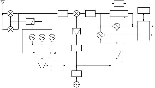
Figure. 1 shows the frequency configuration of this transceiver. All modes operate in a double conversion while transmitting. FM mode operates in a triple conversion and other modes operate in a double conversion while receiving.
ANT |
455kHz |
|
|
|
|
|
TX/RX |
|
|
3rd IF |
|
|
|
|
|
|
|
|
|
|
|
RX MIX |
|
|
73.095MHz |
MIX |
10.695MHz |
|
DSP |
||
|
|
|
1st IF |
|
2nd IF |
FM |
FM IC |
||
|
|
|
|
|
|||||
|
73.125~ |
|
|
|
|||||
|
|
|
|
|
|
|
|
||
LO1 |
133.095MHz |
|
|
|
|
Except RX MIX |
|
||
|
|
|
|
|
|
|
|
||
|
|
|
|
|
LO2 |
|
FM |
|
AF OUT |
|
|
|
|
|
|
|
|
||
|
|
|
|
|
|
|
|
|
|
VCO1 |
VCO2 |
VCO3 |
|
|
|
TX |
|
CAR |
CODEC |
TX MIX |
|
|
|
|
|
|
|
MIC IN |
|
|
|
|
|
|
|
MIX |
|
|
|
|
|
|
|
|
|
|
|
|
|
|
|
|
|
|
62.4MHz |
CAR |
|
|
|
|
|
|
|
|
|
|
|
||
|
|
|
|
|
x2 |
|
|
10.695MHz (Except FM) |
|
|
|
|
|
|
|
|
10.24MHz (FM) |
|
|
|
PLL |
|
|
|
|
|
|
||
|
FM MOD |
|
|
|
|
|
|||
|
LMX2360 |
|
|
|
|
|
|||
|
|
|
|
|
|
|
|
||
|
|
PLL REF |
|
|
|
|
|
|
|
8.33~ |
|
|
DDS |
DDS REF |
|
DDS REF |
DDS |
|
|
8.47MHz |
AD9835 |
|
31.2MHz |
|
AD9835 |
|
|||
|
CF1 |
|
|
|
|
|
|||
|
|
|
x2 |
|
|
|
|
||
|
|
|
|
|
|
|
|
|
|
fstd
X1
15.6MHz
Fig. 1 Frequency configuration
Reference Signal Generator
The reference frequency (fstd), which is used to control the PLL frequency, oscillates at 15.6MHz in a crystal oscillation circuit (X1, Q1). This 15.6MHz signal passes through a buffer amplifier (Q4) and is doubled in a multiplier (Q5) to generate a 31.2 MHz signal. The 31.2MHz signal is used as the reference signal for the DDS (IC1) for the PLL reference signal of the first local oscillator (LO1) and the DDS (IC2) for a carrier (CAR).
The SO-3 (TCXO unit) is configured as an option in this transceiver, so that you can replace the crystal oscillation circuit (X1, Q1) with the SO-3. However, you must cut the R103 (0Ω) and R104 (0Ω) jumper wires to stop the operation of the crystal oscillation circuit (X1, Q1) when using the SO-3.
LO1/LO2/CAR
■ LO1 (the 1st local oscillator)
A frequency between 8.33MHz and 8.47MHz is output using the 31.2MHz signal as the reference signal in the DDS (IC1). The output signal passes through a ceramic filter (CF1) and enters into a PLL (IC3). This signal is divided into 1/8 (1/ R) in the PLL and becomes the comparison frequency fø for the frequency between 1.041MHz and 1.058MHz.
The VCOs (Q451, Q452, Q456) of LO1 oscillate between
73.125MHz and 133.095MHz. The oscillation output of these VCOs enter pin 6 of the PLL (IC3), then divides into 1/N in the PLL. The comparison frequency fø is compared with the frequency divided into 1/N by a phase comparator in the PLL, then locks the frequency to use it as the output frequency of LO1.
In the DDS (IC1), the output frequency (8.33MHz to 8.47MHz) is swept with fDDS STEP [Hz]=10 x R/N when the step is 10Hz or fDDS STEP [Hz]=1 x R/N when the step is 1Hz. Therefore, LO1 covers the frequency range of 73.125MHz to 133.095MHz with 10Hz or 1Hz steps.
The PLL output generated by the above-mentioned method is amplified at Q15 and passes through a band-pass filter with a cutoff switching circuit, an attenuator, and a lowpass filter, and is then sent to the RF unit (X44-327) as LO1.
■ LO2 (the 2nd local oscillator)
The 15.6MHz (reference frequency) signal passes through a buffer amplifier (Q4) and is doubled in a multiplier (Q5) to generate a 31.2MHz signal. The resistance of the 31.2MHz signal is distributed since it is used as the reference signal for each DDS (IC1, IC2). The 31.2MHz signal is doubled in a multipler (Q8, Q12) to generate a 62.4MHz signal.
The band-pass filter cuts the high harmonic of the 62.4MHz signal and the signal is sent to the RF unit (X44-327) as LO2.
3
TS-480HX/480SAT
CIRCUIT DESCRIPTION
■ CAR (carrier)
The 10.695MHz used in the local oscillation and detection is generated by the DDS (IC2). The output signal sent from this DDS passes through a buffer amplifier (Q10) and a lowpass filter, and is then sent to each signal.
|
X1,Q1 |
|
Q4 |
|
Q5 |
|
|
Q8 |
|
Q12 |
||||||
|
15.6MHz |
|
|
|
|
|
||||||||||
|
|
|
|
|
|
|
|
|
31.2MHz |
|
|
|
|
|||
|
|
|
|
|
Buffer |
x2 |
|
|
|
x2 |
||||||
|
|
|
|
|
|
|
|
|
|
|
|
|
|
|
|
|
|
|
|
|
|
|
Q3 |
|
Q6 |
|
|
|
Q10 |
||||
|
TCXO |
|
|
|
|
|
|
|
IC2 |
|
|
|
|
|||
|
SO-3 |
|
|
|
|
|
|
|
DDS |
|
|
|
|
|||
|
|
|
|
|
Buffer |
|
|
|
Buffer |
|||||||
|
|
|
|
|
|
|
|
|
Q2 |
|
Q7 |
|
D1 |
|||
|
|
|
|
|
|
|
|
|
IC1 |
|
|
|
|
|||
|
|
|
|
|
|
|
|
|
|
|
|
|
||||
|
|
|
|
|
|
|
|
|
DDS |
|
|
|
|
|||
|
|
|
|
|
|
|
|
|
|
|
|
|
||||
|
|
|
|
|
|
|
|
|
|
|
Buffer |
|
|
|
|
|
8.33~8.47MHz |
|
|
|
|
|
|
|
FM MOD |
||||||||
|
|
|
|
|
|
|
|
|
|
|
|
|
|
|
|
|
|
|
|
|
|
|
|
|
Q451 |
|
|
|
|
|
|
|
|
|
Q14 |
|
|
|
VCO1 |
|
|
|
|
|
|
|
|
|||
|
|
|
|
|
|
|
|
|
Q455 |
|
|
|
Q15 |
|||
|
IC3 |
|
|
|
|
|
|
Q452 |
|
|
|
|
|
|
|
|
|
PLL |
|
|
|
|
|
VCO2 |
|
|
|
|
|
|
|
|
|
|
|
|
LPF |
|
|
|
|
|
|
LPF |
|
|
|
|
||
|
|
|
|
|
|
|
|
|
|
|
|
|
||||
|
|
|
|
|
|
|
|
|
|
|
|
|
|
|
|
|
|
|
|
|
|
|
|
|
Q456 |
|
|
|
|
|
|
|
|
|
|
|
|
|
|
|
|
VCO3 |
|
|
|
|
|
|
|
|
|
|
|
|
|
|
|
|
|
|
|
|
|
|
|
|
|
LO2
62.4MHz
BPF
CAR 10.695MHz
LPF
Q9 Q11 CF1
Buffer BPF
LO1
73.125~
133.095MHz
BPF LPF
Fig. 2 Reference signal generator, LO1/LO2/CAR
DDS AD9835BRU (IC1)
HF TX/RX |
USB |
LSB |
|
CW |
CW-R |
CWN |
|||||
|
|
|
|
|
|
|
|
|
|
|
|
Lo1 |
RX |
TX |
RX |
TX |
RX |
|
TX |
RX |
TX |
RX |
TX |
|
|
|
|
|
|
|
|
|
|
|
|
Filter offset 1 |
+1.5k |
+1.5k |
-1.5k |
-1.5k |
+(1.5k-PITCH) |
+(1.5k-PITCH) |
-(1.5k-PITCH) |
-(1.5k-PITCH) |
0 |
0 |
|
|
|
|
|
|
|
|
|
|
|
|
|
Filter offset 2 |
+0.71k |
+0.71k |
-0.71k |
-0.71k |
- |
|
- |
- |
- |
- |
- |
|
|
|
|
|
|
|
|
|
|
|
|
RIT |
(∆ RIT) |
- |
(∆ RIT) |
- |
(∆ RIT) |
|
- |
(∆ RIT) |
- |
(∆ RIT) |
- |
|
|
|
|
|
|
|
|
|
|
|
|
XIT |
- |
(∆ XIT) |
- |
(∆ XIT) |
- |
|
(∆ XIT) |
- |
(∆ XIT) |
- |
(∆ XIT) |
|
|
|
|
|
|
|
|
|
|
|
|
IF Shift |
+(IF S) |
- |
-(IF S) |
- |
+(IF S) |
|
- |
-(IF S) |
- |
+(IF S) |
- |
|
|
|
|
|
|
|
|
|
|
|
|
CAR correction |
+(CAR H) |
+(CAR H) |
-(CAR L) |
-(CAR L) |
+(CAR H) |
|
+(CAR H) |
-(CAR L) |
-(CAR L) |
- |
- |
|
|
|
|
|
|
|
|
|
|
|
|
HF TX/RX |
CWN-R |
FSK |
FSK-R |
AM |
FM |
||||||
|
|
|
|
|
|
|
|
|
|
|
|
Lo1 |
RX |
TX |
RX |
TX |
RX |
|
TX |
RX |
TX |
RX |
TX |
|
|
|
|
|
|
|
|
|
|
|
|
Filter offset 1 |
0 |
0 |
-(SHIFT/2) |
-(SHIFT/2) |
-(SHIFT/2) |
|
-(SHIFT/2) |
0 |
0 |
0 |
0 |
|
|
|
|
|
|
|
|
|
|
|
|
Filter offset 2 |
- |
- |
- |
- |
- |
|
- |
- |
- |
- |
- |
|
|
|
|
|
|
|
|
|
|
|
|
RIT |
(∆ RIT) |
- |
(∆ RIT) |
- |
(∆ RIT) |
|
- |
(∆ RIT) |
- |
(∆ RIT) |
- |
|
|
|
|
|
|
|
|
|
|
|
|
XIT |
- |
(∆ XIT) |
- |
(∆ XIT) |
- |
|
(∆ XIT) |
- |
(∆ XIT) |
- |
(∆ XIT) |
|
|
|
|
|
|
|
|
|
|
|
|
IF Shift |
-(IF S) |
- |
-(IF S) |
- |
+(IF S) |
|
- |
- |
- |
- |
- |
|
|
|
|
|
|
|
|
|
|
|
|
CAR correction |
- |
- |
- |
- |
- |
|
- |
- |
- |
- |
- |
|
|
|
|
|
|
|
|
|
|
|
|
Filter offset 2 : DATA filter ON, The amount of IF shift when selecting Center “2210Hz” (∆ RIT) : RIT frequency variable amount (-9.99~+9.99kHz)
(∆ XIT) : XIT frequency variable amount (-9.99~+9.99kHz) (PITCH) : CW pitch frequency (400~1000Hz, Initial value 800Hz)
(SHIFT) : FSK shift width frequency (170Hz, 200Hz, 425Hz, 850Hz, Initial value:170Hz) (MARK) : FSK mark frequency (H TONE : 2125Hz, L TONE : 1275Hz, Initial value : 2125Hz)
Table 1 LO1 frequency shift data
4

TS-480HX/480SAT
CIRCUIT DESCRIPTION
DDS AD9835BRU (IC2)
CAR |
USB |
LSB |
CW |
|
CW-R |
CWN |
|
|||||
|
|
|
|
|
|
|
|
|
|
|
|
|
|
RX |
TX |
RX |
TX |
RX |
|
TX |
RX |
TX |
RX |
|
TX |
|
|
|
|
|
|
|
|
|
|
|
|
|
Filter offset 1 |
+1.5k |
+1.5k |
-1.5k |
-1.5k |
+(1.5k-PITCH) |
+(1.5k-PITCH) |
-(1.5k-PITCH) |
-(1.5k-PITCH) |
0 |
|
0 |
|
|
|
|
|
|
|
|
|
|
|
|
|
|
Filter offset 2 |
+0.71k |
+0.71k |
-0.71k |
-0.71k |
- |
|
- |
- |
- |
- |
|
- |
|
|
|
|
|
|
|
|
|
|
|
|
|
CW piitch |
- |
- |
- |
- |
+(PIITCH) |
|
- |
-(PIITCH) |
- |
+(PIITCH) |
|
- |
|
|
|
|
|
|
|
|
|
|
|
|
|
FSK tone |
- |
- |
- |
- |
- |
|
- |
- |
- |
- |
|
- |
|
|
|
|
|
|
|
|
|
|
|
|
|
IF Shift |
+(IF S) |
- |
-(IF S) |
- |
+(IF S) |
|
- |
-(IF S) |
- |
+(IF S) |
|
- |
|
|
|
|
|
|
|
|
|
|
|
|
|
CAR correction |
+(CAR H) |
+(CAR H) |
-(CAR L) |
-(CAR L) |
+(CAR H) |
|
+(CAR H) |
-(CAR L) |
-(CAR L) |
- |
|
- |
|
|
|
|
|
|
|
|
|
|
|
|
|
CAR |
CWN-R |
FSK |
FSK-R |
AM |
FM |
|
||||||
|
|
|
|
|
|
|
|
|
|
|
|
|
|
RX |
TX |
RX |
TX |
RX |
|
TX |
RX |
TX |
RX |
|
TX |
|
|
|
|
|
|
|
|
|
|
|
|
|
Filter offset 1 |
0 |
0 |
-(SHIFT/2) |
-(SHIFT/2) |
-(SHIFT/2) |
|
-(SHIFT/2) |
Stop |
0 |
-455k |
|
0 |
|
|
|
|
|
|
|
|
|
|
|
|
|
Filter offset 2 |
- |
- |
- |
- |
- |
|
- |
- |
- |
- |
|
- |
|
|
|
|
|
|
|
|
|
|
|
|
|
CW pitch |
-(PIITCH) |
- |
- |
- |
- |
|
- |
- |
- |
- |
|
- |
|
|
|
|
|
|
|
|
|
|
|
|
|
FSK tone |
- |
- |
-(MARK) |
-(MARK) |
+(MARK+SHIFT) |
|
-(MARK) |
- |
- |
- |
|
- |
|
|
|
|
|
|
|
|
|
|
|
|
|
IF Shift |
-(IF S) |
- |
-(IF S) |
- |
+(IF S) |
|
- |
- |
- |
- |
|
- |
|
|
|
|
|
|
|
|
|
|
|
|
|
CAR correction |
- |
- |
- |
- |
- |
|
- |
- |
- |
- |
|
- |
|
|
|
|
|
|
|
|
|
|
|
|
|
Filter offset 2 : DATA filter ON, The amount of IF shift when selecting Center “2210Hz” (∆ RIT) : RIT frequency variable amount (-9.99~+9.99kHz)
(∆ XIT) : XIT frequency variable amount (-9.99~+9.99kHz) (PITCH) : CW pitch frequency (400~1000Hz, Initial value 800Hz)
(SHIFT) : FSK shift width frequency (170Hz, 200Hz, 425Hz, 850Hz, Initial value:170Hz) (MARK) : FSK mark frequency (H TONE : 2125Hz, L TONE : 1275Hz, Initial value : 2125Hz)
Table 2 CAR frequency shift data
Receiver Circuit
FM mode operates in a triple conversion: the first IF (73.095MHz), the second IF (10.695MHz), and the third IF (455kHz). All modes other than FM mode operate in a double conversion: the first IF (73.095MHz), and the second IF (10.695MHz).
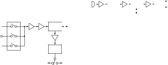
■ From antenna to a preamplifier (Q153, 154)
There are two antenna terminals: ANT 1 and ANT 2. With these antenna terminals, it is possible to select the terminal to be used and store the selection for each band. A pigtail wire is used in this transceiver to maintain the freedom of the antenna wire when it is mounted in a car.
The receive signal sent from the antenna terminal enters the ANT section (X45-366 C/3 : 200W transceiver, X45-365 C/ 3 : 100W transceiver) of the final unit. The signal passes through a surge trap, the antenna changeover relay, the antenna tuner changeover relay (only 100W transceiver), the transmission/reception changeover relay, and an image filter, and is then sent from CN503 to CN2 of the RF unit (X44-327) though a co-axial cable.
The signal input into the RF unit passes through the attenuator circuit, the image filter, the surge absorption limiter, and then enters the RF BPF. Although the default of the attenuator is 12dB, it can change to approximately 20dB by removing the CN4 jumper.
The RF BPF divides in the range as shown in table 3. The transmit signal also passes through the RF BPF when transmitting.
The preamplifier (Q153, 154) receives the signal passed through the RF BPF. This transceiver obtains necessary gain and frequency characteristic by applying NFB (Negative Feedback) to the source earthed circuit having two parallelconnected MOS FETs. Although the preamplifier was conventionally switched by switching between low-band and high-band, this transceiver can obtain necessary characteristics for each band by switching the NFB amount of the source at Q155.
You can turn the preamplifier ON/OFF by pressing the [ATT/PRE] key.
Band |
Filter range |
|
|
BC |
30kHz~1.705MHz |
|
|
1.8MHz |
1.705~2.5MHz |
|
|
3.5MHz |
2.5~4.1MHz |
|
|
7MHz |
4.1~7.5MHz |
|
|
10MHz |
7.5~10.5MHz |
|
|
14MHz |
10.5~14.5MHz |
|
|
21MHz |
14.5~21.5MHz |
|
|
28MHz |
21.5~30MHz |
|
|
|
30~49MHz, 54~60MHz |
|
|
50MHz |
49~54MHz |
|
|
Table 3 RF BPF
5
TS-480HX/480SAT
CIRCUIT DESCRIPTION
■From receiving 1st mixer to the second IF frequency (10.695MHz)
The output signal sent from the RF BPF passes through the image filter and is converted to the first IF frequency (73.095MHz) at the first receiving mixer (Q156, 157, 160, 161). The receiving first mixer has a circuit having quadruple JFETs (Q156, 157, 160, 161). This same type of circuit is used in high-class transceivers. Therefore, this transceiver has the same or higher dynamic characteristics as high-class transceivers.
Two MCF (XF151) with 2-poles are used in the next stage. This transceiver reduces proximity spurious components of
ANT1 |
ANT2 |
Filter unit (C/3) RF unit |
|
|
|
|
ANT section |
|
|
|
|
the transmit signal by passing the narrow-band MCF. It also reduces spurious components of the receive signal.
TP1 (CN152) and TP2 (CN252) adjust MCF. The signal passed through the MCF is amplified at the first IF amplifier (Q253) and converted to the second IF frequency (10.695 MHz) at the second receiving mixer (D256). The receiving second mixer is the passive type mixer using diodes and the transmit signal passes through it when performing transmission.
The second IF signal (10.695MHz) is sent from CN254 of the RF unit (X44-327) to CN501 of the TX-RX unit (X57-663 A/ 2) through a co-axial cable.
|
Except 200W |
RX |
ATT |
RF BPF |
|
|
|||
|
|
|
–12dB/ |
30kHz~ |
|
|
TX |
–20dB |
60MHz |
|
|
|
|
|
|
AT |
TX |
|
|
|
|
|
|
|
|
|
signal |
|
|
|
|
|
Through |
Q153,154 |
|
|
|
PRE AMP OFF |
PRE AMP |
|
D256 |
|
Q253 |
|
10.695MHz |
RX 2nd Mixer |
1st IF AMP |
Q156,157,160,161 |
|
|
|
|
||
RX 2nd IF |
|
|
MCF |
|
|
|
RX 1st Mixer |
||
to TX-RX (A/2) |
|
|
||
|
XF151 |
|
||
|
Q255 |
|
Q159 |
|
|
|
73.095MHz |
||
|
LO2 AMP |
|
|
LO1 AMP |
|
LO2 |
|
AGC |
LO1 |
|
62.4MHz |
73.125~133.095MHz |
||
Fig. 3 From antenna to the second IF frequency (10.695MHz)
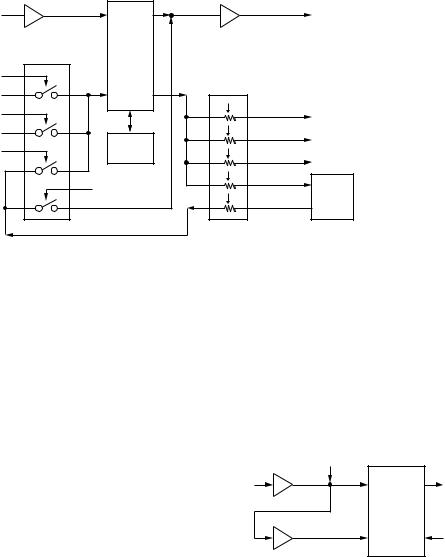
■10.695MHz IF filter circuit (Filter section (X57-663 B/2) of the TX-RX unit)
The TX-RX unit (X57-663 A/2) comprises the receiver circuit, the PLL circuit, the transmitter circuit (from AF to the first IF: 10.695MHz), the AF DSP, and the control circuit.
The second IF signal (10.695 MHz) input into CN501 of the TX-RX unit (X57-663 A/2) enters CN901 of the filter section (X57-663 B/2). This unit has the 10.695MHz IF filter and the IF amplifier. It is possible to remove the unit to mount a optional IF filter (two pieces) and TCXO (SO-3).
The second IF signal (10.695MHz) input from CN901 is amplified at the second receiver IF amplifier (Q901). The second receiver IF amplifier operates as a gate of the noise blanker. Q902 and Q901 turn OFF while blanking. Q901 amplifies the transmit signal.
The output signal sent from Q901 passes through the 10.695MHz IF filter and is amplified at the IF amplifier (Q971), then returns to the TX-RX unit (X57-663 A/2) from CN971.
Table 4 shows the path of the 10.695MHz IF filter mode. You can mount two IF filters from the following optional IF
filter types:
SSB NARROW: 1.8kHz, CW: 500Hz, and CW NARROW: 270Hz.
The option filter is automatically selected by the resistance, which is set in the option filter. Therefore, you do not need to select the filter using menu or a switch.
Filter |
Bandwidth |
RX |
TX |
|
|
|
|
Through (R943, 945) |
Through |
FM |
Not used |
|
|
|
|
XF931 |
6kHz |
AM |
AM |
|
|
|
|
XF932 |
2.4kHz |
SSB/CW/FSK |
SSB/CW/FSK |
|
|
/AM NAR |
/FM |
|
|
|
|
Option filter 1 |
*1 |
*2 |
Not used |
|
|
|
|
Option filter 2 |
*1 |
*2 |
Not used |
|
|
|
|
*1: The bandwidth of the mounted IF filter is applied.
*2: The mode changes corresponding to the mounted IF filter. The CW filter is available in SSB mode with the selection is in the menu.
Table 4 IF filter selection
6
TS-480HX/480SAT
CIRCUIT DESCRIPTION
|
RF unit TX-RX unit (A/2) |
TX-RX unit |
D932 |
|
FM |
|
|
|
|
|
|
|
|||||||||||||||
|
|
|
|
|
|
|
|
(B/2) |
D940 |
through |
|
|
|
|
|
|
FM IF |
||||||||||
|
|
|
|
|
|
|
|
Filter section |
|
|
|
|
|
|
|
|
|
|
|
|
|||||||
|
|
|
|
|
|
|
|
D932 |
|
|
|
|
|
|
|
|
|
10.695MHz |
|||||||||
|
|
|
|
|
|
|
|
|
|
|
|
|
|
|
|
|
|
|
|
|
|
|
|
||||
|
|
|
|
|
|
|
|
|
|
|
|
|
|
|
XF931 |
D934 |
|
|
|
|
|||||||
|
|
|
|
|
|
|
|
|
|
|
|
|
|
|
D941 |
|
|
|
|
||||||||
|
|
|
|
|
AGC |
|
|
|
|
|
|
|
|
|
|
|
|
|
|
|
|||||||
|
|
|
|
|
|
|
|
|
|
|
|
|
|
|
|
|
|
|
|
|
|
|
|
|
|
||
|
|
|
|
|
|
|
|
|
|
|
|
|
|
|
|
|
|
|
|
|
|
|
|
|
|||
|
|
|
|
|
|
|
|
|
|
|
|
|
|
|
|
|
|
|
|
|
|
|
|
|
|
|
|
|
|
|
|
|
|
|
|
|
Q901 |
|
|
|
|
|
|
AM 6kHz |
|
|
|
|
Q971 |
||||||
|
|
|
|
|
|
|
|
|
|
|
|
|
|
|
|
|
|
|
|
|
|
||||||
|
|
|
|
|
|
|
|
IF AMP |
|
|
|
D931 |
XF932 |
D936 |
IF AMP |
||||||||||||
|
2nd IF |
|
|
|
|
|
|
|
|
|
|
|
|
|
|
|
|
|
|
|
RX OUT |
||||||
|
|
|
|
|
|
|
|
|
|
|
|
|
|
|
|
|
|
|
|
|
|
|
|
|
|
||
|
|
NB IN |
|
|
|
|
|
|
|
|
|
|
|
|
|
|
|
|
|
|
|
10.695MHz |
|||||
|
|
|
|
|
|
|
|
|
|
|
|
|
|
|
|
|
|
|
|
|
|
||||||
10.695MHz |
|
Q508 |
NB |
|
|
|
SSB/CW/FSK 2.4kHz |
|
|
|
|
||||||||||||||||
|
|
|
|
|
|
|
|
|
|
|
|
|
|
|
|
|
|
|
|
|
|||||||
|
|
|
|
|
|
|
|
|
|
|
D933 |
|
|
|
D935 |
|
|
|
|
||||||||
|
|
|
|
|
Noise |
|
|
gate |
|
|
|
|
|
|
|
|
|
|
|||||||||
|
|
|
|
|
|
|
|
|
|
|
|
|
|
|
|
|
|
|
|
|
|
|
|
|
|
||
|
|
|
|
|
blanker |
|
|
|
|
|
|
|
|
|
|
|
|
|
|
|
|
|
|
|
|
|
|
|
|
|
|
|
|
|
|
|
Q902 |
|
|
|
Option |
|
|
|
|
|
|
|
|||||||
|
|
|
|
|
|
|
|
|
|
|
|
|
|
|
|
|
|
|
|||||||||
|
|
|
|
|
|
|
|
|
SW |
D933 |
|
filter 1 |
D935 |
|
|
|
|
||||||||||
|
|
|
|
|
|
|
|
|
|
|
|
|
|
|
|
|
|
|
|
|
|
||||||
|
|
|
|
|
|
|
|
|
|
|
|
|
|
|
|
|
|
|
|
|
|
||||||
|
|
|
|
|
|
|
|
|
|
|
|
|
|
|
|
|
|
|
|
|
|
|
|
|
|
|
|
|
|
|
|
|
|
|
|
|
|
|
|
|
|
|
|
|
|
|
|
|
|
|
|
|
|
|
|
Option
filter 2
Fig. 4 10.695MHz IF filter circuit
■From the receiver second IF to detection (TX-RX unit (X57-663 A/2))
The path of the second IF signal (10.695MHz) input into CN555 of the TX-RX unit (X57-663 A/2) is different between FM mode and all other modes until the detection stage.
In modes other than FM mode, the second IF signal is amplified at Q551 and Q554. The diode located at the second side of the loading side coil (L553) of Q551 is a PIN diode (D551). With the current applied to the PIN diode, the receiving total gain, which is used to start the AGC operation, is determined in modes other than FM mode. It is possible to change the current with adjustment menu No.1 (AGC Ref.).
The transistor (Q561) connected to the source of Q554 is used as a switch to mute the IF signals in modes other than FM mode while transmitting.
The signal amplified at Q554 is detected at the mixer IC (IC553) and becomes the AF signal in SSB/ CW/ FSK mode.
In AM mode, the signal amplified at Q554 passes through Q556 and is detected at D555. Some DC bias is applied to D555 to reduce distortion of small signals. The output signal D552 sent from Q556 is rectified at D552 and the AGC voltage is generated by Q552.
In FM mode, the second IF signal enters into the FM IC (IC551). The entered signal is converted to 455kHz. The signal is then amplified at the limiter circuit in the FM IC, where it is detected.
Although the receive bandwidth in FM mode is decided by the ceramic filter (CF551), the bandwidth of the filter does not change in FM Narrow mode.
FM IF |
|
|
|
|
|
|
10.695MHz |
|
|
|
IC551 |
|
FM |
|
|
|
|
FM IC |
|
|
D940 |
Q551 |
|
Q554 |
|
|
|
|
|
|
|
|||
RX OUT |
AGC |
D551 |
AGC |
IC553 |
|
|
AMP RX ATT AMP |
Mixer IC Q558 |
|
||||
10.695MHz |
|
|
|
|
|
SSB/CW/FSK |
|
|
|
|
|
|
|
Q971 |
IFGC |
|
|
|
|
|
|
|
|
CAR |
|
|
|
|
|
|
|
|
|
|
|
|
|
|
10.695MHz |
|
|
|
Q561 |
Q556 |
|
Q557 |
|
|
|
Mute SW |
|
|
|||
|
IF AMP |
D555 |
Buffer |
|
||
|
|
|
||||
|
|
|
|
|
|
|
|
|
|
|
|
|
AM |
TX-RX unit (B/2) TX-RX unit (A/2) Filter section
D552
 AGC
AGC
Q552
AGC AMP
Fig. 5 From the receiver second IF to detection
7
TS-480HX/480SAT
CIRCUIT DESCRIPTION
■ From detection to AF output
As for the AF signal detected in each mode, a necessary mode for the signal is selected by the analog switch (IC733). The AF signal is amplified at IC224 and IC218 and converted to a digital signal by the CODEC (IC217), and is then sent to the DSP (IC220).
In the DSP, the basic signal processing such as AF gain, the interference elimination such as slope tune, and the noise reduction such as NR are performed for the signal. The signal is then converted to an analog signal again at the CODEC.
The analog signal is amplified at IC214, then re-amplified at the AF amplifier (IC734) to drive the speaker.
To utilize the convenience of the “completely separated panel type”, the internal speaker and the headphone terminal is mounted in the panel and the external speaker terminal is mounted in the transceiver.
To realize the priority of the received audio output (the headphone (top priority), the external speaker (the second priority), and the internal speaker (the third priority)), use the headphone and the external speaker jack having a switch to make each MCU (X54 IC3, X57 IC204) recognize the condition of the inserted plug and switch the relay set on the output of the AF amplifier (IC734) in order to select an appropriate path.
IC733
Analog SW
IC218
IC224 (A/2)
FM
SSB
CW
FSK
AM
TX-RX unit (A/2)
IC217 |
|
|
|
IC220 |
CODEC |
|
|
|
DSP |
IC214
(A/2)
IC734
AF AMP
Panel
EXT. SP
(INT. SP/Headphone)
Fig. 6 From detection to AF output
Transmitter Circuit
There are two types of transmission output: 200W (TS480HX) and 100W (TS-480SAT). The 100 W transceiver has an internal antenna tuner.
With the presence of the internal antenna tuner, the final section (A/3), the LPF section (B/3), and the ANT section (C/3) of the final unit is different between the 200 W transceiver and the 100W transceiver (200W transceiver: X45-366, 100W transceiver: X45-365). The same type of the TX-RX unit (X57-663) and RF unit (X44-327) are used in both the 200W transceiver and the 100W transceiver, even though there is a small constant difference.
In addition, the same type of display unit (X54-341) is used in both the 200W transceiver and the 100W transceiver.
■ From the MIC terminal to modulation output
The frequency configuration of the transmitting part is double superheterodyne: the transmitter first IF (10.695MHz) and the transmitter second IF (73.095MHz). The same type 16-bit DSP as the receiver circuit is used in the audio signal processing stage.
The MIC terminal is mounted in the transceiver and a modular jack is also employed. This is the fist time an HF transceiver to has had a modular jack.
The AF signal input from the MIC terminal is amplified at the microphone amplifier (IC221) and passes through the analog switch (IC219), where it is amplified again at IC218. The AF signal is converted to a digital signal by the CODEC (IC217), and is then sent to the DSP (IC220).
In the DSP,. the MIC gain, the processor, and various filtering are performed for the signal and it is converted to an analog signal by the CODEC. The analog signal is amplified at IC214 and assigned to FM mode or a mode other than FM mode by the DAC: IC212 (used as the electrical volume), and is then sent to each modulation circuit.
MIC |
|
|
|
|
|
|
|
|
|
|
|
|
|
FM MOD |
||||
|
|
|
|
|
IC219 |
|
|
|
|
IC217 |
|
|
|
|
IC212 |
|
||
|
|
|
|
|
Analog |
|
|
|
|
|
|
|
|
|||||
|
|
|
|
|
|
|
|
|
CODEC |
|
|
|
|
DAC |
|
|
||
|
|
IC221 |
SW |
|
IC218 |
|
|
|
|
SSB/AM/FSK |
||||||||
|
|
|
|
|
|
|
IC214 |
|
|
|
||||||||
|
|
|
|
|
|
|
|
|
|
|
Balanced MOD |
|||||||
|
|
|
|
|
|
|
|
|
|
|
||||||||
|
|
|
|
|
|
|
|
|
||||||||||
|
MIC AMP |
(B/2) |
|
|
|
|
|
|
|
|||||||||
|
|
|
|
|
(B/2) |
|
|
|
|
|||||||||
|
|
TX-RX unit (A/2) |
|
|
|
IC220 |
|
|
|
|
|
|||||||
|
|
|
|
|
|
|
|
|
|
|
|
|||||||
|
|
|
|
|
DSP |
|
|
|
|
|
|
|
||||||
Fig. 7 From the MIC terminal to modulation output
Signal Path Before/ After the CODEC
The signal path changes corresponding to the transmission/reception since the CODEC exchanges the signal with the optional unit (VGS-1).
■ Functions relating to transmission
1) Modulation input path
The output signal sent from the analog switch (IC219) enters the CODEC, and is then sent to the DSP (IC220).
•The signal sent from the microphone is output from pin 11 to pin 10 of the analog switch.
•The signal sent from the data terminal (ANI) is output from pin 1 to pin 2 of the analog switch.
•The message output signal (DRO) sent from the optional unit (VGS-1) is output from pin 4 to pin 3 of the analog switch.
2) Modulation output path
The AF signal processed at the DSP (IC220) enters the CODEC (IC217) again and is amplified at IC214. The signal amplified at IC214 passes through the following signal paths in FM mode and SSB/ AM/ FSK mode. (The MIC gain is decided at the DSP, not DAC (IC212), in both modes.)
•FM mode
The signal enters pin 21 of the DAC, and is then sent from pin 22 to the FM modulation circuit (FMOD).
•SSB/ AM/ FSK mode
The signal enters pin 24 of the DAC, and is then sent from pin 23 to the balanced modulation circuit (SMOD).
8
TS-480HX/480SAT
CIRCUIT DESCRIPTION
3) Recording a message
The signal sent from the microphone is output from pin 11 to pin 10 of the analog switch (IC219), where it enters into the CODEC (IC217). The signal sent from the CODEC enters pin 13 of the DAC (IC212), and is then sent from pin 14 to the optional unit (VGS-1) to be recorded.
■ Constant received audio recording function
1) Recording
A part of the received audio signal is sent from the CODEC (IC217) to pin 13 of the DAC (IC212), and is then sent from pin 14 of the DAC to the optional unit (VGS-1) to be recorded. The recording level is automatically compensated to become constant and you cannot randomly change the level.
2) Playback
The output signal (VOI) sent from the optional unit (VGS-1) passes from pin 1 to pin 2 of the DAC. The signal passes from pin 8 to pin 9 of the analog switch (IC219), and is then mixed with the input signal of the AF amplifier (IC734). The DAC (IC212) controls the volume.
■ Other functions
1) Playing a message (monitor)
The output signal (VOI) sent from the optional unit (VGS-1) passes from pin 1 to pin 2 of the DAC. The signal passes from pin 8 to pin 9 of the analog switch (IC219), and is then mixed with the input signal of the AF amplifier (IC734). The DAC (IC212) controls the volume.
2) Playing a pre-recorded voice message
The above-mentioned signal path is also used for playing a pre-recorded voice message.
|
IC218 (A/2) |
DET |
|
|
|
|
|
|
|
|
|
|
|
AF OUT |
|
|
|
|
|
|
|
|
|
|
IC219 |
|
|
|
IC734 |
|
|
|
|
IC217 |
|
AF AMP |
|
|
|
|
Anolog SW |
|
|
|
|||
|
CODEC |
|
|
|
|
||
|
12 |
|
|
|
|
|
|
MIC |
|
|
|
IC212 |
|
|
|
|
|
|
|
|
|
||
MIC |
11 |
10 |
|
|
DAC |
|
|
|
|
|
|
|
|
|
|
PKD |
13 |
|
|
21 |
22 |
|
FMOD |
1 |
2 |
|
|
|
|
||
|
|
|
|
|
|||
ANI |
|
24 |
23 |
|
|
||
5 |
|
IC220 |
|
SMOD |
|||
DRO |
|
|
|
|
|||
4 |
3 |
DSP |
16 |
15 |
|
ANO |
|
|
|
||||||
DRO |
|
|
|
|
|||
|
6 |
|
13 |
14 |
DRM |
|
|
|
|
VOS |
Option |
||||
|
|
|
|
|
|||
|
8 |
9 |
2 |
1 |
VOI |
||
VOO |
VOAF |
VGS-1 |
|||||
|
|
|
|
|
|
|
|
|
|
|
VOO |
|
TX-RX unit (A/2) |
||
Fig. 8 Signal path before/after the CODEC
Modulation Circuit
The modulation signal processed at the DSP is sent to the modulation circuit. The circuit receiving the modulation signal is different between FM mode and SSB/ AM/ FSK mode.
1) SSB/ AM/ FSK mode
The modulation signal sent from the DAC (IC212) enters the balanced modulator (IC621) after inverting the phase at Q625. The 10.695MHz transmission signal sent from the balanced modulator is amplified at Q621 and is then sent to the next stage.
•AM mode
The DC voltage is applied to the pin 1 of the balanced modulator via D624. With the DC voltage, the AM carrier is generated since the balanced modulator becomes unbalanced.
•FSK mode
In conventional FSK mode, the frequency of the carrier was changed with the external keying signal. This trans-
ceiver generates the FSK signal by changing the single tone (AF) generated at the DSP. The balanced modulator performs the same operation as SSB mode.
•CW/FM mode
The necessary carrier wave is obtained by making the balanced modulator lose balance.
DC for Q625 AM/FSK (1/2)
SSB/AM/FSK Mod. IN
Differential Q625 input
(2/2)
TX-RX unit (A/2)
DSB OUT
10.695MHz
IC621
Balanced
Mod.
CAR 10.695MHz
Fig. 9 SSB/AM/FSK mode modulation circuit
9
TS-480HX/480SAT
CIRCUIT DESCRIPTION
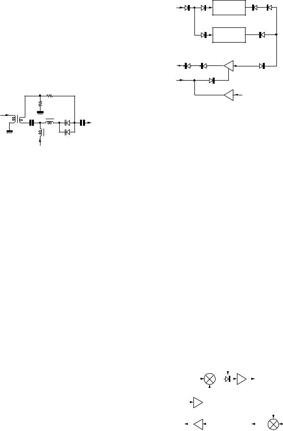
2) FM mode
Although the circuit directly modulating the frequency of the VCO and the crystal oscillator was conventionally used, this transceiver uses a phase modulation circuit.
Set the variable capacity diode (D1) on the output of the DDS (IC1) working as the source of the reference frequency of the PLL circuit generating the first local oscillator (LO1). Some DC fixed bias is applied to the variable capacity diode (D1) in order to optimise the modulation sensitivity.
Although LO2 or the crystal oscillator (10.695MHz) is modulated in the conventional transceiver, the first local oscillator (LO1) is modulated in this transceiver.
Ref. OSC |
L7 |
R31 |
R34 |
|
(31.2MHz) |
|
L11 D1 |
FM Mod. |
|
IN |
|
|
||
from Q7 |
|
|
|
OUT |
|
|
|
L10 |
to Q9 |
|
|
|
|
|
TX-RX unit (A/2) |
FM Mod. |
|
||
|
|
audio IN |
|
|
Fig. 10 FM mode modulation circuit
■ From the modulation circuit to 10.695MHz
The transmission signal sent from the balanced modulator (IC621) is sent from the filter section (X57-663 B/2) of the TXRX unit to the TXIN terminal (pin 8) of CN555. It is possible to remove the unit to mount an optional IF filter and TCXO. You can mount two optional IF filters. The IF transmit signal passes through the XF931 (passband: 6kHz) in AM mode and XF932 (passband: 2.4kHz) in modes other than AM mode.
Although various IF filters can be selected, corresponding to the passband and mode when receiving, the IF filter is automatically selected by mode when transmitting. The transmit signal passes through the 10.695MHz IF filter, is amplified at the IF amplifier (Q901), and is then sent to the IFIN terminal (pin 10) of CN554 of the TX-RX unit (A/2).
The IF amplifier (Q901) performs the gain varying operation with the ALC voltage while transmitting. The ALC voltage controls gate 2 of Q901 and the AGC voltage is applied to gate 2 while receiving. The bias voltage transferred from D905 is provided to the source of Q901 while transmitting. Q903 turns ON while receiving and it discharges TXB voltage.
The transmit signal sent from the IF amplifier (Q901) passes through D903 and D901. While D903 turns ON when transmitting, D901 makes the attenuator operate by changing the impedance with the IFGC voltage which changes the IF transmit signal. The level variance works as the TGC function controlling the transmit gain.
The 10.695MHz transmit IF signal returned from the IFIN terminal (pin 10) of CN901 of the TX-RX unit (B/2) to the TXRX unit (A/2) is sent from CN501 of the TX-RX unit (A/2) to CN254 of the RF unit (X44-327) through a co-axial cable.
TX IF IN |
D938 |
D934 |
XF931 |
D941 D932 |
|
|
|
||
10.695MHz |
|
|
BW : 6kHz |
|
|
|
|
AM |
|
|
|
D936 |
XF932 |
D931 |
|
|
|
|
|
|
|
|
BW : 2.4kHz |
|
|
|
SSB/CW/FM/FSK |
||
TX IF OUT |
D901 |
D903 |
Q901 |
D902 |
|
||||
|
|
|
|
|
10.695MHz |
|
D905 |
|
|
TXB |
|
|
||
|
|
Q903 |
|
|
|
|
|
|
|
RXB |
TX-RX unit (B/2) |
|
Filter section |
||
|
Fig. 11 From the modulation circuit to 10.695MHz
■ From 10.695MHz to the drive output
The 10.695MHz transmit IF signal input into CN254 of the RF unit (X44-327) is converted to the transmit frequency in LO1 and LO2 and sent from CN1 to the final unit (A/3) as a drive output.
The 10.695MHz transmit IF signal is converted to 73.095 MHz by LO2 (62.4MHz: 4 x 15.6MHz (the reference frequency) ) using the transmit mixer (D256). The D256 operates as a RX mixer while receiving mode.
The converted signal passes through D254 and is amplified at the IF amplifier (Q252). D254 can change the level of the 73.095 MHz transmit IF signal by changing the impedance with the current corresponding to the PGC voltage. The level variance compensates the gain of the transmit signal when performing the power control.
The 73.095MHz transmit signal passes through the MCF (XF151) and is converted to the desired transmit frequency by LO1 in the final transmit mixer (IC251). This transceiver can reduce proximity spurious components since the signal passes through the MCF (passband: approximately 15kHz) when transmitting.
The signal sent from the final transmit mixer passes through the RF BPF and is amplified at the drive amplifier (Q3) to drive the final stage, and is then sent from CN1 to the final unit (A/3).
Many spurious components can be seen when the drive output signal is analysed with the spectrum analyser. This problem occurs when the transceiver is not properly adjusted or the gain balance is not normal (when the input level to the final transmit mixer (IC251) compensating the lack of gain of the final stage is excessively high).
RF unit |
|
|
|
|
|
|
D256 |
PGC |
XF151 |
|||||||||||||
TX IF IN |
|
|
|
|
TX mixer |
|
|
|
Q252 |
|||||||||||||
|
|
|
|
|
|
|
|
|
|
|
|
|
|
|
|
|
MCF |
|
||||
10.695MHz |
|
|
|
|
|
|
|
|
|
|
D254 |
73.095MHz |
|
|||||||||
|
|
|
|
|
|
|
|
|
|
|
|
|
|
|
|
|||||||
LO2 IN |
|
|
|
Q255 |
|
|
|
|
|
|
|
|
LO1 IN |
|||||||||
|
|
|
|
|
|
|
|
|
|
|
|
|
|
|
|
|
73.125~ |
|
|
|||
62.4MHz |
|
|
|
|
|
|
|
|
|
|
|
|
|
|
|
|
|
133.095MHz |
||||
DRV OUT |
|
|
|
|
|
|
|
|
|
|
|
|
|
|
|
|
|
|
|
|||
|
|
|
|
|
|
|
|
|
|
|
|
|
|
|
|
|
|
|
||||
|
|
|
|
|
|
|
|
|
|
|
RF BPF |
|
|
|
|
|
|
|
||||
1.8~54MHz |
|
|
|
Q3 |
1.8~54MHz |
|
IC251 |
|||||||||||||||
|
|
|
|
|
|
|
|
|
|
|
||||||||||||
|
Drive AMP |
|
|
|
|
|
|
|
TX mixer |
|||||||||||||
Fig. 12 From 10.695MHz to the drive output
10
Loading...