


 Loading...
COPYRIGHTS FOR THIS MANUAL
•JVC KENWOOD Corporation shall own all copyrights and intellectual properties for the product and the manuals, help texts and relevant documents attached to the product or the optional software.
•A user is required to obtain approval from JVC KENWOOD Corporation, in writing, prior to redistributing this document on a personal web page or via packet communication.
•A user is prohibited from assigning, renting, leasing or reselling the document.
•JVC KENWOOD Corporation does not warrant that quality and functions described in this manual comply with each user’s purpose of use and, unless specifically described in this manual, JVC KENWOOD Corporation shall be free from any responsibility for any defects and indemnities for any damages or losses.
IMPORTANT NOTICES FOR SOFTWARE
The software embedded in this transceiver and the optional application software consist of a multiple number of and individual software components.Title to and ownership of copyrights for each software component is reserved for JVC KENWOOD Corporation and the respective bona fide holder.
This product employs the software component in accordance with the End User License Agreement (hereinafter referred to as the “EULA”) stipulated by JVC KENWOOD Corporation and/or the respective bona fide holder.
Access the URL below for details of the software component stipulated in the “GPL/LGPL”.
https://www.kenwood.com/gpl/
The title to and ownership of copyrights for software that may be distributed individually are reserved for JVC KENWOOD Corporation.These software shall mean the software which can be embedded in KENWOOD product memories for proper operation.Any modifying, reverse engineering, copying, reproducing or disclosing on an Internet website of the software is strictly prohibited.
A user is required to obtain approval from JVC KENWOOD Corporation, in writing, prior to redistributing this manual on a personal web page or via packet communication.Furthermore, any reselling, assigning or transferring of the software is also strictly prohibited without embedding the software in KENWOOD product memories.
COPYRIGHTS FOR RECORDED AUDIO
The broadcast content recorded in this transceiver may not be reused, except for personal use, without prior consent of the rights holder under copyright laws.
TRADEMARKS
•KENWOOD is a registered trademark of JVC KENWOOD Corporation.
•Microsoft®,Windows®, and theWindows® logo are the registered trademarks of Microsoft Corporation in the United States and other countries.
•.NET Framework is a registered trademark of Microsoft Corporation in the United States and other countries.
•IntelliMouse and IntelliPoint are registered trademarks of Microsoft Corporation in the United States and other countries.
•All other product names referenced herein are trademarks or registered trademarks of their respective manufacturers.Marks such as ™ and ® are omitted in the body text.
INDEMNITY
•JVC KENWOOD Corporation takes all appropriate measures to ensure all descriptions in this manual to be accurate; however, this manual may still contain typos and expressions that are misleading.JVC KENWOOD Corporation is entirely free from any responsibilities arising from any losses or damages caused by such typos or expressions.
•JVC KENWOOD Corporation has the right to change or improve the product specifications, etc., described in this manual without prior notice.JVC KENWOOD Corporation is entirely free from any responsibilities for any losses or damages caused by such changes and improvements.
•JVC KENWOOD Corporation is entirely free from any responsibilities for any failures, damages or losses arising from, or in connection with, use of the transceiver with or connected to any external equipment.Failures, damages or losses shall include the failures, damages or losses that may occur at the PC connected to the transceiver or in storage devices having memory area such as a USB flash drive.JVC KENWOOD Corporation is entirely free from any
responsibilities for any secondary failures, damages or losses, including but not limited to the loss or damage of data or data files stored in these memories.
•JVC KENWOOD Corporation does not warrant that quality and functions described in this manual comply with your purpose of use and, unless specifically described in this manual, JVC KENWOOD Corporation shall be free from any responsibilities for any defects and indemnities for any damages or losses.Selection and installation of any external equipment shall be done at your own risk.You are fully responsible for the use and effects of external equipment.
•JVC KENWOOD Corporation shall be free from any responsibilities for any incidental losses or damages, such as missing communications or call opportunities caused by a failure or performance error of the transceiver.
•Well aware in your mind, we cannot answer to any and all technical information associated with method of connection to, configuration for and operation of an external device and PC beyond our knowledge.
TREATMENT OF YOUR IMPORTANT DATA
There is always a risk of losing your important data by a transceiver failure, occurrence of an unforeseen contingency, erroneous operation or faulty behavior of the transceiver. The data, such as the operating information, recorded audio,
messages, configuration data, and logs, must be backed up as necessary by yourself and stored in an external storage device such as a USB flash drive.
URL AND CONTACTS OF JVC KENWOOD CORP.
The latest URL and contacts of JVC KENWOOD Corporation at the time when this manual was written are described in this manual.Due to changes of social circumstances or
the management environment, the URL and contacts of JVC KENWOOD Corporation may change from time to time.

 TABLE OF CONTENTS
01 PROLOGUE |
|
About the Release of theTS 890S................................... |
1 |
Features of theTS-890S................................................... |
2 |
02 RECEPTION CIRCUIT |
|
Receiver Configuration..................................................... |
3 |
First Mixer......................................................................... |
5 |
Roofing Filters.................................................................. |
5 |
What is a Roofing Filter?.......................................................... |
5 |
Roofing Filters.......................................................................... |
6 |
AGC Circuits..................................................................... |
7 |
Analog AGC Circuits................................................................ |
7 |
Optimization Of Gain Distribution............................................. |
8 |
Deflection of the S Meter Needle............................................. |
8 |
Noise Level.............................................................................. |
9 |
RF Gain Adjustment................................................................. |
9 |
AGC Off................................................................................... |
9 |
Noise Blankers............................................................... |
10 |
Features of the NB1 and NB2 ................................................ |
10 |
Auxiliary Circuits............................................................. |
11 |
MediumWave Band Sensitivity Risers................................... |
11 |
03 TRANSMISSION CIRCUIT |
|
IF Circuit for Clean and Stable 100W Output Power...... |
12 |
FET Final Amplifier Circuit.............................................. |
12 |
High-speed Relay-controlled AntennaTuner.................. |
13 |
Linear Amplifier Control.................................................. |
14 |
REMOTE Connector.............................................................. |
14 |
Linear Amplifier Menu Settings.............................................. |
15 |
ALC........................................................................................ |
17 |
Transmit Power Limiter........................................................... |
18 |
ALC Operation when an External Device is Connected......... |
19 |
DRVTerminal.................................................................. |
20 |
Protections..................................................................... |
21 |
SWR Protection...................................................................... |
21 |
Overcurrent Protection........................................................... |
21 |
Thermal Protection and Fan Control....................................... |
21 |
04 LOCAL OSCILLATOR CIRCUIT |
|
Local Oscillator............................................................... |
22 |
First Local Oscillator Signal.................................................... |
22 |
05 ANTENNA CONTROL CIRCUIT |
|
Signaling Paths............................................................... |
24 |
RX Antenna Feature (RX IN / RX OUT Connectors)............... |
24 |
Antenna Output Feature (ANT OUT Connector).................... |
24 |
TS-890S User Report............................................................. |
25 |
06 MPU PERIPHERAL CIRCUIT |
|
MPU Peripherals forTransceiver Control........................ |
28 |
MPU Peripherals for Application Control......................... |
28 |
MPU Peripherals for Operation Panel Control................. |
28 |
07 DSP |
|
Features ofTS-890S DSPTechnologies......................... |
29 |
DSPs and Peripheral Hardware...................................... |
29 |
Signal Processing in the IF Stage................................... |
30 |
IF-AGC................................................................................... |
30 |
AGC Quick Recovery............................................................. |
31 |
IF Filter................................................................................... |
32 |
Interference Rejection............................................................ |
34 |
Reception....................................................................... |
36 |
Demodulation......................................................................... |
36 |
AF Filter................................................................................. |
37 |
Audio Peak Filter.................................................................... |
38 |
Noise Reduction..................................................................... |
39 |
Beat Canceler........................................................................ |
42 |
Signal Processing by Morse Code Decoder........................... |
43 |
Transmission.................................................................. |
44 |
Modulation............................................................................. |
44 |
Microphone Gain Control....................................................... |
46 |
Speech Processors................................................................ |
46 |
Other Functions.............................................................. |
48 |
TX/RX Equalizers................................................................... |
48 |
Voice Guidance...................................................................... |
48 |
08 bandscope |
|
More User-friendly Bandscope....................................... |
49 |
Differences with theTS-990S as an FFT Bandscope............. |
49 |
3Types of Scope Display Modes........................................... |
49 |
Reference Level..................................................................... |
50 |
TouchscreenTuning............................................................... |
50 |
Gradation Settings................................................................. |
51 |
Tuning Assist Line, Filter Passband Display and Frequency |
|
Marker.................................................................................... |
51 |
09 SOFTWARE |
|
Display Function for Actual Operation............................. |
52 |
Meter...................................................................................... |
52 |
Transmission Digital Meter..................................................... |
53 |
Filter Scope............................................................................ |
53 |
Operability Improvements for Split Operation................. |
54 |
Split Frequency Configuration By Using the Numeric |
|
Keypad.................................................................................. |
54 |
Band Direct Key Configuration for Split.................................. |
54 |
Split Frequency Change By Using the RIT/XIT Knob............. |
54 |
Split Frequency Reception By Using an External Sub |
|
Receiver................................................................................ |
55 |

 TABLE OF CONTENTS
CW/RTTY/PSK Decoding/Encoding Available Only for the |
|
Main Unit........................................................................ |
55 |
Decoding/Encoding of CW Morse Code................................ |
55 |
Decoding/Encoding of RTTY/PSK......................................... |
56 |
Data Mode Convenient for Operation Using an External |
|
Device............................................................................ |
57 |
Switching the Input Sound Source......................................... |
57 |
USB Keying............................................................................ |
58 |
Functions Related to the Internal Memory/USB Flash |
|
Drive/File Management.................................................. |
58 |
Selection of Data Storage Location........................................ |
59 |
Storage and Reading of Configuration Data........................... |
59 |
Copying from the Internal Memory to the USB Flash Drive.... |
59 |
Copying from the Internal Memory to a PC............................. |
60 |
Configuring the Images to be Used in the Screen Saver........ |
60 |
Other Useful Functions................................................... |
61 |
Audio Scope.......................................................................... |
61 |
Recording Function................................................................ |
61 |
Clock Setting Function that uses an NTP Server.................... |
61 |
Transverse Dial Display in SWL Mode.................................... |
62 |
Firmware Updating................................................................. |
62 |
PC-Control............................................................................. |
63 |
KNS Operation without using the Host PC...................... |
65 |
Windows Software.......................................................... |
66 |
System Configurations................................................... |
67 |
NewOptionARCP-890(RadioControlProgramforTS-890S) |
|
(Free Software Application)............................................ |
70 |
Basic Specifications Inherited from the ARCP 990................ |
70 |
User Interface......................................................................... |
70 |
New Option ARHP-890 (Radio Host Program) (Free |
|
Software Application)..................................................... |
71 |
Basic Specifications Inherited from the ARHP 990................ |
71 |
User Interface......................................................................... |
71 |
ARUA-10 (USB Audio Controller) (Free Software |
|
Application).................................................................... |
72 |
Basic Functions...................................................................... |
72 |
Behavior................................................................................. |
72 |
ARVP-10H/ARVP-10R (RadioVoIP Program) (Free |
|
Software Application)..................................................... |
73 |
Basic Functions...................................................................... |
73 |
Virtual COM Port Driver.................................................. |
74 |
10 terminal FUNCTIONS |
|
ACC 2 Connector........................................................... |
76 |
DISPLAY (DVI-I) Connector............................................ |
77 |
EXT SP 8 Ω (External Speaker Jack)............................. |
77 |
KEY PAD........................................................................ |
77 |
LAN Connector............................................................... |
78 |
METER Jack.................................................................. |
79 |
PADDLE, KEY Jack........................................................ |
79 |
PHONES Jack................................................................ |
79 |
USB Connector (USB-A)................................................ |
80 |
USB Connector (USB-B)................................................ |
81 |
11 MECHANICAL STRUCTURE |
|
Internal Structure............................................................ |
82 |
Cooling........................................................................... |
83 |
Lift-up Mechanism of the Front Bases............................ |
85 |
Operability...................................................................... |
86 |
TFT Display andTouch Panel......................................... |
88 |
Main Control Knob Mechanism...................................... |
89 |
12 SP-890 |
|
Appearance and Features.............................................. |
90 |
Speaker.......................................................................... |
90 |
Built-in Passband Filter................................................... |
91 |
Speaker Input Select Switch........................................... |
91 |

01 PROLOGUE
About the Release of the TS 890S
From the TS-590 that was released in 2010 to the TS-990S in 2013 and TS-590G in 2014, we have been releasing HF transceivers for Real DX’ers where efforts were devoted to the basic reception performance, and have received very high ratings for these products.In response to a strong demand for a grade that is positioned between theTS-990S and TS-590, we started considering the idea of commercializing theTS-800 series.
Previously, popular transceivers that were released under theTS-800 series include advanced, fully-armored units that can be used in the front line under demanding conditions such as DX contests.
Models such as theTS-820 (released in 1976:IF SHIFT, ARA processor),TS-830 (released in 1980:diverse interference elimination features),TS-850 (released in 1991:up-conversion) andTS-870 (released in 1995:first amateur transceiver with IF DSP) have played an active part with each of them equipped with the latest technology of the era.They are still employed by many of the users today.
TheTS-890S, the latest addition to the glorious history of theTS-800 family, has been developed not only to complement theTS-990S andTS-590 series, but attention has also been devoted to the “basic reception performance”, which is the main interest of our customers.As a benchmark, we have aimed to develop a design that offers top-class performance in 3rd Intermodulation Dynamic Range (3rd IMDR), as well as in Reciprocal Mixing Dynamic Range (RMDR) and Blocking Dynamic Range (BDR).
To achieve this, our initial plan when designing the receiving circuit configuration was to adopt the direct sampling system in line with the current trend.However, to enable users to make use of the unit without having to worry about the issue of overflow, we decided to adopt the down-conversion system that allows the use of narrow-band roofing filters.At the same time, we have also made significant enhancements to the C/N characteristics by developing a new first local oscillator circuit, which is another key element of superheterodyne down-conversion transceivers, based on the division type that was adopted on theTS-990S.
Doing so has allowed us to achieve the following values in the measurement:3rd IMDR (110 dB), RMDR (122 dB), BDR (150 dB) (measurement when the frequency is 2 kHz detuned, receiving frequency of 14.2 MHz, MODE CW, BW 500 Hz, PRE AMP OFF).
For the IF DSP, which is protected by the impregnable front-end as suggested by these numerical values, we have developed an original AGC algorithm that enables demodulation of incoming signals using the KENWOOD tone that is non-tiring even during prolonged operation in contests.Listening to the tone is equivalent to the joy of receiving signals.
However, numerical performance is not the only criterion that determines whether a transceiver can be put into practical use.Elements related to user-friendliness, such as operability and visibility, are also important considerations.
The same 7-inch colorTFT as with theTS-990S has been employed for the bandscope.Feedback fromTS-990S users has been incorporated into a number of aspects.Some of such new features that come in handy particularly during contest operation include the auto scroll feature in the Fixed mode, straight display for waterfall in the Center mode, and highlight display for IF passband widths.
The bandscope receiver is configured using an SDR method that enables FFT processing of the entire display span, thus achieving signal processing at a faster speed compared to theTS-990S.At the same time, the bandscope receiver separately processes signals diverted from the first mixer for the incoming signal system, and this enables the use of ATT without affecting the incoming signals.
In terms of operability, we have exercised our ingenuity in the split-operation settings so as to maximize the operational efficiency during simplex reception viaVFO A/B.These creative efforts allow configuration of the split settings using the long-press of the [SPLIT] key and the press of the numeric keypad, band change while retaining the split settings, and TXVFO operation using the [RIT/XIT] knob.Also, connection with an external receiver can be established easily using the ANT OUT feature.To use theTS-590 series as the external receiver, frequency transfer and standby are possible simply by connecting two cables.
As withTS-990S, the Digital mode comes with PSK/FSK decoding/encoding features and communication using the main unit alone is possible by connecting a USB keyboard.Not only so,TS-890S also comes with a decode/encode feature in the CW mode (only available in western languages).Morse codes can also be transmitted directly from the keyboard in the CW mode, which enables paddle-less operation.
The transmission output of 100W is the same as the conventionalTS-800 series models, butTS-890S allows for quiet and stable prolonged use with the employment of a large die-cast chassis and 80 mm x 80 mm twin fan system. Needless to say, the fans will not operate when only reception is in progress.
1

01 prologue
As described above,TS-890S has been developed to inherit the DNA of KENWOOD’s HF transceivers and as a model that forms the core of theTS-x90 series.It is an advanced transceiver for practical use that has evolved in its own ways as a full-fledged successor of theTS-800 family, and not just a modified version of theTS-990S orTS-590 models.
This in-depth manual is written by theTS-890S designers to describe the technologies and techniques used to achieve the performance and features mentioned above.We hope it will help you gain an in-depth understanding of theTS-890S.
Features of the TS-890S
•Advanced-level transceiver designed for practical use that surpasses the basic reception performance of models in the same class, boasts diverse features and inherits the texture of theTS-990S
•Adopts a 7-inchTFT color display and offers various information for an enhanced experience in the integrated management of operations:Auto Scroll mode, filter scope,TX digital meter, etc.
•Top-class basic reception performance - covers all frequency bands with the down-conversion system Comes equipped with 15 kHz, 6 kHz, 2.7 kHz and 500 Hz roofing filters (270 Hz roofing filter is available as an optional item)
•HF band, +50 MHz band, +70 MHz (European model only)
•100W heavy-duty output (50W/70 MHz for European model)
•Built-in auto antenna tuner (relay system, high-speed matching)
•SSB, CW, FSK (RTTY), PSK31 (BPSK/QPSK), PSK63 (BPSK), AM, FM
•Enables decode/encode in FSK, PSK31/63 as well as CW mode
•Two 32-bit floating-point DSPs for transmission/reception and scope display
•Equipped with LAN, USB and COM ports
•Supports external connections (DVI-I terminal)
•Supports remote control operation that does not require the use of a host PC (direct IP connection) Radio control program (ARCP890) and radio host program (ARHP-890) are supplied as free software as with previous models
•Supports USB audio PC speakers and microphone can be used for operation by employing the USB Audio Controller (ARUA-10) free software
•SP-890 (external speaker) andYG-82CN-1 (270 Hz CW filter) are available as optional items
2

02 RECEPTION CIRCUIT
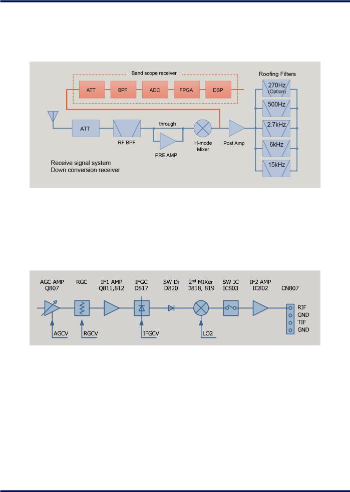
Receiver Configuration
TheTS-890S is the single-band transmitter-receiver of the down-conversion method, which is refined and diverted from the circuit configuration of the main band receiver of the top-modelTS-990S.During transmission, the receiver behavior stops.Also, the bandscope circuit shows the status of IF signals during reception and transmission.
It is important for a receiver to eliminate interfering signals through narrow filters at an earlier stage and pass desired signals to the later circuits.In addition to the RF bandpass filter placed in the front-end block of the receiver, eliminating the adjacent interfering signals by using the IF bandpass filters with better selection characteristics prevents distortion from occurring in the later circuits and improves practical anti-interference characteristics.The first mixer, through which a number of interfering signals pass, needs to have high intercept point (hereinafter referred to as IP) characteristics.
The down-conversion method where the first IF signal is 8.248 MHz is adopted.The use of a low IF signal realizes the bandpass filters with steep attenuation characteristics, and performance sufficiently tolerant to adjacent interfering signals is secured.
Next is the bandpass filters placed in the front-end block.The use of a low first IF signal allows reception interference and/or spurious reception by image frequencies to easily take place, thus it is necessary to place a number of bandpass filters with steeper attenuation characteristics.As shown in the table “Bandpass Filter Division in the Receiver”, the bandpass filters divided into multiple paths are designed to implement the high Q value and a coil with distortion resistance characteristics.
Table 1 Bandpass Filter Division in the Main Band Receiver
Band |
Filter Bandwidth |
135 k |
30 k to 521.999 kHz |
BC |
522 k to 1.704 999 MHz |
1.8 M |
1.705 M to 2.499 999 MHz |
3.5 M |
2.5 M to 4.099 999 MHz |
5 M |
4.1 M to 5.999 999 MHz |
7 M |
6.0 M to 7.499 999 MHz |
10 M |
7.5 M to 10.499 999 MHz |
14 M |
10.5 M to 14.499 999 MHz |
18 M |
14.5 M to 18.499 999 MHz |
21 M |
18.5 M to 22.499 999 MHz |
24 M |
22.5 M to 27.499 999 MHz |
28 M |
27.5 M to 34.999 999 MHz |
35 M |
35.0 M to 41.499 999 MHz |
45 M |
41.5 M to 47.999 999 MHz |
50 M |
48.0 M to 54.999 999 MHz |
60 M |
55.0 M to 59.999 999 MHz |
60 M* |
60.0 M to 61.999 999 MHz |
65 M* |
62.0 M to 68.999 999 MHz |
70 M* |
69.0 M to 74.799 999 MHz |
*European model only
3
02 RECEPTION CIRCUIT
The received signal which was input from the antenna comes into the front-end block of the receiver through the antenna switching circuit.The bandpass filter for the selected receive band eliminates interfering signals outside the band.The received signal is amplified by a pre-amplifier and is then converted to the first IF signal (8.248 MHz) by the first H-mode mixer having high IP characteristics.
The “Block Diagram of the Front-end Circuit for the Receiver”is shown below:
Fig.1 Block Diagram of the Front-end Circuit for the Receiver
The first IF signal enters the roofing filter through the bandscope branching circuit and the post-amplifier, and the adjacent interfering signals outside the band is eliminated.
The “Block Diagram of the IF Circuit for the Receiver”shown below shows the circuit configuration subsequent to the roofing filters.The first IF signal routes through the AGC amplifier and the first IF amplifier to the second mixer, which converts it to the second IF signal (24 kHz/36 kHz).The second IF signal enters the DSP as the baseband signal through the second IF amplifier, and the AGC response, all-mode demodulation, and audio signal processing, etc.are done.
Fig.2 Block Diagram of the IF Circuit for the Receiver
4
RECEPTION CIRCUIT 02
First Mixer
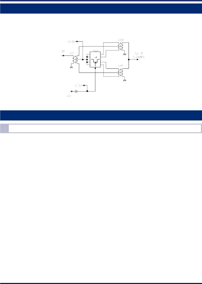
For the first mixer, the “H-mode mixer”with less distortion is refined and diverted from the one adapted in theTS-990S main receiver, and the conversion loss has been reduced and matching of the frequency characteristics of the mixer input port by the wide bandwidth is enabled.
Fig.3 First Mixer Circuit
Roofing Filters
What is a Roofing Filter?
This section describes the roofing filter, which is the most important in the receiver.The roofing filter is a filter placed at the ceiling, or the “roof”of the intermediate frequency (IF) circuit of the receiver.In other words, this represents a narrowband filter where the signal converted to the intermediate frequency first passes through.The received signals include a number of strong adjacent interfering signals other than the desired signal, thus by the attenuated amount outside the band of the filter, the signal is less likely to be distorted in the subsequent amplifying circuit.The high intercept point obtained by the high-performance first mixer gives full play to its ability in a frequency domain slightly
distant from the desired signal, which is attenuated by the roofing filter.This is why the roofing filters have been narrowed to their minimum and have been attenuated to the steepest direction.
5

02 RECEPTION CIRCUIT
Roofing Filters
Four types of roofing filters are equipped as standard as narrowband filters of high IP characteristics implemented by the full down-conversion method.In addition, to meet the needs for narrower band filters, optional filters are available (sold separately) and supported by a mounting slot.The “Photograph of Roofing Filters”is shown below:
Fig.4 Photograph of the Roofing Filters
The filters of the 15 kHz, 6 kHz, 2.7 kHz, and 500 Hz (270 Hz) bandwidth are mounted from the top in the photograph. The filters of the 15 kHz and 6 kHz bandwidth are the 4-pole monolithic crystal filters (hereinafter referred to as MCF), and the filter of the 2.7 kHz bandwidth is the 6-pole MCF.The filter of the 500 Hz bandwidth is structured as the ladder type to suppress in-band insertion losses and to steeply shape the adjacent out-of-band attenuation characteristics.The ladder filter of the 270 Hz bandwidth, which is the much narrower band, is also available as an optional filter.For each ladder filter frequency response, the “Frequency Response of the 500 Hz Bandwidth”and “Frequency Response of the 270 Hz Bandwidth”are shown below:
Fig.5 Frequency response of |
Fig.6 Frequency response of |
the 500 Hz Bandwidth |
the 270 Hz Bandwidth (Option) |
The roofing filters for the receiver can be selected regardless of the operation mode.
In the RX Filter screen which appears on the display by pressing and holding the [IF FIL] key, switching to the roofing filter corresponding to the passband width can be used for the reduction of the interference signal.
6
RECEPTION CIRCUIT 02
AGC Circuits
Analog AGC Circuits
To achieve high receive dynamic range characteristics, an analog AGC circuit is used together to make the A/D converter work to its performance limit.The AGC circuit is required to have low noise and a wide dynamic range, wide control range, and linearity to the control.TheTS-890S implements high-precision AGC response characteristics with the combination of an AGC circuit in which a dual-gate MOSFET is used and the correction process made by DSP.The “AGC Circuit with a Dual-Gate MOSFET”is shown below:
Fig.7 AGC Circuit with a Dual-Gate MOSFET
The “AGC Response Characteristics to a ControlVoltage”graph below shows the AGC response characteristics to a control voltage in the circuit configuration with a dual-gate MOSFET.Sufficient control range, dynamic range, and linearity are secured.
Response Characteristics
Fig.8 AGC Response Characteristics to a ControlVoltage
7

02 RECEPTION CIRCUIT
Optimization Of Gain Distribution
The first mixer, which is the key block in the receiver, has a large conversion loss.Therefore, a pre-amplifier to improve sensitivity is placed.
Pre-amplifier 1 is the standard behavior in a reception band below 21.5 MHz, and pre-amplifier 2 is the standard behavior in a reception band of 21.5 MHz or larger, and depending on the radio wave status, OFF / PRE1 / PRE2 can be switched by pressing the [ANT/PRE] key.
The attenuation outside the band is fully obtained by the roofing filters with good selectivity, thus even through the analog AGC amplifier and high-gain IF amplifier in a later stage, undistorted IF signals are supplied as baseband signals to the DSP.
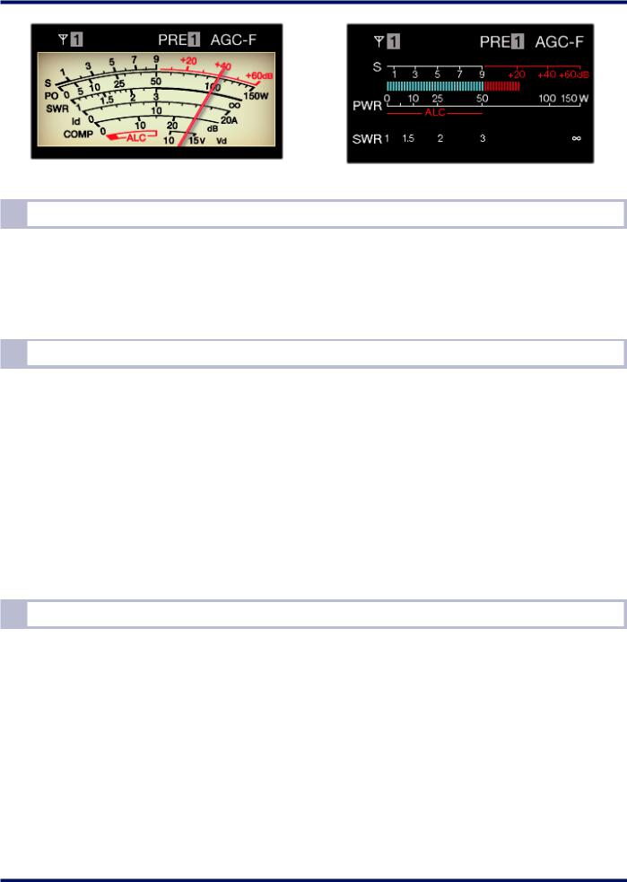
Deflection of the S Meter Needle
The IARU (International Amateur Radio Union) standard scale requires -73 dBm for S9.However, concerning the S meter needle deflection, on all of the KENWOOD transceivers, it is -81 dBm for S9 in the 14 MHz band while a preamplifier is on.TheTS-890S also provides the S meter needle deflection familiar to operators using a conventional model.
Turning off the pre-amplifiers lowers the gain and the S meter needle deflection.For the gain change by a pre-amplifier, approximately +12 dB is the standard configuration in the amateur bands up to the 21 MHz band and approximately +20 dB in the higher bands.
The “S Meter Levels”table shows the indicated levels of the S meter.(The S meter level is managed at S1, S9, or S9+60 dB in the 14 M /50 MHz band.)
In FM mode, the same deflection (Normal) as that in other mode is the default, and you can select the same high sensitivity (High) as that configured for conventional models through Menu 0-07 “FM Mode S-meter Sensitivity”
Table 2 S Meter Levels (Reference)
|
|
0.03M~21.5MHz |
21.5M 60MHz( 74.8MHz*) |
|||||
|
|
|
*Europeanmodelonly |
|
||||
|
|
|
|
|
|
|||
|
|
|
|
|
|
|
||
S-meter |
PREAMP1 |
|
|
PREAMP2 |
|
|||
|
|
|
|
|
|
|
||
|
|
AllMode |
AllMode,FMNormal |
|
FMHigh |
|||
|
|
|
|
|
|
|
|
|
|
|
Type1 |
Type2 |
Type1 |
|
Type2 |
|
Type1 |
|
|
|
|
|
|
|
|
|
S1 |
3 dot |
-107.0 dBm |
-121.0 dBm |
-114.0 dBm |
|
-141.0 dBm |
|
-116.0 dBm |
|
|
|
|
|
|
|
|
|
S3 |
11 dot |
-100.5 dBm |
-109.0 dBm |
-107.5 dBm |
|
-129.0 dBm |
|
-113.8 dBm |
|
|
|
|
|
|
|
|
|
S5 |
19 dot |
-94.0 dBm |
-97.0 dBm |
-101.0 dBm |
|
-117.0 dBm |
|
-111.3 dBm |
|
|
|
|
|
|
|
|
|
S7 |
27 dot |
-87.5 dBm |
-85.0 dBm |
-94.5 dBm |
|
-105.0 dBm |
|
-108.7 dBm |
|
|
|
|
|
|
|
|
|
S9 |
35 dot |
-81.0 dBm |
-73.0 dBm |
-88.0 dBm |
|
-93.0 dBm |
|
-106.2 dBm |
|
|
|
|
|
|
|
|
|
S9+20 |
48 dot |
-61.0 dBm |
-53.0 dBm |
-68.0 dBm |
|
-73.0 dBm |
|
-102.0 dBm |
|
|
|
|
|
|
|
|
|
S9+40 |
59 dot |
-41.0 dBm |
-33.0 dBm |
-48.0 dBm |
|
-53.0 dBm |
|
-98.5 dBm |
|
|
|
|
|
|
|
|
|
S9+60 |
70 dot |
-21.0 dBm |
-13.0 dBm |
-28.0 dBm |
|
-33.0 dBm |
|
-95.0 dBm |
|
|
|
|
|
|
|
|
|
8
RECEPTION CIRCUIT 02
Fig.9 S Meter Readout (Analog) |
Fig.10 S Meter Readout (Digital) |
Noise Level
Because a pre-amplifier has a gain, not only does the sensitivity increase with the pre-amplifier active, but the noise level rises, and the S meter needle is easily deflected.The sensitivity decreases with the pre-amplifier inactive;however, the IP characteristics improve, noise level lowers, and the S meter needle is also less likely to be deflected.In addition, the IF gain is corrected to be lowered when the pre-amplifier is turned on so that the gain, sensitivity, deflection of the S meter needle, noise level, and other factors appropriately change.
RF Gain Adjustment
KENWOOD HF-band transceivers are configured with our consistent philosophy to balance the levels, such as the sensitivity, S meter needle deflection, pre-amplifier gain, gain correction, and other factors, thus the internal noise may be conspicuous if the input level from an antenna is low.Reducing the IF gain can lower the noise level.For that purpose, the [RF] knob is provided.Rotating the [RF] knob counterclockwise reduces the IF gain and consequently lowers the noise level.Slightly lowering the gain does not change the reception sensitivity.The S meter shows the gain reduction by the AGC and the [RF] knob, thus the S meter needle deflects by the gain reduction.In the range the AGC is applicable, the S meter sensitivity does not change.
Placing the [RF] knob to the 3 o’clock position reduces the IF gain by approximately 6 dB from the maximum and reduces the noise level at no signal by approximately 6 dB.The gain reduction causes the S meter needle to deflect closer to S3.A 6 dB gain reduction causes the sensitivity to change little, and the reception sound volume does not change even with reception of a usual signal that makes the S meter needle deflect.If the noise level is noticeable, adjust the RF gain.(The S/N sensitivity does not lower until the [RF] knob is in the 12 o’clock position even when the pre-amplifier is inactive.)
AGC Off
The AGC time constants for such as the attack time, release time, and hold time are optimized for a practical radio waves state.However, for reception of a signal easily buried in noise, turning the AGC off may occasionally increase its performance.In such a case, the AGC can be disabled according to the settings screen to which the screen is switched with a long press of the [AGC] key.
With the AGC inactive, the signal level will not be controlled to be the certain volume level, and the speaker may emit very loud sounds.This is why a confirmation message appears before the AGC is turned off to prompt attention to loud sounds.
Before turning the AGC off, you must adjust the RF gain.For the signal of the S meter deflection level, rotate the [RF] knob counterclockwise to lower the RF gain level, letting the S meter needle deflect slightly wider.This prevents loud sounds from being emitted while the AGC is inactive.
If a large signal is entered while the AGC is inactive, the S meter needle deflects up to the level specified for the RF gain and the reception sound volume increases up to a certain level.However, if this level is exceeded, the reception audio volume reaches its limit and sudden distortion takes place.This is intended to set limits so that the allowable levels are not exceeded in the D/A converter and through signal processing.
9
02 RECEPTION CIRCUIT
Noise Blankers
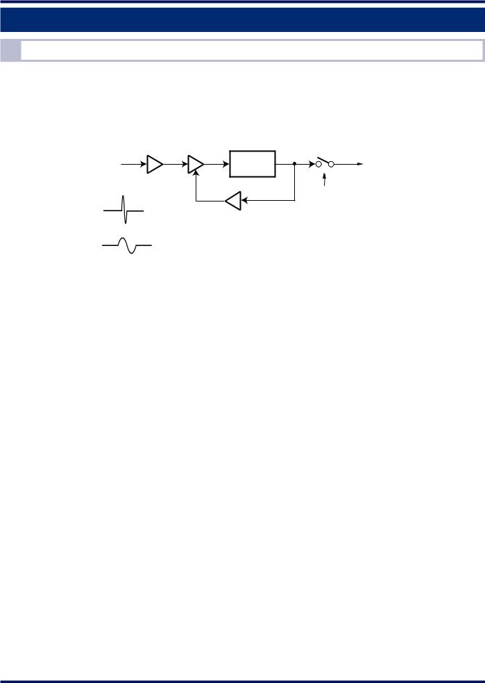
Features of the NB1 and NB2
TheTS-890S has two noise blankers;NB1 for analog processing and NB2 for digital processing by DSP.
NB1 is effective for short-cycle pulses, such as ignition noise.NB2 is effective for noise that the analog noise blanker (NB1) cannot follow.The diagram “Noise Blanker Circuit (NB1) Block Diagram”is the block diagram of the analog noise blanker (NB1).
|
Buffer Amp Noise Amp |
Mute |
|
IF Input |
Noise |
||
Detection |
Signal |
||
|
|||
|
|
Threshold |
|
1 |
|
voltage |
|
NB AGC AMP |
|
||
|
|
2
Fig.11 Noise Blanker Circuit (NB1) Block Diagram
NB1 has the circuit configuration inherited from that of conventional models, which is effective for weak noise.A pulse signal after passing through a narrowband filter changes its noise waveform, increasing the pulse width.Thus, at the roofing filter input stage, which is not subject to influence of pulse noise, signals are picked up and switch circuits operate.
For example, if a pulse with a short cycle is entered as shown in diagram 1, the AGC in the noise blanker circuit does not react to it, thus the switch functions and a muted signal will be present.
To the contrary, if a pulse with a long cycle is entered as shown in diagram 2, the AGC reacts to it and corrects the gain, thus the switch does not function and the signal will not be muted.
The adjustment of the NB1 effect can be adjusted by the value displayed on the setting screen by a long press of the [NB1] key.The larger the value, the larger the effect on noise.
As described above, the noise blanker may insufficiently take effect if the roofing filter bandwidth is narrow.However, the DSP digital noise blanker (NB2) may be unexpectedly effective in CW mode even in a bandwidth of 500 Hz or lower. This is because NB2 operates flexibly, conforming the blanking time to the pulse length.
NB2 produces an effect on the acquisition of a weak desired signal that is buried in the noise with a long pulse width that NB1 cannot eliminate.Chapter 6 DSP describes the details of NB2.
●●How to Use the NBs and NRs
There is a term:“NB cross-modulation”.This means the state in which a noise blanker is behaving with the desired signal or adjacent signal falsely recognized as a noise pulse.It does not relate to the front-end performance.
There are 2 states:the noise of non-desired signals clearly appears (or noise clearly appears according to the keying in CW), or the desired signal is heard with distortion.
The former case is caused by the noise blanker being unable to produce an effect when the desired signal is relatively strong, or when a strong signal appears in an adjacent frequency.This is because a strong signal activates the AGC of the noise blanker so that the noise amplifier gain decreases.If the level of the signal and the level of the pulse noise are equivalent, placing an attenuator or disabling the pre-amplifier decreases the front-end gain and may restore the effect of the noise blanker.
The latter case may easily take place by increasing the noise blanker level.This is a trade-off and is inevitable.If the received signal appears to be distorted, turn off the noise blanker and check the received sound.If doing so takes effect, then turning on the noise blanker and adjusting the noise blanker level is recommended.
10
RECEPTION CIRCUIT 02
Auxiliary Circuits
Medium Wave Band Sensitivity Risers
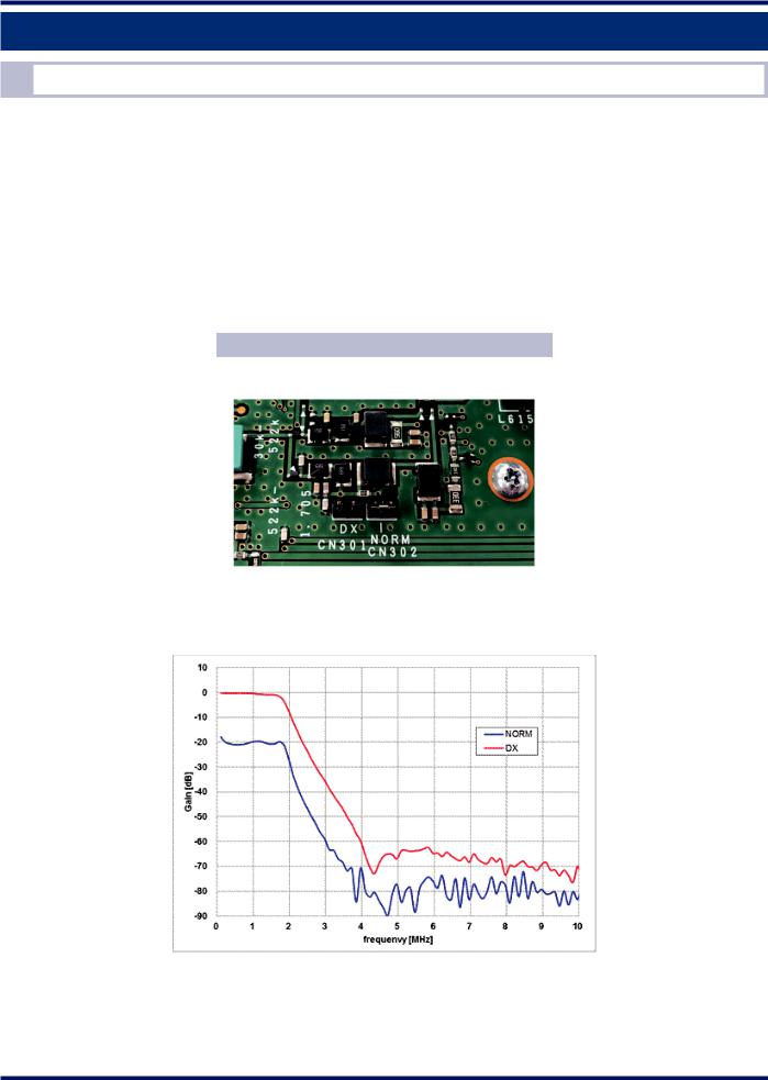
Just as in past transceivers, theTS-890S has attenuators of approximately 20 dB for the medium wave band (522 kHz to 1.705 MHz) (as the factory default, the sensitivity is lowered by approximately 20 dB by the attenuators).In the medium wave band, there are a number of strong radio waves and there may be medium wave band signal input that is excessive for low-band antennas.The inserted attenuators are intended for clear reception with no distortion even if such strong medium wave band signals are received.The signal can bypass the attenuator after switching the jumper pins on the board so as to allow the sensitivity to increase.
The image “Jumper Pin Locations”is the image of theTX-RX unit board with the main band attenuator jumper pins placed.Detach theTS-890S lower case to access theTX-RX unit.(Before detaching the lower case, be sure to first detach the upper case.There is the danger of the cases being damaged.)
Table 3 MediumWave Band ATTs
NORM ATT:20dB |
DX:Thru |
CN 302 |
CN 301 |
|
|
Fig.12 Jumper Pin Locations
The jumper pins are placed in the “NORM”position at shipment.Switching the jumper pins to “DX”bypasses the attenuators and raises the medium wave band sensitivity by approximately 20 dB.
Fig.13 MediumWave Bandpass Filter Characteristics
11
03 TRANSMISSION CIRCUIT
IF Circuit for Clean and Stable 100 W Output Power
A signal modulated and multifariously processed in the DSP is fed as the 24 kHz (modes other than FM) or 36 kHz (FM mode) transmit first IF signal by a D/A converter, which is then converted by a diode mixer used for both transmission and reception to 8.248 MHz.The second IF signal of 8.248 MHz passes through an IF filter with a 6 kHz (modes other than FM) or 15 kHz (FM mode) bandwidth at which undesired frequency components outside the band are attenuated, after which it is being amplified.
Next, the signal goes through a gain control circuit that corrects the gain difference by band, enters the mixer IC, and is then converted to a 71.752 MHz or 41.752 MHz (European model 70 MHz band only) third IF signal.After that, the signal passes through a gain control circuit that corrects the signal gain to the required level for the specified transmit power.The signal then passes through a filter that eliminates unwanted spurious components and an ALC circuit that controls the signal for stable transmit output, and enters a mixer circuit for conversion to the desired transmit frequency. Also, fine gain control is performed according to the situation, such as lowering the amplifier gain when there is no keydown during operation in the CW mode.Processing in this way enables low-noise and high-quality transmit signals to be obtained.
The signal converted to the desired transmit frequency passes through a bandpass filter to eliminate spurious signals, so as not to generate an interfering signal outside the transmit bandwidth, and is amplified to a certain level and sent to the final circuit.The drive signal generated through the process is also available from the DRV terminal (if the DRV output is enabled).
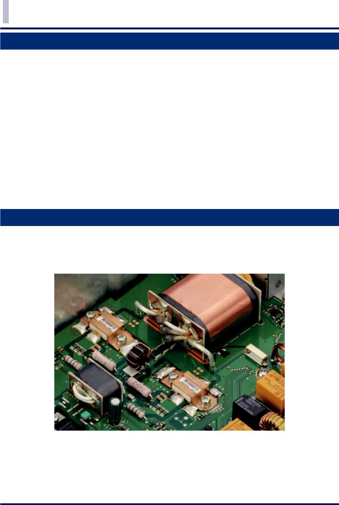
FET Final Amplifier Circuit
The final amplifier uses two MOS FET RD100HHF1 (Pch 176.5W) manufactured by Mitsubishi and is configured with a push-pull system.Meanwhile, MOS FET RD16HHF1 is employed for the drive amplifier and MOS FET RD06HHF1 for the pre-drive amplifier.Optimization of matching is performed to achieve a 13.8V final circuit with low-distortion signal.
Coupled with heat dissipation by the large die-cast, stable continuous operation can be achieved.
12
TRANSMISSION CIRCUIT 03
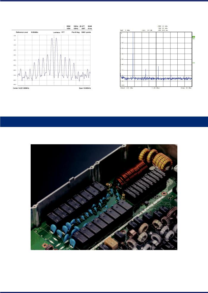
The “Transmit IMD Characteristics (14.2 MHz, 100W output power)”and “Transmit Spurious Response (14.2 MHz, 100 W output power)”graphs show the IMD characteristics and harmonic spurious response.The graphs prove superb antidistortion characteristics and clean output power.
Fig. 14 Transmit IMD Characteristics (14.2 MHz, 100W |
Fig. 15 Transmit Spurious Response (14.2 MHz, 100W |
output power) |
output power) |
High-speed Relay-controlled Antenna Tuner
TheTS-890S has a high-speed relay-controlled antenna tuner, which digitally controls in a combination of capacitors of different capacitance through switching relays.The digital control achieves high-speed tuning.
13
03 TRANSMISSION CIRCUIT
Linear Amplifier Control
Linear amplifier control can be used for switching between transmission and reception of devices such as the linear amplifier and transverter.
REMOTE Connector
The REMOTE connector is a 7-pin DIN type connector, the same as our conventional transceivers.
The LKY (Linear amplifier Keying) terminal (pin 7) is equipped with a logic to output 12V on transmission and a logic for short-circuiting to ground on transmission according to the linear amplifier menu setting which will be described later.
The “REMOTE Connector Pin Assignment”illustration shows the signaling paths allocated to the REMOTE connector pins.
REMOTE Connector (View from Rear Panel)
(RX) |
|
COM |
|
BRK |
|
(TX) |
MKE |
5 |
|||
|
4 |
2 |
|
||
|
|
|
|
|
|
|
1 |
|
|
|
3 |
ALC |
|
6 |
|
7 |
LKY |
|
10Ω |
|
GND |
||
|
|
|
|
|
|
GND: |
ON during Active High/transmission: 12 V |
|
ON during Active Low/transmission: “L” |
||
Connect to metal shield. |
10Ω
Fig. 16 REMOTE Connector Pin Assignment
Table 4 Terminal Descriptions for the REMOTE Connector
Terminal |
Terminal |
Function |
Input/ |
|
No. |
Name |
Output |
||
|
||||
1 |
SPO |
Speaker out |
O |
|
|
|
|
|
|
2 |
COM |
Common terminal of the built-in relay for linear amplifier control |
I/O |
|
|
|
|
|
|
3 |
SS |
PTT input |
I |
|
• Sends signal by grounding the SS terminal. |
||||
|
|
|
||
|
|
Make terminal of the built-in relay for linear amplifier control |
|
|
|
|
• The make terminal can be connected to the common terminal during transmission |
|
|
4 |
MKE |
by configuring “ Internal Relay Control ” of the linear amplifier menu. |
I/O |
|
|
|
Rated control capacity of relay contact: 2 A/ 30 V DC (resistance load) |
|
|
|
|
Maximum allowable voltage of relay contact: 220 V DC, 250 V AC |
|
|
|
|
Break terminal of the built-in relay for linear amplifier control |
|
|
|
|
• The break terminal can be connected with the common terminal when the latter is |
|
|
5 |
BRK |
not connected to a make terminal. |
I/O |
|
|
|
Rated control capacity of relay contact: 2 A/ 30 V DC (resistance load) |
|
|
|
|
Maximum allowable voltage of relay contact: 220 V DC, 250 V AC |
|
|
|
|
ALC input from the linear amplifier |
|
|
6 |
ALC |
• This is a negative input. The ALC circuit starts to operate from an input of |
I |
|
|
|
approximately -4 V (which can be changed from the Linear Amplifier menu). |
|
14

|
|
TRANSMISSION CIRCUIT 03 |
||
|
|
|
|
|
Terminal |
Terminal |
Function |
Input/ |
|
No. |
Name |
Output |
||
|
||||
|
|
Linear amplifier control output |
|
|
|
|
• The output logic during transmission can be configured using “ Keying Logic ” (16- |
|
|
|
|
14) of the linear amplifier menu. |
|
|
|
|
“Active High” : Outputs DC 12 V during transmission. The maximum output current is |
|
|
7 |
LKY |
100 mA. |
O |
|
|
|
“Active Low” : Switches to the “L” level (GND and short) during transmission. When |
|
|
|
|
an external bias is applied while receiving is in progress, the signal switches to the “H” |
|
|
|
|
level. Voltage and current not higher than DC 50 V and 100 mA respectively can be |
|
|
|
|
controlled. |
|
|
TheTS-890S linear amplifier control relay functions on transmission if “Internal Relay Control”is enabled in the Linear Amplifier Menu.
The linear amplifier control relay assumes that theTL-922 (discontinued) is standing by and can be connected as-is to theTL-922.For a linear amplifier that stands by with a voltage application or a short-circuit to ground, disable the relay control and make it stand by using the LKY terminal as described later.
When transmission starts while the LKY terminal is set to “Active High”, the transistor switch is turned On as shown in the illustration and 12V is diverted (100 mA or less).Active High indicates that the logic is high while the circuit is active. After connecting a linear amplifier that switches the transmission operation upon detecting a voltage output, set the LKY terminal to “Active High”.
When transmission starts while “Active Low”has been configured for the LKY terminal, the FET switch is turned On as shown in the illustration and short-circuits to ground.Active Low indicates that the logic is low while the circuit is active.
The linear amplifier type that can be connected is one that switches to the transmit state while the signal pulled up by the linear amplifier is being short-circuited to ground.When such a linear amplifier is connected, configure “Active Low”for the LKY terminal.However, the amount of withstand voltage and current are not large (DC 50V or less, 100 mA or less), thus it is not possible to drive a relay in this circuit or connect those which are activated with high voltage, such as some of the evacuated-tube type linear amplifiers (e.g.,TL-922).In such a case, use relay contacts alternatively.
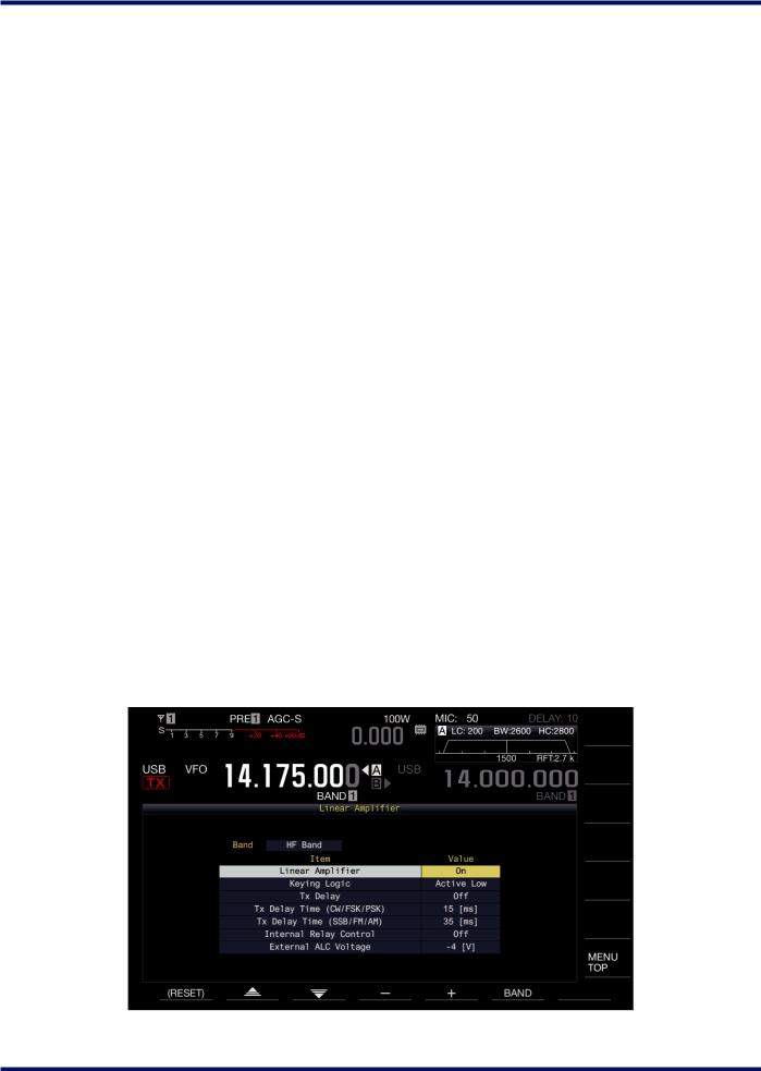
Linear Amplifier Menu Settings
The Linear Amplifier Menu is used for configuring features related to the linear amplifier. The settings are configured separately according to the band, including HF Band, 50 MHz Band and 70 MHz Band (European model only).Below are descriptions of the configurable items.
●●Linear Amplifier
Configuring to On enables the respective functions of the Linear Amplifier Menu, while the settings will not be applied when Off is selected.
●●Keying Logic
For configuring the logic for linear amplifier transmission control. Configuring to “Active High”outputs +12V during transmission. Configuring to “Active Low”short-circuits to GND during transmission.
●●Tx Delay Time
Extends the duration from when the transceiver is placed in the transmit state until radio waves are output and also the duration until audio is output after returning to reception.
Large-sized relays generally tend to take time to start switching after energizing and have a long duration of time in which chattering may take place at the moment of switching.If transmission starts before the contacts switch to the transmission side, the SWR will increase until the switching finishes, thus theTS-890S activates a protection circuit to momentarily reduce the transmit power.There is also another case where contact switching to the reception side after reception starts may cause a strong clicking noise.ConfiguringTx DelayTime may help to prevent such problems.
15
03 TRANSMISSION CIRCUIT
●●Tx Delay Time (CW/FSK/PSK)
For configuring the delay time that is enabled when in the CW/ FSK/PSK non-audio mode.
●●Tx Delay Time (SSB/FM/AM)
For configuring the delay time that is enabled when in the SSB/FM/AM audio mode. This can be configured to a setting that is different from that for the non-audio modes.
When PTT is pressed, the sound that is emitted from the PTT switch as well as the operating sound of linear amplifier relay switching may sometimes be picked up by the microphone and transmitted.In such a case, the delay time can be configured to a longer duration to prevent output of unwanted radio wave transmissions.
●●Internal Relay Control
For configuring whether to activate the built-in linear amplifier control relay.
The rated control capacity of the relay contact is 2 A/30V DC (resistance load) and the maximum allowable voltage is 220V DC and 250V AC.It can be used to switch high-voltage signals such as those of a vacuum tube linear amplifier. Control of theTL-922 (terminal voltage:-140V) is possible.
●●External ALC Voltage
For use with a linear amplifier or transverter, it is possible to connect an external device to the ALC terminal (pin 6) to enable proper transmit power control.
The External ALCVoltage can be configured to -1, -2, -3, -4 (default setting), -5, -6, -7, -8, -9 or -10 (V), and the internal gain starts to decrease upon roughly reaching the preconfigured voltage.
When the linear amplifier that is being connected supports full break-in and is placed in the transmitting state when a voltage of +12V is applied, configure “Keying Logic”to “Active High”and “Internal Relay Control”to “Off”.
If the external linear amplifier that is being connected does not support full break-in and takes time to switch the internal relay contacts, such as theTS-922, configure to “Tx DelayTime (CW/FSK/PSK)”or “Tx DelayTime (SSB/FM/AM)”in the linear amplifier menu.This configuration extends the duration of time from when the transceiver is placed in the transmit state until radio waves are practically transmitted so that the linear amplifier relaying will switch and then transmit the radio waves.If full break-in is active in CW mode, the duration of time prior to a transmission is not extended.
Note that configuring to “Tx DelayTime (CW/FSK/PSK)”or “Tx DelayTime (SSB/FM/AM)”extends not only the duration of time until a transmission starts but also the duration of time until reception begins, and this helps to reduce the click noise at the moment of switching to reception.
Fig.17 Linear Amplifier Control Settings Menu Screen
16
TRANSMISSION CIRCUIT 03
Fig. 18 Tx Delay OFF Selected (Left) and 35 ms Selected (Right)
ALC
For use with a linear amplifier or transverter, it is possible to connect an external device to the ALC terminal (pin 6) to enable proper transmit power control.
The ALC signal is a signal output from an external device that shifts the voltage to the negative side (for KENWOOD transceivers) when the transmit power reaches the range to be restricted from the external device standpoint.External devices generally have voltage adjustmentVRs (variable resistors).On theTS-890S, applying a negative voltage to the ALC terminal reduces the internal gain.The operating point is described later.
As described above, the conventional method of control is by inputting ALC signals from the linear amplifier.However, this method is no longer recommended on recent transceivers.This is because excessive power is applied to the linear amplifier before ALC voltage is input from the it, and this may cause damage to the linear amplifier.Also, the protection circuit inside the linear amplifier may be activated.To prevent such excessive input, adjust the transmit power to a proper level in advance.
●●Recommended Operation
On theTS-890S, configure the maximum transmit power that can be input to the linear amplifier in advance.The ALC control in the transceiver activates at high-speed, thus it can limit the output power without receiving an ALC signal from the linear amplifier.The transmit power limiter described later is useful for this.
After the abovementioned setting is complete, apply the ALC signal of the linear amplifier to the ALC terminal of this unit.Doing so protects the linear amplifier when it has to limit the transmit power, or in cases such as when the transmit power of theTS-890S is increased by mistake.
17
03 TRANSMISSION CIRCUIT
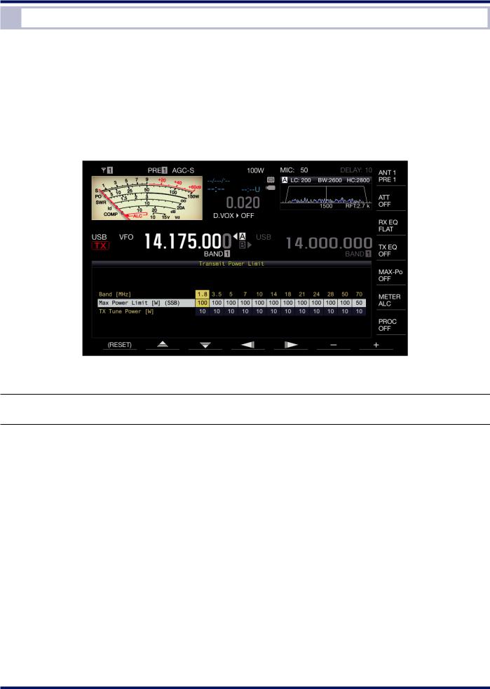
Transmit Power Limiter
The transmit power limiter prevents the transmit power from exceeding the pre-configured transmit power level.It can be turned on or off by pressing the F [MAX-Po] key.The power limit can be configured for each band as well as for each of the SSB, CW, FSK/PSK, AM/FM and DATA modes.Pressing and holding down the F [MAX-Po] key displays a Transmit Power Limit screen.Configure the transmit power on this screen.Turning the [PWR] knob clockwise continuously increases the transmit power to the preconfigured upper limit.Transmit power viaTX tuning can also be limited.
An external device such as a linear amplifier may have different gains or withstanding input powers by band, thus the required transmit power varies in most cases.Transmit power for each band can be configured on theTransmit Power Limit screen.If the maximum transmit power has been configured on the screen, this eliminates troublesome transmit power adjustment with the [PWR] knob each time the band is changed.
Fig.19 Setting Screen for the Max Power Limiter Function (E type)
Note:
Transmit power cannot be configured individually for each antenna connector (ANT1 and ANT2).
18
TRANSMISSION CIRCUIT 03
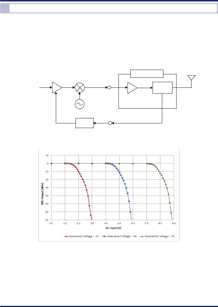
ALC Operation when an External Device is Connected
The “Connection Block to an External Device for ALC Signal Input”diagram shows the connection block with an external device when ALC signal is input from the external device to theTS-890S as well as changes in the output level with the ALC voltage.
It employs a method that controls theTS-890S gain by using an ALC voltage output from an external device, but it consequently serves to control theTS-890S transmit power.This operation is common for both linear amplifiers and transverters.The gain level of the IF circuit in theTS-890S lowers when the ALC voltage input from the external device falls below -4V (default setting).The gain decrease also leads to reduction of the transmit power (ANT output and DRV output);this serves for output control.
|
ALC AMP |
|
|
Linear Amp. etc. |
ANT |
|
TX Mixer |
DRV Terminal |
|
|
|
|
|
Detection |
|
||
TX SIGNAL |
|
|
|
||
|
|
|
|
||
|
|
|
Circuit |
|
|
|
|
|
|
|
ALC |
|
Circuit |
ALC Terminal (REMOTE Connector 6th Pin) |
|
Fig.20 Connection Block to an External Device for ALC Signal Input
Fig. 21 Changes in DRV Output Level with ALC InputVoltage
●●Operation on an ALC Signal Input from an External Device
Adjusting the microphone gain and carrier level to optimize the ALC meter needle deflection while no ALC signal is input from an external device enables more feedback control for the ALC when an external ALC signal is applied.Therefore, the increase causes the ALC meter needle to deflect wider.In this case, turn the [PWR] knob counterclockwise while monitoring the ALC meter needle deflection or readjust the microphone gain and carrier level.
19
03 TRANSMISSION CIRCUIT
DRV Terminal
The output level from the DRV connector is approximately 0 dBm (1 mW).Power detection is performed for output from the ANT terminal, and the output will not exceed the preconfigured level due to activation of ALC.However, the output level will fluctuate as ALC will not be activated for the DRV terminal output if ALC signal is not input from the external device.This output level can be configured to a level between 100% and 5% using the [POWER] knob.To decrease the output level to 5% or lower, turn the [CAR] knob in a mode other than SSB, or turn the [MIC] knob (microphone gain) or [PROC OUT] knob (speech processor output level) in the SSB mode.The level for the output signal from the DRV connector is insufficient to be transmitted directly through an antenna.Operation with a transverter or connection to the high-gain linear amplifier allows operation in the 135 kHz band and other bands.
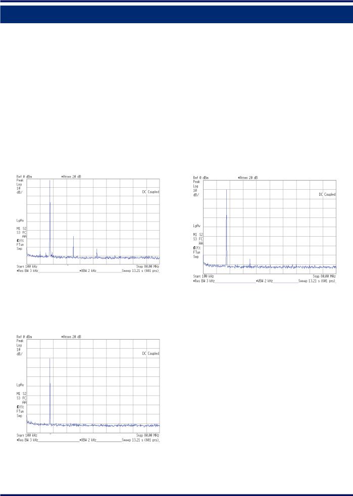
The diagram below shows the spurious characteristics from the DRV terminal in the 14 MHz band.The harmonic level also changes upon change of the level to 0 dBm, - 10 dBm, and - 20 dBm.
DRV outputs that do not pass through a low-pass filter may include a lot of harmonic components.
For transmission, eliminate such harmonic components by passing the signal through a low-pass filter as needed after signal amplification.Also, lowering the level using the [POWER] knob or applying the ALC signal from the REMOTE connector to limit the DRV connector output level can help to reduce distortion.
Fig. 22 DRV Output Characteristics 14.175 MHz 0 dBm Fig. 23 DRV Output Characteristics 14.175 MHz -10 dBm
Fig. 24 DRV Output Characteristics 14.175 MHz -20 dBm
20

TRANSMISSION CIRCUIT 03
Protections
TheTS-890S employs a final amplifier circuit configuration for a 100W transmit power output with sufficient margins. Consequently, protections against large currents and excessive heating are provided, taking account of safety
SWR Protection
Not only does a high antenna SWR impede efficient radio wave radiation, distortion may occur in the final circuit due to the reflected waves, and theTS-890S or the antennas may be damaged as a result.To prevent such a problem from occurring, a protection circuit is implemented to reduce the transmit power to reflected waves.The protection circuit starts reducing the transmit power when the SWR becomes 1.5 or higher.
Overcurrent Protection
A protection circuit is implemented to monitor currents in the final amplifier and prevent currents over a specified level from passing through.
Thermal Protection and Fan Control
TheTS-890S is equipped with two final amplifiers with thermistors placed near them.The thermistor monitors the final FET temperature and switches the rotating speed to one of the three levels based on the detected temperature. The “Cooling Fan Rotation Speeds and Final Amplifier Fan ActivationTemperatures”table shows the relationship between the speed of the cooling fan for the different components and the final amplifier temperature.If the final amplifier temperature continues to rise even while the cooling fan is running, the transmission power will be limited or transmission will be stopped and restored to the receiving state to prevent malfunction.
Table 5 Cooling Fan Rotation Speeds and Final Amplifier Fan ActivationTemperatures
FanRotationSpeed |
FinalAmplifier |
|
|
Low |
Approx.60 °C |
Medium |
Approx.70 °C |
High |
Approx.75 °C |
21
04 LOCAL OSCILLATOR CIRCUIT
Local Oscillator
The local oscillator circuit in theTS-890S is configured to obtain the characteristics needed for each signal, such as theVCO (Voltage Controlled Oscillator) division type for the first and second oscillator signals and DDS (Direct Digital Synthesizer) direct system for the third local oscillator.
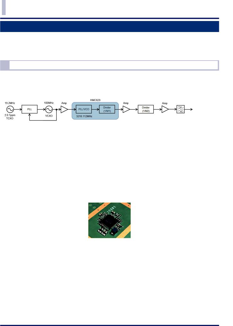
First Local Oscillator Signal
To obtain high-quality C/N (Carrier-to-Noise ratio) characteristics, the first local oscillator signal is configured by further developing theVCO division type adopted on theTS-990S to achieve aVCO device with a high C/N in the gigahertz band as well as a reference oscillator circuit that excels in adjacent C/N characteristics.
22.348 MHz
First Local Oscillator
Frequency
Fig.25 Block Diagram of First Local Oscillator Signal (Reception of 14.1 MHz Signals)
19.2 MHz reference frequency is input as the reference signal of the PLL (Phase Locked Loop) device, and the PLL loop is applied to the 100 MHz signal to generate signal with excellent C/N characteristics.
The 100 MHz signal that is generated is input to theVCO device (HMC829) to generate signal with a high C/N in the gigahertz band within the device.
The generated is then divided and passed through the amplifier and bandpass filter before it is output as the first local oscillator signal.
Theoretically, the C/N characteristics of gigahertz band signals generated inside the device are improved by the effect of division at the ratio of 20*log (division ratio).
(1/10 division:20*log (1/10) = -20dB)
Fig.26 HMC829
22
local oscillatior CIRCUIT 04
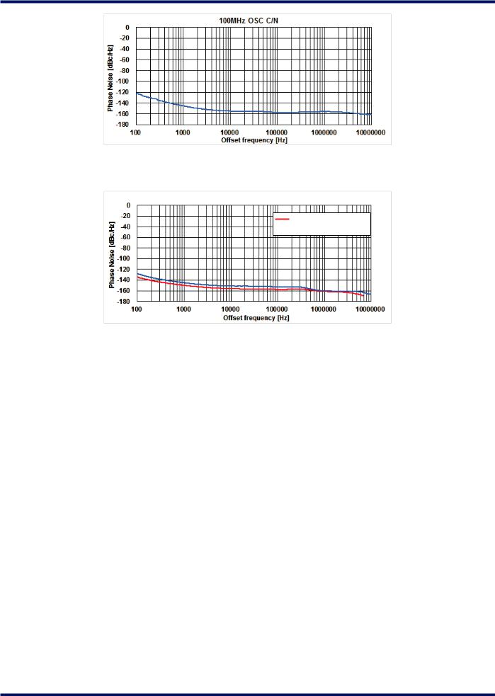
Fig.27 100 MHz OSC C/N Characteristics
First Local Oscillator Signal C/N
Reception of 14.0 MHz Signals
 Reception of 50.0 MHz Signals
Fig.28 First Local Oscillator Signal C/N Characteristics
23
05 ANTENNA CONTROL CIRCUIT
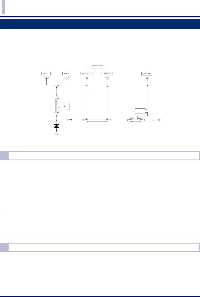
Signaling Paths
The TS-890S has two antenna connectors, ANT1 and ANT2, an RX IN and an RX OUT connector that can be used for reception-only antenna input or connection of an external filter, as well as ANT OUT connector that can be used to connect the receiver to an external device.
There are different paths that connect the antenna to the receiver.It is possible to switch the path from the antenna to the receiver by altering the settings.
BPF, etc
Splitter 3 dB loss
Fig. 29 Signaling Paths
RX Antenna Feature (RX IN / RX OUT Connectors)
The RX Antenna is a feature that receives signals via the RX IN connector or sends the received signals from the RX OUT connector when a reception-only antenna such as a low-band Beverage antenna or loop antenna is used, when a bandpass filter is appended externally, or when a transverter is connected.
When the [RX ANT] key is pressed to activate the RX antenna feature, signals from the antenna connectors (ANT1 and ANT2) are blocked, allowing reception of signals input to the RX IN connector or output of signals from the RX OUT connector.
To append an external bandpass filter, connect it between the RX OUT and RX IN connectors. However, reception is not possible if signals are not correctly input to the RX IN connector.
Note:
Install the RX antenna andTX antenna as far apart as possible.When transmitting from theTX antenna, a part of the transmit power is induced on the RX antenna.Especially when using a linear amplifier, the RX antenna generates high voltage.Note carefully that the high voltage may be applied to the RX IN connector of theTS-890S and may cause a failure.
Antenna Output Feature (ANT OUT Connector)
TheTS-890S comes with an “Antenna Output Connector”for outputting signals from the antenna to an external device.
When the [RX ANT] key is pressed and held down to activate the antenna output feature, signals from the antenna connectors (ANT1 and ANT2) can be split using a splitter circuit and the branched signals can be output to the ANT OUT connector.
In principle, the splitter circuit has a 3 dB loss.
24

ANTENNA CONTROL CIRCUIT 05
TS-890S User Report
●●Report from actual users of the TS-890S
•Dual receive with split transfer A feature
Although theTS-890S does not have a simultaneous dual-band reception feature, it can be combined with the TS-590 series or anotherTS-890S transceiver to offer a powerful dual-receive feature.While the basic operation is application of the split transfer function, the conventional split transfer feature is further expanded on the TS-890S to enable smooth operation with simultaneous reception of two bands.
There are two split transfer modes, A and B, for the transceiver pair.Between them, the newly-added split transfer A is closer to the simultaneous reception function available on models such as theTS-990S.
Transceivers that can be combined include theTS-890S series,TS-590G series andTS-590 series (only functions as a sub-receiver).When combining theTS-890S with aTS-590G model, it is also possible to configure one of them as the main transceiver.
TheTS-590 series does not have a feature for branching the output received into two, and thus cannot be configured as the main transceiver.Use an RS-232C cross cable to connect the COM ports of the two transceivers to enable mutual transfer of data.
Firmware compatibility is necessary on theTS-590 transceiver in order to use this feature on aTS-590 orTS-590G transceiver.(TS-590:Ver.2.04 or later/TS-590G series:Ver.1.05 or later)
Both theTS-890S andTS-590 series comes with a 9-pin D-sub COM port.Connect them using an RS-232C cross cable and configure the necessary items for split transfer A in the menu.
D-sub 9-pin RS-232C cross cables are sold as “interlink cables”.Connect the antenna terminal of theTS-590 with the ANT OUT terminal of theTS-890S using a coaxial cable, followed by setting the ANT OUT feature on the front panel of theTS-890S to ON.
Doing so distributes the signal from the antenna to theTS-890S unit and theTS-590.
By configuring the sub-receiver settings for split transfer A on theTS-590, transmission is prohibited automatically and therefore there is no need for manual setting to prevent inadvertent transmission by theTS-590.
Configure theTS-890S as follows.
•Menu [7-04] “Quick DataTransfer”:Select A (TX/RX)
•Menu [7-00] “Baud Rate (COM Port)”:Select 115200 [bps]
•Menu [3-12] “Split Frequency Offset by RIT/XIT Control”:SelectTX Frequency Offset while RX
Configure theTS-590 as follows.
•Menu [64]:Select A-SUB R
•Menu [67]:Select 115200 bps
Enable the split operation mode on theTS-890S and setVFO A/B.WhenTXVFO on theTS-890S is altered, the RX frequency on theTS-590G will change automatically.To change theTX frequency on theTS-890S, set XIT to ON and turn the RIT/XIT knob.Alternatively, the RX frequency of theTS-590 can be adjusted by pressing and holding down theTF-SET button and turning the main dial at the same time.When the frequency on theTS-590G is altered, this is transferred to the transmitting end of theTS-890S by pressing the Q-MIN button on theTS-590G.
25
Loading...