

Page 1
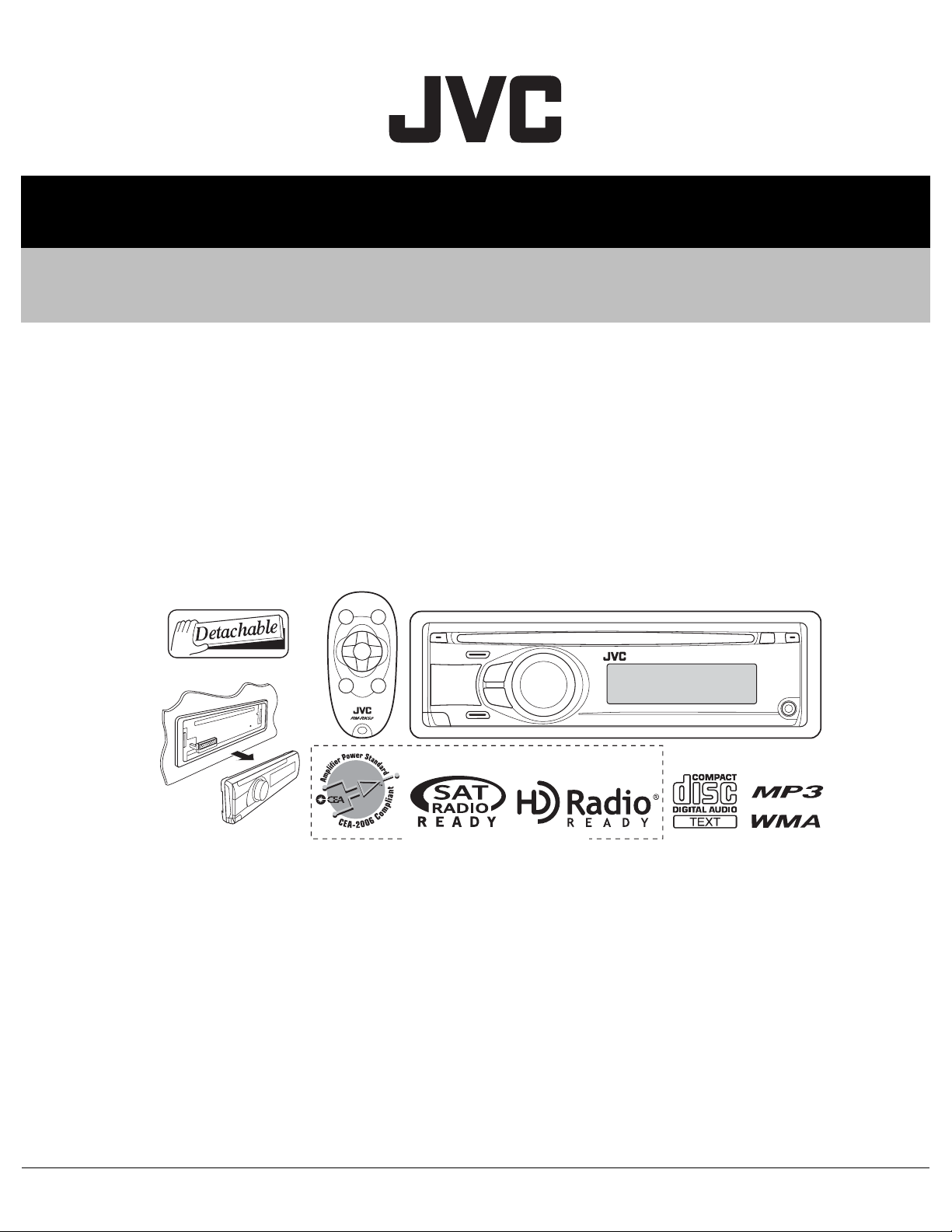
SERVICE MANUAL
CD RECEIVER
MA429<Rev.002>20098SERVICE MANUAL
KD-A305J, KD-R300J, KD-R404UI,
KD-R405U, KD-R405UN, KD-R405UT,
KD-R405UH, KD-R406U, KD-R406UN,
KD-R406UT, KD-R406UH, KD-S26J
KD-A305/KD-R300/KD-S26
COPYRIGHT © 2009 Victor Company of Japan, Limited
Lead free solder used in the board (material : Sn-Ag-Cu, melting point : 219 Centigrade)
Lead free solder used in the board (material : Sn-Cu, melting point : 230 Centigrade)
TABLE OF CONTENTS
1 PRECAUTION. . . . . . . . . . . . . . . . . . . . . . . . . . . . . . . . . . . . . . . . . . . . . . . . . . . . . . . . . . . . . . . . . . . . . . . . . 1-4
2 SPECIFIC SERVICE INSTRUCTIONS . . . . . . . . . . . . . . . . . . . . . . . . . . . . . . . . . . . . . . . . . . . . . . . . . . . . . . 1-7
3 DISASSEMBLY . . . . . . . . . . . . . . . . . . . . . . . . . . . . . . . . . . . . . . . . . . . . . . . . . . . . . . . . . . . . . . . . . . . . . . . 1-8
4 ADJUSTMENT . . . . . . . . . . . . . . . . . . . . . . . . . . . . . . . . . . . . . . . . . . . . . . . . . . . . . . . . . . . . . . . . . . . . . . . 1-17
5 TROUBLESHOOTING . . . . . . . . . . . . . . . . . . . . . . . . . . . . . . . . . . . . . . . . . . . . . . . . . . . . . . . . . . . . . . . . . 1-22
COPYRIGHT © 2009 Victor Company of Japan, Limited
No.MA429<Rev.002>
2009/8
Page 2
SPECIFICATION
KD-A305/KD-R300/KD-S26
AUDIO AMPLIFIER SECTION
Power Output 20 W RMS × 4 Channels at 4 Ω and < or = 1%
THD+N
Signal-to-Noise Ratio 80 dBA (reference: 1 W into 4 Ω)
Load Impedance 4 Ω (4 Ω to 8 Ω allowance)
Tone Control Range Bass ±12 dB (60 Hz 80 Hz 100 Hz 120 Hz) Q0.5 Q1.0 Q1.5 Q2.0
Middle ±12 dB (500 Hz 1.0 kHz 1.5 kHz 2.5 kHz) Q0.75 Q1.0
Treble ±12 dB (7.5 kHz 10.0 kHz 12.5 kHz 15.0 kHz) Q0.75 Q1.25
Frequency Response 40 Hz to 20 000 Hz
Line-Out Level/
Impedance
Subwoofer-Out Level/
Impedance
Output Impedance 1 kΩ
Other Terminal AUX (auxiliary) input jack CD changer jack Steering wheel
Frequency Range FM with channel interval set to 100 kHz or 200 kHz 87.5 MHz to 107.9 MHz
FM Tuner Usable Sensitivity 11.3 dBf (1.0 µV/75 Ω)
AM Tuner Sensitivity 20 µV
Type Compact disc player
Signal Detection System Non-contact optical pickup (semiconductor laser)
Number of Channels 2 channels (stereo)
Frequency Response 5 Hz to 20 000 Hz
Dynamic Range 96 dB
Signal-to-Noise Ratio 98 dB
Wow and Flutter Less than measurable limit
MP3 Decoding Format:
(MPEG1/2 Audio Layer 3)
WMA (Windows Media
Audio) Decoding Format
Power Requirement Operating Voltage DC 14.4 V (11 V to 16 V allowance)
Grounding System Negative ground
Allowable Operating Temperature 0°C to +40°C (32°F to 104°F)
Dimensions (W × H × D):
(approx.)
Mass 1.3 kg (2.9 lbs) (excluding accessories)
KD-A305 5.0 V/20 kΩ load (full scale)
KD-R300/KD-S26 2.5 V/20 kΩ load (full scale)
KD-A305 5.0 V /20 kΩ load (full scale)
KD-R300/KD-S26 2.5 V/20 kΩ load (full scale)
TUNER SECTION
with channel interval set to 50 kHz 87.5 MHz to 108.0 MHz
AM with channel interval set to 10 kHz 530 kHz to 1 710 kHz
with channel interval set to 9 kHz 531 kHz to 1 602 kHz
50 dB Quieting Sensitivity 16.3 dBf (1.8 µV/75 Ω)
Alternate Channel Selectivity (400 kHz) 65 dB
Frequency Response 40 Hz to 15 000 Hz
Stereo Separation 35 dB
Selectivity 35 dB
CD PLAYER SECTION
Max. Bit Rate 320 kbps
®
Max. Bit Rate 192 kbps
GENERAL
Installation Size 182 mm × 52 mm × 160 mm (7-3/16” × 2-1/16” × 6-5/16”)
Panel Size 188 mm × 58 mm × 6 mm (7-7/16” × 2-5/16” × 1/4”)
Amplifier Power Standard
Q1.25 Q1.5
remote input (only for KD-A305) Antenna input
1-2 (No.MA429<Rev.002>)
Page 3
KD-R406/KD-R405/KD-R404
AUDIO AMPLIFIER SECTION
Maximum Power Output Front/Rear 50 W per channel
Continuous Power Output
(RMS)
Load Impedance 4 Ω (4 Ω to 8 Ω allowance)
Tone Control Range Bass ±12 dB (60 Hz 80 Hz 100 Hz 120 Hz) Q0.5 Q1.0 Q1.5 Q2.0
Frequency Response 40 Hz to 20 000 Hz
Signal-to-Noise Ratio 70 dB
Line-Out Level/Impedance 2.5 V/20 kΩ load (full scale)
Subwoofer-Out Level/Impedance 2.5 V/20 kΩ load (full scale)
Output Impedance 1 kΩ
Other Terminal AUX (auxiliary) input jack CD changer jack Antenna input
Frequency Range FM 87.5 MHz to 108.0 MHz
FM Tuner Usable Sensitivity 11.3 dBf (1.0 µV/75 Ω)
AM Tuner Sensitivity 20 µV
Type Compact disc player
Signal Detection System Non-contact optical pickup (semiconductor laser)
Number of Channels 2 channels (stereo)
Frequency Response 5 Hz to 20 000 Hz
Dynamic Range 96 dB
Signal-to-Noise Ratio 98 dB
Wow and Flutter Less than measurable limit
MP3 Decoding Format (MPEG1/2 Audio Layer 3) Max. Bit Rate: 320 kbps
WMA (Windows Media
Power Requirement Operating Voltage DC 14.4 V (11 V to 16 V allowance)
Grounding System Negative ground
Allowable Operating Temperature 0°C to +40°C
Dimensions (W × H × D):
(approx.)
Mass 1.3 kg (excluding accessories)
Design and specifications are subject to change without notice.
Front/Rear 19 W per channel into 4 Ω 40 Hz to 20 000 Hz at no more than 0.8% total
harmonic distortion.
Middle ±12 dB (500 Hz 1.0 kHz 1.5 kHz 2.5 kHz) Q0.75 Q1.0 Q1.25 Q1.5
Treble ±12 dB (7.5 kHz 10.0 kHz 12.5 kHz 15.0 kHz) Q0.75 Q1.25
TUNER SECTION
AM 531 kHz to 1602 kHz
50 dB Quieting Sensitivity 16.3 dBf (1.8 µV/75 Ω)
Alternate Channel Selectivity
(400 kHz)
Frequency Response 40 Hz to 15000 Hz
Stereo Separation 30 dB
Selectivity 35 dB
65 dB
CD PLAYER SECTION
® Audio) Decoding Format Compact disc player Max. Bit Rate: 192 kbps
GENERAL
Installation Size 182 mm × 52 mm × 160 mm
Panel Size 188 mm × 58 mm × 6 mm
(No.MA429<Rev.002>)1-3
Page 4
1.1 Safety Precautions
SECTION 1
PRECAUTION
!
!
Burrs formed during molding may be left over on some parts of the chassis. Therefore,
pay attention to such burrs in the case of preforming repair of this system.
Please use enough caution not to see the beam directly or touch it in case of an
adjustment or operation check.
1-4 (No.MA429<Rev.002>)
Page 5
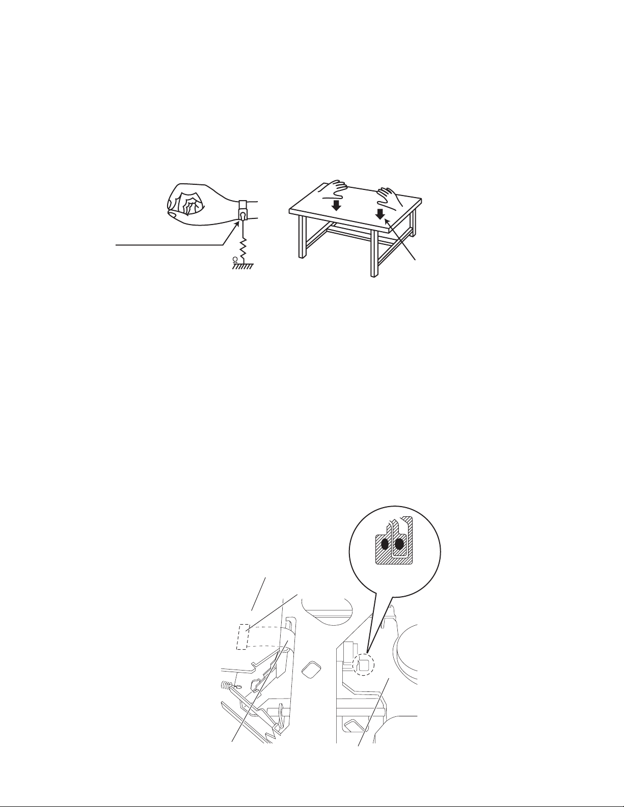
1.2 Preventing static electricity
Electrostatic discharge (ESD), which occurs when static electricity stored in the body, fabric, etc. is discharged, can destroy the laser
diode in the traverse unit (optical pickup). Take care to prevent this when performing repairs.
1.2.1 Grounding to prevent damage by static electricity
Static electricity in the work area can destroy the optical pickup (laser diode) in devices such as laser products.
Be careful to use proper grounding in the area where repairs are being performed.
(1) Ground the workbench
Ground the workbench by laying conductive material (such as a conductive sheet) or an iron plate over it before placing the
traverse unit (optical pickup) on it.
(2) Ground yourself
Use an anti-static wrist strap to release any static electricity built up in your body.
(caption)
Anti-static wrist strap
1M
Conductive material
(conductive sheet) or iron plate
(3) Handling the optical pickup
• In order to maintain quality during transport and before installation, both sides of the laser diode on the replacement optical
pickup are shorted. After replacement, return the shorted parts to their original condition.
(Refer to the text.)
• Do not use a tester to check the condition of the laser diode in the optical pickup. The tester's internal power source can easily
destroy the laser diode.
1.3 Handling the traverse unit (optical pickup)
(1) Do not subject the traverse unit (optical pickup) to strong shocks, as it is a sensitive, complex unit.
(2) Cut off the shorted part of the flexible cable using nippers, etc. after replacing the optical pickup. For specific details, refer to the
replacement procedure in the text. Remove the anti-static pin when replacing the traverse unit. Be careful not to take too long a
time when attaching it to the connector.
(3) Handle the flexible cable carefully as it may break when subjected to strong force.
(4) It is not possible to adjust the semi-fixed resistor that adjusts the laser power. Do not turn it.
1.4 Attention when traverse unit is decomposed
*Please refer to "Disassembly method" in the text for the pickup unit.
• Apply solder to the short land before the card wire is disconnected from the connector on the pickup unit.
(If the card wire is disconnected without applying solder, the pickup may be destroyed by static electricity.)
• In the assembly, be sure to remove solder from the short land after connecting the card wire.
Mechanism control board
CN102
Flexible wire
Short land section
Pickup
(No.MA429<Rev.002>)1-5
Page 6
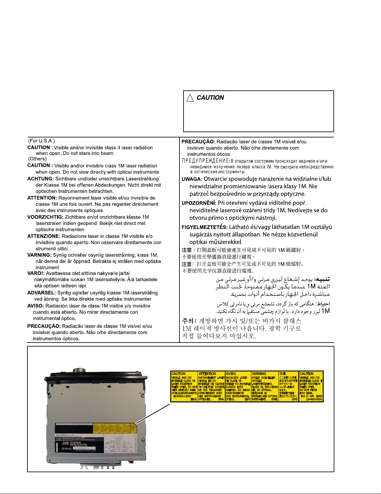
1.5 Important for laser products
1.CLASS 1 LASER PRODUCT
2.CAUTION :
(For U.S.A.) Visible and/or invisible class II laser radiation
when open. Do not stare into beam.
(Others) Visible and/or invisible class 1M laser radiation
when open. Do not view directly with optical instruments.
3.CAUTION : Visible and/or invisible laser radiation when
open and inter lock failed or defeated. Avoid direct
exposure to beam.
4.CAUTION : This laser product uses visible and/or invisible
laser radiation and is equipped with safety switches which
prevent emission of radiation when the drawer is open and
the safety interlocks have failed or are defeated. It is
dangerous to defeat the safety switches.
5.CAUTION : If safety switches malfunction, the laser is able
to function.
6.CAUTION : Use of controls, adjustments or performance of
procedures other than those specified here in may result in
hazardous radiation exposure.
!
Please use enough caution not to
see the beam directly or touch it
in case of an adjustment or operation
check.
REPRODUCTION AND POSITION OF LABELS and PRINT
WARNING LABEL and PRINT
1-6 (No.MA429<Rev.002>)
Page 7
SECTION 2
SPECIFIC SERVICE INSTRUCTIONS
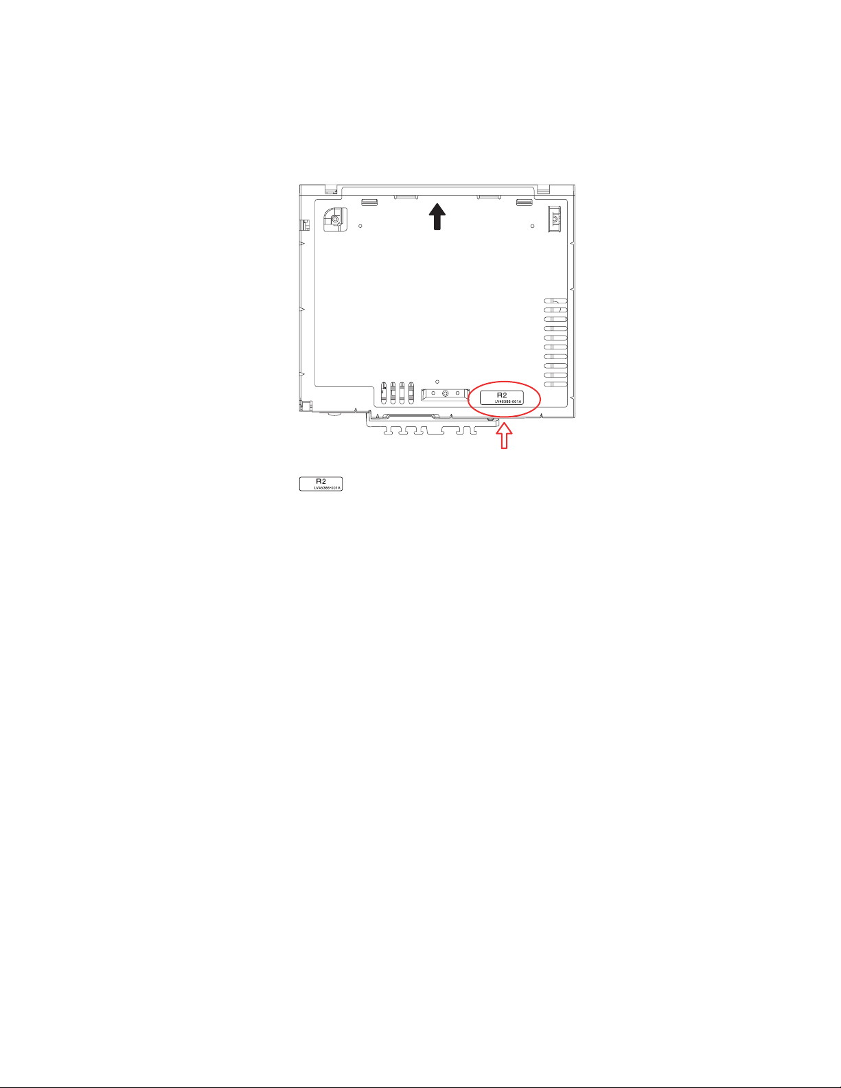
2.1 Identification method
Supported reduction in cost, and board contents was changed.
A set put the following label on is an object.
Front side
Top view
Label position
Change pwb parts
(No.MA429<Rev.002>)1-7
Page 8
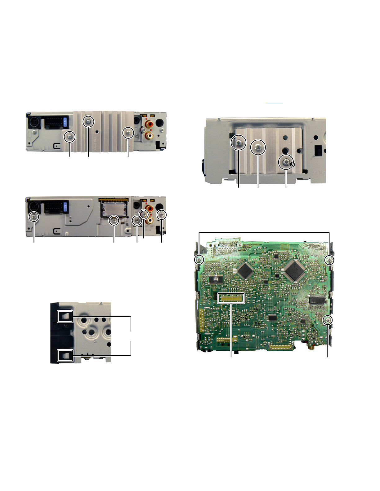
SECTION 3
DISASSEMBLY
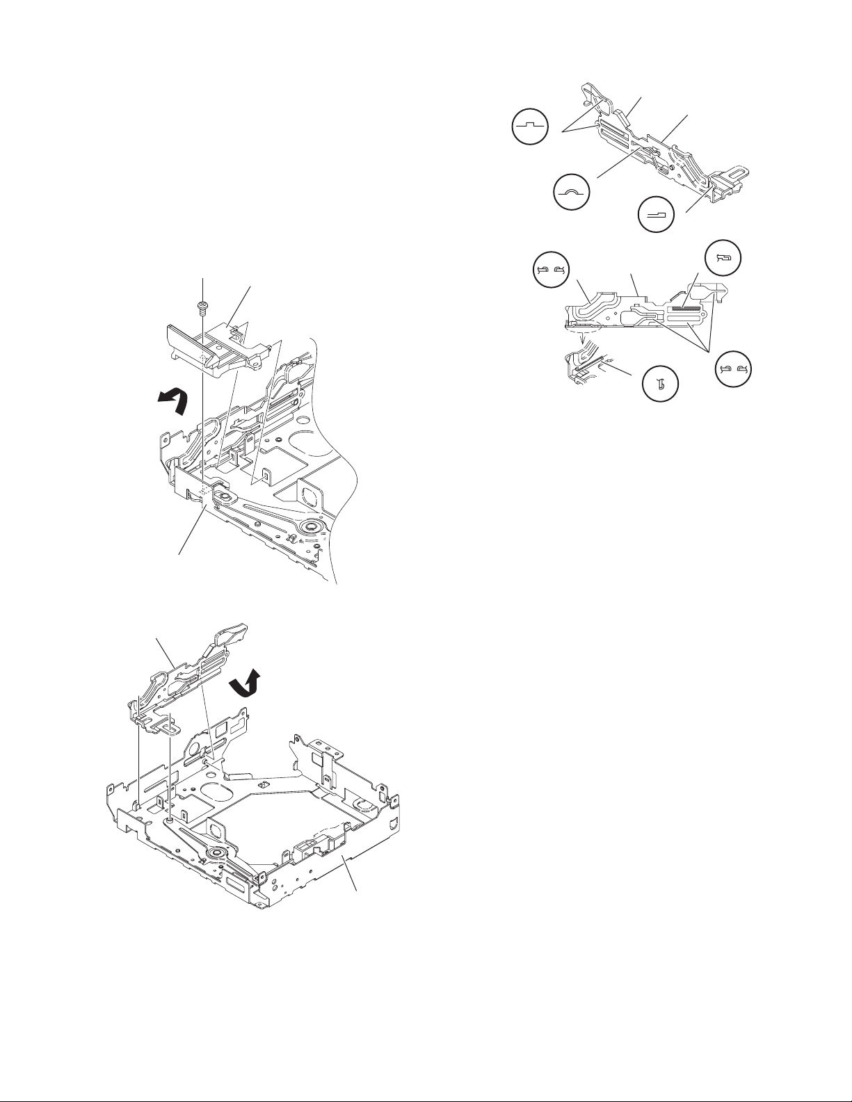
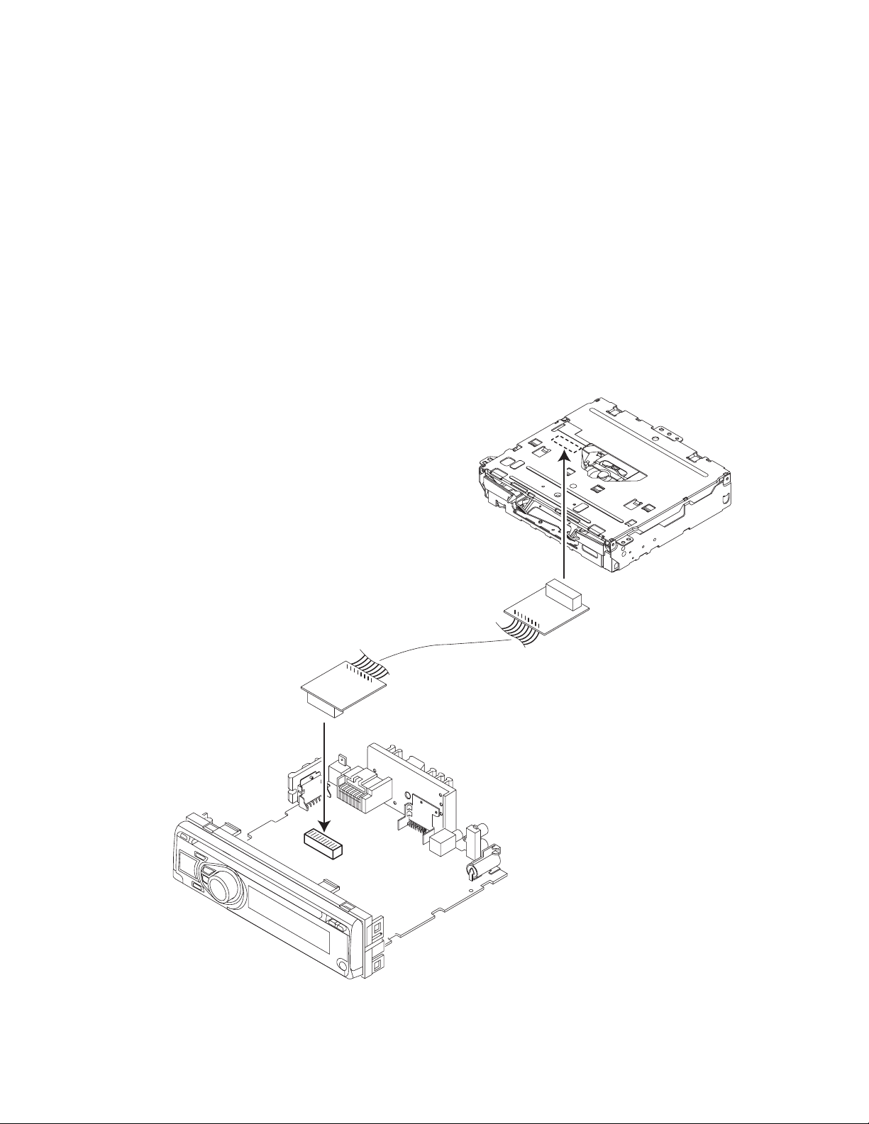
3.1 Main body (Used figure are KD-A305)
3.1.1 Removing the Bottom chassis (See Fig.1, 2)
(1) Remove the two screws A and one screw B attaching the
Heat sink. (See Fig.1)
(2) Remove the two screws C, two screws D and one screw E
attaching the Bottom chassis and then slide to backward
the Bottom chassis. (Se Fig.2)
AA B
Fig.1
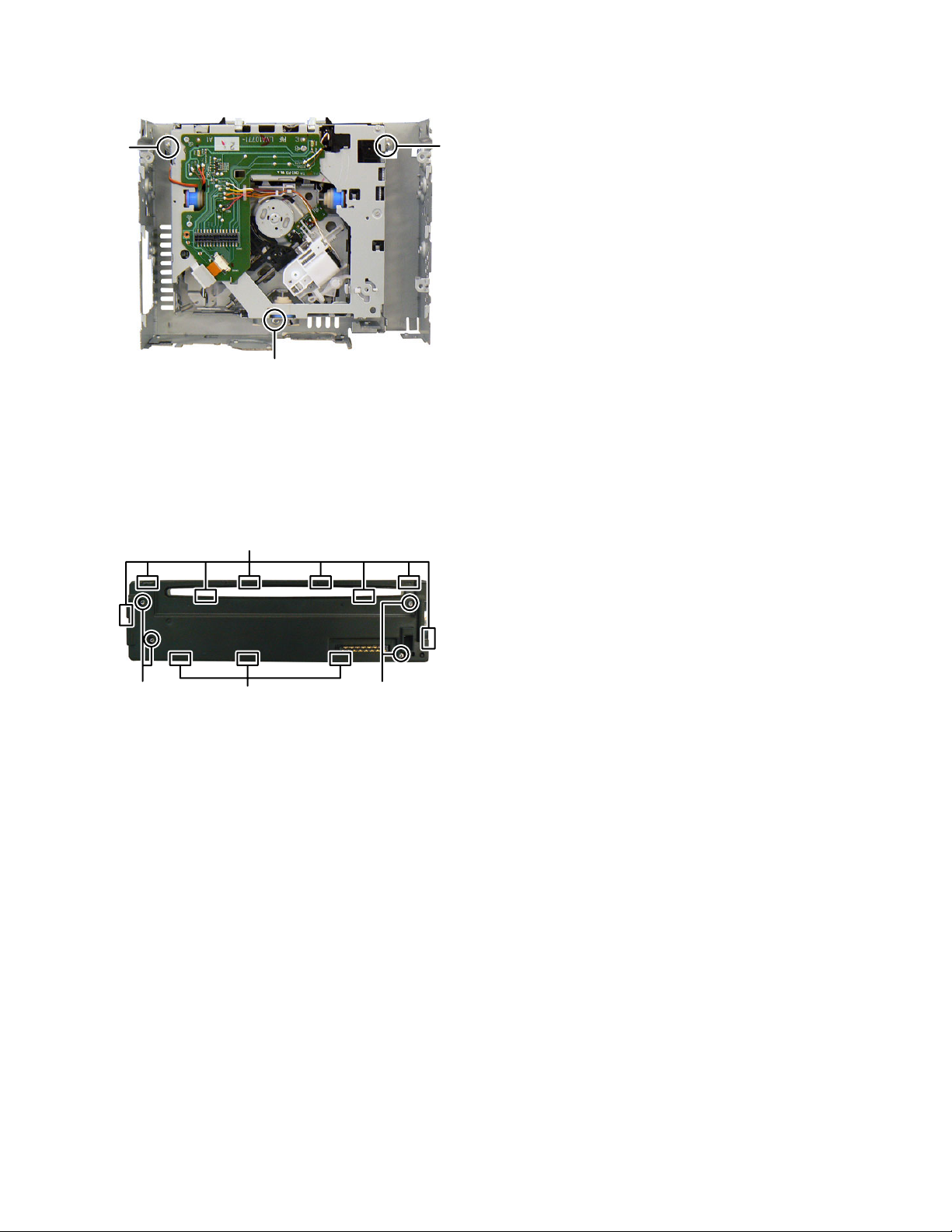
3.1.3 Removing the Main board (See Fig.4, 5)
(1) Remove the two screws F and one screw G attaching the
side plate. (See Fig.4)
(2) Remove the three screws H attaching the Main board. (See
Fig.5)
(3) Disconnect the connector CN501
CD mechanism. (See Fig.5)
of the main board from
FFG
Fig.4
hook
E
a
CCDD
Fig.2
3.1.2 Removing the Front chassis (See Fig.3)
(1) Disengage four hooks a engaged both side of the Front
chassis.
Fig.3
CN501
H
H
Fig.5
1-8 (No.MA429<Rev.002>)
Page 9
3.1.4 Removing the CD mechanism (See Fig.6)
(1) Remove the three screws J attaching the CD mechanism.
JJ
J
Fig.6
3.1.5 Removing the Switch board (See Fig.7)
(1) Remove the Volume knob.
(2) Remove the four screws K attaching the Rear cover.
(3) Disengage eleven hooks b engaged Rear cover.
hook
b
KK
hook
b
Fig.7
(No.MA429<Rev.002>)1-9
Page 10
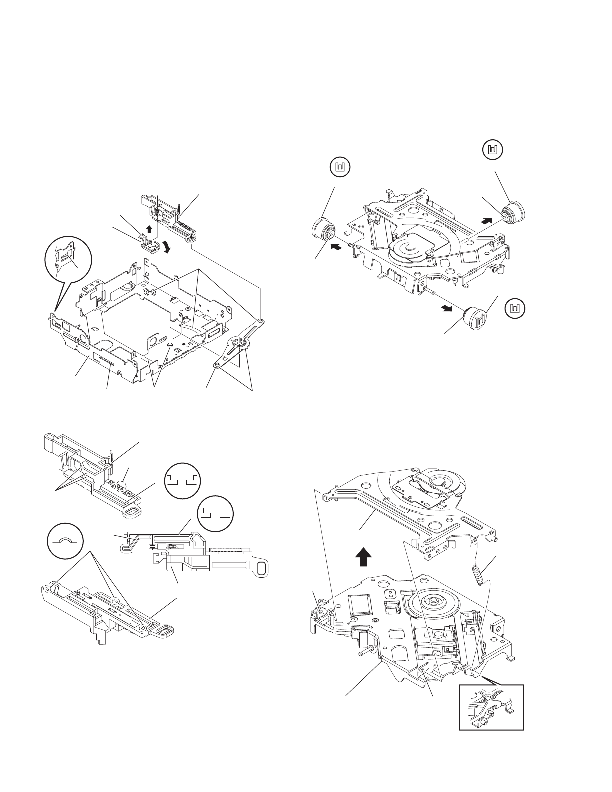
3.1.6 CD MECHANISM assembly section
• Remove the CD MECHANISM assembly from the main body.
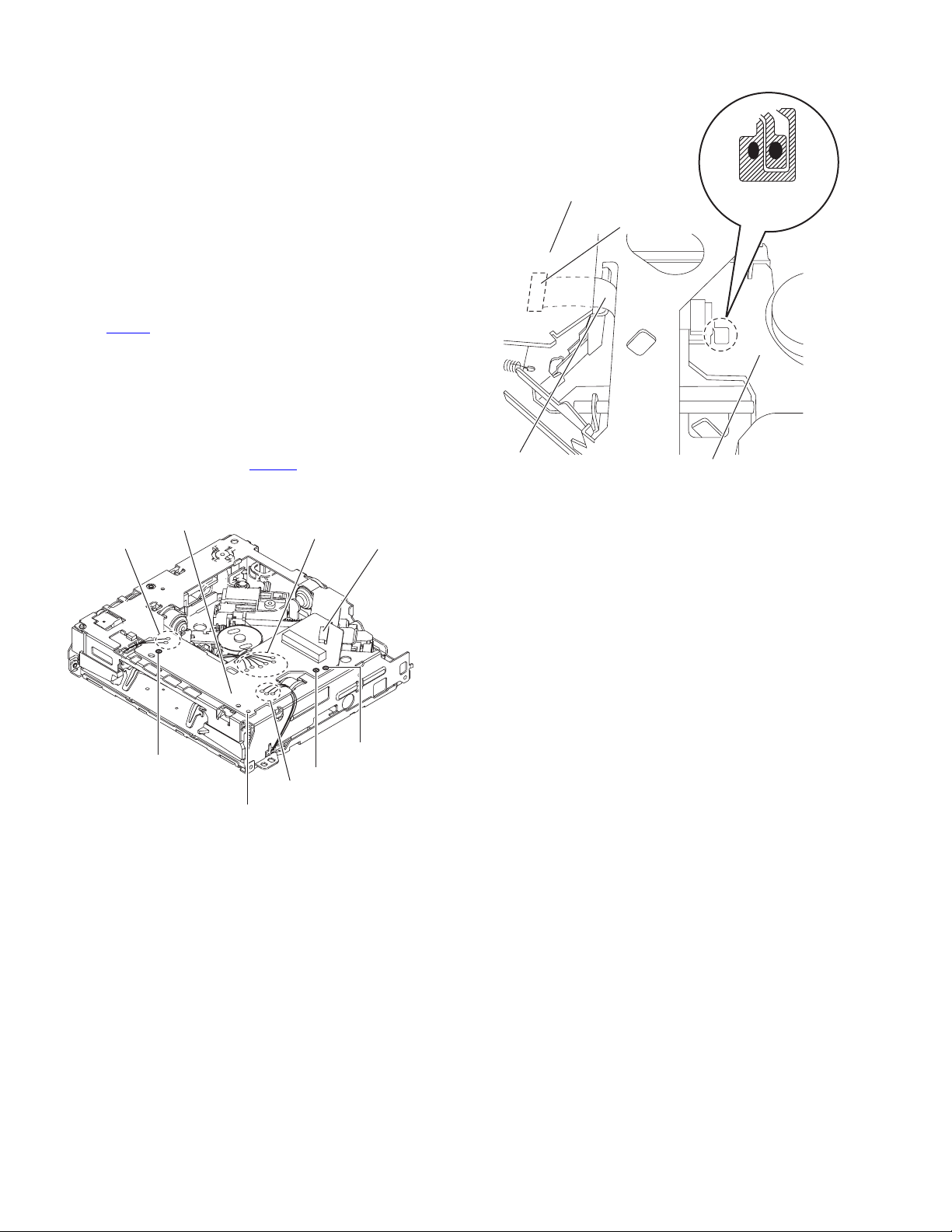
Removing the MECHANISM CONTROL BOARD
3.1.7
assembly (See Fig.
(1)
From the bottom side of CD MECHANISM assembly,
remove the solders from the soldered sections (
c
) on the MECHANISM CONTROL BOARD assembly.
1
(See Fig.
(2) Remove the three screws A and one screw B attaching the
MECHANISM CONTROL BOARD assembly. (See Fig.1.)
(3) Solder the short land sections on the pickup. (See Fig.2.)
Caution:
• Solder the short land sections on the pickup before
•
.)
disconnecting the flexible wire from the connector
on the MECHANISM CONTROL BOARD as-
CN102
sembly.
If the card wire is disconnected without attaching
solder, the pickup may be destroyed by static
electricity. (See Fig.
When attaching the MECHANISM CONTROL
BOARD assembly, remove the solders from the
short land sections after connecting the flexible
wire to the connector CN102
CONTROL BOARD assembly.
Mechanism
control board
a
1
and 2)
2
.)
a, b
and
on the MECHANISM
b
CN102
Mechanism control board
CN102
Flexible wire
Short land section
Pickup
Fig.2
A
1-10 (No.MA429<Rev.002>)
A
Fig.1
B
A
c
Page 11
3.1.8 Removing the top cover (See Fig.3 to 5)
• Remove the MECHANISM CONTROL BOARD assembly.
(1) From the front side of the CD MECHANISM assembly,
change the hook position of the two roller springs. (See
Fig.3.)
(2) From the side of the CD MECHANISM assembly, remove
the six screws C attaching the top cover. (See Fig.3 and 4.)
(3) Take out the top cover in an upward direction. (See Fig.5.)
Top cover
C
Roller spring Roller spring
Fig.3
Top cover
Fig.5
3.1.9 Removing the roller (See Fig.6)
• Remove the MECHANISM CONTROL BOARD assembly and
top cover.
(1) From the bottom side of the top cover, remove the screw D
attaching the gear holder.
(2) Remove the R.holder assembly from disc plate, and then
take out the roller from R.holder assembly in the direction
of the arrow.
Reference:
When attaching the R.ACT gear (2) and R.ACT gear (3),
apply grease to the section d of R.holder assembly.
Top cover
C
Fig.4
C
Gear holder
Roller gear
R.ACT gear(3)
R.ACT gear(2)
Top cover
D
d
R.holder assembly
Fig.6
Roller coller
Washer
Roller
Disc plate
(No.MA429<Rev.002>)1-11
Page 12
3.1.10 Removing the PHOTO BOARD assembly (See Fig.7 and 8)
• Remove the MECHANISM CONTROL BOARD assembly and
top cover.
(1)
From the bottom side of the top cover, release the
e
projection
Fig.
7
.)
(2) Take out the disc plate in the direction of the arrow. (See
Fig.7.)
(3) From the reverse side of the disc plate, remove the screw
E attaching the PHOTO BOARD assembly. (See Fig.8.)
from the notch of the disc plate. (See
e
e
SUS
spring
Mechanism section
Mecha frame
SUS
spring
F
Top cover
Fig.7
Disc plate
E
Photo board
Disc plate
Fig.8
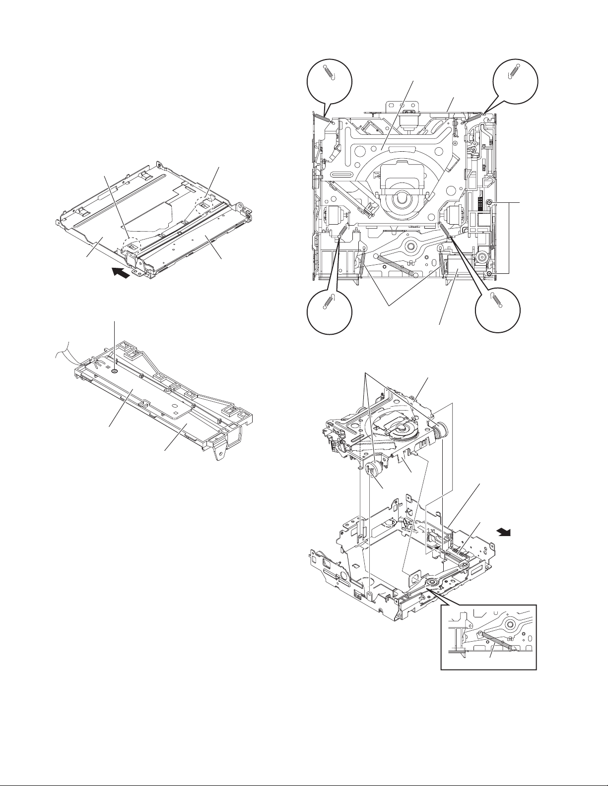
3.1.11 Removing the mechanism section (See Fig.9 and 10)
• Remove the MECHANISM CONTROL BOARD assembly and
top cover.
From the top side of the CD MECHANISM assembly,
(1)
F
remove the two screws
assembly. (See Fig.
(2) Remove the two roller springs on the top side of the mecha
frame. (See Fig.9.)
(3) Remove the four SUS springs on the top side of the mecha
frame. (See Fig.9.)
(4) Remove the link spring on the top side of the mecha frame.
(See Fig.10.)
(5) Release section f of the three dampers from the mecha
frame. (See Fig.10.)
Reference:
When attaching the roller spring and SUS spring, keep
direction before remove.
Move the slide cam (R) assembly in the direction of the
(6)
arrow, and then take out the mechanism section in an
upward direction. (See Fig.10.)
Reference:
When attaching the mechanism section, apply grease to
the section g. (See Fig.10.)
attaching the loading motor
9
.)
SUS
spring
Roller spring
Loading motor assembly
Fig.9
Damper
Mechanism section
g
f
Fig.10
SUS
spring
Mecha frame
Slidecam(R)
assembly
Link spring
1-12 (No.MA429<Rev.002>)
Page 13
3.1.12 Removing the slide cam (L) (See Fig.11 to 13)
• Remove the MECHANISM CONTROL BOARD assembly, top
cover and mechanism section.
(1) From the top side of the mecha frame, remove the screw G
attaching the cam cover. (See Fig.11.)
Take out the cam cover from mecha frame in an upward
(2)
11
direction. (See Fig.
(3) Take out the slide cam (L) in the direction of the arrow.
(See Fig.12.)
Reference:
When attaching the slide cam (L), apply grease to the
section h. (See Fig.13.)
.)
h
Slide cam(L)
h
h
h
Mecha frame
Slide cam(L)
G
Cam cover
Fig.11
h
Slide cam(L)
h
Fig.13
h
h
Fig.12
Mecha frame
(No.MA429<Rev.002>)1-13
Page 14
3.1.13 Removing the F.lock lever and slide cam (R) (See
Fig.14 and 15)
• Remove the MECHANISM CONTROL BOARD assembly, top
cover and mechanism section.
(1) From the top side of the mecha frame, take out the slide
cam (R) assembly in an upward direction. (See Fig.14.)
(2) Rotate the F.lock lever in the direction of the arrow 1, and
then take out the direction of the arrow 2. (See Fig.14.)
Reference:
When attaching the slide cam (R) assembly, the f.lock
lever and the link arm apply grease to the section
14
(See Fig.
and 15.)
h
Slide cam(R) assembly
h
F.lock lever
2
1
h
h
3.1.14 Removing the damper (See Fig.16)
• Remove the MECHANISM CONTROL BOARD assembly, top
cover and mechanism section.
From the mechanism section, pull out the three dampers in the
direction of the arrow.
Reference:
Before inserting the shaft to the dampers, apply IPA to the
pocket j of damper.
.
Damper (Gray)
Damper (Brown)
j
j
Damper (Brown)
j
Fig.16
Mecha frame
h
h
h
h
Fig.14
Link arm
Slide cam(R) assembly
h
h
h
Slide cam(R) assembly
Fig.15
3.1.15 Removing the clamper assembly (See Fig.17)
• Remove the MECHANISM CONTROL BOARD assembly, top
h
cover and mechanism section.
(1) From the top side of the mechanism section, release the
clamper spring.
(2) Move the clamper assembly in the direction of the arrow,
and then release the joints (k and m).
Take out the clamper assembly from the T.M chassis
(3)
assembly.
h
Clamper assembly
Clamper spring
k
1-14 (No.MA429<Rev.002>)
T.M. chassis assembly
m
Fig.17
Page 15
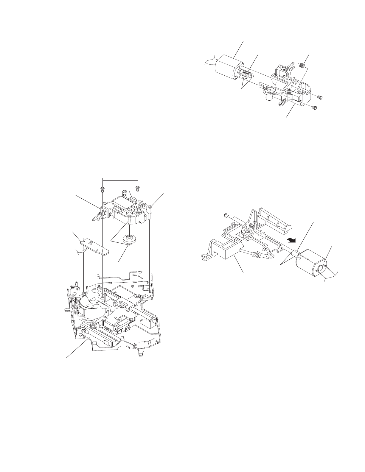
3.1.16 Removing the feed motor (See Fig.18 and 19)
r
• Remove the MECHANISM CONTROL BOARD assembly, top
cover, mechanism section and clamper assembly.
(1) From the bottom side of the T.M chassis assembly, remove
the two screws H attaching the feed motor assembly. (See
Fig.18.)
Remove the two screws J attaching the feed motor to
(2)
19
f.motor holder. (See Fig.
Reference:
When attaching the f. wheel gear, trigger arm and feed
motor, apply grease to the sections (n, p and q). (See
Fig.18 and 19.)
.)
Feed motor
F.worm gear
q
Comp. spring
J
3.1.17 Removing the SWITCH BOARD assembly (See
Fig.18)
• Remove the MECHANISM CONTROL BOARD assembly, top
cover, mechanism section, clamper assembly and feed motor
assembly.
From the bottom side of the T.M chassis assembly, take out
the SWITCH BOARD assembly in an upward direction from
T.M chassis assembly.
H
Feed motor assembly
Switch board
p
n
F.wheel gear
Trigger arm
F.motor holder
Fig.19
3.1.18 Removing the loading motor (See Fig.20)
• Remove the MECHANISM CONTROL BOARD assembly, top
cover, mechanism section and clamper assembly.
(1) From the right side of the L.M base assembly, remove the
two screws K attaching the loading motor.
(2) Take out the loading motor in the direction of the arrow
from the L.M base assembly.
Reference:
When attaching the loading motor, apply grease to the
section r.
K
r
L.M. base assembly
Fig.20
L.worm gear
Loading moto
T.M. chassis assembly
Fig.18
(No.MA429<Rev.002>)1-15
Page 16
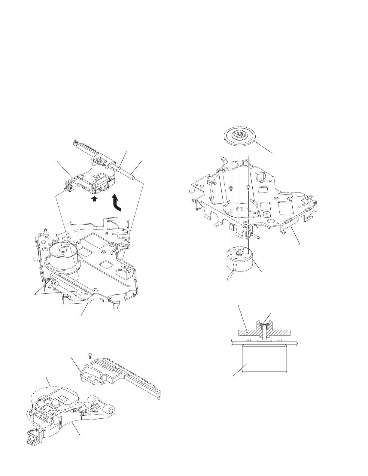
3.1.19 Removing the pickup assembly (See Fig.21 to 22)
• Remove the MECHANISM CONTROL BOARD assembly, top
cover, mechanism section, clamper assembly and feed motor
assembly.
Caution:
• Do not touch section u on the pickup assembly. (See Fig.21
and 22.)
(1) From the bottom side of the T.M chassis assembly, move
the pickup assembly in the direction of the arrow from the
T.M chassis assembly. (See Fig.21.)
(2) Pull out the main shaft. (See Fig.21.)
(3) Remove the screw M attaching the pickup to the rack plate.
(See Fig.22.)
Reference:
When attaching the loading motor, apply grease to the
sections s and t. (See Fig.21.)
3.1.20 Removing the spindle motor (See Fig.23 and 24)
Remove the MECHANISM CONTROL BOARD assembly,
•
top cover, mechanism section, clamper assembly, feed motor
assembly and pickup assembly.
(1) From the top side of the T.M chassis assembly, remove the
CD T.table assembly from the spindle motor. (See Fig.23.)
(2) Remove the two screws N attaching the spindle motor.
(See Fig.23.)
(3) Take out the spindle motor from the bottom side of the T.M
chassis assembly. (See Fig.23.)
Reference:
When attaching the CD T.table assembly to the spindle
motor shaft, apply loctite 460 to inside the CD T.table
assembly. (See Fig.24.)
Pick up assembly
s
T.M. chassis assembly
u
Fig.21
t
Main shaft
NN
Spindle motor
Fig.23
CD T.table assembly
CD T.table assembly
T.M.chassis assembly
Loctite
Rack plate
u
Pick up
1-16 (No.MA429<Rev.002>)
M
Spindle motor
Fig.24
Fig.22
Page 17
SECTION 4
ADJUSTMENT
4.1 Adjustment
Test instruments required for adjustment
(1) Digital oscilloscope (100MHz)
(2) Digital tester
(3) Test Disc
(4) Extension cable : EXTGS004-26PL
Standard volume position
Balance and Bass &Treble volume : lndication "0"
Loudness : OFF
How to connect the extension cable for adjusting
Be sure to attach the het sink and rear bracket onto the power amplifier IC and regulator IC respectively,
before supply the power.
If voltage is applied without attaching these parts, the power amplifier IC and regulator IC will be destroyed by heat.
Standard measuring conditions
Power supply voltage DC 14.4V(10.5 to 16V)
Load impedance 20K ohm (2 Speakers connection)
Dummy load
Exclusive dummy load should be used for AM, and FM.
For FM dummy load, there isa loss of 6dB between SSG
output and antenna input.
The loss of 6dB need not be considered since direct
reading of figures are applied in this working standard.
Extension cable
EXTGS004-26PL
(No.MA429<Rev.002>)1-17
Page 18
4.2 SERVICE MODE
DELEPROM
CD ERROR
CLR ERR
RUNNING1
RUNNING2
SIRIUS RST
XM RST
HD RESET
Clear EEPROM data
Display the CD Error past record in EEPROM.
Clear CD Error history from EEPROM.
For use in running tests.
For use in running tests.
SIRIUS Soft Reset
It clears all contents of built-in RAM and EEPROM, and performs software reset.
* Active at the time of SIRIUS connection.
XM Soft Reset
It clears all contents of built-in RAM and EEPROM, and performs software reset.
* Active at the time of XM connection.
HD Soft Reset
It clears all contents of built-in RAM and EEPROM, and performs software reset.
* Active at the time of HD connection.
DAB RESET
BT RESET
CDCHERR
DELCHERR
DAB Soft Reset
It clears all contents of built-in RAM and EEPROM, and performs software reset.
* Active at the time of DAB connection.
BT Soft Reset
It clears all contents of built-in RAM and EEPROM, and performs software reset.
* Active at the time of BT connection.
Display the CH Error past record stored in EEPROM
* Active at the time of CD CHANGER/IPOD (JBUS) connection
Clear CH Error history from EEPROM
* Active at the time of CD CHANGER/IPOD (JBUS) connection
1-18 (No.MA429<Rev.002>)
Page 19
4.3 TUNER SERVICE MODE
A
Key operation (FM, AM and DAB mode)
Enter service mode: [SEL] [MENU] (3 sec)
Exit service mode: press [ENTER] (SEL) key.
Go to next item: press [DISP] key
Back to previous item: press [BACK] key
VER=#*** MICON version display
# indicates destination: J=USA, U=OTHERS (eg. ASIA), R=EUROPE, E=EASTERN EUROPE
*** indicates version No.
########
Tuner device and version identification display
Display :TOM V1 for TOMIC V1 tuner.
Display :TOM V2 for TOMIC V2 tuner.
Display :ATOM V2 for ATOMIC V2 tuner.
Display: ATOM V3 for ATOMIC V3 tuner.
TINJ= ##
SPI=####
PI =####
PTY=##
TP=#TA=*
MS=#DI=*
AF=####
LEV= ##H
U&W= ##H
Tuner injection indicator
"##" indicates current tuner injection.
FOR DAB ONLY
To link SID display that DAB receives and FM station (Search PI), the reception situation of D
displayed.
"####" indicates SID code.
FOR RDS ONLY
PI display of receiving station, "####" indicates PI code.
PTY display of receiving station (00~29), "##" indicates PTY code.
TP, TA display of receiving station
"#" indicates TP ON/OFF: 1=ON; 0=OFF;
"*" indicates TA ON/OFF: 1=ON; 0=OFF.
M/S, DI display of receiving station
"#" indicates M/S ON/OFF: 1=ON; 0=OFF;
"*" indicates DI ON/OFF: 1=ON; 0=OFF.
Display the contents of AF memory (by scrolling) "####" indicate AF frequencies.
Fieldstrength indicator.
Adjacent and Multipath noise level indicator.
IFC= ##H
IFBW= #
RFAGC=##
IFAGC=##
##**
########
#####
IF COUNTER result indicator.
FM IF filter bandwidth indicator.
FM RF AGC resulting attenuation.
FM IF AGC resulting attenuation.
CLOCK display of receiving station (Original DISP key operation)
FOR RDS ONLY
PS NAME display of receiving station (Original DISP key operation)
FREQUENCY display of receiving station (Original DISP key operation)
(No.MA429<Rev.002>)1-19
Page 20
4.4 ERROR CODE
4.4.1 Mechanical Error Detail Codes
Condition Details Error Code Detail Code
Disc Loading Error
(1) B1 Time Out After detecting SW1=L, it does not become SW2=L 09 0011
(2) B2 Time Out After detecting SW2=H, it does not become SW2=L 09 0012
(3) C1 Time Out After detecting SW2=L, it does not become SW2=H 09 0013
Eject Error
(1) B1 Time Out After detecting SW2=H, it does not become SW2=L 01 0021
(2) C2 Time Out After detecting SW2=L, it does not become SW2=H 01 0022
(3) B2 Time Out After detecting SW1=L, it does not become SW2=L
immediately after RESET and so on.
(4) D0 Panel Close Disc can not be ejected due to closed panel. 01 0024
Forced Eject Error
(1) E1 Error SW1=H, SW2=L detected from NO DISC 01 0041
(2) E2 Error Detected SW1=L after RESET and then detected SW1=H 01 0042
(3) E3 Error Detected SW1=H after RESET 01 0043
(4) E4 Error Detected SW1=H after SW1=L 01 0044
(5) E5 Error Detected SW1=H after SW2=H→L 01 0045
(6) E6 Error Time Out for Loading after RESET 01 0046
(7) E7 Error Detected SW1=H after SW2=H→L→H 01 0047
(8) E8 Error Eject Key input while the procedure is not completed after
Forced Eject execution
(9) Error Eject Key input during Disc is on the way and not completed 01 0049
Loading Waiting Error
(1) SW1=H or NO DISC
detection before Loading
Motor activation during
Disc is waiting at thewaiting location.
(2) SW2=L before Loading
Motor activation during
Disc is waiting at thewaiting location.
Disc is removed or NO DISC detection condition 09 0031
Disc is inserted 09 0032
01 0023
01 0048
4.4.2 CD changer mechanism error code
Error contents Details Error code Detail code
Tray eject error Tray motor time over
1.TRAYINSW time over
(TRAYINSW:LTRAYOUTSW:H)
2.TRAYOUTSW time over
(TRAYINSW:HTRAYOUTSW:H)
3.TRAYINSW time over
(TRAYINSW:LTRAYOUTSW:L)
4.MAGIN SW:L→H Magazine is ejected while Tray is being ejected. 03 0014
Tray return error Tray motor time over
1.TRAYOUTSW time over
(TRAYINSW:HTRAYOUTSW:L)
2.TRAYINSW time over
(TRAYINSW:HTRAYOUTSW:H)
3.TRAYIN/OUTSW time over
(TRAYINSW:LTRAYOUTSW:L)
4.MAGIN SW:L→H Magazine is ejected while Tray is being returned. 03 0019
1-20 (No.MA429<Rev.002>)
Tray motor does not operate. 03 0011
Tray stops. 03 0012
TRAYINSW NG etc. 03 0013
Tray motor does not operate. 03 0016
Tray stops. 03 0017
TRAYOUTSW NG etc. 03 0018
Page 21
Lifter up error Position motor time over
1.WAIT position time over Position motor does not operate. 02 0021
2.WAIT position time over Position is not stable in fine adjustment mode. 02 0022
3.WAIT position time over Other condition 02 0023
Lifter down error Position motor time over
1.WAIT position time over Position motor does not operate. 02 0026
2.WAIT position time over Position is not stable in fine adjustment mode. 02 0027
3.WAIT position time over Other condition 02 0028
Chucking error Position motor time over
1.Play position time over Position motor does not operate. 02 0031
2.Play position time over Position is not stable in fine adjustment mode. 02 0032
3.Play position time over Other condition 02 0033
Unchucking error Position motor time over
1.WAIT position time over Position motor does not operate. 02 0036
2.WAIT position time over Position is not stable in fine adjustment mode. 02 0037
3.WAIT position time over Other condition 02 0038
Eject error Eject cannot be carried out.
1.Eject position time over Position motor does not operate. 02 0041
2.Eject position time over Improper EJECT position.* 02 0042
3.MAGINSW time over Magazine is not ejected. 01 0043
Initialize error
1.Mechanism SW NG error TRAYINSW and TRAYOUTSW are L. 03 0046
2.Absolute position time over Position is not stable in absolute position.* 02 0047
*"Position is not stable in WAIT position," "Position is not stable in PLAY position," and "Position is not stable in
absolute position" and "Improper EJECT position" are all Position Motor TIME OVER.
4.4.3 CD changer disc error code
Error contents Details Error code Detail code
Pickup movement error Time over at PUBWD and PUFWD by monitoring RESET SW.
1.Time over of pickup movement
in an inner direction(10s)
2.Time over of pickup movement
in an outer direction(10s)
Focus search error
Focus is not adjusted by 3-round focus search
Tracking balance adjustment error
Time over(1s)
TOC area search error
Time over(10s)
Focus balance adjustment error
Time over(2s)
Focus gain adjustment error
Time over(0.6s)
TOC read error. Time over(30s) TOC read operation is not finished after 30s. 84 0059
First track access error
Time over(10s)
Last track access error
Time over(10s)
Q code read error
Time over(0.6s)
Pickup cannot move in an inner direction.
RESET SW is not on.
Pickup cannot move in an outer direction.
RESET SW is not off.
When focus is not adjusted by 3-round(1set)
focus search after disc change or focus shock the result is NG
Tracking balance adjustment is not finished 1s
after adjustment command(TBA) is executed.
TOC area search is not finished after 10s. 80 0055
Focus balance adjustment is not finished 2s
after adjustment command(FBA) is executed.
Focus gain adjustment error is not finished 0.6s
after adjustment command(FGA) is executed.
First track access is not finished 10s after TOC
reading is finished.
Last track access is not finished 10s after first track in running mode. 80 0061
Q code is not read for 0.6s during playback of
TOC and program area.
04 0051
04 0052
81 0053
82 0054
82 0056
82 0057
80 0060
80 0062
(No.MA429<Rev.002>)1-21
Page 22

SECTION 5
TROUBLESHOOTING
5.1 16 PIN CORD DIAGRAM (For KD-A305, KD-R300, KD-S26)
1
16
8
GN
7
GN/BK
6
VI/BK
5
VI
4
NC
BL/WH
3
RD
2
BK
1
BK
YL
RD
2
GN
8
WH
WH/BK
GY/BK
GY
NC
NC
NC
YL
9
10
11
12
13
14
15
16
BK
RD
BL
WH
Black
Red
Blue
White
VI
GN
GY
YL
Violet
Green
Gray
Yellow
7
5
6
9
10
12
11
3
GN/BK
VI
VI/BK
WH
WH/BK
GY
GY/BK
BL/WH
1-22 (No.MA429<Rev.002>)
Page 23

5.2 16 PIN CORD DIAGRAM (For KD-R404, KD-R405, KD-R406)
1
16
4
3
8
7
6
5
4
3
2
1
BK
YL
BL
BL/WH
GN
GN/BK
VI/BK
VI
BL
BL/WH
RD
BK
WH
WH/BK
GY/BK
GY
NC
NC
NC
YL
9
10
11
12
13
14
15
16
BK
RD
BL
WH
Black
Red
Blue
White
VI
GN
GY
YL
Violet
Green
Gray
Yellow
2
8
7
5
6
9
10
12
11
RD
GN
GN/BK
VI
VI/BK
WH
WH/BK
GY
GY/BK
(No.MA429<Rev.002>)1-23
Page 24

Victor Company of Japan, Limited
Mobile Entertainment Division 10-1,1chome,Ohwatari-machi,Maebashi-city,371-8543,Japan
(No.MA429<Rev.002>)
Printed in Japan
VSE
Page 25

REVISION INFORMATION
CD RECEIVER
KD-A305J, KD-R300J, KD-R404UI,
KD-R405U, KD-R405UN, KD-R405UT,
KD-R405UH, KD-R406U, KD-R406UN,
KD-R406UT, KD-R406UH, KD-S26J
■ OVERVIEW
Add KD-S26J, supported reduction in cost, and board contents were changed.
■ DETAILS
COVER SECTION
Title Line No.MA429<Rev.001> No.MA429<Rev.002> Description
Revision Rev.001 Rev.002
Issue Date 2008/10 2009/08
Model No. KD-A305J, KD-R300J, KD-R404UI,
Cover Illustration ILLUSTRATION(ma429_0001.png) ILLUSTRATION(ma429_0001.png)
Copyright COPYRIGHT (C) 2008 Victor Company of
SPECIFICATION 1 KD-A305/KD-R300 KD-A305/KD-R300/KD-S26
11
13
KD-R405U, KD-R405UH, KD-R405UN,
KD-R405UT, KD-R406U, KD-R406UH,
KD-R406UN, KD-R406UT
Japan, Limited
KD-R300
2.5 V/20 kΩ load (full scale)
KD-R300
2.5 V/20 kΩ load (full scale)
SECTION 2 SPECIFIC SERVICE INSTRUCTIONS
Title Line No.MA429<Rev.001> No.MA429<Rev.002> Description
2 SPECIFIC SERVICE
INSTRUCTIONS
1 This service manual does not describe
SPECIFIC SERVICE INSTRUCTIONS.
KD-A305J, KD-R300J, KD-R404UI,
KD-R405U, KD-R405UH, KD-R405UN,
KD-R405UT, KD-R406U, KD-R406UH,
KD-R406UN, KD-R406UT, KD-S26J
COPYRIGHT (C) 2009 Victor Company of
Japan, Limited
KD-R300/KD-S26
2.5 V/20 kΩ load (full scale)
KD-R300/KD-S26
2.5 V/20 kΩ load (full scale)
-
COPYRIGHT © 2009 Victor Company of Japan, Limited
MA429-R002
2009/08
Page 26

Title Line No.MA429<Rev.001> No.MA429<Rev.002> Description
r
2.1 Identification method T - 2.1 Identification method
1 - Supported reduction in cost, and board contents was
changed.A set put the following label on is an object.
2 - ILLUSTRATION(ma429_2001.png)
SECTION 5 TROUBLESHOOTING
Title Line No.MA429<Rev.001> No.MA429<Rev.002> Description
5.1 16 PIN CORD DIAGRAM (For
KD-A305, KD-R300, KD-S26)
T 5.1 16 PIN CORD DIAGRAM (For KD-
A305, KD-R300)
5.1 16 PIN CORD DIAGRAM (For KDA305, KD-R300, KD-S26)
STANDARD SCHEMATIC DIAGRAMS
Schematic Diagram
Diagram Name No.MA429<Rev.001> No.MA429<Rev.002> Description
Menu Main section Old Main section
Menu CD section Old CD section
Menu LCD & Key control section Old LCD & Key control section
Menu - Main section
Menu - CD section
Menu - LCD & Key control section
Printed Circuit Board
Diagram Name No.MA429<Rev.001> No.MA429<Rev.002> Description
Menu Main board Old Main board
Menu Switch board Old Switch board
Menu LED board Old LED board
Menu - Main board
Menu - Switch board
Menu - LED board
Description of Major ICs
Diagram Name No.MA429<Rev.001> No.MA429<Rev.002> Description
Menu - IC681: KSM-2003TN2M
Menu IC701: MN101E16YFA IC701: MN101E16YFA1
Menu IC1: TEF6606T/V3-X IC1: TEF6606T/V5-X
PARTS LIST
MODEL No. LIST
Model No. No.MA429<Rev.002>
KD-A305J 01
KD-R300J 02
KD-R404UI 03
KD-R405U 04
General assembly [M1MM]
Symbol o
!
M1MM 2 ------------ GE33323-001A HEAT SINK (Addition) 1 0C
M1MM 2 GE33323-001A GE33323-002A HEAT SINK 1 01,02,03,04,05,06,07,08,09,0A,0B
M1MM 4 ------------ GE33325-003A INSULATOR (Addition) 1 0C
M1MM 15 ------------ GE10242-008A FRONT CHASSIS (Addition) 1 0C
M1MM 15 GE10242-001A GE10242-005A FRONT CHASSIS 1 01,02,03,04,05,06,07,08,09,0A,0B
M1MM 21 GE10243-006A GE10243-011A FRONT PANEL 1 01
M1MM 21 GE10243-005A GE10243-010A FRONT PANEL 1 02,0C
<Rev.001> <Rev.002>
2 (MA429-R002)
Part No.
Model No. No.MA429<Rev.002>
KD-R405UH 07
KD-R405UN 05
KD-R405UT 06
KD-R406U 08
Part Name Description Qty Models
Model No. No.MA429<Rev.002>
KD-R406UH 0B
KD-R406UN 09
KD-R406UT 0A
KD-S26J 0C
Page 27

Symbol o
r
r
!
M1MM 21 GE10243-007A GE10243-012A FRONT PANEL 1 03,04,05,06,07
M1MM 21 GE10243-008A GE10243-013A FRONT PANEL 1 08,09,0A,0B
M1MM 22 ------------ GE33342-038A FINDER ASSY (Addition) 1 0C
M1MM 31 GE33312-004A GE33312-006A NAVI BTN HI 1 01,02,08,09,0A,0B,0C
M1MM 31 GE33312-003A GE33312-005A NAVI BTN HI 1 03,04,05,06,07
M1MM 35 ------------ GE10244-003A REAR COVER (Addition) 1 0C
M1MM 40 GE40440-001A GE40440-003A LIGHTING SHEET 1 01,02,03,04,05,06,07,08,09,0A,0B,0C
M1MM 41 ------------ GE33872-001A NAME PLATE (Addition) 1 0C
M1MM 49 GE31574-104A GE31574-0A5A UT LABEL 1 0A
M1MM 53 ------------ LV45386-001A R2 INDICATION (Addition) 1 01,02,03,04,05,06,07,08,09,0A,0B
M1MM 54 ------------ GE40225-001A CAR STEREO TAG (Addition) 1 0C
M1MM 55 ------------ QYSDSP4014ZA SCREW (Addition) 1 0C
M1MM 56 ------------ GE40282-001A LABEL (Addition) 1 0C
<Rev.001> <Rev.002>
Part No.
Part Name Description Qty Models
CD mechanism FLM-CD2-1D [MBMM]
Symbol o
!
MBMM 2 LV36800-001A LV36800-002A LINK ARM 1 01,02,03,04,05,06,07,08,09,0A,0B,0C
MBMM 30 LV44640-001A LV45227-001A RACK SPRING 1 01,02,03,04,05,06,07,08,09,0A,0B,0C
MBMM 51 LV36801-001A LV36801-002A GEAR HOLDER 1 01,02,03,04,05,06,07,08,09,0A,0B,0C
MBMM 57 LV22325-001A LV22325-002A R HOLDER ASSY 1 01,02,03,04,05,06,07,08,09,0A,0B,0C
<Rev.001> <Rev.002>
Part No.
Part Name Description Qty Models
Mecha control board FLM-CD2-1D [03]
Symbol or
!
03 Q101 or ------------ 2SD601A/R/-X TRANSISTOR (Addition) 1 01,02,03,04,05,06,07,08,09,0A,0B,0C
03 Q201 or ------------ 2SD601A/R/-X TRANSISTOR (Addition) 1 01,02,03,04,05,06,07,08,09,0A,0B,0C
<Rev.001> <Rev.002>
Part No.
Part Name Description Qty Models
Main board [04]
Symbol or
!
! 04 IC1 ------------ TEF6606T/V5-X IC (Addition) 1 01,02,03,04,05,06,07,08,09,0A,0B,0C
04 IC161 ------------ BD3700FV-X IC (Addition) 1 01,02,03,04,05,06,07,08,09,0A,0B,0C
! 04 IC301 ------------ TB2926CHQ IC (Addition) 1 01,02,03,04,05,06,07,08,09,0A,0B,0C
04 IC381 ------------ NJM2160BV-X IC (Addition) 1 01
! 04 IC501 ------------ LA6565-X IC (Addition) 1 01,02,03,04,05,06,07,08,09,0A,0B,0C
! 04 IC521 ------------ MN6627945EE IC (Addition) 1 01,02,03,04,05,06,07,08,09,0A,0B,0C
04 IC581 ------------ NJM4565E-X IC (Addition) 1 01,02,03,04,05,06,07,08,09,0A,0B,0C
! 04 IC701 ------------ MN101E16YFA1 IC (Addition) 1 01,02,03,04,05,06,07,08,09,0A,0B,0C
04 IC702 ------------ S-80824CNNB-G-W IC (Addition) 1 01,02,03,04,05,06,07,08,09,0A,0B,0C
04 IC702 or ------------ IC-PST3424U-X IC (Addition) 1 01,02,03,04,05,06,07,08,09,0A,0B,0C
04 IC801 ------------ 74AHCT126PW-X IC (Addition) 1 01,02,03,04,05,06,07,08,09,0A,0B,0C
! 04 IC901 ------------ AN34001A IC (Addition) 1 01,02,03,04,05,06,07,08,09,0A,0B,0C
04 IC981 ------------ NJM2878F4-15-X IC (Addition) 1 01,02,03,04,05,06,07,08,09,0A,0B,0C
04 Q341 ------------ IMX9-W PAIR
04 Q501 ------------ 2SA1705/ST/-T TRANSISTOR (Addition) 1 01,02,03,04,05,06,07,08,09,0A,0B,0C
04 Q521 ------------ ISA1530AC1/R/-X TRANSISTOR (Addition) 1 01,02,03,04,05,06,07,08,09,0A,0B,0C
04 Q521 or ------------ 2SA2077-X TRANSISTOR (Addition) 1 01,02,03,04,05,06,07,08,09,0A,0B,0C
04 Q781 ------------ RT1P141C-X DIGI
04 Q781 or ------------ UN2111-X TRANSISTOR (Addition) 1 01,02,03,04,05,06,07,08,09,0A,0B,0C
04 Q782 ------------ 2SC3928A/QR/-X TRANSISTOR (Addition) 1 01,02,03,04,05,06,07,08,09,0A,0B,0C
04 Q782 or ------------ 2SC5845-X TRANSISTOR (Addition) 1 01,02,03,04,05,06,07,08,09,0A,0B,0C
04 Q784 ------------ RT1P141C-X DIGI
04 Q784 or ------------ UN2111-X TRANSISTOR (Addition) 1 01,02,03,04,05,06,07,08,09,0A,0B,0C
04 Q785 ------------ RT1P141C-X DIGI
04 Q785 or ------------ UN2111-X TRANSISTOR (Addition) 1 01,02,03,04,05,06,07,08,09,0A,0B,0C
04 Q921 ------------ 2SB1132/QR/-W TRANSISTOR (Addition) 1 03,04,05,06,07,08,09,0A,0B
04 Q922 ------------ RT1N141C-X DIGI
04 Q922 or ------------ UN2211-X TRANSISTOR (Addition) 1 03,04,05,06,07,08,09,0A,0B
04 Q976 ------------ RT1N141C-X DIGI
04 Q976 or ------------ UN2211-X TRANSISTOR (Addition) 1 01,02,03,04,05,06,07,08,09,0A,0B,0C
04 Q977 ------------ ISA1530AC1/R/-X TRANSISTOR (Addition) 1 01,02,03,04,05,06,07,08,09,0A,0B,0C
<Rev.001> <Rev.002>
Part No.
Part Name Description Qty Models
(Addition) 1 01,02,03,04,05,06,07,08,09,0A,0B,0C
TRANSISTOR
(Addition) 1 01,02,03,04,05,06,07,08,09,0A,0B,0C
TRANSISTOR
(Addition) 1 01,02,03,04,05,06,07,08,09,0A,0B,0C
TRANSISTOR
(Addition) 1 01,02,03,04,05,06,07,08,09,0A,0B,0C
TRANSISTOR
(Addition) 1 03,04,05,06,07,08,09,0A,0B
TRANSISTOR
(Addition) 1 01,02,03,04,05,06,07,08,09,0A,0B,0C
TRANSISTOR
(MA429-R002) 3
Page 28

Symbol or
!
04 Q977 or ------------ 2SA2077-X TRANSISTOR (Addition) 1 01,02,03,04,05,06,07,08,09,0A,0B,0C
04 D331 ------------ MC2836-X DIODE (Addition) 1 01,02,03,04,05,06,07,08,09,0A,0B,0C
04 D331 or ------------ MA152WA-X DIODE (Addition) 1 01,02,03,04,05,06,07,08,09,0A,0B,0C
04 D501 ------------ 1A3G-T1 SI DIODE (Addition) 1 01,02,03,04,05,06,07,08,09,0A,0B,0C
04 D711 ------------ MA8062/M/-X Z DIODE (Addition) 1 01
04 D711 or ------------ UDZW6.2B-X Z DIODE (Addition) 1 01
04 D712 ------------ MA111-X SI DIODE (Addition) 1 01,02,03,04,05,06,07,08,09,0A,0B,0C
04 D712 or ------------ 1SS355W-X DIODE (Addition) 1 01,02,03,04,05,06,07,08,09,0A,0B,0C
04 D715 ------------ MA8062/M/-X Z DIODE (Addition) 1 01,02,03,04,05,06,07,08,09,0A,0B,0C
04 D715 or ------------ UDZW6.2B-X Z DIODE (Addition) 1 01,02,03,04,05,06,07,08,09,0A,0B,0C
04 D716 ------------ MA8062/M/-X Z DIODE (Addition) 1 01,02,03,04,05,06,07,08,09,0A,0B,0C
04 D716 or ------------ UDZW6.2B-X Z DIODE (Addition) 1 01,02,03,04,05,06,07,08,09,0A,0B,0C
04 D717 ------------ MA8062/M/-X Z DIODE (Addition) 1 01,02,03,04,05,06,07,08,09,0A,0B,0C
04 D717 or ------------ UDZW6.2B-X Z DIODE (Addition) 1 01,02,03,04,05,06,07,08,09,0A,0B,0C
04 D718 ------------ MA8062/M/-X Z DIODE (Addition) 1 01,02,03,04,05,06,07,08,09,0A,0B,0C
04 D718 or ------------ UDZW6.2B-X Z DIODE (Addition) 1 01,02,03,04,05,06,07,08,09,0A,0B,0C
04 D781 ------------ MA111-X SI DIODE (Addition) 1 01,02,03,04,05,06,07,08,09,0A,0B,0C
04 D781 or ------------ 1SS355W-X DIODE (Addition) 1 01,02,03,04,05,06,07,08,09,0A,0B,0C
04 D782 ------------ MA111-X SI DIODE (Addition) 1 01,02,03,04,05,06,07,08,09,0A,0B,0C
04 D782 or ------------ 1SS355W-X DIODE (Addition) 1 01,02,03,04,05,06,07,08,09,0A,0B,0C
04 D784 ------------ MA8100/M/-X Z DIODE (Addition) 1 01,02,03,04,05,06,07,08,09,0A,0B,0C
04 D784 or ------------ UDZW10B-X Z DIODE (Addition) 1 01,02,03,04,05,06,07,08,09,0A,0B,0C
04 D786 ------------ MA111-X SI DIODE (Addition) 1 01,02,03,04,05,06,07,08,09,0A,0B,0C
04 D786 or ------------ 1SS355W-X DIODE (Addition) 1 01,02,03,04,05,06,07,08,09,0A,0B,0C
04 D787 ------------ MA111-X SI DIODE (Addition) 1 01,02,03,04,05,06,07,08,09,0A,0B,0C
04 D787 or ------------ 1SS355W-X DIODE (Addition) 1 01,02,03,04,05,06,07,08,09,0A,0B,0C
04 D851 ------------ MA22F20-X SB DIODE (Addition) 1 03,04,05,06,07,08,09,0A,0B
04 D852 ------------ MA22D39-X SB DIODE (Addition) 1 03,04,05,06,07,08,09,0A,0B
! 04 D901 ------------ 1N5401-F64 SI DIODE (Addition) 1 01,02,03,04,05,06,07,08,09,0A,0B,0C
! 04 D901 or ------------ 1N5401-TU-15 SI DIODE (Addition) 1 01,02,03,04,05,06,07,08,09,0A,0B,0C
04 D971 ------------ MA22F20-X SB DIODE (Addition) 1 01,02,03,04,05,06,07,08,09,0A,0B,0C
04 D972 ------------ MA22D39-X SB DIODE (Addition) 1 01,02,03,04,05,06,07,08,09,0A,0B,0C
04 C1 ------------ NCB31HK-102X C CAPACITOR (Addition) 1 01,02,03,04,05,06,07,08,09,0A,0B,0C
04 C2 ------------ NDC31HJ-7R0X C CAPACITOR (Addition) 1 01,02,03,04,05,06,07,08,09,0A,0B,0C
04 C3 ------------ NCB31HK-102X C CAPACITOR (Addition) 1 01,02,03,04,05,06,07,08,09,0A,0B,0C
04 C4 ------------ NCB31AK-224X C CAPACITOR (Addition) 1 01,02,03,04,05,06,07,08,09,0A,0B,0C
04 C5 ------------ NDC31HJ-150X C CAPACITOR (Addition) 1 01,02,03,04,05,06,07,08,09,0A,0B,0C
04 C6 ------------ NDC31HJ-2R0X C CAPACITOR (Addition) 1 01,02,03,04,05,06,07,08,09,0A,0B,0C
04 C7 ------------ NDC31HJ-220X C CAPACITOR (Addition) 1 01,02,03,04,05,06,07,08,09,0A,0B,0C
04 C10 ------------ NCB21AK-105X C CAPACITOR (Addition) 1 01,02,03,04,05,06,07,08,09,0A,0B,0C
04 C11 ------------ NCB31HK-103X C CAPACITOR (Addition) 1 01,02,03,04,05,06,07,08,09,0A,0B,0C
04 C12 ------------ NCB31HK-103X C CAPACITOR (Addition) 1 01,02,03,04,05,06,07,08,09,0A,0B,0C
04 C13 ------------ NCB21AK-105X C CAPACITOR (Addition) 1 01,02,03,04,05,06,07,08,09,0A,0B,0C
04 C14 ------------ NCB31AK-224X C CAPACITOR (Addition) 1 01,02,03,04,05,06,07,08,09,0A,0B,0C
04 C15 ------------ NCB31CK-104X C CAPACITOR (Addition) 1 01,02,03,04,05,06,07,08,09,0A,0B,0C
04 C16 ------------ NCB31HK-103X C CAPACITOR (Addition) 1 01,02,03,04,05,06,07,08,09,0A,0B,0C
04 C17 ------------ NCB31CK-104X C CAPACITOR (Addition) 1 01,02,03,04,05,06,07,08,09,0A,0B,0C
04 C18 ------------ NCB31HK-103X C CAPACITOR (Addition) 1 01,02,03,04,05,06,07,08,09,0A,0B,0C
04 C19 ------------ NCB31CK-104X C CAPACITOR (Addition) 1 01,02,03,04,05,06,07,08,09,0A,0B,0C
04 C22 ------------ NDC31HJ-150X C CAPACITOR (Addition) 1 01,02,03,04,05,06,07,08,09,0A,0B,0C
04 C23 ------------ NCB31CK-104X C CAPACITOR (Addition) 1 01,02,03,04,05,06,07,08,09,0A,0B,0C
04 C24 ------------ NCB31HK-103X C CAPACITOR (Addition) 1 01,02,03,04,05,06,07,08,09,0A,0B,0C
04 C25 ------------ NCB31HK-103X C CAPACITOR (Addition) 1 01,02,03,04,05,06,07,08,09,0A,0B,0C
04 C26 ------------ QEKJ1CM-476Z E CAPACITOR (Addition) 1 01,02,03,04,05,06,07,08,09,0A,0B,0C
04 C120 ------------ NCB31CK-104X C CAPACITOR (Addition) 1 01,02,03,04,05,06,07,08,09,0A,0B,0C
04 C161 ------------ NCB31CK-104X C CAPACITOR (Addition) 1 01,02,03,04,05,06,07,08,09,0A,0B,0C
04 C162 ------------ QTE1H64-225Z E CAPACITOR (Addition) 1 0C
04 C162 ------------ QTE1H57-105Z E CAPACITOR (Addition) 1 01,02,03,04,05,06,07,08,09,0A,0B
04 C163 ------------ QTE1H57-105Z E CAPACITOR (Addition) 1 01,02,03,04,05,06,07,08,09,0A,0B,0C
04 C164 ------------ NCB31AK-105X C CAPACITOR (Addition) 1 01,02,03,04,05,06,07,08,09,0A,0B,0C
04 C165 ------------ NCB31HK-103X C CAPACITOR (Addition) 1 01,02,03,04,05,06,07,08,09,0A,0B,0C
04 C166 ------------ NCB31AK-105X C CAPACITOR (Addition) 1 01,02,03,04,05,06,07,08,09,0A,0B,0C
04 C169 ------------ NCB31EK-103X C CAPACITOR (Addition) 1 01,02,03,04,05,06,07,08,09,0A,0B,0C
04 C171 ------------ NCB31CK-104X C CAPACITOR (Addition) 1 01,02,03,04,05,06,07,08,09,0A,0B,0C
04 C172 ------------ QTE1H64-225Z E CAPACITOR (Addition) 1 0C
04 C172 ------------ QTE1H57-105Z E CAPACITOR (Addition) 1 01,02,03,04,05,06,07,08,09,0A,0B
04 C173 ------------ QTE1H57-105Z E CAPACITOR (Addition) 1 01,02,03,04,05,06,07,08,09,0A,0B,0C
04 C174 ------------ NCB31AK-105X C CAPACITOR (Addition) 1 01,02,03,04,05,06,07,08,09,0A,0B,0C
<Rev.001> <Rev.002>
Part No.
Part Name Description Qty Models
4 (MA429-R002)
Page 29

Symbol or
!
04 C175 ------------ NCB31HK-103X C CAPACITOR (Addition) 1 01,02,03,04,05,06,07,08,09,0A,0B,0C
04 C180 ------------ QTE1A57-107Z E CAPACITOR (Addition) 1 01,02,03,04,05,06,07,08,09,0A,0B,0C
04 C181 ------------ QTE1C57-106Z E CAPACITOR (Addition) 1 01,02,03,04,05,06,07,08,09,0A,0B,0C
04 C301 ------------ QFV91HJ-474Z MF CAPACITOR (Addition) 1 01,02,03,04,05,06,07,08,09,0A,0B,0C
04 C302 ------------ QFV91HJ-474Z MF CAPACITOR (Addition) 1 01,02,03,04,05,06,07,08,09,0A,0B,0C
04 C311 ------------ QFV91HJ-474Z MF CAPACITOR (Addition) 1 01,02,03,04,05,06,07,08,09,0A,0B,0C
04 C312 ------------ QFV91HJ-474Z MF CAPACITOR (Addition) 1 01,02,03,04,05,06,07,08,09,0A,0B,0C
04 C315 ------------ NCB31AK-105X C CAPACITOR (Addition) 1 01,02,03,04,05,06,07,08,09,0A,0B,0C
04 C316 ------------ NCB31AK-105X C CAPACITOR (Addition) 1 01,02,03,04,05,06,07,08,09,0A,0B,0C
04 C317 ------------ QTE1C57-476Z E CAPACITOR (Addition) 1 01,02,03,04,05,06,07,08,09,0A,0B,0C
04 C318 ------------ QEKJ1CM-226Z E CAPACITOR (Addition) 1 01,02,03,04,05,06,07,08,09,0A,0B,0C
04 C321 ------------ NCB21AK-225X-A C CAPACITOR (Addition) 1 01,02,03,04,05,06,07,08,09,0A,0B,0C
04 C383 ------------ QEKJ1HM-475Z E CAPACITOR (Addition) 1 01
04 C384 ------------ QEKJ1HM-475Z E CAPACITOR (Addition) 1 01
04 C385 ------------ QEKJ1HM-475Z E CAPACITOR (Addition) 1 01,02,03,04,05,06,07,08,09,0A,0B,0C
04 C386 ------------ QEKJ1HM-475Z E CAPACITOR (Addition) 1 01,02,03,04,05,06,07,08,09,0A,0B,0C
04 C387 ------------ NCB31HK-152X C CAPACITOR (Addition) 1 01
04 C388 ------------ NCB31HK-152X C CAPACITOR (Addition) 1 01
04 C389 ------------ QEKJ1CM-107Z E CAPACITOR (Addition) 1 01
04 C390 ------------ QEKJ1CM-107Z E CAPACITOR (Addition) 1 01
04 C392 ------------ NCB31EK-104X C CAPACITOR (Addition) 1 01
04 C393 ------------ QEKJ1CM-476Z E CAPACITOR (Addition) 1 01
04 C501 ------------ QEKJ0JM-227Z E CAPACITOR (Addition) 1 01,02,03,04,05,06,07,08,09,0A,0B,0C
04 C503 ------------ QEKJ1CM-476Z E CAPACITOR (Addition) 1 01,02,03,04,05,06,07,08,09,0A,0B,0C
04 C504 ------------ NCB31EK-104X C CAPACITOR (Addition) 1 01,02,03,04,05,06,07,08,09,0A,0B,0C
04 C505 ------------ NCB31EK-104X C CAPACITOR (Addition) 1 01,02,03,04,05,06,07,08,09,0A,0B,0C
04 C507 ------------ NCB31EK-473X C CAPACITOR (Addition) 1 01,02,03,04,05,06,07,08,09,0A,0B,0C
04 C511 ------------ NCB31HK-222X C CAPACITOR (Addition) 1 01,02,03,04,05,06,07,08,09,0A,0B,0C
04 C513 ------------ NCB31HK-682X C CAPACITOR (Addition) 1 01,02,03,04,05,06,07,08,09,0A,0B,0C
04 C515 ------------ NCB31HK-122X C CAPACITOR (Addition) 1 01,02,03,04,05,06,07,08,09,0A,0B,0C
04 C517 ------------ NCB31HK-182X C CAPACITOR (Addition) 1 01,02,03,04,05,06,07,08,09,0A,0B,0C
04 C518 ------------ NDC31HJ-680X C CAPACITOR (Addition) 1 01,02,03,04,05,06,07,08,09,0A,0B,0C
04 C521 ------------ NCB31EK-104X C CAPACITOR (Addition) 1 01,02,03,04,05,06,07,08,09,0A,0B,0C
04 C522 ------------ NCB31CK-223X C CAPACITOR (Addition) 1 01,02,03,04,05,06,07,08,09,0A,0B,0C
04 C524 ------------ NDC31HJ-561X C CAPACITOR (Addition) 1 01,02,03,04,05,06,07,08,09,0A,0B,0C
04 C525 ------------ NCB31CK-223X C CAPACITOR (Addition) 1 01,02,03,04,05,06,07,08,09,0A,0B,0C
04 C526 ------------ NCB31CK-223X C CAPACITOR (Addition) 1 01,02,03,04,05,06,07,08,09,0A,0B,0C
04 C527 ------------ NCB31EK-332X C CAPACITOR (Addition) 1 01,02,03,04,05,06,07,08,09,0A,0B,0C
04 C528 ------------ NDC31HJ-181X C CAPACITOR (Addition) 1 01,02,03,04,05,06,07,08,09,0A,0B,0C
04 C529 ------------ NCB31HK-103X C CAPACITOR (Addition) 1 01,02,03,04,05,06,07,08,09,0A,0B,0C
04 C530 ------------ NCB31HK-103X C CAPACITOR (Addition) 1 01,02,03,04,05,06,07,08,09,0A,0B,0C
04 C531 ------------ NCB31AK-334X C CAPACITOR (Addition) 1 01,02,03,04,05,06,07,08,09,0A,0B,0C
04 C532 ------------ NCB31AK-334X C CAPACITOR (Addition) 1 01,02,03,04,05,06,07,08,09,0A,0B,0C
04 C534 ------------ NCB31EK-332X C CAPACITOR (Addition) 1 01,02,03,04,05,06,07,08,09,0A,0B,0C
04 C535 ------------ NCB31EK-104X C CAPACITOR (Addition) 1 01,02,03,04,05,06,07,08,09,0A,0B,0C
04 C536 ------------ QEKJ0JM-476Z E CAPACITOR (Addition) 1 01,02,03,04,05,06,07,08,09,0A,0B,0C
04 C537 ------------ QEKJ0JM-476Z E CAPACITOR (Addition) 1 01,02,03,04,05,06,07,08,09,0A,0B,0C
04 C539 ------------ NCB31EK-104X C CAPACITOR (Addition) 1 01,02,03,04,05,06,07,08,09,0A,0B,0C
04 C540 ------------ NDC31HJ-681X C CAPACITOR (Addition) 1 01,02,03,04,05,06,07,08,09,0A,0B,0C
04 C541 ------------ NCB31EK-153X C CAPACITOR (Addition) 1 01,02,03,04,05,06,07,08,09,0A,0B,0C
04 C542 ------------ NCB31EK-104X C CAPACITOR (Addition) 1 01,02,03,04,05,06,07,08,09,0A,0B,0C
04 C543 ------------ NCB31HK-102X C CAPACITOR (Addition) 1 01,02,03,04,05,06,07,08,09,0A,0B,0C
04 C544 ------------ NCB31EK-823X C CAPACITOR (Addition) 1 01,02,03,04,05,06,07,08,09,0A,0B,0C
04 C545 ------------ NCB31EK-104X C CAPACITOR (Addition) 1 01,02,03,04,05,06,07,08,09,0A,0B,0C
04 C547 ------------ QTE0J57-476Z E CAPACITOR (Addition) 1 01,02,03,04,05,06,07,08,09,0A,0B,0C
04 C548 ------------ QTE0J57-476Z E CAPACITOR (Addition) 1 01,02,03,04,05,06,07,08,09,0A,0B,0C
04 C549 ------------ NCB31EK-104X C CAPACITOR (Addition) 1 01,02,03,04,05,06,07,08,09,0A,0B,0C
04 C551 ------------ NCB31EK-104X C CAPACITOR (Addition) 1 01,02,03,04,05,06,07,08,09,0A,0B,0C
04 C552 ------------ QEKJ0JM-476Z E CAPACITOR (Addition) 1 01,02,03,04,05,06,07,08,09,0A,0B,0C
04 C583 ------------ NDC31HJ-821X C CAPACITOR (Addition) 1 01,02,03,04,05,06,07,08,09,0A,0B,0C
04 C584 ------------ NDC31HJ-821X C CAPACITOR (Addition) 1 01,02,03,04,05,06,07,08,09,0A,0B,0C
04 C585 ------------ QTE1H57-225Z E CAPACITOR (Addition) 1 0C
04 C585 ------------ QTE1H64-225Z E CAPACITOR (Addition) 1 01,02,03,04,05,06,07,08,09,0A,0B
04 C586 ------------ QTE1H57-225Z E CAPACITOR (Addition) 1 0C
04 C586 ------------ QTE1H64-225Z E CAPACITOR (Addition) 1 01,02,03,04,05,06,07,08,09,0A,0B
04 C587 ------------ NDC31HJ-151X C CAPACITOR (Addition) 1 01,02,03,04,05,06,07,08,09,0A,0B,0C
04 C588 ------------ NDC31HJ-151X C CAPACITOR (Addition) 1 01,02,03,04,05,06,07,08,09,0A,0B,0C
04 C590 ------------ QTE0J57-476Z E CAPACITOR (Addition) 1 01,02,03,04,05,06,07,08,09,0A,0B,0C
<Rev.001> <Rev.002>
Part No.
Part Name Description Qty Models
(MA429-R002) 5
Page 30

Symbol or
!
04 C591 ------------ QTE1A57-107Z E CAPACITOR (Addition) 1 01,02,03,04,05,06,07,08,09,0A,0B,0C
04 C592 ------------ NCB31EK-104X C CAPACITOR (Addition) 1 01,02,03,04,05,06,07,08,09,0A,0B,0C
04 C703 ------------ NDC31HJ-200X C CAPACITOR (Addition) 1 01,02,03,04,05,06,07,08,09,0A,0B,0C
04 C704 ------------ NDC31HJ-200X C CAPACITOR (Addition) 1 01,02,03,04,05,06,07,08,09,0A,0B,0C
04 C706 ------------ NCB31EK-103X C CAPACITOR (Addition) 1 01,02,03,04,05,06,07,08,09,0A,0B,0C
04 C707 ------------ QEKJ1CM-107Z E CAPACITOR (Addition) 1 01,02,03,04,05,06,07,08,09,0A,0B,0C
04 C708 ------------ NCB31CK-104X C CAPACITOR (Addition) 1 01,02,03,04,05,06,07,08,09,0A,0B,0C
04 C709 ------------ NCB31CK-104X C CAPACITOR (Addition) 1 01,02,03,04,05,06,07,08,09,0A,0B,0C
04 C710 ------------ NDC31HJ-101X C CAPACITOR (Addition) 1 01
04 C711 ------------ QEKJ0JM-476Z E CAPACITOR (Addition) 1 01,02,03,04,05,06,07,08,09,0A,0B,0C
04 C714 ------------ NCB31CK-104X C CAPACITOR (Addition) 1 01,02,03,04,05,06,07,08,09,0A,0B,0C
04 C715 ------------ NCB31CK-104X C CAPACITOR (Addition) 1 01,02,03,04,05,06,07,08,09,0A,0B,0C
04 C717 ------------ NCB31CK-104X C CAPACITOR (Addition) 1 01,02,03,04,05,06,07,08,09,0A,0B,0C
04 C718 ------------ NCB31CK-104X C CAPACITOR (Addition) 1 01,02,03,04,05,06,07,08,09,0A,0B,0C
04 C719 ------------ QEKJ1CM-476Z E CAPACITOR (Addition) 1 01,02,03,04,05,06,07,08,09,0A,0B,0C
04 C720 ------------ NCB31AK-474X C CAPACITOR (Addition) 1 01,02,03,04,05,06,07,08,09,0A,0B,0C
04 C721 ------------ NCB31CK-104X C CAPACITOR (Addition) 1 01,02,03,04,05,06,07,08,09,0A,0B,0C
04 C722 ------------ QEKJ1HM-475Z E CAPACITOR (Addition) 1 01,02,03,04,05,06,07,08,09,0A,0B,0C
04 C741 ------------ NDC31HJ-680X C CAPACITOR (Addition) 1 01,02,03,04,05,06,07,08,09,0A,0B,0C
04 C781 ------------ QEKJ1CM-476Z E CAPACITOR (Addition) 1 01,02,03,04,05,06,07,08,09,0A,0B,0C
04 C784 ------------ QEKJ1CM-107Z E CAPACITOR (Addition) 1 01,02,03,04,05,06,07,08,09,0A,0B,0C
04 C785 ------------ QEKJ0JM-107Z E CAPACITOR (Addition) 1 01,02,03,04,05,06,07,08,09,0A,0B,0C
04 C801 ------------ NCB31EK-473X C CAPACITOR (Addition) 1 01,02,03,04,05,06,07,08,09,0A,0B,0C
04 C852 ------------ NCB31CK-224X C CAPACITOR (Addition) 1 03,04,05,06,07,08,09,0A,0B
04 C901 ------------ QEZ0870-278 E CAPACITOR (Addition) 1 01,02,03,04,05,06,07,08,09,0A,0B,0C
04 C903 ------------ QEKJ1CM-476Z E CAPACITOR (Addition) 1 01,02,03,04,05,06,07,08,09,0A,0B,0C
04 C904 ------------ NCB31HK-104X C CAPACITOR (Addition) 1 01,02,03,04,05,06,07,08,09,0A,0B,0C
04 C905 ------------ QEKJ1CM-476Z E CAPACITOR (Addition) 1 01,02,03,04,05,06,07,08,09,0A,0B,0C
04 C906 ------------ NCB31HK-103X C CAPACITOR (Addition) 1 01,02,03,04,05,06,07,08,09,0A,0B,0C
04 C908 ------------ QEKJ1CM-476Z E CAPACITOR (Addition) 1 01,02,03,04,05,06,07,08,09,0A,0B,0C
04 C909 ------------ QEKJ0JM-476Z E CAPACITOR (Addition) 1 01,02,03,04,05,06,07,08,09,0A,0B,0C
04 C912 ------------ NCB31HK-103X C CAPACITOR (Addition) 1 01,02,03,04,05,06,07,08,09,0A,0B,0C
04 C916 ------------ NCB31HK-103X C CAPACITOR (Addition) 1 01,02,03,04,05,06,07,08,09,0A,0B,0C
04 C971 ------------ NCB31EK-104X C CAPACITOR (Addition) 1 01,02,03,04,05,06,07,08,09,0A,0B,0C
04 C982 ------------ NCB31EK-104X C CAPACITOR (Addition) 1 01,02,03,04,05,06,07,08,09,0A,0B,0C
04 C984 ------------ NCB21AK-225X C CAPACITOR (Addition) 1 01,02,03,04,05,06,07,08,09,0A,0B,0C
04 R1 ------------ NRSA63J-474X MG RESISTOR (Addition) 1 01,02,03,04,05,06,07,08,09,0A,0B,0C
04 R2 ------------ NRSA63J-474X MG RESISTOR (Addition) 1 01,02,03,04,05,06,07,08,09,0A,0B,0C
04 R4 ------------ NRSA63J-472X MG RESISTOR (Addition) 1 01,02,03,04,05,06,07,08,09,0A,0B,0C
04 R5 ------------ NRS181J-220X MG RESISTOR (Addition) 1 01,02,03,04,05,06,07,08,09,0A,0B,0C
04 R6 ------------ NRSA63J-101X MG RESISTOR (Addition) 1 01,02,03,04,05,06,07,08,09,0A,0B,0C
04 R7 ------------ NRSA63J-101X MG RESISTOR (Addition) 1 01,02,03,04,05,06,07,08,09,0A,0B,0C
04 R10 ------------ NRSA63J-0R0X MG RESISTOR (Addition) 1 01,02,03,04,05,06,07,08,09,0A,0B,0C
04 R11 ------------ NRS181J-4R7X MG RESISTOR (Addition) 1 01,02,03,04,05,06,07,08,09,0A,0B,0C
04 R16 ------------ NRSA63J-472X MG RESISTOR (Addition) 1 01,02,03,04,05,06,07,08,09,0A,0B,0C
04 R17 ------------ NRSA63J-472X MG RESISTOR (Addition) 1 01,02,03,04,05,06,07,08,09,0A,0B,0C
04 R81 ------------ NRSA63J-752X MG RESISTOR (Addition) 1 01,02,0C
04 R81 ------------ NRSA63J-682X MG RESISTOR (Addition) 1 03,04,05,06,07,08,09,0A,0B
04 R82 ------------ NRSA63J-392X MG RESISTOR (Addition) 1 01,02,0C
04 R82 ------------ NRSA63J-822X MG RESISTOR (Addition) 1 03,04,05,06,07,08,09,0A,0B
04 R91 ------------ NRSA63J-752X MG RESISTOR (Addition) 1 01,02,0C
04 R91 ------------ NRSA63J-682X MG RESISTOR (Addition) 1 03,04,05,06,07,08,09,0A,0B
04 R92 ------------ NRSA63J-392X MG RESISTOR (Addition) 1 01,02,0C
04 R92 ------------ NRSA63J-822X MG RESISTOR (Addition) 1 03,04,05,06,07,08,09,0A,0B
04 R122 ------------ NRSA63J-471X MG RESISTOR (Addition) 1 01,02,03,04,05,06,07,08,09,0A,0B,0C
04 R161 ------------ NRSA63J-473X MG RESISTOR (Addition) 1 01,02,03,04,05,06,07,08,09,0A,0B,0C
04 R162 ------------ NRSA63J-473X MG RESISTOR (Addition) 1 01,02,03,04,05,06,07,08,09,0A,0B,0C
04 R163 ------------ NRSA63J-222X MG RESISTOR (Addition) 1 01,02,03,04,05,06,07,08,09,0A,0B,0C
04 R164 ------------ NRSA63J-101X MG RESISTOR (Addition) 1 01,02,03,04,05,06,07,08,09,0A,0B,0C
04 R165 ------------ NRSA63J-101X MG RESISTOR (Addition) 1 01,02,03,04,05,06,07,08,09,0A,0B,0C
04 R166 ------------ NRS181J-224X MG RESISTOR (Addition) 1 01,02,03,04,05,06,07,08,09,0A,0B,0C
04 R174 ------------ NRSA63J-472X MG RESISTOR (Addition) 1 01,02,03,04,05,06,07,08,09,0A,0B,0C
04 R175 ------------ NRSA63J-472X MG RESISTOR (Addition) 1 01,02,03,04,05,06,07,08,09,0A,0B,0C
04 R303 ------------ NRS181J-100X MG RESISTOR (Addition) 1 01,02,03,04,05,06,07,08,09,0A,0B,0C
04 R305 ------------ NRSA63J-102X MG RESISTOR (Addition) 1 01,02,03,04,05,06,07,08,09,0A,0B,0C
04 R342 ------------ NRSA63J-821X MG RESISTOR (Addition) 1 01,02,03,04,05,06,07,08,09,0A,0B,0C
04 R343 ------------ NRSA63J-101X MG RESISTOR (Addition) 1 01,02,03,04,05,06,07,08,09,0A,0B,0C
04 R344 ------------ NRSA63J-222X MG RESISTOR (Addition) 1 01,02,03,04,05,06,07,08,09,0A,0B,0C
<Rev.001> <Rev.002>
Part No.
Part Name Description Qty Models
6 (MA429-R002)
Page 31

Symbol or
!
04 R352 ------------ NRSA63J-821X MG RESISTOR (Addition) 1 01,02,03,04,05,06,07,08,09,0A,0B,0C
04 R353 ------------ NRSA63J-101X MG RESISTOR (Addition) 1 01,02,03,04,05,06,07,08,09,0A,0B,0C
04 R354 ------------ NRSA63J-222X MG RESISTOR (Addition) 1 01,02,03,04,05,06,07,08,09,0A,0B,0C
04 R381 ------------ NRSA63J-102X MG RESISTOR (Addition) 1 01
04 R382 ------------ NRSA63J-102X MG RESISTOR (Addition) 1 01
04 R383 ------------ NRSA63J-473X MG RESISTOR (Addition) 1 01,02,03,04,05,06,07,08,09,0A,0B,0C
04 R384 ------------ NRSA63J-104X MG RESISTOR (Addition) 1 01
04 R385 ------------ NRSA63J-223X MG RESISTOR (Addition) 1 01
04 R386 ------------ NRSA63J-223X MG RESISTOR (Addition) 1 01
04 R387 ------------ NRSA63J-473X MG RESISTOR (Addition) 1 01,02,03,04,05,06,07,08,09,0A,0B,0C
04 R388 ------------ NRS181J-333X MG RESISTOR (Addition) 1 01
04 R389 ------------ NRSA63J-333X MG RESISTOR (Addition) 1 01
04 R390 ------------ NRSA63J-104X MG RESISTOR (Addition) 1 01
04 R500 ------------ NRS181J-220X MG RESISTOR (Addition) 1 01,02,03,04,05,06,07,08,09,0A,0B,0C
04 R501 ------------ NRSA63J-822X MG RESISTOR (Addition) 1 01,02,03,04,05,06,07,08,09,0A,0B,0C
04 R502 ------------ NRSA63J-822X MG RESISTOR (Addition) 1 01,02,03,04,05,06,07,08,09,0A,0B,0C
04 R503 ------------ NRSA63J-512X MG RESISTOR (Addition) 1 01,02,03,04,05,06,07,08,09,0A,0B,0C
04 R504 ------------ NRSA63J-822X MG RESISTOR (Addition) 1 01,02,03,04,05,06,07,08,09,0A,0B,0C
04 R505 ------------ NRSA63J-822X MG RESISTOR (Addition) 1 01,02,03,04,05,06,07,08,09,0A,0B,0C
04 R506 ------------ NRSA63J-393X MG RESISTOR (Addition) 1 01,02,03,04,05,06,07,08,09,0A,0B,0C
04 R507 ------------ NRSA63J-203X MG RESISTOR (Addition) 1 01,02,03,04,05,06,07,08,09,0A,0B,0C
04 R508 ------------ NRS181J-682X MG RESISTOR (Addition) 1 01,02,03,04,05,06,07,08,09,0A,0B,0C
04 R509 ------------ NRSA63J-683X MG RESISTOR (Addition) 1 01,02,03,04,05,06,07,08,09,0A,0B,0C
04 R510 ------------ NRSA63J-273X MG RESISTOR (Addition) 1 01,02,03,04,05,06,07,08,09,0A,0B,0C
04 R511 ------------ NRS181J-153X MG RESISTOR (Addition) 1 01,02,03,04,05,06,07,08,09,0A,0B,0C
04 R512 ------------ NRS181J-562X MG RESISTOR (Addition) 1 01,02,03,04,05,06,07,08,09,0A,0B,0C
04 R513 ------------ NRS181J-103X MG RESISTOR (Addition) 1 01,02,03,04,05,06,07,08,09,0A,0B,0C
04 R514 ------------ NRS181J-562X MG RESISTOR (Addition) 1 01,02,03,04,05,06,07,08,09,0A,0B,0C
04 R515 ------------ NRSA63J-153X MG RESISTOR (Addition) 1 01,02,03,04,05,06,07,08,09,0A,0B,0C
04 R516 ------------ NRSA63J-102X MG RESISTOR (Addition) 1 01,02,03,04,05,06,07,08,09,0A,0B,0C
04 R517 ------------ NRS181J-153X MG RESISTOR (Addition) 1 01,02,03,04,05,06,07,08,09,0A,0B,0C
04 R518 ------------ NRSA63J-562X MG RESISTOR (Addition) 1 01,02,03,04,05,06,07,08,09,0A,0B,0C
04 R519 ------------ NRSA63J-203X MG RESISTOR (Addition) 1 01,02,03,04,05,06,07,08,09,0A,0B,0C
04 R520 ------------ NRS181J-220X MG RESISTOR (Addition) 1 01,02,03,04,05,06,07,08,09,0A,0B,0C
04 R521 ------------ NRSA63J-105X MG RESISTOR (Addition) 1 01,02,03,04,05,06,07,08,09,0A,0B,0C
04 R522 ------------ NRSA63J-221X MG RESISTOR (Addition) 1 01,02,03,04,05,06,07,08,09,0A,0B,0C
04 R524 ------------ NRS181J-103X MG RESISTOR (Addition) 1 01,02,03,04,05,06,07,08,09,0A,0B,0C
04 R525 ------------ NRSA63J-101X MG RESISTOR (Addition) 1 01,02,03,04,05,06,07,08,09,0A,0B,0C
04 R526 ------------ NRSA63J-101X MG RESISTOR (Addition) 1 01,02,03,04,05,06,07,08,09,0A,0B,0C
04 R527 ------------ NRS181J-101X MG RESISTOR (Addition) 1 01,02,03,04,05,06,07,08,09,0A,0B,0C
04 R528 ------------ NRSA63J-101X MG RESISTOR (Addition) 1 01,02,03,04,05,06,07,08,09,0A,0B,0C
04 R529 ------------ NRSA63J-101X MG RESISTOR (Addition) 1 01,02,03,04,05,06,07,08,09,0A,0B,0C
04 R535 ------------ NRSA63J-103X MG RESISTOR (Addition) 1 01,02,03,04,05,06,07,08,09,0A,0B,0C
04 R536 ------------ NRSA63J-822X MG RESISTOR (Addition) 1 01,02,03,04,05,06,07,08,09,0A,0B,0C
04 R537 ------------ NRSA63J-153X MG RESISTOR (Addition) 1 01,02,03,04,05,06,07,08,09,0A,0B,0C
04 R538 ------------ NRSA63J-103X MG RESISTOR (Addition) 1 01,02,03,04,05,06,07,08,09,0A,0B,0C
04 R540 ------------ NRSA63J-303X MG RESISTOR (Addition) 1 01,02,03,04,05,06,07,08,09,0A,0B,0C
04 R541 ------------ NRSA63J-393X MG RESISTOR (Addition) 1 01,02,03,04,05,06,07,08,09,0A,0B,0C
04 R542 ------------ NRSA63J-472X MG RESISTOR (Addition) 1 01,02,03,04,05,06,07,08,09,0A,0B,0C
04 R543 ------------ NRS181J-102X MG RESISTOR (Addition) 1 01,02,03,04,05,06,07,08,09,0A,0B,0C
04 R544 ------------ NRSA63J-102X MG RESISTOR (Addition) 1 01,02,03,04,05,06,07,08,09,0A,0B,0C
04 R545 ------------ NRSA63J-332X MG RESISTOR (Addition) 1 01,02,03,04,05,06,07,08,09,0A,0B,0C
04 R546 ------------ NRSA63J-822X MG RESISTOR (Addition) 1 01,02,03,04,05,06,07,08,09,0A,0B,0C
04 R547 ------------ NRSA63J-822X MG RESISTOR (Addition) 1 01,02,03,04,05,06,07,08,09,0A,0B,0C
04 R548 ------------ NRSA63J-332X MG RESISTOR (Addition) 1 01,02,03,04,05,06,07,08,09,0A,0B,0C
04 R549 ------------ NRS181J-562X MG RESISTOR (Addition) 1 01,02,03,04,05,06,07,08,09,0A,0B,0C
04 R554 ------------ NRSA63J-4R7X MG RESISTOR (Addition) 1 01,02,03,04,05,06,07,08,09,0A,0B,0C
04 R556 ------------ NRSA63J-473X MG RESISTOR (Addition) 1 01,02,03,04,05,06,07,08,09,0A,0B,0C
04 R558 ------------ NRSA63J-823X MG RESISTOR (Addition) 1 01,02,03,04,05,06,07,08,09,0A,0B,0C
04 R559 ------------ NRSA63J-821X MG RESISTOR (Addition) 1 01,02,03,04,05,06,07,08,09,0A,0B,0C
04 R565 ------------ NRSA63J-151X MG RESISTOR (Addition) 1 01,02,03,04,05,06,07,08,09,0A,0B,0C
04 R566 ------------ NRS181J-100X MG RESISTOR (Addition) 1 01,02,03,04,05,06,07,08,09,0A,0B,0C
04 R583 ------------ NRSA63J-153X MG RESISTOR (Addition) 1 01,02,03,04,05,06,07,08,09,0A,0B,0C
04 R584 ------------ NRSA63J-153X MG RESISTOR (Addition) 1 01,02,03,04,05,06,07,08,09,0A,0B,0C
04 R585 ------------ NRSA63J-562X MG RESISTOR (Addition) 1 01,02,03,04,05,06,07,08,09,0A,0B,0C
04 R586 ------------ NRSA63J-562X MG RESISTOR (Addition) 1 01,02,03,04,05,06,07,08,09,0A,0B,0C
04 R587 ------------ NRSA63J-273X MG RESISTOR (Addition) 1 01,02,03,04,05,06,07,08,09,0A,0B,0C
04 R588 ------------ NRSA63J-273X MG RESISTOR (Addition) 1 01,02,03,04,05,06,07,08,09,0A,0B,0C
<Rev.001> <Rev.002>
Part No.
Part Name Description Qty Models
(MA429-R002) 7
Page 32

Symbol or
!
04 R591 ------------ NRSA63J-103X MG RESISTOR (Addition) 1 01,02,03,04,05,06,07,08,09,0A,0B,0C
04 R592 ------------ NRSA63J-103X MG RESISTOR (Addition) 1 01,02,03,04,05,06,07,08,09,0A,0B,0C
04 R593 ------------ NRS181J-223X MG RESISTOR (Addition) 1 01,02,03,04,05,06,07,08,09,0A,0B,0C
04 R594 ------------ NRSA63J-223X MG RESISTOR (Addition) 1 01,02,03,04,05,06,07,08,09,0A,0B,0C
04 R701 ------------ NRSA63J-103X MG RESISTOR (Addition) 1 01,02,03,04,05,06,07,08,09,0A,0B,0C
04 R702 ------------ NRSA63J-103X MG RESISTOR (Addition) 1 01,02,03,04,05,06,07,08,09,0A,0B,0C
04 R703 ------------ NRSA63J-104X MG RESISTOR (Addition) 1 01,02,03,04,05,06,07,08,09,0A,0B,0C
04 R704 ------------ NRSA63J-104X MG RESISTOR (Addition) 1 01,02,03,04,05,06,07,08,09,0A,0B,0C
04 R706 ------------ NRSA63J-472X MG RESISTOR (Addition) 1 01,02,03,04,05,06,07,08,09,0A,0B,0C
04 R707 ------------ NRSA63J-472X MG RESISTOR (Addition) 1 01,02,03,04,05,06,07,08,09,0A,0B,0C
04 R708 ------------ NRSA63J-104X MG RESISTOR (Addition) 1 03,04,05,06,07,08,09,0A,0B
04 R709 ------------ NRSA63J-473X MG RESISTOR (Addition) 1 01,02,0C
04 R712 ------------ NRSA63J-0R0X MG RESISTOR (Addition) 1 01,02,03,04,05,06,07,08,09,0A,0B,0C
04 R714 ------------ NRSA63J-0R0X MG RESISTOR (Addition) 1 01,02,03,04,05,06,07,08,09,0A,0B,0C
04 R716 ------------ NRS181J-102X MG RESISTOR (Addition) 1 01,02,03,04,05,06,07,08,09,0A,0B,0C
04 R717 ------------ NRSA63J-102X MG RESISTOR (Addition) 1 01,02,03,04,05,06,07,08,09,0A,0B,0C
04 R718 ------------ NRSA63J-102X MG RESISTOR (Addition) 1 01,02,03,04,05,06,07,08,09,0A,0B,0C
04 R719 ------------ NRSA63J-102X MG RESISTOR (Addition) 1 01,02,03,04,05,06,07,08,09,0A,0B,0C
04 R720 ------------ NRSA63J-102X MG RESISTOR (Addition) 1 01,02,03,04,05,06,07,08,09,0A,0B,0C
04 R721 ------------ NRSA63J-102X MG RESISTOR (Addition) 1 01,02,03,04,05,06,07,08,09,0A,0B,0C
04 R723 ------------ NRSA63J-103X MG RESISTOR (Addition) 1 01,02,03,04,05,06,07,08,09,0A,0B,0C
04 R726 ------------ NRSA63J-273X MG RESISTOR (Addition) 1 01,02,03,04,05,06,07,08,09,0A,0B,0C
04 R727 ------------ NRSA63J-222X MG RESISTOR (Addition) 1 01,02,03,04,05,06,07,08,09,0A,0B,0C
04 R731 ------------ NRS181J-104X MG RESISTOR (Addition) 1 01,02,03,04,05,06,07,08,09,0A,0B,0C
04 R732 ------------ NRSA63J-472X MG RESISTOR (Addition) 1 01,02,03,04,05,06,07,08,09,0A,0B,0C
04 R733 ------------ NRSA63J-101X MG RESISTOR (Addition) 1 01,02,03,04,05,06,07,08,09,0A,0B,0C
04 R734 ------------ NRSA63J-472X MG RESISTOR (Addition) 1 01,02,03,04,05,06,07,08,09,0A,0B,0C
04 R735 ------------ NRS181J-472X MG RESISTOR (Addition) 1 01,02,03,04,05,06,07,08,09,0A,0B,0C
04 R736 ------------ NRSA63J-561X MG RESISTOR (Addition) 1 01,02,03,04,05,06,07,08,09,0A,0B,0C
04 R737 ------------ NRSA63J-561X MG RESISTOR (Addition) 1 01,02,03,04,05,06,07,08,09,0A,0B,0C
04 R738 ------------ NRSA63J-561X MG RESISTOR (Addition) 1 01,02,03,04,05,06,07,08,09,0A,0B,0C
04 R739 ------------ NRSA63J-561X MG RESISTOR (Addition) 1 01,02,03,04,05,06,07,08,09,0A,0B,0C
04 R740 ------------ NRS181J-104X MG RESISTOR (Addition) 1 01,02,03,04,05,06,07,08,09,0A,0B,0C
04 R746 ------------ NRSA63J-104X MG RESISTOR (Addition) 1 01,02,03,04,05,06,07,08,09,0A,0B,0C
04 R747 ------------ NRSA63J-103X MG RESISTOR (Addition) 1 01,02,03,04,05,06,07,08,09,0A,0B,0C
04 R752 ------------ NRSA63J-472X MG RESISTOR (Addition) 1 01,02,03,04,05,06,07,08,09,0A,0B,0C
04 R753 ------------ NRSA63J-472X MG RESISTOR (Addition) 1 01,02,03,04,05,06,07,08,09,0A,0B,0C
04 R754 ------------ NRSA63J-202X MG RESISTOR (Addition) 1 01,02,03,04,05,06,07,08,09,0A,0B,0C
04 R755 ------------ NRSA63J-472X MG RESISTOR (Addition) 1 01,02,03,04,05,06,07,08,09,0A,0B,0C
04 R756 ------------ NRSA63J-472X MG RESISTOR (Addition) 1 01,02,03,04,05,06,07,08,09,0A,0B,0C
04 R758 ------------ NRSA63J-473X MG RESISTOR (Addition) 1 01,02,03,04,05,06,07,08,09,0A,0B,0C
04 R759 ------------ NRS181J-222X MG RESISTOR (Addition) 1 01,02,03,04,05,06,07,08,09,0A,0B,0C
04 R770 ------------ NRSA63J-222X MG RESISTOR (Addition) 1 01
04 R770 ------------ NRSA63J-0R0X MG RESISTOR (Addition) 1 02,03,04,05,06,07,08,09,0A,0B,0C
04 R773 ------------ NRSA63J-223X MG RESISTOR (Addition) 1 01
04 R773 ------------ NRSA63J-473X MG RESISTOR (Addition) 1 02,03,04,05,06,07,08,09,0A,0B,0C
04 R774 ------------ NRSA63J-473X MG RESISTOR (Addition) 1 01,02,03,04,05,06,07,08,09,0A,0B,0C
04 R775 ------------ NRSA63J-222X MG RESISTOR (Addition) 1 01,02,03,04,05,06,07,08,09,0A,0B,0C
04 R779 ------------ NRSA63J-101X MG RESISTOR (Addition) 1 01,02,03,04,05,06,07,08,09,0A,0B,0C
04 R781 ------------ NRSA63J-473X MG RESISTOR (Addition) 1 01,02,03,04,05,06,07,08,09,0A,0B,0C
04 R782 ------------ NRSA63J-472X MG RESISTOR (Addition) 1 01,02,03,04,05,06,07,08,09,0A,0B,0C
04 R783 ------------ NRSA63J-103X MG RESISTOR (Addition) 1 01,02,03,04,05,06,07,08,09,0A,0B,0C
04 R784 ------------ NRSA63J-0R0X MG RESISTOR (Addition) 1 01,02,03,04,05,06,07,08,09,0A,0B,0C
04 R802 ------------ NRSA63J-104X MG RESISTOR (Addition) 1 01,02,03,04,05,06,07,08,09,0A,0B,0C
04 R803 ------------ NRS181J-682X MG RESISTOR (Addition) 1 01,02,03,04,05,06,07,08,09,0A,0B,0C
04 R804 ------------ NRSA63J-392X MG RESISTOR (Addition) 1 01,02,03,04,05,06,07,08,09,0A,0B,0C
04 R807 ------------ NRSA63J-104X MG RESISTOR (Addition) 1 01,02,03,04,05,06,07,08,09,0A,0B,0C
04 R808 ------------ NRSA63J-101X MG RESISTOR (Addition) 1 01,02,03,04,05,06,07,08,09,0A,0B,0C
04 R809 ------------ NRSA63J-473X MG RESISTOR (Addition) 1 01,02,03,04,05,06,07,08,09,0A,0B,0C
04 R810 ------------ NRSA63J-392X MG RESISTOR (Addition) 1 01,02,03,04,05,06,07,08,09,0A,0B,0C
04 R811 ------------ NRSA63J-682X MG RESISTOR (Addition) 1 01,02,03,04,05,06,07,08,09,0A,0B,0C
04 R812 ------------ NRSA63J-104X MG RESISTOR (Addition) 1 01,02,03,04,05,06,07,08,09,0A,0B,0C
04 R814 ------------ NRSA63J-101X MG RESISTOR (Addition) 1 01,02,03,04,05,06,07,08,09,0A,0B,0C
04 R819 ------------ NRSA63J-473X MG RESISTOR (Addition) 1 01,02,03,04,05,06,07,08,09,0A,0B,0C
04 R851 ------------ NRSA63J-472X MG RESISTOR (Addition) 1 03,04,05,06,07,08,09,0A,0B
04 R901 ------------ QRE141J-103Y C RESISTOR (Addition) 1 01,02,03,04,05,06,07,08,09,0A,0B,0C
04 R902 ------------ NRSA02J-0R0X MG RESISTOR (Addition) 1 01,02,03,04,05,06,07,08,09,0A,0B,0C
04 R903 ------------ NRS181J-472X MG RESISTOR (Addition) 1 01,02,03,04,05,06,07,08,09,0A,0B,0C
<Rev.001> <Rev.002>
Part No.
Part Name Description Qty Models
8 (MA429-R002)
Page 33

Symbol or
!
04 R905 ------------ NRSA02J-102X MG RESISTOR (Addition) 1 03,04,05,06,07,08,09,0A,0B
04 R906 ------------ NRSA63J-473X MG RESISTOR (Addition) 1 03,04,05,06,07,08,09,0A,0B
04 R971 ------------ NRS181J-332X MG RESISTOR (Addition) 1 01,02,03,04,05,06,07,08,09,0A,0B,0C
04 R976 ------------ NRSA02J-273X MG RESISTOR (Addition) 1 01,02,03,04,05,06,07,08,09,0A,0B,0C
04 R977 ------------ NRSA02J-123X MG RESISTOR (Addition) 1 01,02,03,04,05,06,07,08,09,0A,0B,0C
04 L1 ------------ NQL093K-R47X COIL (Addition) 1 01,02,03,04,05,06,07,08,09,0A,0B,0C
04 L2 ------------ NQL093K-1R8X COIL (Addition) 1 01,02,03,04,05,06,07,08,09,0A,0B,0C
04 L3 ------------ QQL213M-R22Z COIL (Addition) 1 01,02,03,04,05,06,07,08,09,0A,0B,0C
04 L4 ------------ QQR1813-001 COIL (Addition) 1 01,02,03,04,05,06,07,08,09,0A,0B,0C
04 L5 ------------ QQL244J-561Z COIL (Addition) 1 01,02,03,04,05,06,07,08,09,0A,0B,0C
04 L6 ------------ QQL244J-561Z COIL (Addition) 1 01,02,03,04,05,06,07,08,09,0A,0B,0C
04 L7 ------------ QQL244K-4R7Z COIL (Addition) 1 01,02,03,04,05,06,07,08,09,0A,0B,0C
04 L8 ------------ QQL244K-4R7Z COIL (Addition) 1 01,02,03,04,05,06,07,08,09,0A,0B,0C
04 L120 ------------ NQR0007-002X FERRITE
04 L121 ------------ NQR0007-002X FERRITE
04 L122 ------------ NQR0007-002X FERRITE
04 L701 ------------ QQL244K-4R7Z COIL (Addition) 1 01,02,03,04,05,06,07,08,09,0A,0B,0C
04 L702 ------------ QQL244K-4R7Z COIL (Addition) 1 01,02,03,04,05,06,07,08,09,0A,0B,0C
04 L901 ------------ QQR1852-001 CHOKE COIL (Addition) 1 01,02,03,04,05,06,07,08,09,0A,0B,0C
04 L901 or ------------ QQR0703-001 CHOKE COIL (Addition) 1 01,02,03,04,05,06,07,08,09,0A,0B,0C
04 CN501 ------------ QGB2027MD-26 CONNECTOR (Addition) 1 01,02,03,04,05,06,07,08,09,0A,0B,0C
04 CN701 ------------ QGZ1601J1-15 CONNECTOR (Addition) 1 01,02,03,04,05,06,07,08,09,0A,0B,0C
04 CN901 ------------ QNZ0607-001 CAR
04 J1 ------------ QNB0190-001 ANT TERMINAL (Addition) 1 01,02,03,04,05,06,07,08,09,0A,0B,0C
04 J321 ------------ QNN0832-001 PIN JACK (Addition) 1 01
04 J321 ------------ QNN0802-001 PIN JACK (Addition) 1 02,03,04,05,06,07,08,09,0A,0B,0C
04 J702 ------------ QNS0283-001 STEERING
04 J801 ------------ QNZ0095-001 CONNECTOR (Addition) 1 01,02,03,04,05,06,07,08,09,0A,0B,0C
04 S701 ------------ QSW0648-001Z TACT SWITCH (Addition) 1 01,02,03,04,05,06,07,08,09,0A,0B,0C
04 X1 ------------ QAX0928-001Z CRYSTAL (Addition) 1 01,02,03,04,05,06,07,08,09,0A,0B,0C
04 X521 ------------ QAX0930-001Z CRYSTAL (Addition) 1 01,02,03,04,05,06,07,08,09,0A,0B,0C
04 X701 ------------ QAX0667-001Z C RESONATOR (Addition) 1 01,02,03,04,05,06,07,08,09,0A,0B,0C
04 X702 ------------ QAX0401-001 CRYSTAL (Addition) 1 01,02,03,04,05,06,07,08,09,0A,0B,0C
<Rev.001> <Rev.002>
Part No.
Part Name Description Qty Models
(Addition) 1 01,02,03,04,05,06,07,08,09,0A,0B,0C
BEADS
(Addition) 1 01,02,03,04,05,06,07,08,09,0A,0B,0C
BEADS
(Addition) 1 01,02,03,04,05,06,07,08,09,0A,0B,0C
BEADS
(Addition) 1 01,02,03,04,05,06,07,08,09,0A,0B,0C
CONNECTOR
(Addition) 1 01
REMOTE
Switch board [05]
Symbol or
!
05 IC601 ------------ NCP5623DTBR2G-X IC (Addition) 1 01,02,03,04,05,06,07,08,09,0A,0B,0C
05 IC661 ------------ PTC6526LQ-L IC (Addition) 1 01,02,03,04,05,06,07,08,09,0A,0B,0C
05 IC681 ------------ KSM-2003TN2M REMOCON RCV (Addition) 1 0C
05 IC681 ------------ NJL29H380A REMOCON RCV (Addition) 1 01,02,03,04,05,06,07,08,09,0A,0B
05 Q601 ------------ 2SC3928A/QR/-X TRANSISTOR (Addition) 1 01,02,03,04,05,06,07,08,09,0A,0B,0C
05 Q601 or ------------ 2SC5845-X TRANSISTOR (Addition) 1 01,02,03,04,05,06,08,09,0A,0B,0C
05 Q601 or ------------ 2SC5845-X TRANSISTOR (Addition) 1 07
05 Q602 ------------ UNR9211G-X TRANSISTOR (Addition) 1 01,02,03,04,05,06,07,08,09,0A,0B,0C
05 Q602 or ------------ DTC114EEB-X TRANSISTOR (Addition) 1 01,02,03,04,05,06,07,08,09,0A,0B,0C
05 Q604 ------------ 2SA2174G-X TRANSISTOR (Addition) 1 01,02,03,04,05,06,07,08,09,0A,0B,0C
05 Q604 or ------------ 2SA1774/QR/-X TRANSISTOR (Addition) 1 01,02,03,04,05,06,07,08,09,0A,0B,0C
05 Q605 ------------ UN2222-X IC (Addition) 1 01,02,03,04,05,06,07,08,09,0A,0B,0C
05 Q605 or ------------ DTD143EK-X TRANSISTOR (Addition) 1 01,02,03,04,05,06,07,08,09,0A,0B,0C
05 Q607 ------------ 2SA2174G-X TRANSISTOR (Addition) 1 01,02,03,04,05,06,07,08,09,0A,0B,0C
05 Q607 or ------------ 2SA1774/QR/-X TRANSISTOR (Addition) 1 01,02,03,04,05,06,07,08,09,0A,0B,0C
05 Q608 ------------ UN2222-X IC (Addition) 1 01,02,03,04,05,06,07,08,09,0A,0B,0C
05 Q608 or ------------ DTD143EK-X TRANSISTOR (Addition) 1 01,02,03,04,05,06,07,08,09,0A,0B,0C
05 Q610 ------------ 2SA2174G-X TRANSISTOR (Addition) 1 01,02,03,04,05,06,07,08,09,0A,0B,0C
05 Q610 or ------------ 2SA1774/QR/-X TRANSISTOR (Addition) 1 01,02,03,04,05,06,07,08,09,0A,0B,0C
05 Q611 ------------ UN2222-X IC (Addition) 1 01,02,03,04,05,06,07,08,09,0A,0B,0C
05 Q611 or ------------ DTD143EK-X TRANSISTOR (Addition) 1 01,02,03,04,05,06,07,08,09,0A,0B,0C
05 D601 ------------ NSSM065T-X LED (Addition) 1 01,02,03,04,05,06,07,08,09,0A,0B,0C
05 D602 ------------ NSSM065T-X LED (Addition) 1 01,02,03,04,05,06,07,08,09,0A,0B,0C
05 D604 ------------ NSSM065T-X LED (Addition) 1 01,02,03,04,05,06,07,08,09,0A,0B,0C
05 D605 ------------ NSSM065T-X LED (Addition) 1 01,02,03,04,05,06,07,08,09,0A,0B,0C
05 D630 ------------ LHQ974/LM/-X LED (Addition) 1 01,02,03,04,05,06,07,08,09,0A,0B,0C
<Rev.001> <Rev.002>
Part No.
Part Name Description Qty Models
(MA429-R002) 9
Page 34

Symbol or
!
05 D631 ------------ LHQ974/LM/-X LED (Addition) 1 01,02,03,04,05,06,07,08,09,0A,0B,0C
05 D632 ------------ LHQ974/LM/-X LED (Addition) 1 01,02,03,04,05,06,07,08,09,0A,0B,0C
05 D650 ------------ MA8056/M/-X Z DIODE (Addition) 1 01,02,03,04,05,06,07,08,09,0A,0B,0C
05 D650 or ------------ UDZW5.6B-X Z DIODE (Addition) 1 01,02,03,04,05,06,07,08,09,0A,0B,0C
05 D661 ------------ MA111-X SI DIODE (Addition) 1 01,02,03,04,05,06,07,08,09,0A,0B,0C
05 D661 or ------------ 1SS355W-X DIODE (Addition) 1 01,02,03,04,05,06,07,08,09,0A,0B,0C
05 C604 ------------ NCB31CK-105X C CAPACITOR (Addition) 1 01,02,03,04,05,06,07,08,09,0A,0B,0C
05 C650 ------------ NCB31CK-104X C CAPACITOR (Addition) 1 01,02,03,04,05,06,07,08,09,0A,0B,0C
05 C651 ------------ NBE21CM-106X TA E
05 C661 ------------ NCB31CK-105X C CAPACITOR (Addition) 1 01,02,03,04,05,06,07,08,09,0A,0B,0C
05 C662 ------------ NDC31HJ-151X C CAPACITOR (Addition) 1 01,02,03,04,05,06,07,08,09,0A,0B,0C
05 C663 ------------ NCB31CK-223X C CAPACITOR (Addition) 1 01,02,03,04,05,06,07,08,09,0A,0B,0C
05 C665 ------------ NCB31CK-104X C CAPACITOR (Addition) 1 01,02,03,04,05,06,07,08,09,0A,0B,0C
05 C666 ------------ NCB31CK-104X C CAPACITOR (Addition) 1 01,02,03,04,05,06,07,08,09,0A,0B,0C
05 C682 ------------ NCB31EK-104X C CAPACITOR (Addition) 1 01,02,03,04,05,06,07,08,09,0A,0B,0C
05 R601 ------------ NRSA63J-821X MG RESISTOR (Addition) 1 01,02,03,04,05,06,07,08,09,0A,0B,0C
05 R602 ------------ NRSA63J-821X MG RESISTOR (Addition) 1 01,02,03,04,05,06,07,08,09,0A,0B,0C
05 R603 ------------ NRSA63J-122X MG RESISTOR (Addition) 1 01,02,03,04,05,06,07,08,09,0A,0B,0C
05 R604 ------------ NRSA63J-182X MG RESISTOR (Addition) 1 01,02,03,04,05,06,07,08,09,0A,0B,0C
05 R605 ------------ NRSA63J-272X MG RESISTOR (Addition) 1 01,02,03,04,05,06,07,08,09,0A,0B,0C
05 R607 ------------ NRSA63J-392X MG RESISTOR (Addition) 1 01,02,03,04,05,06,07,08,09,0A,0B,0C
05 R608 ------------ NRSA63J-821X MG RESISTOR (Addition) 1 01,02,03,04,05,06,07,08,09,0A,0B,0C
05 R609 ------------ NRSA63J-821X MG RESISTOR (Addition) 1 01,02,03,04,05,06,07,08,09,0A,0B,0C
05 R610 ------------ NRSA63J-122X MG RESISTOR (Addition) 1 01,02,03,04,05,06,07,08,09,0A,0B,0C
05 R611 ------------ NRSA63J-182X MG RESISTOR (Addition) 1 01,02,03,04,05,06,07,08,09,0A,0B,0C
05 R612 ------------ NRSA63J-272X MG RESISTOR (Addition) 1 01,02,03,04,05,06,07,08,09,0A,0B,0C
05 R613 ------------ NRSA63J-103X MG RESISTOR (Addition) 1 01,02,03,04,05,06,07,08,09,0A,0B,0C
05 R614 ------------ NRSA63F-154X MG RESISTOR (Addition) 1 01,02,03,04,05,06,07,08,09,0A,0B,0C
05 R615 ------------ NRSA63J-101X MG RESISTOR (Addition) 1 01,02,03,04,05,06,07,08,09,0A,0B,0C
05 R618 ------------ NRSA63J-101X MG RESISTOR (Addition) 1 01,02,03,04,05,06,07,08,09,0A,0B,0C
05 R630 ------------ NRSA63J-271X MG RESISTOR (Addition) 1 01,02,03,04,05,06,07,08,09,0A,0B,0C
05 R631 ------------ NRSA63J-471X MG RESISTOR (Addition) 1 01,02,03,04,05,06,07,08,09,0A,0B,0C
05 R634 ------------ NRSA63J-561X MG RESISTOR (Addition) 1 01,02,03,04,05,06,07,08,09,0A,0B,0C
05 R636 ------------ NRSA63J-222X MG RESISTOR (Addition) 1 01,02,03,04,05,06,07,08,09,0A,0B,0C
05 R637 ------------ NRSA63J-222X MG RESISTOR (Addition) 1 01,02,03,04,05,06,07,08,09,0A,0B,0C
05 R638 ------------ NRSA63J-222X MG RESISTOR (Addition) 1 01,02,03,04,05,06,07,08,09,0A,0B,0C
05 R644 ------------ NRSA63J-751X MG RESISTOR (Addition) 1 01,02,03,04,05,06,07,08,09,0A,0B,0C
05 R645 ------------ NRSA63J-751X MG RESISTOR (Addition) 1 01,02,03,04,05,06,07,08,09,0A,0B,0C
05 R646 ------------ NRSA63J-122X MG RESISTOR (Addition) 1 01,02,03,04,05,06,07,08,09,0A,0B,0C
05 R647 ------------ NRSA63J-122X MG RESISTOR (Addition) 1 01,02,03,04,05,06,07,08,09,0A,0B,0C
05 R648 ------------ NRSA63J-122X MG RESISTOR (Addition) 1 01,02,03,04,05,06,07,08,09,0A,0B,0C
05 R649 ------------ NRSA63J-162X MG RESISTOR (Addition) 1 01,02,03,04,05,06,07,08,09,0A,0B,0C
05 R651 ------------ NRSA63J-102X MG RESISTOR (Addition) 1 01,02,03,04,05,06,07,08,09,0A,0B,0C
05 R656 ------------ NRS181J-471X MG RESISTOR (Addition) 1 01,02,03,04,05,06,07,08,09,0A,0B,0C
05 R657 ------------ NRS181J-471X MG RESISTOR (Addition) 1 01,02,03,04,05,06,07,08,09,0A,0B,0C
05 R658 ------------ NRS181J-751X MG RESISTOR (Addition) 1 01,02,03,04,05,06,07,08,09,0A,0B,0C
05 R660 ------------ NRS181J-394X MG RESISTOR (Addition) 1 01,02,03,04,05,06,07,08,09,0A,0B,0C
05 R661 ------------ NRSA63J-102X MG RESISTOR (Addition) 1 01,02,03,04,05,06,07,08,09,0A,0B,0C
05 R662 ------------ NRSA63J-102X MG RESISTOR (Addition) 1 01,02,03,04,05,06,07,08,09,0A,0B,0C
05 R663 ------------ NRSA63J-102X MG RESISTOR (Addition) 1 01,02,03,04,05,06,07,08,09,0A,0B,0C
05 R664 ------------ NRS181J-224X MG RESISTOR (Addition) 1 01,02,03,04,05,06,07,08,09,0A,0B,0C
05 R665 ------------ NRSA63J-101X MG RESISTOR (Addition) 1 01,02,03,04,05,06,07,08,09,0A,0B,0C
05 R666 ------------ NRSA63J-101X MG RESISTOR (Addition) 1 01,02,03,04,05,06,07,08,09,0A,0B,0C
05 R667 ------------ NRSA63J-101X MG RESISTOR (Addition) 1 01,02,03,04,05,06,07,08,09,0A,0B,0C
05 R681 ------------ NRSA63J-471X MG RESISTOR (Addition) 1 01,02,03,04,05,06,07,08,09,0A,0B,0C
05 R682 ------------ NRSA63J-102X MG RESISTOR (Addition) 1 01,02,03,04,05,06,07,08,09,0A,0B,0C
05 CJ601 ------------ QGZ1601K1-15S CONNECTOR (Addition) 1 01,02,03,04,05,06,07,08,09,0A,0B,0C
05 J601 ------------ QNS0280-001 3.5 JACK (Addition) 1 0C
05 J601 ------------ QNS0215-001 3.5 JACK (Addition) 1 01,02
05 J601 ------------ QNS0245-001 AUX JACK (Addition) 1 03,04,05,06,07,08,09,0A,0B
05 JS686 ------------ QSW1231-002 ROTARY
05 S601 ------------ NSW0124-001X TACT SW (Addition) 1 01,02,03,04,05,06,07,08,09,0A,0B,0C
05 S602 ------------ NSW0316-001X TACT SWITCH (Addition) 1 01,02,03,04,05,06,07,08,09,0A,0B,0C
05 S603 ------------ NSW0316-001X TACT SWITCH (Addition) 1 01,02,03,04,05,06,07,08,09,0A,0B,0C
05 S604 ------------ NSW0316-001X TACT SWITCH (Addition) 1 01,02,03,04,05,06,07,08,09,0A,0B,0C
05 S605 ------------ NSW0316-001X TACT SWITCH (Addition) 1 01,02,03,04,05,06,07,08,09,0A,0B,0C
<Rev.001> <Rev.002>
Part No.
Part Name Description Qty Models
(Addition) 1 01,02,03,04,05,06,07,08,09,0A,0B,0C
CAPACITOR
(Addition) 1 01,02,03,04,05,06,07,08,09,0A,0B,0C
ENCODER
10 (MA429-R002)
Page 35

Symbol or
r
!
05 S606 ------------ NSW0316-001X TACT SWITCH (Addition) 1 01,02,03,04,05,06,07,08,09,0A,0B,0C
05 S607 ------------ NSW0316-001X TACT SWITCH (Addition) 1 01,02,03,04,05,06,07,08,09,0A,0B,0C
05 S608 ------------ NSW0316-001X TACT SWITCH (Addition) 1 01,02,03,04,05,06,07,08,09,0A,0B,0C
05 S609 ------------ NSW0316-001X TACT SWITCH (Addition) 1 01,02,03,04,05,06,07,08,09,0A,0B,0C
05 S610 ------------ NSW0316-001X TACT SWITCH (Addition) 1 01,02,03,04,05,06,07,08,09,0A,0B,0C
05 S611 ------------ NSW0316-001X TACT SWITCH (Addition) 1 01,02,03,04,05,06,07,08,09,0A,0B,0C
<Rev.001> <Rev.002>
Part No.
Part Name Description Qty Models
Packing and accessories [M3MM]
Symbol o
!
M3MM A1 ------------ GET0642-001A INST BOOK (Addition) 1 0C
M3MM A4 ------------ GET0642-002A INSTALL MANUAL (Addition) 1 0C
M3MM A4 ------------ GET0570-002A INSTALL MANUAL (Addition) 1 01
M3MM A4 GET0570-002A ------------ INSTALL MANUAL (Deletion) 1 01,02
M3MM A4 ------------ GET0570-002B INSTALL MANUAL (Addition) 1 02
M3MM A4 GET0572-002A GET0572-002B INSTALL MANUAL 1 03
M3MM A4 GET0571-006A GET0571-006B INSTALL MANUAL 1 04,07,08,0B
M3MM A4 GET0571-009A GET0571-009B INSTALL MANUAL 1 05,09
M3MM A4 GET0571-010A GET0571-010B INSTALL MANUAL 1 06,0A
M3MM A5 GET0571-007A GET0571-007B INSTALL MANUAL 1 04,08
M3MM A6 GET0571-008A GET0571-008B INSTALL MANUAL 1 04,08
M3MM A7 ------------ GE20137-003A MOUNTING
M3MM A7 GE20137-003A ------------ MOUNTING
M3MM A7 ------------ GE20137-008A MOUNTING
M3MM A8 ------------ GE20235-014A TRIM PLATE (Addition) 1 0C
M3MM A8 GE20235-005A GE20235-012A TRIM PLATE 1 03,04,05,06,07
M3MM A9 ------------ VKZ4027-202 PLUG NUT (Addition) 1 01
M3MM A9 VKZ4027-202 ------------ PLUG NUT (Deletion) 1 01,02,03,04,05,06,07,08,09,0A,0B
M3MM A10 ------------ GE40426-002A MOUNT BOLT (Addition) 1 01
M3MM A10 GE40426-002A ------------ MOUNT BOLT (Deletion) 1 01,02,03,04,05,06,07,08,09,0A,0B
M3MM A11 ------------ VKZ4328-003 LOCK NUT (Addition) 1 01
M3MM A11 VKZ4328-003 ------------ LOCK NUT (Deletion) 1 01,02,03,04,05,06,07,08,09,0A,0B
M3MM A12 ------------ QYWWS53A008ZA WASHER (Addition) 1 01
M3MM A12 QYWWS53A008ZA ------------ WASHER (Deletion) 1 01,02,03,04,05,06,07,08,09,0A,0B
M3MM A15 RM-RK50C ------------ REMOCON (Deletion) 1 01,02,03,04,05,06,07,08,09,0A,0B
M3MM A15 ------------ RM-RK50C REMOCON (Addition) 1 01,02,03,04,05,06,08,09,0A,0C
M3MM A15 ------------ RM-RK50I REMOCON (Addition) 1 07,0B
M3MM A19 ------------ ------------ WARRANTY CARD (Addition) 1 0C
M3MM A21 ------------ LVT1672-002A INST SHEET (Addition) 1 01,02,03,04,05,06,07,08,09,0A,0B,0C
M3MM A22 ------------ GET0222-001A TAG CAUTION SH (Addition) 1 0C
M3MM KIT ------------ SRW-MA372 SCREW PARTS
M3MM KIT SRW-MA372 ------------ SCREW PARTS
M3MM P1 ------------ GE33873-001A CARTON (Addition) 1 0C
M3MM P1 GE33398-002A GE33398-003A CARTON 1 02
M3MM P3 FSPG4002-001 ------------ POLY BAG (Deletion) 1 01,02,03,04,05,06,07,08,09,0A,0B
M3MM P3 ------------ FSPG4002-001 POLY BAG (Addition) 1 01,02,03,05,06,07,09,0A,0B,0C
M3MM P3 ------------ FSPG4002-001 POLY BAG (Addition) 2 04,08
M3MM P4 FSPG4002-001 ------------ POLY BAG (Deletion) 1 04,08
<Rev.001> <Rev.002>
Part No.
Part Name Description Qty Models
(Addition) 1 01
SLEEVE
(Deletion) 1 01,02,03,04,05,06,07,08,09,0A,0B
SLEEVE
(Addition) 1 02,03,04,05,06,07,08,09,0A,0B,0C
SLEEVE
(Addition) 1 01
KIT
(Deletion) 1 01,02,03,04,05,06,07,08,09,0A,0B
KIT
(MA429-R002) 11
Page 36

Victor Company of Japan, Limited
Mobile Entertainment Division 10-1,1chome,Ohwatari-machi,Maebashi-city,371-8543,Japan
(MA429-R002)
Printed in Japan
No.MA429<Rev.001> VSE
Page 37

PARTS LIST
KD-A305J,KD-R300J,KD-R404UI
KD-R405U,KD-R405UN,KD-R405UT
KD-R405UH,KD-R406U,KD-R406UN
KD-R406UT,KD-R406UH,KD-S26J
MODEL MARK
AKD-A305J
DKD-R405U
GKD-R405UH
JKD-R406UT
* All printed circuit boards and its assemblies are not available as service parts.
MODEL MARK
BKD-R300J
EKD-R405UN
HKD-R406U
KKD-R406UH
MODEL MARK
- Contents -
Exploded view of general assembly and parts list (Block No.M1)
CD mechanism assembly and parts list (Block No.MB)
Electrical parts list (Block No.01~05)
Packing materials and accessories parts list (Block No.M3)
CKD-R404UI
FKD-R405UT
IKD-R406UN
LKD-S26J
3- 2
3- 6
3- 8
3-16
MA429PAR<Rev.002>
3-1
Page 38

Exploded view of general assembly and parts list
3
0
5
Block No.
MMM1
405UT,406UT
53
13
12
1
e
a
12
14
5
d
a
c
e
b
A
6
17
16
19
18
49
9
56
26J
305J,
2
6
35
Switch
board
24
33
34
28
29
6
23
31
32
26
27
25
52
30
21
22
36
36
1
36
37
40
42
39
3-2
Page 39

MM
305J,300J,26J
48
305J
45
47
b
c
Main board
d
46
36
37
20
15
f
4
A
38
43
41
7
7
26J
7
8
8
8
2
11
10
305J
3
50
f
55
54
51
0
305J,300J
41
44
The parts without symbol number are not service.
3-3
Page 40

General Assembly
Block No. [M][1][M][M]
Symbol No. Part No. Part Name Description Local
1 GE10248-001A TOP CHASSIS A
1 GE10248-003A TOP CHASSIS B,C,D,E,F,G,H,I,J,K,L
2 GE33323-002A HEAT SINK A,B,C,D,E,F,G,H,I,J,K
2 GE33323-001A HEAT SINK L
3 GE20248-002A BOTTOM COVER A
3 GE20248-001A BOTTOM COVER B,C,D,E,F,G,H,I,J,K,L
4 GE33325-002A INSULATOR A,B,C,D,E,F,G,H,I,J,K
4 GE33325-003A INSULATOR L
5 GE40395-001A SIDE PANEL
6 QYSDST2604ZA TAP SCREW M2.6 x 4mm(x3)
7 GE40377-002A SCREW (x3)
8 GE40377-003A SCREW (x3)
9 QYSDST2606ZA TAP SCREW M2.6 x 6mm
10 QYSDST2606ZA TAP SCREW M2.6 x 6mm
11 QYSDSF2606ZA TAP SCREW M2.6 x 6mm
12 GE40377-002A SCREW (x2)
13 QYSDST2608ZA TAP SCREW M2.6 x 8mm
14 QYSDST2606ZA TAP SCREW M2.6 x 6mm
15 GE10242-005A FRONT CHASSIS A,B,C,D,E,F,G,H,I,J,K
15 GE10242-008A FRONT CHASSIS L
16 GE32350-002A LOCK LEVER
17 GE40368-002A TORSION SPRING
18 GE32810-001A RELEASE LEVER
19 GE30999-004A COMP.SPRING
20 GE40432-001A BLIND
21 GE10243-011A FRONT PANEL A
21 GE10243-010A FRONT PANEL B,L
21 GE10243-012A FRONT PANEL C,D,E,F,G
21 GE10243-013A FRONT PANEL H,I,J,K
22 GE33342-022A FINDER ASSY A
22 GE33342-024A FINDER ASSY B
22 GE33342-006A FINDER ASSY C
22 GE33342-005A FINDER ASSY D,E,F,G
22 GE33342-015A FINDER ASSY H,I,J,K
22 GE33342-038A FINDER ASSY L
23 GE33307-001A POWER BTN
24 GE33308-001A EJECT BTN
25 GE33309-004A DISP BTN HI A,B,L
25 GE33309-005A DISP BTN HI C,D,E,F,G,H,I,J,K
26 GE33310-004A SRC BTN HI A,B,L
26 GE33310-005A SRC BTN HI C,D,E,F,G,H,I,J,K
27 GE33311-001A MENU BTN HI
28 GE33315-003A DETACH BTN A,B,H,I,J,K,L
28 GE33315-001A DETACH BTN C,D,E,F,G
29 GE30999-006A COMP.SPRING
30 GE33314-002A LIGHT GUIDE
31 GE33312-006A NAVI BTN HI A,B,H,I,J,K,L
31 GE33312-005A NAVI BTN HI C,D,E,F,G
32 GE33313-002A NAVI BTN BASE
33 GE33320-003A VOL KNOB A
33 GE33320-001A VOL KNOB B,C,D,E,F,G,H,I,J,K,L
34 GE40127-005A KNOB SPRING
35 GE10244-001A REAR COVER A,B,C,D,E,F,G,H,I,J,K
35 GE10244-003A REAR COVER L
36 VKZ4777-010 M INI SCREW (x4)
37 GE33317-001A LCD LENS
38 GE33318-001A LENS CASE
39 GE33319-001A LCD CASE
40 GE40440-003A LIGHTING SHEET
41 GE33394-002A NAME PLATE A
41 GE33397-002A NAME PLATE B
41 GE33403-001A NAME PLATE C
41 GE33400-001A NAME PLATE D,E,F,G
41 GE33406-001A NAME PLATE H,I,J,K
41 GE33872-001A NAME PLATE L
42 QLD0569-001 LCD MODULE
43 QNZ1002-001 RUBBER CONNECTO
44 QNZ1003-001 RUBBER CONNECTO
45 QMFZ064-150-J1 FUSE 15A
46 GE40439-001A POWER IC BKT
47 GE40396-002A REG BRACKET
48 GE40442-001A FCC RULE LABEL A,B,L
49 GE31574-098A UT LABEL F
49 GE31574-0A5A UT LABEL J
3-4
Page 41

Symbol No. Part No. Part Name Description Local
50 GE40441-001A OE HOLDER A
51 QYSDST2604ZA TAP SCREW M2.6 x 4mm A
52 GE33316-002A RIM LENS
53 LV45386-001A R2 INDICATION A,B,C,D,E,F,G,H,I,J,K
54 GE40225-001A CAR STEREO TAG L
55 QYSDSP4014ZA SCREW M4 x 14mm L
56 GE40282-001A LABEL L
3-5
Page 42

CD mechanism assembly and parts list
FLM-CD2-1D
Grease
JVG-31N
41
47
Block No.
M
48
M
B
M
61
D
28
62
FG-87HS
JVS-1003
E
32
F
10
G
45
48
42
43
A
23
50
F
46
70
Photo board
43
43
31
30
29
44
45
C
D
Rest switch board
57
B
60
59
49
58
59
B
43
27
Back side
5
9
G
3
2
6
4
7
34
38
56
40
34
35
51
53
55
54
52
39
36
48
8
36
11.1mm
37
0.1mm
A
48
33
C
21
14
E
1
16
14
61
3-6
63
63
64
Mecha control board
63
71
48
22
11.1mm
0.1mm
11
13
12
17
18
15
The parts without symbol number are not service.
20
19
Page 43

CD mechanism
Symbol No. Part No. Part Name Description Local
1 LV11256-001A MECHA FRAME
2 LV36800-002A LINK ARM
3 LV44658-001A LINK SPRING
4 LV22300-001A SLIDE CAM(L)
5 LV22298-002A SLIDE CAM(R)
6 LV36802-001A LOAD RACK
7 LV44552-001A RETURN SPRING
8 LV36803-002A F LOCK LEVER
9 LV36804-002A CAM COVER
10 VKZ4539-054 MINI SCREW
11 QAR0373-002 MOTOR
12 QYSPSPT2025MA SCREW M2 x 2.5mm(x2)
13 LV36903-002A L M BASE ASSY
14 VKZ4539-054 MINI SCREW (x2)
15 LV36806-001A L WORM GEAR
16 LV36805-001A M WHEEL GEAR
17 LV36807-001A A WHEEL GEAR
18 LV36808-001A R ACT GEAR(1)
19 LV36809-001A LOAD ACT GEAR
20 LV36810-001A LOADING GEAR
21 QYWDL1230250 SLIT WASHER 3mm/1.2mm x 0.25mm
22 LV44589-002A COMPRESSION SPRING
23 CM-FLMCD1D SPINDLE MOTOR ASSY
27 QAL0993-001 PICK UP
28 LV44555-001A MAIN SHAFT
29 LV36799-001A RACK PLATE
30 LV45227-001A RACK SPRING
31 QYSPSGT1745ZA TAP SCREW M1.7 x 4.5mm
32 LV36813-001A SUB GUIDE CAP
33 QAR0144-003 MOTOR 2.0V DC
34 QYSPSPT2025MA SCREW M2 x 2.5mm(x2)
35 LV22296-001A F MOTOR HOLDER
36 VKZ4539-054 MINI SCREW (x2)
37 LV36814-001A F WORM GEAR
38 LV36815-001A F WHEEL GEAR
39 LV36816-001A TRIGGER ARM
40 LV44589-002A COMPRESSION SPRING
41 LV37326-001A CLAMPER ASSY
42 LV44557-002A CLAMPER SPRING
43 LV44558-001A SUS SPRING (x4)
44 LV36820-001A WIRE HOLDER
45 LV36904-001A DAMPER (x2)
46 LV37061-001A DAMPER
47 LV11260-002A TOP COVER
48 VKZ4539-054 MINI SCREW (x6)
49 LV11264-003A DISC PLATE
50 LV44586-001A SPECIAL SCREW
51 LV36801-002A GEAR HOLDER
52 VKZ4539-054 MINI SCREW
53 LV36821-001A R ACT GEAR(2)
54 LV36822-001A R ACT GEAR(3)
55 LV36823-001A ROLLER GEAR
56 LV44559-002A ROLLER SHAFT
57 LV22325-002A R HOLDER ASSY
58 LV44560-001A ROLLER (x2)
59 LV44590-001A WASHER (x2)
60 LV44561-001A ROLLER COLLAR
61 LV44562-002A ROLLER SPRING (x2)
62 QAL0817-003 FPC
63 VKZ4539-054 MINI SCREW (x3)
64 VKZ4539-054 MINI SCREW
70 WJS0085-001A-E E-FL/RB WIRE
71 LV34916-001A WIRE CLAMP
Block No. [M][B][M][M]
3-7
Page 44

Electrical parts list
Old Main board
Block No. [0][1]
Symbol No.
IC1 TEF6606T/V3-X IC1
IC161 BD3700FV-X IC
IC301 TB2926CHQ IC
IC381 NJM2160BV-X IC A
IC501 LA6565-X IC
IC521 MN6627945EE IC
IC581 NJM4565E-X IC
IC701 MN101E16YFA IC
IC702 S-80824CNNB-G-W IC
IC702 or IC-PST3424U-X IC
IC771 S-24CS04AFJ-G-X IC
IC801 74AHCT126PW-X IC
IC901 AN34001A IC
IC981 NJM2878F4-15-X IC
Q341 IMX9-W PAIR TRANSISTOR
Q501 2SA1705/ST/-T TRANSISTOR
Q521 ISA1530AC1/R/-X TRANSISTOR
Q521 or 2SA2077-X TRANSISTOR
Q781 RT1P141C-X DIGI TRANSISTOR
Q781 or UN2111-X TRANSISTOR
Q782 2SC3928A/QR/-X TRANSISTOR
Q782 or 2SC5845-X TRANSISTOR
Q784 RT1P141C-X DIGI TRANSISTOR
Q784 or UN2111-X TRANSISTOR
Q785 RT1P141C-X DIGI TRANSISTOR
Q785 or UN2111-X TRANSISTOR
Q921 2SB1132/QR/-W TRANSISTOR C,D,E,F,G,
Q922 RT1N141C-X DIGI TRANSISTOR C,D,E,F,G,
Q922 or UN2211-X TRANSISTOR C,D,E,F,G,
Q976 RT1N141C-X DIGI TRANSISTOR
Q976 or UN2211-X TRANSISTOR
Q977 ISA1530AC1/R/-X TRANSISTOR
Q977 or 2SA2077-X TRANSISTOR
D331 MC2836-X DIODE
D331 or MA152WA-X DIODE
D501 1A3G-T1 SI DIODE
D711 MA8062/M/-X Z DIODE A
D711 or UDZW6.2B-X Z DIODE A
D712 MA111-X SI DIODE
D712 or 1SS355W-X DIODE
D715 MA8062/M/-X Z DIODE
D715 or UDZW6.2B-X Z DIODE
D716 MA8062/M/-X Z DIODE
D716 or UDZW6.2B-X Z DIODE
D717 MA8062/M/-X Z DIODE
D717 or UDZW6.2B-X Z DIODE
D718 MA8062/M/-X Z DIODE
D718 or UDZW6.2B-X Z DIODE
D781 MA111-X SI DIODE
D781 or 1SS355W-X DIODE
D782 MA111-X SI DIODE
D782 or 1SS355W-X DIODE
D784 MA8100/M/-X Z DIODE
D784 or UDZW10B-X Z DIODE
D785 MA111-X SI DIODE
D785 or 1SS355W-X DIODE
D786 MA111-X SI DIODE
D786 or 1SS355W-X DIODE
D787 MA111-X SI DIODE
D787 or 1SS355W-X DIODE
D851 MA22D23-X SB DIODE C,D,E,F,G,
D851 or CRS03-W SB DIODE C,D,E,F,G,
D851 or RB160M-30-X SB DIODE C,D,E,F,G,
D852 MA22D39-X SB DIODE C,D,E,F,G,
Part No. Part Name Description Local
H,I,J,K
H,I,J,K
H,I,J,K
H,I,J,K
H,I,J,K
H,I,J,K
H,I,J,K
Symbol No.
D901 1N5401-F64 SI DIODE
D901 or 1N5401-TU-15 SI DIODE
D971 MA22D23-X SB DIODE
D971 or CRS03-W SB DIODE
D971 or RB160M-30-X SB DIODE
D972 MA22D39-X SB DIODE
C1 NCB31HK-102X C CAPACITOR 1000pF 50V K
C2 NDC31HJ-7R0X C CAPACITOR 7pF 50V J
C3 NCB31HK-102X C CAPACITOR 1000pF 50V K
C4 NCB31AK-224X C CAPACITOR 0.22uF 10V K
C5 NDC31HJ-150X C CAPACITOR 15pF 50V J
C6 NDC31HJ-2R0X C CAPACITOR 2pF 50V J
C7 NDC31HJ-220X C CAPACITOR 22pF 50V J
C10 NCB21AK-105X C CAPACITOR 1uF 10V K
C11 NCB31HK-103X C CAPACITOR 0.01uF 50V K
C12 NCB31HK-103X C CAPACITOR 0.01uF 50V K
C13 NCB21AK-105X C CAPACITOR 1uF 10V K
C14 NCB31AK-224X C CAPACITOR 0.22uF 10V K
C15 NCB31CK-104X C CAPACITOR 0.1uF 16V K
C16 NCB31HK-103X C CAPACITOR 0.01uF 50V K
C17 NCB31CK-104X C CAPACITOR 0.1uF 16V K
C18 NCB31HK-103X C CAPACITOR 0.01uF 50V K
C19 NCB31CK-104X C CAPACITOR 0.1uF 16V K
C22 NDC31HJ-150X C CAPACITOR 15pF 50V J
C23 NCB31CK-104X C CAPACITOR 0.1uF 16V K
C24 NCB31HK-103X C CAPACITOR 0.01uF 50V K
C25 NCB31HK-103X C CAPACITOR 0.01uF 50V K
C26 QEKJ1CM-107Z E CAPACITOR 100uF 16V M
C27 QEKJ1EM-106Z E CAPACITOR 10uF 25V M
C34 NDC31HJ-5R6X C CAPACITOR 5.6pF 50V J
C120 NCB31CK-104X C CAPACITOR 0.1uF 16V K
C161 NCB31AK-105X C CAPACITOR 1uF 10V K
C162 QTE1H57-105Z E CAPACITOR 1uF 50V
C163 QTE1H57-105Z E CAPACITOR 1uF 50V
C164 NCB31AK-105X C CAPACITOR 1uF 10V K
C165 NCB31HK-103X C CAPACITOR 0.01uF 50V K
C166 NCB31AK-105X C CAPACITOR 1uF 10V K
C169 NCB31EK-103X C CAPACITOR 0.01uF 25V K
C171 NCB31AK-105X C CAPACITOR 1uF 10V K
C172 QTE1H57-105Z E CAPACITOR 1uF 50V
C173 QTE1H57-105Z E CAPACITOR 1uF 50V
C174 NCB31AK-105X C CAPACITOR 1uF 10V K
C175 NCB31HK-103X C CAPACITOR 0.01uF 50V K
C180 QTE1A57-107Z E CAPACITOR 100uF 10V
C181 QTE1C57-106Z E CAPACITOR 10uF 16V
C301 QFV91HJ-474Z MF CAPACITOR 0.47uF 50V J
C302 QFV91HJ-474Z MF CAPACITOR 0.47uF 50V J
C303 NDC31HJ-101X C CAPACITOR 100pF 50V J
C304 NDC31HJ-101X C CAPACITOR 100pF 50V J
C311 QFV91HJ-474Z MF CAPACITOR 0.47uF 50V J
C312 QFV91HJ-474Z MF CAPACITOR 0.47uF 50V J
C313 NDC31HJ-101X C CAPACITOR 100pF 50V J
C314 NDC31HJ-101X C CAPACITOR 100pF 50V J
C315 NCB31AK-105X C CAPACITOR 1uF 10V K
C316 NCB31AK-105X C CAPACITOR 1uF 10V K
C317 QTE1C57-476Z E CAPACITOR 47uF 16V
C318 QEKJ1CM-226Z E CAPACITOR 22uF 16V M
C319 NCB31EK-223X C CAPACITOR 0.022uF 25V K
C320 NCB31EK-223X C CAPACITOR 0.022uF 25V K
C321 NCB21AK-225X-A C CAPACITOR 2.2uF 10V K
C383 QEKJ1HM-475Z E CAPACITOR 4.7uF 50V M A
C384 QEKJ1HM-475Z E CAPACITOR 4.7uF 50V M A
C385 QEKJ1HM-475Z E CAPACITOR 4.7uF 50V M
C386 QEKJ1HM-475Z E CAPACITOR 4.7uF 50V M
C387 NCB31HK-152X C CAPACITOR 1500pF 50V K A
C388 NCB31HK-152X C CAPACITOR 1500pF 50V K A
C389 QEKJ1CM-107Z E CAPACITOR 100uF 16V M A
C390 QEKJ1CM-107Z E CAPACITOR 100uF 16V M A
C392 NCB31EK-104X C CAPACITOR 0.1uF 25V K A
C393 QEKJ1CM-476Z E CAPACITOR 47uF 16V M A
C501 QEKJ0JM-227Z E CAPACITOR 220uF 6.3V M
C503 QEKJ1AM-227Z E CAPACITOR 220uF 10V M
C504 NCB31EK-104X C CAPACITOR 0.1uF 25V K
C505 NCB31EK-104X C CAPACITOR 0.1uF 25V K
C507 NCB31EK-473X C CAPACITOR 0.047uF 25V K
Part No. Part Name Description Local
3-8
Page 45

Symbol No.
Part No. Part Name Description Local
Symbol No.
Part No. Part Name Description Local
C511 NCB31HK-222X C CAPACITOR 2200pF 50V K
C513 NCB31HK-682X C CAPACITOR 6800pF 50V K
C515 NCB31HK-122X C CAPACITOR 1200pF 50V K
C517 NCB31HK-182X C CAPACITOR 1800pF 50V K
C518 NDC31HJ-680X C CAPACITOR 68pF 50V J
C521 NCB31EK-104X C CAPACITOR 0.1uF 25V K
C522 NCB31CK-224X C CAPACITOR 0.22uF 16V K
C524 NDC31HJ-561X C CAPACITOR 560pF 50V J
C525 NCB31CK-223X C CAPACITOR 0.022uF 16V K
C526 NCB31CK-223X C CAPACITOR 0.022uF 16V K
C527 NCB31EK-332X C CAPACITOR 3300pF 25V K
C528 NDC31HJ-181X C CAPACITOR 180pF 50V J
C529 NCB31HK-103X C CAPACITOR 0.01uF 50V K
C530 NCB31HK-103X C CAPACITOR 0.01uF 50V K
C531 NCB31AK-334X C CAPACITOR 0.33uF 10V K
C532 NCB31AK-334X C CAPACITOR 0.33uF 10V K
C534 NCB31EK-332X C CAPACITOR 3300pF 25V K
C535 NCB31EK-104X C CAPACITOR 0.1uF 25V K
C536 QEKJ0JM-476Z E CAPACITOR 47uF 6.3V M
C537 QEKJ0JM-476Z E CAPACITOR 47uF 6.3V M
C539 NCB31EK-104X C CAPACITOR 0.1uF 25V K
C540 NCS31HJ-681X C CAPACITOR 680pF 50V J
C541 NCB31EK-153X C CAPACITOR 0.015uF 25V K
C542 NCB31EK-104X C CAPACITOR 0.1uF 25V K
C543 NCB31HK-102X C CAPACITOR 1000pF 50V K
C544 NCB31EK-823X C CAPACITOR 0.082uF 25V K
C545 NCB31EK-104X C CAPACITOR 0.1uF 25V K
C547 QTE0J57-476Z E CAPACITOR 47uF 6.3V
C548 QTE0J57-476Z E CAPACITOR 47uF 6.3V
C549 NCB31EK-104X C CAPACITOR 0.1uF 25V K
C551 NCB31EK-104X C CAPACITOR 0.1uF 25V K
C552 QEKJ0JM-476Z E CAPACITOR 47uF 6.3V M
C583 NDC31HJ-821X C CAPACITOR 820pF 50V J
C584 NDC31HJ-821X C CAPACITOR 820pF 50V J
C585 QTE1H64-225Z E CAPACITOR 2.2uF 50V
C586 QTE1H64-225Z E CAPACITOR 2.2uF 50V
C587 NDC31HJ-151X C CAPACITOR 150pF 50V J
C588 NDC31HJ-151X C CAPACITOR 150pF 50V J
C590 QTE0J57-476Z E CAPACITOR 47uF 6.3V
C591 QTE1A57-107Z E CAPACITOR 100uF 10V
C592 NCB31EK-104X C CAPACITOR 0.1uF 25V K
C703 NDC31HJ-200X C CAPACITOR 20pF 50V J
C704 NDC31HJ-200X C CAPACITOR 20pF 50V J
C706 NCB31EK-103X C CAPACITOR 0.01uF 25V K
C707 QEKJ1CM-107Z E CAPACITOR 100uF 16V M
C708 NCB31CK-104X C CAPACITOR 0.1uF 16V K
C709 NCB31CK-104X C CAPACITOR 0.1uF 16V K
C710 NDC31HJ-101X C CAPACITOR 100pF 50V J A
C711 QTE0J57-476Z E CAPACITOR 47uF 6.3V
C712 NCB31EK-103X C CAPACITOR 0.01uF 25V K
C714 NCB31CK-104X C CAPACITOR 0.1uF 16V K
C715 NCB31CK-104X C CAPACITOR 0.1uF 16V K
C717 NCB31CK-104X C CAPACITOR 0.1uF 16V K
C718 NCB31CK-104X C CAPACITOR 0.1uF 16V K
C719 QEKJ1CM-107Z E CAPACITOR 100uF 16V M
C720 NCB31AK-474X C CAPACITOR 0.47uF 10V K
C721 NCB31CK-104X C CAPACITOR 0.1uF 16V K
C722 QEKJ1HM-475Z E CAPACITOR 4.7uF 50V M
C726 NDC31HJ-391X C CAPACITOR 390pF 50V J
C727 NDC31HJ-391X C CAPACITOR 390pF 50V J
C741 NDC31HJ-680X C CAPACITOR 68pF 50V J
C771 NCB31EK-473X C CAPACITOR 0.047uF 25V K
C781 QEKJ1AM-227Z E CAPACITOR 220uF 10V M
C784 QEKJ1CM-107Z E CAPACITOR 100uF 16V M
C785 QEKJ0JM-107Z E CAPACITOR 100uF 6.3V M
C801 NCB31EK-473X C CAPACITOR 0.047uF 25V K
C852 NCB31CK-224X C CAPACITOR 0.22uF 16V K C,D,E,F,G,
C901 QEZ0870-278 E CAPACITOR 2700uF
C902 QERF1HM-225Z E CAPACITOR 2.2uF 50V M
C903 QEKJ1CM-476Z E CAPACITOR 47uF 16V M
C905 QEKJ1CM-476Z E CAPACITOR 47uF 16V M
C906 NCB31HK-103X C CAPACITOR 0.01uF 50V K
C908 QEKJ1AM-227Z E CAPACITOR 220uF 10V M
C909 QERF0JM-337Z E CAPACITOR 330uF 6.3V M
C912 NCB31HK-103X C CAPACITOR 0.01uF 50V K
C916 NCB31HK-103X C CAPACITOR 0.01uF 50V K
C971 NCB31EK-104X C CAPACITOR 0.1uF 25V K
H,I,J,K
C982 NCB31EK-104X C CAPACITOR 0.1uF 25V K
C984 NCB21AK-225X C CAPACITOR 2.2uF 10V K
Ω
R1 NRSA63J-474X MG RESISTOR 470k
R2 NRSA63J-474X MG RESISTOR 470k
R4 NRSA63J-472X MG RESISTOR 4.7k
R5 NRS181J-220X MG RESISTOR 22
R6 NRSA63J-101X MG RESISTOR 100
R7 NRSA63J-101X MG RESISTOR 100
R10 NRSA63J-0R0X MG RESISTOR 0
R11 NRS181J-4R7X MG RESISTOR 4.7
R16 NRSA63J-472X MG RESISTOR 4.7k
R17 NRSA63J-472X MG RESISTOR 4.7k
R81 NRSA63J-752X MG RESISTOR 7.5k
R81 NRSA63J-682X MG RESISTOR 6.8k
R82 NRSA63J-392X MG RESISTOR 3.9k
R82 NRSA63J-822X MG RESISTOR 8.2k
R91 NRSA63J-752X MG RESISTOR 7.5k
R91 NRSA63J-682X MG RESISTOR 6.8k
R92 NRSA63J-392X MG RESISTOR 3.9k
R92 NRSA63J-822X MG RESISTOR 8.2k
R122 NRSA63J-471X MG RESISTOR 470
R161 NRSA63J-473X MG RESISTOR 47k
R162 NRSA63J-473X MG RESISTOR 47k
R163 NRSA63J-222X MG RESISTOR 2.2k
R164 NRSA63J-101X MG RESISTOR 100
R165 NRSA63J-101X MG RESISTOR 100
R166 NRS181J-224X MG RESISTOR 220k
R174 NRSA63J-472X MG RESISTOR 4.7k
R175 NRSA63J-472X MG RESISTOR 4.7k
R303 NRS181J-100X MG RESISTOR 10
R305 NRSA63J-102X MG RESISTOR 1k
R342 NRSA63J-821X MG RESISTOR 820
R343 NRSA63J-101X MG RESISTOR 100
R344 NRSA63J-222X MG RESISTOR 2.2k
R352 NRSA63J-821X MG RESISTOR 820
R353 NRSA63J-101X MG RESISTOR 100
R354 NRSA63J-222X MG RESISTOR 2.2k
R381 NRSA63J-102X MG RESISTOR 1k
R382 NRSA63J-102X MG RESISTOR 1k
R383 NRSA63J-473X MG RESISTOR 47k
R384 NRSA63J-104X MG RESISTOR 100k
R385 NRSA63J-223X MG RESISTOR 22k
R386 NRSA63J-223X MG RESISTOR 22k
R387 NRSA63J-473X MG RESISTOR 47k
R388 NRS181J-333X MG RESISTOR 33k
R389 NRSA63J-333X MG RESISTOR 33k
R390 NRSA63J-104X MG RESISTOR 100k
R500 NRS181J-220X MG RESISTOR 22
R501 NRSA63J-822X MG RESISTOR 8.2k
R502 NRSA63J-822X MG RESISTOR 8.2k
R503 NRSA63J-512X MG RESISTOR 5.1k
R504 NRSA63J-822X MG RESISTOR 8.2k
R505 NRSA63J-822X MG RESISTOR 8.2k
R506 NRSA63J-393X MG RESISTOR 39k
R507 NRSA63J-203X MG RESISTOR 20k
R508 NRS181J-682X MG RESISTOR 6.8k
R509 NRSA63J-683X MG RESISTOR 68k
R510 NRSA63J-273X MG RESISTOR 27k
R511 NRS181J-153X MG RESISTOR 15k
R512 NRS181J-562X MG RESISTOR 5.6k
R513 NRS181J-103X MG RESISTOR 10k
R514 NRS181J-562X MG RESISTOR 5.6k
R515 NRSA63J-153X MG RESISTOR 15k
R516 NRSA63J-102X MG RESISTOR 1k
R517 NRS181J-153X MG RESISTOR 15k
R518 NRSA63J-562X MG RESISTOR 5.6k
R519 NRSA63J-203X MG RESISTOR 20k
R520 NRS181J-220X MG RESISTOR 22
R521 NRSA63J-105X MG RESISTOR 1M
R522 NRSA63J-221X MG RESISTOR 220
R524 NRS181J-102X MG RESISTOR 1k
R525 NRSA63J-101X MG RESISTOR 100
R526 NRSA63J-101X MG RESISTOR 100
R527 NRS181J-101X MG RESISTOR 100
1/16W J
Ω
1/16W J
Ω
1/16W J
Ω
1/8W J
Ω
1/16W J
Ω
1/16W J
Ω
1/16W J
Ω
1/8W J
Ω
1/16W J
Ω
1/16W J
Ω
1/16W J A,B
Ω
1/16W J C,D,E,F,G,
Ω
1/16W J A,B
Ω
1/16W J C,D,E,F,G,
Ω
1/16W J A,B
Ω
1/16W J C,D,E,F,G,
Ω
1/16W J A,B
Ω
1/16W J C,D,E,F,G,
Ω
1/16W J
Ω
1/16W J
Ω
1/16W J
Ω
1/16W J
Ω
1/16W J
Ω
1/16W J
Ω
1/8W J
Ω
1/16W J
Ω
1/16W J
Ω
1/8W J
Ω
1/16W J
Ω
1/16W J
Ω
1/16W J
Ω
1/16W J
Ω
1/16W J
Ω
1/16W J
Ω
1/16W J
Ω
1/16W J A
Ω
1/16W J A
Ω
1/16W J
Ω
1/16W J A
Ω
1/16W J A
Ω
1/16W J A
Ω
1/16W J
Ω
1/8W J A
Ω
1/16W J A
Ω
1/16W J A
Ω
1/8W J
Ω
1/16W J
Ω
1/16W J
Ω
1/16W J
Ω
1/16W J
Ω
1/16W J
Ω
1/16W J
Ω
1/16W J
Ω
1/8W J
Ω
1/16W J
Ω
1/16W J
Ω
1/8W J
Ω
1/8W J
Ω
1/8W J
Ω
1/8W J
Ω
1/16W J
Ω
1/16W J
Ω
1/8W J
Ω
1/16W J
Ω
1/16W J
Ω
1/8W J
Ω
1/16W J
Ω
1/16W J
Ω
1/8W J
Ω
1/16W J
Ω
1/16W J
Ω
1/8W J
H,I,J,K
H,I,J,K
H,I,J,K
H,I,J,K
3-9
Page 46

Symbol No.
Part No. Part Name Description Local
Symbol No.
Part No. Part Name Description Local
R528 NRSA63J-101X MG RESISTOR 100Ω 1/16W J
R529 NRSA63J-101X MG RESISTOR 100
R535 NRSA63J-103X MG RESISTOR 10k
R536 NRSA63J-822X MG RESISTOR 8.2k
R537 NRSA63J-153X MG RESISTOR 15k
R538 NRSA63J-103X MG RESISTOR 10k
R540 NRSA63J-303X MG RESISTOR 30k
R541 NRSA63J-393X MG RESISTOR 39k
R542 NRSA63J-472X MG RESISTOR 4.7k
R543 NRS181J-102X MG RESISTOR 1k
R544 NRSA63J-102X MG RESISTOR 1k
R545 NRSA63J-332X MG RESISTOR 3.3k
R546 NRSA63J-822X MG RESISTOR 8.2k
R547 NRSA63J-822X MG RESISTOR 8.2k
R548 NRSA63J-332X MG RESISTOR 3.3k
R549 NRS181J-562X MG RESISTOR 5.6k
R554 NRSA63J-4R7X MG RESISTOR 4.7
R556 NRSA63J-473X MG RESISTOR 47k
R558 NRSA63J-823X MG RESISTOR 82k
R559 NRSA63J-821X MG RESISTOR 820
R565 NRSA63J-151X MG RESISTOR 150
R566 NRS181J-100X MG RESISTOR 10
R583 NRSA63J-153X MG RESISTOR 15k
R584 NRSA63J-153X MG RESISTOR 15k
R585 NRSA63J-562X MG RESISTOR 5.6k
R586 NRSA63J-562X MG RESISTOR 5.6k
R587 NRSA63J-273X MG RESISTOR 27k
R588 NRSA63J-273X MG RESISTOR 27k
R591 NRSA63J-103X MG RESISTOR 10k
R592 NRSA63J-103X MG RESISTOR 10k
R593 NRS181J-223X MG RESISTOR 22k
R594 NRSA63J-223X MG RESISTOR 22k
R701 NRSA63J-103X MG RESISTOR 10k
R702 NRSA63J-103X MG RESISTOR 10k
R703 NRSA63J-104X MG RESISTOR 100k
R704 NRSA63J-104X MG RESISTOR 100k
R706 NRSA63J-472X MG RESISTOR 4.7k
R707 NRSA63J-472X MG RESISTOR 4.7k
R708 NRSA63J-104X MG RESISTOR 100k
R709 NRSA63J-473X MG RESISTOR 47k
R712 NRSA63J-0R0X MG RESISTOR 0
R714 NRSA63J-0R0X MG RESISTOR 0
R716 NRS181J-102X MG RESISTOR 1k
R717 NRSA63J-102X MG RESISTOR 1k
R718 NRSA63J-102X MG RESISTOR 1k
R719 NRSA63J-102X MG RESISTOR 1k
R720 NRSA63J-102X MG RESISTOR 1k
R721 NRSA63J-102X MG RESISTOR 1k
R723 NRSA63J-103X MG RESISTOR 10k
R726 NRSA63J-273X MG RESISTOR 27k
R727 NRSA63J-222X MG RESISTOR 2.2k
R731 NRS181J-104X MG RESISTOR 100k
R732 NRSA63J-472X MG RESISTOR 4.7k
R733 NRSA63J-101X MG RESISTOR 100
R734 NRSA63J-472X MG RESISTOR 4.7k
R735 NRS181J-472X MG RESISTOR 4.7k
R736 NRSA63J-561X MG RESISTOR 560
R737 NRSA63J-561X MG RESISTOR 560
R738 NRSA63J-561X MG RESISTOR 560
R739 NRSA63J-561X MG RESISTOR 560
R740 NRS181J-104X MG RESISTOR 100k
R746 NRSA63J-104X MG RESISTOR 100k
R747 NRSA63J-103X MG RESISTOR 10k
R752 NRSA63J-472X MG RESISTOR 4.7k
R753 NRSA63J-472X MG RESISTOR 4.7k
R754 NRSA63J-202X MG RESISTOR 2k
R755 NRSA63J-472X MG RESISTOR 4.7k
R756 NRSA63J-472X MG RESISTOR 4.7k
R758 NRSA63J-473X MG RESISTOR 47k
R759 NRS181J-222X MG RESISTOR 2.2k
R770 NRSA63J-222X MG RESISTOR 2.2k
R770 NRSA63J-0R0X MG RESISTOR 0
R771 NRSA63J-271X MG RESISTOR 270
R772 NRSA63J-271X MG RESISTOR 270
R773 NRSA63J-223X MG RESISTOR 22k
R773 NRSA63J-473X MG RESISTOR 47k
Ω
1/16W J
Ω
1/16W J
Ω
1/16W J
Ω
1/16W J
Ω
1/16W J
Ω
1/16W J
Ω
1/16W J
Ω
1/16W J
Ω
1/8W J
Ω
1/16W J
Ω
1/16W J
Ω
1/16W J
Ω
1/16W J
Ω
1/16W J
Ω
1/8W J
Ω
1/16W J
Ω
1/16W J
Ω
1/16W J
Ω
1/16W J
Ω
1/16W J
Ω
1/8W J
Ω
1/16W J
Ω
1/16W J
Ω
1/16W J
Ω
1/16W J
Ω
1/16W J
Ω
1/16W J
Ω
1/16W J
Ω
1/16W J
Ω
1/8W J
Ω
1/16W J
Ω
1/16W J
Ω
1/16W J
Ω
1/16W J
Ω
1/16W J
Ω
1/16W J
Ω
1/16W J
Ω
1/16W J C,D,E,F,G,
Ω
1/16W J A,B
Ω
1/16W J
Ω
1/16W J
Ω
1/8W J
Ω
1/16W J
Ω
1/16W J
Ω
1/16W J
Ω
1/16W J
Ω
1/16W J
Ω
1/16W J
Ω
1/16W J
Ω
1/16W J
Ω
1/8W J
Ω
1/16W J
Ω
1/16W J
Ω
1/16W J
Ω
1/8W J
Ω
1/16W J
Ω
1/16W J
Ω
1/16W J
Ω
1/16W J
Ω
1/8W J
Ω
1/16W J
Ω
1/16W J
Ω
1/16W J
Ω
1/16W J
Ω
1/16W J
Ω
1/16W J
Ω
1/16W J
Ω
1/16W J
Ω
1/8W J
Ω
1/16W J A
Ω
1/16W J B,C,D,E,F,
Ω
1/16W J
Ω
1/16W J
Ω
1/16W J A
Ω
1/16W J B,C,D,E,F,
H,I,J,K
G, H, I ,J , K
G, H, I ,J , K
R774 NRSA63J-473X MG RESISTOR 47kΩ 1/16W J
R775 NRSA63J-222X MG RESISTOR 2.2k
R779 NRSA63J-101X MG RESISTOR 100
R781 NRSA63J-473X MG RESISTOR 47k
R782 NRSA63J-472X MG RESISTOR 4.7k
R783 NRSA63J-103X MG RESISTOR 10k
R802 NRSA63J-104X MG RESISTOR 100k
R803 NRS181J-682X MG RESISTOR 6.8k
R804 NRSA63J-392X MG RESISTOR 3.9k
R807 NRSA63J-104X MG RESISTOR 100k
R808 NRSA63J-101X MG RESISTOR 100
R809 NRSA63J-473X MG RESISTOR 47k
R810 NRSA63J-392X MG RESISTOR 3.9k
R811 NRSA63J-682X MG RESISTOR 6.8k
R812 NRSA63J-104X MG RESISTOR 100k
R814 NRSA63J-101X MG RESISTOR 100
R819 NRSA63J-473X MG RESISTOR 47k
R851 NRSA63J-472X MG RESISTOR 4.7k
R901 QRE142J-102X C RESISTOR 1k
R902 NRSA02J-912X MG RESISTOR 9.1k
R903 NRS181J-472X MG RESISTOR 4.7k
R905 NRSA02J-102X MG RESISTOR 1k
R906 NRSA63J-473X MG RESISTOR 47k
R971 NRS181J-222X MG RESISTOR 2.2k
R972 NRS181J-222X MG RESISTOR 2.2k
R976 NRSA02J-273X MG RESISTOR 27k
R977 NRSA02J-123X MG RESISTOR 12k
L1 NQL093K-R47X COIL 0.47uH K
L2 NQL093K-1R8X COIL 1.8uH K
L3 QQL213M-R22Z COIL 0.22uH M
L4 QQR1813-001 COIL
L5 QQL244J-561Z COIL 560uH J
L6 QQL244J-561Z COIL 560uH J
L7 QQL244J-4R7Z P COIL 4.7uH J
L8 QQL244J-4R7Z P COIL 4.7uH J
L9 NQL093K-R47X COIL 0.47uH K
L120 NQR0007-002X FERRITE BEADS
L121 NQR0007-002X FERRITE BEADS
L122 NQR0007-002X FERRITE BEADS
L701 QQL244J-4R7Z P COIL 4.7uH J
L702 QQL244J-4R7Z P COIL 4.7uH J
L901 QQR1852-001 CHOKE COIL
L901 or QQR0703-001 CHOKE COIL
CN501 QGB2027MD-26 CONNECTOR B-B (1-26)
CN701 QGZ1601J1-15 CONNECTOR (1-15)
CN901 QNZ0607-001 CAR CONNECTOR
J1 QNB0190-001 ANT TERMINAL
J321 QNN0832-001 PIN JACK A
J321 QNN0802-001 PIN JACK B,C,D,E,F,
J702 QNS0283-001 STEERING REMOTE A
J801 QNZ0095-001 CONNECTOR
S701 QSW0648-001Z TACT SWITCH
X1 QAX0928-001Z CRYSTAL
X521 QAX0930-001Z CRYSTAL
X701 QAX0667-001Z C RESONATOR 8.000MHz
X702 QAX0401-001 CRYSTAL 32.768KHz
Ω
1/16W J
Ω
1/16W J
Ω
1/16W J
Ω
1/16W J
Ω
1/16W J
Ω
1/16W J
Ω
1/8W J
Ω
1/16W J
Ω
1/16W J
Ω
1/16W J
Ω
1/16W J
Ω
1/16W J
Ω
1/16W J
Ω
1/16W J
Ω
1/16W J
Ω
1/16W J
Ω
1/16W J C,D,E,F,G,
Ω
1/4W J
Ω
1/10W J
Ω
1/8W J
Ω
1/10W J C,D,E,F,G,
Ω
1/16W J C,D,E,F,G,
Ω
1/8W J
Ω
1/8W J
Ω
1/10W J
Ω
1/10W J
H,I,J,K
H,I,J,K
H,I,J,K
G, H, I ,J , K
Old Switch board
Block No. [0][2]
Symbol No.
IC601 NCP5623DTBR2G-X IC
IC661 PTC6526LQ-L IC
IC681 NJL29H380A REMOCON RCV
Q601 2SC3928A/QR/-X TRANSISTOR
Q601 or 2SC5845-X TRANSISTOR
Q602 UNR9211G-X TRANSISTOR
Part No. Part Name Description Local
3-10
Page 47

Symbol No.
Part No. Part Name Description Local
Symbol No.
Part No. Part Name Description Local
Q604 2SA2174G-X TRANSISTOR
Q605 UN2222-X IC
Q607 2SA2174G-X TRANSISTOR
Q608 UN2222-X IC
Q610 2SA2174G-X TRANSISTOR
Q611 UN2222-X IC
D601 NSSM065T-X LED
D602 NSSM065T-X LED
D604 NSSM065T-X LED
D605 NSSM065T-X LED
D630 LHQ974/LM/-X LED
D631 LHQ974/LM/-X LED
D632 LHQ974/LM/-X LED
D650 MA8056/M/-X Z DIODE
D650 or UDZW5.6B-X Z DIODE
D661 MA111-X SI DIODE
D661 or 1SS355W-X DIODE
C603 NCB31CK-104X C CAPACITOR 0.1uF 16V K
C604 NCB31CK-105X C CAPACITOR 1uF 16V K
C650 NCB31CK-104X C CAPACITOR 0.1uF 16V K
C651 NBE21CM-106X TA E CAPACITOR 10uF 16V M
C661 NCB31CK-105X C CAPACITOR 1uF 16V K
C662 NDC31HJ-151X C CAPACITOR 150pF 50V J
C663 NCB31CK-223X C CAPACITOR 0.022uF 16V K
C665 NCB31CK-104X C CAPACITOR 0.1uF 16V K
C666 NCB31CK-104X C CAPACITOR 0.1uF 16V K
C682 NCB31EK-104X C CAPACITOR 0.1uF 25V K
Ω
R601 NRSA63J-821X MG RESISTOR 820
R602 NRSA63J-821X MG RESISTOR 820
R603 NRSA63J-122X MG RESISTOR 1.2k
R604 NRSA63J-182X MG RESISTOR 1.8k
R605 NRSA63J-272X MG RESISTOR 2.7k
R607 NRSA63J-392X MG RESISTOR 3.9k
R608 NRSA63J-821X MG RESISTOR 820
R609 NRSA63J-821X MG RESISTOR 820
R610 NRSA63J-122X MG RESISTOR 1.2k
R611 NRSA63J-182X MG RESISTOR 1.8k
R612 NRSA63J-272X MG RESISTOR 2.7k
R613 NRSA63J-103X MG RESISTOR 10k
R614 NRSA63F-154X MG RESISTOR 150k
R615 NRSA63J-101X MG RESISTOR 100
R618 NRSA63J-101X MG RESISTOR 100
R630 NRSA63J-271X MG RESISTOR 270
R631 NRSA63J-471X MG RESISTOR 470
R634 NRSA63J-561X MG RESISTOR 560
R636 NRSA63J-222X MG RESISTOR 2.2k
R637 NRSA63J-222X MG RESISTOR 2.2k
R638 NRSA63J-222X MG RESISTOR 2.2k
R644 NRSA63J-751X MG RESISTOR 750
R645 NRSA63J-751X MG RESISTOR 750
R646 NRSA63J-122X MG RESISTOR 1.2k
R647 NRSA63J-122X MG RESISTOR 1.2k
R648 NRSA63J-122X MG RESISTOR 1.2k
R649 NRSA63J-162X MG RESISTOR 1.6k
R651 NRSA63J-102X MG RESISTOR 1k
R656 NRS181J-471X MG RESISTOR 470
R657 NRS181J-471X MG RESISTOR 470
R658 NRS181J-751X MG RESISTOR 750
R660 NRS181J-394X MG RESISTOR 390k
R661 NRSA63J-102X MG RESISTOR 1k
R662 NRSA63J-102X MG RESISTOR 1k
R663 NRSA63J-102X MG RESISTOR 1k
R664 NRS181J-224X MG RESISTOR 220k
R665 NRSA63J-101X MG RESISTOR 100
R666 NRSA63J-101X MG RESISTOR 100
R667 NRSA63J-101X MG RESISTOR 100
R681 NRSA63J-471X MG RESISTOR 470
R682 NRSA63J-102X MG RESISTOR 1k
CJ601 QGZ1601K1-15S CONNECTOR (1-15)
J601 QNS0215-001 3.5 JACK A,B
J601 QNS0245-001 AUX JACK C,D,E,F,
JS686 QSW1231-002 ROTARY ENCODER
S601 NSW0124-001X TACT SW
1/16W J
Ω
1/16W J
Ω
1/16W J
Ω
1/16W J
Ω
1/16W J
Ω
1/16W J
Ω
1/16W J
Ω
1/16W J
Ω
1/16W J
Ω
1/16W J
Ω
1/16W J
Ω
1/16W J
Ω
1/16W F
Ω
1/16W J
Ω
1/16W J
Ω
1/16W J
Ω
1/16W J
Ω
1/16W J
Ω
1/16W J
Ω
1/16W J
Ω
1/16W J
Ω
1/16W J
Ω
1/16W J
Ω
1/16W J
Ω
1/16W J
Ω
1/16W J
Ω
1/16W J
Ω
1/16W J
Ω
1/8W J
Ω
1/8W J
Ω
1/8W J
Ω
1/8W J
Ω
1/16W J
Ω
1/16W J
Ω
1/16W J
Ω
1/8W J
Ω
1/16W J
Ω
1/16W J
Ω
1/16W J
Ω
1/16W J
Ω
1/16W J
G,H,I,J,K
S602 NSW0316-001X TACT SWITCH
S603 NSW0316-001X TACT SWITCH
S604 NSW0316-001X TACT SWITCH
S605 NSW0316-001X TACT SWITCH
S606 NSW0316-001X TACT SWITCH
S607 NSW0316-001X TACT SWITCH
S608 NSW0316-001X TACT SWITCH
S609 NSW0316-001X TACT SWITCH
S610 NSW0316-001X TACT SWITCH
S611 NSW0316-001X TACT SWITCH
CD control board
Block No. [0][3]
Symbol No.
Q101 2SC3928A/R/-X TRANSISTOR
Q101 or 2SD601A/R/-X TRANSISTOR
Q201 2SC3928A/R/-X TRANSISTOR
Q201 or 2SD601A/R/-X TRANSISTOR
Q301 PS1191RB22/BC/X PHOTO
Q302 PS1191RB22/BC/X PHOTO
D101 AN1105W21/AB/-X IR LED
D201 AN1105W21/AB/-X IR LED
R101 NRSA02J-391X MG RESISTOR 390
R102 NRSA63J-822X MG RESISTOR 8.2k
R103 NRSA63J-184X MG RESISTOR 180k
R104 NRSA63J-184X MG RESISTOR 180k
R105 NRSA63J-153X MG RESISTOR 15k
R201 NRSA02J-391X MG RESISTOR 390
R202 NRSA63J-822X MG RESISTOR 8.2k
R203 NRSA63J-184X MG RESISTOR 180k
R204 NRSA63J-184X MG RESISTOR 180k
R205 NRSA63J-153X MG RESISTOR 15k
CN101 QGB2027LA-26X CONNECTOR B-B (1-26)
CN102 QGF0522F3-15W CONNECTOR FFC/FPC (1-15)
SW1 NSW0291-001X DETECT SWITCH
Part No. Part Name Description Local
TRANSISTOR
TRANSISTOR
Ω
1/10W J
Ω
1/16W J
Ω
1/16W J
Ω
1/16W J
Ω
1/16W J
Ω
1/10W J
Ω
1/16W J
Ω
1/16W J
Ω
1/16W J
Ω
1/16W J
Main board
Block No. [0][4]
Symbol No.
IC1 TEF6606T/V5-X IC
IC161 BD3700FV-X IC
IC301 TB2926CHQ IC
IC381 NJM2160BV-X IC A
IC501 LA6565-X IC
IC521 MN6627945EE IC
IC581 NJM4565E-X IC
IC701 MN101E16YFA1 IC
IC702 S-80824CNNB-G-W IC
IC702 or IC-PST3424U-X IC
IC801 74AHCT126PW-X IC
IC901 AN34001A IC
IC981 NJM2878F4-15-X IC
Q341 IMX9-W PAIR TRANSISTOR
Q501 2SA1705/ST/-T TRANSISTOR
Q521 ISA1530AC1/R/-X TRANSISTOR
Q521 or 2SA2077-X TRANSISTOR
Q781 RT1P141C-X DIGI TRANSISTOR
Q781 or UN2111-X TRANSISTOR
Q782 2SC3928A/QR/-X TRANSISTOR
Q782 or 2SC5845-X TRANSISTOR
Q784 RT1P141C-X DIGI TRANSISTOR
Part No. Part Name Description Local
3-11
Page 48

Symbol No.
Part No. Part Name Description Local
Symbol No.
Part No. Part Name Description Local
Q784 or UN2111-X TRANSISTOR
Q785 RT1P141C-X DIGI TRANSISTOR
Q785 or UN2111-X TRANSISTOR
Q921 2SB1132/QR/-W TRANSISTOR C,D,E,F,G,H,I
Q922 RT1N141C-X DIGI TRANSISTOR C,D,E,F,G,H,I
Q922 or UN2211-X TRANSISTOR C,D,E,F,G,H,I
Q976 RT1N141C-X DIGI TRANSISTOR
Q976 or UN2211-X TRANSISTOR
Q977 ISA1530AC1/R/-X TRANSISTOR
Q977 or 2SA2077-X TRANSISTOR
D331 MC2836-X DIODE
D331 or MA152WA-X DIODE
D501 1A3G-T1 SI DIODE
D711 MA8062/M/-X Z DIODE A
D711 or UDZW6.2B-X Z DIODE A
D712 MA111-X SI DIODE
D712 or 1SS355W-X DIODE
D715 MA8062/M/-X Z DIODE
D715 or UDZW6.2B-X Z DIODE
D716 MA8062/M/-X Z DIODE
D716 or UDZW6.2B-X Z DIODE
D717 MA8062/M/-X Z DIODE
D717 or UDZW6.2B-X Z DIODE
D718 MA8062/M/-X Z DIODE
D718 or UDZW6.2B-X Z DIODE
D781 MA111-X SI DIODE
D781 or 1SS355W-X DIODE
D782 MA111-X SI DIODE
D782 or 1SS355W-X DIODE
D784 MA8100/M/-X Z DIODE
D784 or UDZW10B-X Z DIODE
D786 MA111-X SI DIODE
D786 or 1SS355W-X DIODE
D787 MA111-X SI DIODE
D787 or 1SS355W-X DIODE
D851 MA22F20-X SB DIODE C,D,E,F,G,H,I
D852 MA22D39-X SB DIODE C,D,E,F,G,H,I
D901 1N5401-F64 SI DIODE
D901 or 1N5401-TU-15 SI DIODE
D971 MA22F20-X SB DIODE
D972 MA22D39-X SB DIODE
C1 NCB31HK-102X C CAPACITOR 1000pF 50V K
C2 NDC31HJ-7R0X C CAPACITOR 7pF 50V J
C3 NCB31HK-102X C CAPACITOR 1000pF 50V K
C4 NCB31AK-224X C CAPACITOR 0.22uF 10V K
C5 NDC31HJ-150X C CAPACITOR 15pF 50V J
C6 NDC31HJ-2R0X C CAPACITOR 2pF 50V J
C7 NDC31HJ-220X C CAPACITOR 22pF 50V J
C10 NCB21AK-105X C CAPACITOR 1uF 10V K
C11 NCB31HK-103X C CAPACITOR 0.01uF 50V K
C12 NCB31HK-103X C CAPACITOR 0.01uF 50V K
C13 NCB21AK-105X C CAPACITOR 1uF 10V K
C14 NCB31AK-224X C CAPACITOR 0.22uF 10V K
C15 NCB31CK-104X C CAPACITOR 0.1uF 16V K
C16 NCB31HK-103X C CAPACITOR 0.01uF 50V K
C17 NCB31CK-104X C CAPACITOR 0.1uF 16V K
C18 NCB31HK-103X C CAPACITOR 0.01uF 50V K
C19 NCB31CK-104X C CAPACITOR 0.1uF 16V K
C22 NDC31HJ-150X C CAPACITOR 15pF 50V J
C23 NCB31CK-104X C CAPACITOR 0.1uF 16V K
C24 NCB31HK-103X C CAPACITOR 0.01uF 50V K
C25 NCB31HK-103X C CAPACITOR 0.01uF 50V K
C26 QEKJ1CM-476Z E CAPACITOR 47uF 16V M
C120 NCB31CK-104X C CAPACITOR 0.1uF 16V K
C161 NCB31CK-104X C CAPACITOR 0.1uF 16V K
C162 QTE1H57-105Z E CAPACITOR 1uF 50V A,B,C,D,E,F,
C162 QTE1H64-225Z E CAPACITOR 2.2uF 50V L
C163 QTE1H57-105Z E CAPACITOR 1uF 50V
C164 NCB31AK-105X C CAPACITOR 1uF 10V K
C165 NCB31HK-103X C CAPACITOR 0.01uF 50V K
C166 NCB31AK-105X C CAPACITOR 1uF 10V K
,J,K
,J,K
,J,K
,J,K
,J,K
G,H,I, J,K
C169 NCB31EK-103X C CAPACITOR 0.01uF 25V K
C171 NCB31CK-104X C CAPACITOR 0.1uF 16V K
C172 QTE1H57-105Z E CAPACITOR 1uF 50V A,B,C,D,E,F,
C172 QTE1H64-225Z E CAPACITOR 2.2uF 50V L
C173 QTE1H57-105Z E CAPACITOR 1uF 50V
C174 NCB31AK-105X C CAPACITOR 1uF 10V K
C175 NCB31HK-103X C CAPACITOR 0.01uF 50V K
C180 QTE1A57-107Z E CAPACITOR 100uF 10V
C181 QTE1C57-106Z E CAPACITOR 10uF 16V
C301 QFV91HJ-474Z MF CAPACITOR 0.47uF 50V J
C302 QFV91HJ-474Z MF CAPACITOR 0.47uF 50V J
C311 QFV91HJ-474Z MF CAPACITOR 0.47uF 50V J
C312 QFV91HJ-474Z MF CAPACITOR 0.47uF 50V J
C315 NCB31AK-105X C CAPACITOR 1uF 10V K
C316 NCB31AK-105X C CAPACITOR 1uF 10V K
C317 QTE1C57-476Z E CAPACITOR 47uF 16V
C318 QEKJ1CM-226Z E CAPACITOR 22uF 16V M
C321 NCB21AK-225X-A C CAPACITOR 2.2uF 10V K
C383 QEKJ1HM-475Z E CAPACITOR 4.7uF 50V M A
C384 QEKJ1HM-475Z E CAPACITOR 4.7uF 50V M A
C385 QEKJ1HM-475Z E CAPACITOR 4.7uF 50V M
C386 QEKJ1HM-475Z E CAPACITOR 4.7uF 50V M
C387 NCB31HK-152X C CAPACITOR 1500pF 50V K A
C388 NCB31HK-152X C CAPACITOR 1500pF 50V K A
C389 QEKJ1CM-107Z E CAPACITOR 100uF 16V M A
C390 QEKJ1CM-107Z E CAPACITOR 100uF 16V M A
C392 NCB31EK-104X C CAPACITOR 0.1uF 25V K A
C393 QEKJ1CM-476Z E CAPACITOR 47uF 16V M A
C501 QEKJ0JM-227Z E CAPACITOR 220uF 6.3V M
C503 QEKJ1CM-476Z E CAPACITOR 47uF 16V M
C504 NCB31EK-104X C CAPACITOR 0.1uF 25V K
C505 NCB31EK-104X C CAPACITOR 0.1uF 25V K
C507 NCB31EK-473X C CAPACITOR 0.047uF 25V K
C511 NCB31HK-222X C CAPACITOR 2200pF 50V K
C513 NCB31HK-682X C CAPACITOR 6800pF 50V K
C515 NCB31HK-122X C CAPACITOR 1200pF 50V K
C517 NCB31HK-182X C CAPACITOR 1800pF 50V K
C518 NDC31HJ-680X C CAPACITOR 68pF 50V J
C521 NCB31EK-104X C CAPACITOR 0.1uF 25V K
C522 NCB31CK-223X C CAPACITOR 0.022uF 16V K
C524 NDC31HJ-561X C CAPACITOR 560pF 50V J
C525 NCB31CK-223X C CAPACITOR 0.022uF 16V K
C526 NCB31CK-223X C CAPACITOR 0.022uF 16V K
C527 NCB31EK-332X C CAPACITOR 3300pF 25V K
C528 NDC31HJ-181X C CAPACITOR 180pF 50V J
C529 NCB31HK-103X C CAPACITOR 0.01uF 50V K
C530 NCB31HK-103X C CAPACITOR 0.01uF 50V K
C531 NCB31AK-334X C CAPACITOR 0.33uF 10V K
C532 NCB31AK-334X C CAPACITOR 0.33uF 10V K
C534 NCB31EK-332X C CAPACITOR 3300pF 25V K
C535 NCB31EK-104X C CAPACITOR 0.1uF 25V K
C536 QEKJ0JM-476Z E CAPACITOR 47uF 6.3V M
C537 QEKJ0JM-476Z E CAPACITOR 47uF 6.3V M
C539 NCB31EK-104X C CAPACITOR 0.1uF 25V K
C540 NDC31HJ-681X C CAPACITOR 680pF 50V J
C541 NCB31EK-153X C CAPACITOR 0.015uF 25V K
C542 NCB31EK-104X C CAPACITOR 0.1uF 25V K
C543 NCB31HK-102X C CAPACITOR 1000pF 50V K
C544 NCB31EK-823X C CAPACITOR 0.082uF 25V K
C545 NCB31EK-104X C CAPACITOR 0.1uF 25V K
C547 QTE0J57-476Z E CAPACITOR 47uF 6.3V
C548 QTE0J57-476Z E CAPACITOR 47uF 6.3V
C549 NCB31EK-104X C CAPACITOR 0.1uF 25V K
C551 NCB31EK-104X C CAPACITOR 0.1uF 25V K
C552 QEKJ0JM-476Z E CAPACITOR 47uF 6.3V M
C583 NDC31HJ-821X C CAPACITOR 820pF 50V J
C584 NDC31HJ-821X C CAPACITOR 820pF 50V J
C585 QTE1H64-225Z E CAPACITOR 2.2uF 50V A,B,C,D,E,F,
C585 QTE1H57-225Z E CAPACITOR 2.2uF 50V L
C586 QTE1H64-225Z E CAPACITOR 2.2uF 50V A,B,C,D,E,F,
C586 QTE1H57-225Z E CAPACITOR 2.2uF 50V L
C587 NDC31HJ-151X C CAPACITOR 150pF 50V J
C588 NDC31HJ-151X C CAPACITOR 150pF 50V J
C590 QTE0J57-476Z E CAPACITOR 47uF 6.3V
C591 QTE1A57-107Z E CAPACITOR 100uF 10V
C592 NCB31EK-104X C CAPACITOR 0.1uF 25V K
G,H,I,J,K
G,H,I,J,K
G,H,I,J,K
3-12
Page 49

Symbol No.
Part No. Part Name Description Local
Symbol No.
Part No. Part Name Description Local
C703 NDC31HJ-200X C CAPACITOR 20pF 50V J
C704 NDC31HJ-200X C CAPACITOR 20pF 50V J
C706 NCB31EK-103X C CAPACITOR 0.01uF 25V K
C707 QEKJ1CM-107Z E CAPACITOR 100uF 16V M
C708 NCB31CK-104X C CAPACITOR 0.1uF 16V K
C709 NCB31CK-104X C CAPACITOR 0.1uF 16V K
C710 NDC31HJ-101X C CAPACITOR 100pF 50V J A
C711 QEKJ0JM-476Z E CAPACITOR 47uF 6.3V M
C714 NCB31CK-104X C CAPACITOR 0.1uF 16V K
C715 NCB31CK-104X C CAPACITOR 0.1uF 16V K
C717 NCB31CK-104X C CAPACITOR 0.1uF 16V K
C718 NCB31CK-104X C CAPACITOR 0.1uF 16V K
C719 QEKJ1CM-476Z E CAPACITOR 47uF 16V M
C720 NCB31AK-474X C CAPACITOR 0.47uF 10V K
C721 NCB31CK-104X C CAPACITOR 0.1uF 16V K
C722 QEKJ1HM-475Z E CAPACITOR 4.7uF 50V M
C741 NDC31HJ-680X C CAPACITOR 68pF 50V J
C781 QEKJ1CM-476Z E CAPACITOR 47uF 16V M
C784 QEKJ1CM-107Z E CAPACITOR 100uF 16V M
C785 QEKJ0JM-107Z E CAPACITOR 100uF 6.3V M
C801 NCB31EK-473X C CAPACITOR 0.047uF 25V K
C852 NCB31CK-224X C CAPACITOR 0.22uF 16V K C,D,E,F,G,H,I
C901 QEZ0870-278 E CAPACITOR 2700uF
C903 QEKJ1CM-476Z E CAPACITOR 47uF 16V M
C904 NCB31HK-104X C CAPACITOR 0.1uF 50V K
C905 QEKJ1CM-476Z E CAPACITOR 47uF 16V M
C906 NCB31HK-103X C CAPACITOR 0.01uF 50V K
C908 QEKJ1CM-476Z E CAPACITOR 47uF 16V M
C909 QEKJ0JM-476Z E CAPACITOR 47uF 6.3V M
C912 NCB31HK-103X C CAPACITOR 0.01uF 50V K
C916 NCB31HK-103X C CAPACITOR 0.01uF 50V K
C971 NCB31EK-104X C CAPACITOR 0.1uF 25V K
C982 NCB31EK-104X C CAPACITOR 0.1uF 25V K
C984 NCB21AK-225X C CAPACITOR 2.2uF 10V K
R1 NRSA63J-474X MG RESISTOR 470k
R2 NRSA63J-474X MG RESISTOR 470k
R4 NRSA63J-472X MG RESISTOR 4.7k
R5 NRS181J-220X MG RESISTOR 22
R6 NRSA63J-101X MG RESISTOR 100
R7 NRSA63J-101X MG RESISTOR 100
R10 NRSA63J-0R0X MG RESISTOR 0
R11 NRS181J-4R7X MG RESISTOR 4.7
R16 NRSA63J-472X MG RESISTOR 4.7k
R17 NRSA63J-472X MG RESISTOR 4.7k
R81 NRSA63J-752X MG RESISTOR 7.5k
R81 NRSA63J-682X MG RESISTOR 6.8k
R82 NRSA63J-392X MG RESISTOR 3.9k
R82 NRSA63J-822X MG RESISTOR 8.2k
R91 NRSA63J-752X MG RESISTOR 7.5k
R91 NRSA63J-682X MG RESISTOR 6.8k
R92 NRSA63J-392X MG RESISTOR 3.9k
R92 NRSA63J-822X MG RESISTOR 8.2k
R122 NRSA63J-471X MG RESISTOR 470
R161 NRSA63J-473X MG RESISTOR 47k
R162 NRSA63J-473X MG RESISTOR 47k
R163 NRSA63J-222X MG RESISTOR 2.2k
R164 NRSA63J-101X MG RESISTOR 100
R165 NRSA63J-101X MG RESISTOR 100
R166 NRS181J-224X M G RESISTOR 220k
R174 NRSA63J-472X MG RESISTOR 4.7k
R175 NRSA63J-472X MG RESISTOR 4.7k
R303 NRS181J-100X M G RESISTOR 10
R305 NRSA63J-102X MG RESISTOR 1k
R342 NRSA63J-821X MG RESISTOR 820
R343 NRSA63J-101X MG RESISTOR 100
R344 NRSA63J-222X MG RESISTOR 2.2k
R352 NRSA63J-821X MG RESISTOR 820
R353 NRSA63J-101X MG RESISTOR 100
R354 NRSA63J-222X MG RESISTOR 2.2k
R381 NRSA63J-102X MG RESISTOR 1k
R382 NRSA63J-102X MG RESISTOR 1k
R383 NRSA63J-473X MG RESISTOR 47k
R384 NRSA63J-104X MG RESISTOR 100k
Ω
Ω
Ω
1/16W J
Ω
1/8W J
Ω
1/16W J
Ω
1/16W J
Ω
1/10W J
Ω
1/8W J
Ω
1/16W J
Ω
1/16W J
Ω
1/16W J A,B,L
Ω
1/16W J C,D,E,F,G,H,I
Ω
1/16W J A,B,L
Ω
1/16W J C,D,E,F,G,H,I
Ω
1/16W J A,B,L
Ω
1/16W J C,D,E,F,G,H,I
Ω
1/16W J A,B,L
Ω
1/16W J C,D,E,F,G,H,I
Ω
1/16W J
Ω
1/16W J
Ω
1/16W J
Ω
1/16W J
Ω
1/16W J
Ω
1/16W J
Ω
Ω
1/16W J
Ω
1/16W J
Ω
1/8W J
Ω
1/16W J
Ω
1/16W J
Ω
1/16W J
Ω
1/16W J
Ω
1/16W J
Ω
1/16W J
Ω
1/16W J
Ω
1/16W J A
Ω
1/16W J A
Ω
1/16W J
Ω
,J,K
1/16W J
1/16W J
,J,K
,J,K
,J,K
,J,K
1/8W J
1/16W J A
R385 NRSA63J-223X MG RESISTOR 22kΩ 1/16W J A
R386 NRSA63J-223X MG RESISTOR 22k
R387 NRSA63J-473X MG RESISTOR 47k
R388 NRS181J-333X MG RESISTOR 33k
R389 NRSA63J-333X MG RESISTOR 33k
R390 NRSA63J-104X MG RESISTOR 100k
R500 NRS181J-220X MG RESISTOR 22
R501 NRSA63J-822X MG RESISTOR 8.2k
R502 NRSA63J-822X MG RESISTOR 8.2k
R503 NRSA63J-512X MG RESISTOR 5.1k
R504 NRSA63J-822X MG RESISTOR 8.2k
R505 NRSA63J-822X MG RESISTOR 8.2k
R506 NRSA63J-393X MG RESISTOR 39k
R507 NRSA63J-203X MG RESISTOR 20k
R508 NRS181J-682X MG RESISTOR 6.8k
R509 NRSA63J-683X MG RESISTOR 68k
R510 NRSA63J-273X MG RESISTOR 27k
R511 NRS181J-153X MG RESISTOR 15k
R512 NRS181J-562X MG RESISTOR 5.6k
R513 NRS181J-103X MG RESISTOR 10k
R514 NRS181J-562X MG RESISTOR 5.6k
R515 NRSA63J-153X MG RESISTOR 15k
R516 NRSA63J-102X MG RESISTOR 1k
R517 NRS181J-153X MG RESISTOR 15k
R518 NRSA63J-562X MG RESISTOR 5.6k
R519 NRSA63J-203X MG RESISTOR 20k
R520 NRS181J-220X MG RESISTOR 22
R521 NRSA63J-105X MG RESISTOR 1M
R522 NRSA63J-221X MG RESISTOR 220
R524 NRS181J-103X MG RESISTOR 10k
R525 NRSA63J-101X MG RESISTOR 100
R526 NRSA63J-101X MG RESISTOR 100
R527 NRS181J-101X MG RESISTOR 100
R528 NRSA63J-101X MG RESISTOR 100
R529 NRSA63J-101X MG RESISTOR 100
R535 NRSA63J-103X MG RESISTOR 10k
R536 NRSA63J-822X MG RESISTOR 8.2k
R537 NRSA63J-153X MG RESISTOR 15k
R538 NRSA63J-103X MG RESISTOR 10k
R540 NRSA63J-303X MG RESISTOR 30k
R541 NRSA63J-393X MG RESISTOR 39k
R542 NRSA63J-472X MG RESISTOR 4.7k
R543 NRS181J-102X MG RESISTOR 1k
R544 NRSA63J-102X MG RESISTOR 1k
R545 NRSA63J-332X MG RESISTOR 3.3k
R546 NRSA63J-822X MG RESISTOR 8.2k
R547 NRSA63J-822X MG RESISTOR 8.2k
R548 NRSA63J-332X MG RESISTOR 3.3k
R549 NRS181J-562X MG RESISTOR 5.6k
R554 NRSA63J-4R7X MG RESISTOR 4.7
R556 NRSA63J-473X MG RESISTOR 47k
R558 NRSA63J-823X MG RESISTOR 82k
R559 NRSA63J-821X MG RESISTOR 820
R565 NRSA63J-151X MG RESISTOR 150
R566 NRS181J-100X MG RESISTOR 10
R583 NRSA63J-153X MG RESISTOR 15k
R584 NRSA63J-153X MG RESISTOR 15k
R585 NRSA63J-562X MG RESISTOR 5.6k
R586 NRSA63J-562X MG RESISTOR 5.6k
R587 NRSA63J-273X MG RESISTOR 27k
R588 NRSA63J-273X MG RESISTOR 27k
R591 NRSA63J-103X MG RESISTOR 10k
R592 NRSA63J-103X MG RESISTOR 10k
R593 NRS181J-223X MG RESISTOR 22k
R594 NRSA63J-223X MG RESISTOR 22k
R701 NRSA63J-103X MG RESISTOR 10k
R702 NRSA63J-103X MG RESISTOR 10k
R703 NRSA63J-104X MG RESISTOR 100k
R704 NRSA63J-104X MG RESISTOR 100k
R706 NRSA63J-472X MG RESISTOR 4.7k
R707 NRSA63J-472X MG RESISTOR 4.7k
R708 NRSA63J-104X MG RESISTOR 100k
R709 NRSA63J-473X MG RESISTOR 47k
R712 NRSA63J-0R0X MG RESISTOR 0
R714 NRSA63J-0R0X MG RESISTOR 0
R716 NRS181J-102X MG RESISTOR 1k
R717 NRSA63J-102X MG RESISTOR 1k
Ω
1/16W J A
Ω
1/16W J
Ω
1/8W J A
Ω
1/16W J A
Ω
1/16W J A
Ω
1/8W J
Ω
1/16W J
Ω
1/16W J
Ω
1/16W J
Ω
1/16W J
Ω
1/16W J
Ω
1/16W J
Ω
1/16W J
Ω
1/8W J
Ω
1/16W J
Ω
1/16W J
Ω
1/8W J
Ω
1/8W J
Ω
1/8W J
Ω
1/8W J
Ω
1/16W J
Ω
1/16W J
Ω
1/8W J
Ω
1/16W J
Ω
1/16W J
Ω
1/8W J
Ω
1/16W J
Ω
1/16W J
Ω
1/8W J
Ω
1/16W J
Ω
1/16W J
Ω
1/8W J
Ω
1/16W J
Ω
1/16W J
Ω
1/16W J
Ω
1/16W J
Ω
1/16W J
Ω
1/16W J
Ω
1/16W J
Ω
1/16W J
Ω
1/16W J
Ω
1/8W J
Ω
1/16W J
Ω
1/16W J
Ω
1/16W J
Ω
1/16W J
Ω
1/16W J
Ω
1/8W J
Ω
1/16W J
Ω
1/16W J
Ω
1/16W J
Ω
1/16W J
Ω
1/16W J
Ω
1/8W J
Ω
1/16W J
Ω
1/16W J
Ω
1/16W J
Ω
1/16W J
Ω
1/16W J
Ω
1/16W J
Ω
1/16W J
Ω
1/16W J
Ω
1/8W J
Ω
1/16W J
Ω
1/16W J
Ω
1/16W J
Ω
1/16W J
Ω
1/16W J
Ω
1/16W J
Ω
1/16W J
Ω
1/16W J C,D,E,F,G,H,I
Ω
1/16W J A,B,L
Ω
1/10W J
Ω
1/10W J
Ω
1/8W J
Ω
1/16W J
,J,K
3-13
Page 50

Symbol No.
Part No. Part Name Description Local
Symbol No.
Part No. Part Name Description Local
R718 NRSA63J-102X MG RESISTOR 1kΩ 1/16W J
R719 NRSA63J-102X MG RESISTOR 1k
R720 NRSA63J-102X MG RESISTOR 1k
R721 NRSA63J-102X MG RESISTOR 1k
R723 NRSA63J-103X MG RESISTOR 10k
R726 NRSA63J-273X MG RESISTOR 27k
R727 NRSA63J-222X MG RESISTOR 2.2k
R731 NRS181J-104X MG RESISTOR 100k
R732 NRSA63J-472X MG RESISTOR 4.7k
R733 NRSA63J-101X MG RESISTOR 100
R734 NRSA63J-472X MG RESISTOR 4.7k
R735 NRS181J-472X MG RESISTOR 4.7k
R736 NRSA63J-561X MG RESISTOR 560
R737 NRSA63J-561X MG RESISTOR 560
R738 NRSA63J-561X MG RESISTOR 560
R739 NRSA63J-561X MG RESISTOR 560
R740 NRS181J-104X MG RESISTOR 100k
R746 NRSA63J-104X MG RESISTOR 100k
R747 NRSA63J-103X MG RESISTOR 10k
R752 NRSA63J-472X MG RESISTOR 4.7k
R753 NRSA63J-472X MG RESISTOR 4.7k
R754 NRSA63J-202X MG RESISTOR 2k
R755 NRSA63J-472X MG RESISTOR 4.7k
R756 NRSA63J-472X MG RESISTOR 4.7k
R758 NRSA63J-473X MG RESISTOR 47k
R759 NRS181J-222X MG RESISTOR 2.2k
R770 NRSA63J-222X MG RESISTOR 2.2k
R770 NRSA63J-0R0X MG RESISTOR 0
R773 NRSA63J-223X MG RESISTOR 22k
R773 NRSA63J-473X MG RESISTOR 47k
R774 NRSA63J-473X MG RESISTOR 47k
R775 NRSA63J-222X MG RESISTOR 2.2k
R779 NRSA63J-101X MG RESISTOR 100
R781 NRSA63J-473X MG RESISTOR 47k
R782 NRSA63J-472X MG RESISTOR 4.7k
R783 NRSA63J-103X MG RESISTOR 10k
R784 NRSA63J-0R0X MG RESISTOR 0
R802 NRSA63J-104X MG RESISTOR 100k
R803 NRS181J-682X MG RESISTOR 6.8k
R804 NRSA63J-392X MG RESISTOR 3.9k
R807 NRSA63J-104X MG RESISTOR 100k
R808 NRSA63J-101X MG RESISTOR 100
R809 NRSA63J-473X MG RESISTOR 47k
R810 NRSA63J-392X MG RESISTOR 3.9k
R811 NRSA63J-682X MG RESISTOR 6.8k
R812 NRSA63J-104X MG RESISTOR 100k
R814 NRSA63J-101X MG RESISTOR 100
R819 NRSA63J-473X MG RESISTOR 47k
R851 NRSA63J-472X MG RESISTOR 4.7k
R901 QRE141J-103Y C RESISTOR 10k
R902 NRSA02J-0R0X MG RESISTOR 0
R903 NRS181J-472X MG RESISTOR 4.7k
R905 NRSA02J-102X MG RESISTOR 1k
R906 NRSA63J-473X MG RESISTOR 47k
R971 NRS181J-332X MG RESISTOR 3.3k
R976 NRSA02J-273X MG RESISTOR 27k
R977 NRSA02J-123X MG RESISTOR 12k
L1 NQL093K-R47X COIL 0.47uH K
L2 NQL093K-1R8X COIL 1.8uH K
L3 QQL213M-R22Z COIL 0.22uH M
L4 QQR1813-001 COIL
L5 QQL244J-561Z COIL 560uH J
L6 QQL244J-561Z COIL 560uH J
L7 QQL244K-4R7Z COIL 4.7uH K
L8 QQL244K-4R7Z COIL 4.7uH K
L120 NQR0007-002X FERRITE BEADS
L121 NQR0007-002X FERRITE BEADS
L122 NQR0007-002X FERRITE BEADS
L701 QQL244K-4R7Z COIL 4.7uH K
L702 QQL244K-4R7Z COIL 4.7uH K
L901 QQR1852-001 CHOKE COIL
L901 or QQR0703-001 CHOKE COIL
Ω
1/16W J
Ω
1/16W J
Ω
1/16W J
Ω
1/16W J
Ω
1/16W J
Ω
1/16W J
Ω
1/8W J
Ω
1/16W J
Ω
1/16W J
Ω
1/16W J
Ω
1/8W J
Ω
1/16W J
Ω
1/16W J
Ω
1/16W J
Ω
1/16W J
Ω
1/8W J
Ω
1/16W J
Ω
1/16W J
Ω
1/16W J
Ω
1/16W J
Ω
1/16W J
Ω
1/16W J
Ω
1/16W J
Ω
1/16W J
Ω
1/8W J
Ω
1/16W J A
Ω
1/10W J B,C,D,E,F,G,
Ω
1/16W J A
Ω
1/16W J B,C,D,E,F,G,
Ω
1/16W J
Ω
1/16W J
Ω
1/16W J
Ω
1/16W J
Ω
1/16W J
Ω
1/16W J
Ω
1/10W J
Ω
1/16W J
Ω
1/8W J
Ω
1/16W J
Ω
1/16W J
Ω
1/16W J
Ω
1/16W J
Ω
1/16W J
Ω
1/16W J
Ω
1/16W J
Ω
1/16W J
Ω
1/16W J
Ω
1/16W J C,D,E,F,G,H,I
Ω
1/4W J
Ω
1/10W J
Ω
1/8W J
Ω
1/10W J C,D,E,F,G,H,I
Ω
1/16W J C,D,E,F,G,H,I
Ω
1/8W J
Ω
1/10W J
Ω
1/10W J
H,I,J,K,L
H,I,J,K,L
,J,K
,J,K
,J,K
CN501 QGB2027MD-26 CONNECTOR B-B (1-26)
CN701 QGZ1601J1-15 CONNECTOR (1-15)
CN901 QNZ0607-001 CAR CONNECTOR
J1 QNB0190-001 ANT TERMINAL
J321 QNN0832-001 PIN JACK A
J321 QNN0802-001 PIN JACK B,C,D,E,F,G,
J702 QNS0283-001 STEERING
J801 QNZ0095-001 CONNECTOR
S701 QSW0648-001Z TACT SWITCH
X1 QAX0928-001Z CRYSTAL
X521 QAX0930-001Z CRYSTAL
X701 QAX0667-001Z C RESONATOR 8.000MHz
X702 QAX0401-001 CRYSTAL 32.768KHz
REMOTE
H,I,J,K,L
A
Switch board
Block No. [0][5]
Symbol No.
IC601 NCP5623DTBR2G-X IC
IC661 PTC6526LQ-L IC
IC681 NJL29H380A REMOCON RCV A,B,C,D,E,F,
IC681 KSM-2003TN2M REMOCON RCV L
Q601 2SC3928A/QR/-X TRANSISTOR
Q601 or 2SC5845-X TRANSISTOR
Q602 UNR9211G-X TRANSISTOR
Q602 or DTC114EEB-X TRANSISTOR
Q604 2SA2174G-X TRANSISTOR
Q604 or 2SA1774/QR/-X TRANSISTOR
Q605 UN2222-X IC
Q605 or DTD143EK-X TRANSISTOR
Q607 2SA2174G-X TRANSISTOR
Q607 or 2SA1774/QR/-X TRANSISTOR
Q608 UN2222-X IC
Q608 or DTD143EK-X TRANSISTOR
Q610 2SA2174G-X TRANSISTOR
Q610 or 2SA1774/QR/-X TRANSISTOR
Q611 UN2222-X IC
Q611 or DTD143EK-X TRANSISTOR
D601 NSSM065T-X LED
D602 NSSM065T-X LED
D604 NSSM065T-X LED
D605 NSSM065T-X LED
D630 LHQ974/LM/-X LED
D631 LHQ974/LM/-X LED
D632 LHQ974/LM/-X LED
D650 MA8056/M/-X Z DIODE
D650 or UDZW5.6B-X Z DIODE
D661 MA111-X SI DIODE
D661 or 1SS355W-X DIODE
C604 NCB31CK-105X C CAPACITOR 1uF 16V K
C650 NCB31CK-104X C CAPACITOR 0.1uF 16V K
C651 NBE21CM-106X TA E CAPACITOR 10uF 16V M
C661 NCB31CK-105X C CAPACITOR 1uF 16V K
C662 NDC31HJ-151X C CAPACITOR 150pF 50V J
C663 NCB31CK-223X C CAPACITOR 0.022uF 16V K
C665 NCB31CK-104X C CAPACITOR 0.1uF 16V K
C666 NCB31CK-104X C CAPACITOR 0.1uF 16V K
C682 NCB31EK-104X C CAPACITOR 0.1uF 25V K
R601 NRSA63J-821X MG RESISTOR 820
R602 NRSA63J-821X MG RESISTOR 820
R603 NRSA63J-122X MG RESISTOR 1.2k
R604 NRSA63J-182X MG RESISTOR 1.8k
R605 NRSA63J-272X MG RESISTOR 2.7k
R607 NRSA63J-392X MG RESISTOR 3.9k
R608 NRSA63J-821X MG RESISTOR 820
R609 NRSA63J-821X MG RESISTOR 820
R610 NRSA63J-122X MG RESISTOR 1.2k
Part No. Part Name Description Local
G,H,I,J,K
Ω
1/16W J
Ω
1/16W J
Ω
1/16W J
Ω
1/16W J
Ω
1/16W J
Ω
1/16W J
Ω
1/16W J
Ω
1/16W J
Ω
1/16W J
3-14
Page 51

Symbol No.
Part No. Part Name Description Local
R611 NRSA63J-182X MG RESISTOR 1.8kΩ 1/16W J
R612 NRSA63J-272X MG RESISTOR 2.7k
R613 NRSA63J-103X MG RESISTOR 10k
R614 NRSA63F-154X MG RESISTOR 150k
R615 NRSA63J-101X MG RESISTOR 100
R618 NRSA63J-101X MG RESISTOR 100
R630 NRSA63J-271X MG RESISTOR 270
R631 NRSA63J-471X MG RESISTOR 470
R634 NRSA63J-561X MG RESISTOR 560
R636 NRSA63J-222X MG RESISTOR 2.2k
R637 NRSA63J-222X MG RESISTOR 2.2k
R638 NRSA63J-222X MG RESISTOR 2.2k
R644 NRSA63J-751X MG RESISTOR 750
R645 NRSA63J-751X MG RESISTOR 750
R646 NRSA63J-122X MG RESISTOR 1.2k
R647 NRSA63J-122X MG RESISTOR 1.2k
R648 NRSA63J-122X MG RESISTOR 1.2k
R649 NRSA63J-162X MG RESISTOR 1.6k
R651 NRSA63J-102X MG RESISTOR 1k
R656 NRS181J-471X MG RESISTOR 470
R657 NRS181J-471X MG RESISTOR 470
R658 NRS181J-751X MG RESISTOR 750
R660 NRS181J-394X MG RESISTOR 390k
R661 NRSA63J-102X MG RESISTOR 1k
R662 NRSA63J-102X MG RESISTOR 1k
R663 NRSA63J-102X MG RESISTOR 1k
R664 NRS181J-224X MG RESISTOR 220k
R665 NRSA63J-101X MG RESISTOR 100
R666 NRSA63J-101X MG RESISTOR 100
R667 NRSA63J-101X MG RESISTOR 100
R681 NRSA63J-471X MG RESISTOR 470
R682 NRSA63J-102X MG RESISTOR 1k
CJ601 QGZ1601K1-15S CONNECTOR (1-15)
J601 QNS0215-001 3.5 JACK A,B
J601 QNS0245-001 AUX JACK C,D,E,F,G,H,
J601 QNS0280-001 3.5 JACK L
JS686 QSW1231-002 ROTARY ENCODER
S601 NSW0124-001X TACT SW
S602 NSW0316-001X TACT SWITCH
S603 NSW0316-001X TACT SWITCH
S604 NSW0316-001X TACT SWITCH
S605 NSW0316-001X TACT SWITCH
S606 NSW0316-001X TACT SWITCH
S607 NSW0316-001X TACT SWITCH
S608 NSW0316-001X TACT SWITCH
S609 NSW0316-001X TACT SWITCH
S610 NSW0316-001X TACT SWITCH
S611 NSW0316-001X TACT SWITCH
Ω
1/16W J
Ω
1/16W J
Ω
1/16W F
Ω
1/16W J
Ω
1/16W J
Ω
1/16W J
Ω
1/16W J
Ω
1/16W J
Ω
1/16W J
Ω
1/16W J
Ω
1/16W J
Ω
1/16W J
Ω
1/16W J
Ω
1/16W J
Ω
1/16W J
Ω
1/16W J
Ω
1/16W J
Ω
1/16W J
Ω
1/8W J
Ω
1/8W J
Ω
1/8W J
Ω
1/8W J
Ω
1/16W J
Ω
1/16W J
Ω
1/16W J
Ω
1/8W J
Ω
1/16W J
Ω
1/16W J
Ω
1/16W J
Ω
1/16W J
Ω
1/16W J
I,J,K
3-15
Page 52

Packing materials and accessories parts list
p
No additional / supplemental order of WARRANTY CARDs are available.
Block No.
M
3
M
M
305J
KIT : A9,A10,A11
A12,A13
P5
405U,406U
P3
A1,A2,A4,A5,A6,A21
305J,300J,26J
P3
P5
A13
A16
A15
A17
P3
A1,A4,A21
A8
A7
305J,300J,26J
P9
A14
P2
P7
P8
P6
405U,406U
P4
A1,A4,A18,A19
A20,A21,A22(26J)
3-16
P6
The
A3
P1
arts without symbol number are not service.
Page 53

Packing and Accessories
Block No. [M][3][M][M]
Symbol No. Part No. Part Name Description Local
A 1 GET0570-001A INST BOOK ENG FRE SPA A,B
A 1 GET0572-001A INST BOOK ENG C
A 1 GET0571-001A INST BOOK ENG THA D,G,H,K
A 1 GET0571-004A INST BOOK ENG INA E,I
A 1 GET0571-005A INST BOOK ENG CHI(TAIWAN) F,J
A 1 GET0642-001A INST BOOK ENG FRE SPA L
A 2 GET0571-003A INST BOOK RUS D,H
A 3 GET0571-002A INST BOOK ARA KOR CHI(TAIWAN) PER D,H
A 4 GET0570-002A INSTALL MANUAL ENG FRE SPA A
A 4 GET0570-002B INSTALL MANUAL ENG FRE SPA B
A 4 GET0572-002B INSTALL MANUAL ENG C
A 4 GET0571-006B INSTALL MANUAL ENG THA D,G,H,K
A 4 GET0571-009B INSTALL MANUAL ENG INA E,I
A 4 GET0571-010B INSTALL MANUAL ENG CHI(TAIWAN) F,J
A 4 GET0642-002A INSTALL MANUAL ENG FRE SPA L
A 5 GET0571-007B INSTALL MANUAL ARA KOR CHI(TAIWAN) PER D,H
A 6 GET0571-008B INSTALL MANUAL RUS D,H
A 7 GE20137-003A MOUNTING SLEEVE A
A 7 GE20137-008A MOUNTING SLEEVE B,C,D,E,F,G,H,I,J,K,L
A 8 GE20235-001A TRIM PLATE A,B,H,I,J,K
A 8 GE20235-012A TRIM PLATE C,D,E,F,G
A 8 GE20235-014A TRIM PLATE L
A 9 VKZ4027-202 PLUG NUT A
A 10 GE40426-002A MOUNT BOLT A
A 11 VKZ4328-003 LOCK NUT A
A 12 QYWWS53A008ZA WASHER 0mm/5.3mm x A
A 13 GE40130-002A HOOK (x2)
A 14 GE32320-001A HARD CASE ASSY C,D,E,F,G,H,I,J,K
A 15 RM-RK50C REMOCON A,B,C,D,E,F,H,I,J,L
A 15 RM-RK50I REMOCON G,K
A 16 ------------ BATTERY
A 17 QAM1142-001 16P CORD ASSY A,B,L
A 17 QAM1145-001 16P CORD ASSY C,D,E,F,G,H,I,J,K
A 18 ------------ WARRANTY CARD BT-52008-1 A,B,L
A 19 ------------ WARRANTY CARD BT-51029-3 A
A 19 ------------ WARRANTY CARD BT-51018-5 B
A 19 ------------ WARRANTY CARD BT-51018-6 L
A 20 BT-51044-1 REGIS. CARD A,B,L
A 21 LVT1672-002A INST SHEET
A 22 GET0222-001A TAG CAUTION SH L
KIT SRW-MA372 SCREW PARTS KIT A9 A10 A11 A12 A13 A
P 1 GE33395-001A CARTON A
P 1 GE33398-003A CARTON B
P 1 GE33404-002A CARTON C
P 1 GE33401-002A CARTON D,E,F,G
P 1 GE33407-002A CARTON H,I,J,K
P 1 GE33873-001A CARTON L
P 2 QPC03004315PB POLY BAG 30cm x 43cm
P 3 FSPG4002-001 POLY BAG A,B,C,E,F,G,I,J,K,L
P 3 FSPG4002-001 POLY BAG (x2) D,H
P 5 QPA00801205 POLY BAG 8cm x 12cm
P 6 GE10247-001A CUSHION
P 7 QPA01003003 POLY BAG 10cm x 30cm C,D,E,F,G,H,I,J,K
P 8 QPC01002515 POLY BAG 10cm x 25cm C,D,E,F,G,H,I,J,K
P 9 GE40276-003A AIR BUBBLE BAG A,B,L
3-17
Page 54

SCHEMATIC DIAGRAMS
CD RECEIVER
KD-A305J,KD-R300J,KD-R404UI
KD-R405U,KD-R405UN,KD-R405UT
KD-R405UH,KD-R406U,KD-R406UN
KD-R406UT,KD-R406UH, KD-S26J
DVD-ROM No.SML2009Q1
KD-A305/KD-R300/KD-S26
Lead free solder used in the board (material : Sn-Ag-Cu, melting point : 219 Centigrade)
Lead free solder used in the board (material : Sn-Cu, melting point : 230 Centigrade)
Contents
Block diagram
Standard schematic diagrams
Printed circuit boards
COPYRIGHT 2009 Victor Company of Japan, Limited.
2-1
2-2
2-8 to 10
No.MA429SCH<Rev.002>
2009/8
Page 55

Safety precaution
!
!
Burrs formed during molding may be left over on some parts of the chassis. Therefore,
pay attention to such burrs in the case of preforming repair of this system.
Please use enough caution not to see the beam directly or touch it in case of an
adjustment or operation check.
Page 56

Block diagram
A
CD MECHA
Q101,Q201,Q301,Q302
PHOTO SW
SPINDLE MOTOR
FEED MOTOR
LOAD MOTOR
SW1
REST SW
CD PICK UP
PICK UP
FOCUS & TRACKING
COIL
D604
RGB LIGHTING
Front section
J601
UX
INPUT
AUX.L/R
SW1
SW2
SP+/-
FEED+/-
LOAD+/-
REST (PSW)
VF1, VF2, VT1, VT2
MD, LD
TRK+/FOCUS+/-
D601,D602,D605
RGB LIGHTING
LCD1
LCD MODULE
D631,D632
LED
JS686
ENCODER
S601 to S611
KEY MATRIX
D630
POWER LED
IC681
REMOCON
COM1 to 4
S2 to 51
VOL1, VOL2
KEY0
KEY1
ACC5V
REMOCON
CD servo control section
VF1, VF2
VT1, VT2
MD, LD
SP+/-
CN101
FEED+/-
CN501
LOAD+/FOCUS+/TRK+/-
PSW
SW1, SW2
Q604,Q605,Q607,Q608,Q610,Q611
RGB LIGHTING DRIVER
DRIVER
IC521
Q521
RF AMP
IC501,Q501
BTL DRIVER
SRAMVDD
IC601
Q601
Q602
LED
FOP, TRP
TRVP, SPOUT, RFENV
DIM
OUTL
OUTR
NRST, IRQ, STAT
MLD, MDATA, MCLK
NPWDOWN, NFLOCK_MON
X521
16.9344MHz
FWD, REV, TRAV, BTL_MUTE
IC981
1.5V REG.
RGB_CLK
LCDDA
IC661
LCD
LCDCE, LCDCLK
DRIVER
IC581
CD L.P.F.
VDD5V
CJ601
CD.L
CD.R
RGB_CLK
LCDDA
LCDCE
LCDCLK
VOL1
VOL2
KEY0
KEY1
CN701
REMOCON
Main amplifier & System control section
SUB-MUTE
X701
8MHz
X702
32.768kHz
IC702,S701
RESET
Q976,Q977
PS2
IC771
EPROM
IC701
CPU
RST
PS2
E2PROM_DI
E2PROM_DO
E2PROM_CLK
MUTE
VOL_SDA
VOL_CLK
MODE1
MODE2
CD.L
CD.R
AUX.L
AUX.R
SUBL.RL
TU.L
SUBR.RR
TU.R
IC161
E.VOLUME
CH-L
CH-R
TUSDA
TUSCL
Q785
SUB MUTE
Used for KD-A305
IC381
5V LINEOUT AMP.
Used for except KD-A305
FLOUT
FROUT
RLOUT
RROUT
3.3V,SW5V,ACC5V
VDD5V,CD8V,9V,ILM.10V
ANT
POWER ANTENNA
Used for KD-R404,KD-R405,KD-R406
IC1
FM/AM TUNER
Q341
LINE OUT
MUTING
Q781,Q782,Q784
MUTE CONTROL
POWER AMP.
STBY
BEEP
EACH BLOCK
IC901
REGULATOR
ANT
Q921,Q922
IC801
JVC BUS
JBUS-SI/SO, JBUS-SCKBUSSI, BUSSO, BUS, /BUS-I/OSCK
X1
4MHz
SUBL.RL
SUBR.RR
MUTE
FL+/FR+/RL+/-
IC301
ACC_IN
EXT
ANT
Used for KD-A305
RR+/-
MEMORY
STEERING
CH-L
CH-R
J1
ANT
REAR/
SUBWOOFER
LINE OUT
CN901J321
SPK
BATTERY
J801
CHANGER
CONTROL
J702
STEERING
REMOTE
2-1
Page 57

Standard schematic diagrams
Old Main section
J1
QNB0190-001
ANT
L5
C2
7p
C6
L1
0.47u
R2 470K
( )
MA111-X
( )
D706
UDZW6.2B-X
UDZW6.2B-X
MEMORY.IN
2p
L2 1.8u
0V
( )
C3
82
R3
0.001
L9
L3
0.47u
0.22u
C5
15p
C34
5.6p
C31 0.01
( )
NQR0007-002X
L122
NQR0007-002X
L120
L121
NQR0007-002X
( )
( )
( )
D708
D709
D707
R803
6.8K
R802
100K
R807
100K
L8
C1
0.001
4.7u
C32
R1
100p
470K
( )
( )
D2
D1
MA111-X
CD8V
BTL_MUTE
TRAV
CD-R
AGND
9V
CD-L
VDD_5V
SW1
SW2
PSW
NPWDOWN
FWD
REV
NRST
IRQ
To Old CD section
STAT
MLD
MDATA
MCLK
RFGND
NFLCK_MON
SW5V
1
2
3
4
5
6
7
8
9
10
11
12
13
14
15
0.1
C120
CN701
D715
QGZ1601J1-15
UDZW6.2B-X
D716
UDZW6.2B-X
CJ601
To Old LCD & Key control section
STEERING
REMOTE
GND
D701
D717
UDZW6.2B-X
D718
UDZW6.2B-X
J801
QNZ0095-001
CHANGER CONTROL
654
8
FOR KD-A305J ONLY
QNS0283-001
3
2
1
R122
470
( )
( )
( )
( )
( )
D704
D702
D705
D703
UDZW6.2B-X
UDZW6.2B-X
UDZW6.2B-X
UDZW6.2B-X
UDZW6.2B-X
UDZW6.2B-X
UDZW6.2B-X
CH-R
CH-L
AGND
7
SI/SO
23
1
JBUS-SCK
J702
D711
C710
100P
UDZW6.2B-X
560u
AMSELOUT2
AMRFDEC
12345678910111213141516
2.9V
R804
3.9K
R808
R819
47K
L6
1
560u
C10
0
R10
8.4V
8.4V
1.4V
AMIFAGC1
AMSELOUT1
FMRFIN2
AMRFIN
0V
4.2V
3.1V
13
6
C4
0.22
ACC5V
10V
C714
3.2V
1234567
0V
0V
0V
0V
0V
0V
100
74AHCT126PW-X
C11
0.01
0V
3.1V
L4
4
C7
22p
0.1
C715
GND
IC801
TOMIC
0.01
C12
0V
AMSELIN2
AMSELIN1
GNDRF
FMRFIN1
0V
QQR1813-001
R740
0.1
390p
C726
C727
390p
Vdd
8 9 10 11 12 13 14
PLL2
VCC
8.4V
0.01
C25
C702
120p
( )
100K
REMOCON
RGB_CLK
VOL2
VOL1
LCDCL
LCDCE
LCDDA
5.0V
5.0V
0V
0V
0V
0V
0V
KEY0
KEY1
JVC BUS
C18
C17 0.1
C16
0.01
3.0V
R4
4.7K
2.2V
2.4V
PLL1
PLLREF
TEF6606T/V3-X
LOUT
AMRFAGC
0V
1.8V
3.8V
1
R91
*
C13
JBUS-SI/SO
R810
3.9K
R814
100
C801
0.047
R809 47K
0.01
C24
C26
0.01
0.1
C19
8.4V
0V
5.6V
VCO
VCC
GNDRF
IC1
ROUT
AMIFAGC2
AGND
0V
3.3V
0V
3.8V
0.22
R81
*
C14
R92
R82
*
*
AUX-L
AUX-R
AUX-G
BUS-I/O
BUSSCK
/BUS-I/O
BUSSI
BUSSO
100K
R811
6.8K
R812
LINE OUTPUT
SUBWOOFER OUTPUT
FM/AM
TUNER
C23
0.1
100/16
R5
22
7.1V
3.9V
5.1V
5.1V
SDA
SCL
VREG
VREF
MPXIN
TEST
RSSINCMPXOUT
4.0V
3.8V
3.6V
6.1V
C22
15p
4MHz
C15
QAX0928-001Z
C27
0.1
10/25
LCDDA
R736
LCDCE
R737
LCDCL
R738
VOL_SDA
VOL_CLK
R739
RGB_CLK
TUSDA
TUSCL
STEERING
56p
C743
REMOCON
( )
C708
0.1
R759
2.2k
MUTE
R757 2.2k
( )
SUB-MUTE
MODE2
KEY0
R752
KEY1
R753 4.7K
R755 4.7k
R756
0.1
C709
ANT
*
R773 R770
*
0V
17181920212223242526272829303132
6.1V
X1
C742
( )
R750
R751 2.2k
STEERING
DGND
XTAL
R11
L7
R732 4.7k
R734 4.7k
560
560
560
560
56p
C741
R746
100K
R747
10K
R748
( )
R727 2.2k
R754
( )
( )
4.7K
4.7k
4.7
4.7u
R735 4.7k
68p
2k
2k
2k
R6 100
R7 100
100p
C9
( )
100p
C8
( )
TU.R
TU.L
TU.R
TU.L
CD-R
CD-L
TRAV
BTL_MUTE
0V(3.3V)
0V(1.6V)
75 74 73 72 71 70 69 68 67 66 65 64 63 62 61 60 59 58 57 56 55 54 53 52 51
NC
TRAV
0V
BTL_MUTE
76
LCD/RGB_DATA
0V
77
LCD_CE
0V
78
LCD_CLK
5V
79
EVOL_SDA
5V
80
EVOL_CLK
0V
81
RGB_CLK
5V
82
TU_SDA
83
NC
5V
84
TU_CLK
0V
85
STEERING_REMOTE
0V
86
PS2
87
NC
5V
88
REMOCON
5V
89
VDD5
5V
90
POWER
0V
91
VSS
5V
92
MUTE
0V
93
CD_ON
5V
94
SUB-MUTE
5V
95
ILM
0V
96
ANT
5V
97
KEY0
5V
98
KEY1
99
NC
5V
100
VREF+
VOL2
VOL1
DIM_OUT
3.2V
3.2V
10k
10k
R701
R702
R704 100K
R703 100K
VOL2
VOL1
47K
R711
R709
( )
*
47K
NI
E.VOLUME
BD3700FV-X
QTE1H57-105Z
QTE1H57-105Z
NC
NC
NC
NC
DA
CL
*
R708
100k
TUSCL
C161 1
C171 1
C162 1/50
C172 1/50
PSW
(3.3V)
0V
NC
NC
BEEP
NC
0V
0V
4.7k
R706
BEEP
TUSDA
QTE1C57-106Z
IC161
SW2
0V
SW2
PSW
STAGE1
0V
R710
( )
R16
4.7K
4.7K
R17
VOL_SDA
0.01
100/10
10/16
100
C169
C181
C180
QTE1A57-107Z
R165
0V
4.4V
FIL
A1
1 2 3 4 5 6 7 8 9 10 11 12 13 14
4.4V
4.4V
FWD
SW1
REV
R731
100K
(0V)
0V0V0V
3.3V
NC
NC
SW1
VSS
REV
FWD
CPU
IC701
MN101E16YFA
XI
VSS
OSC1
OSC2
MMODNCSTAGE2
NC
0V
0V
1.3V
1.7V
1.6V
1.6V
0
R712
R714
R707
4.7K
GND
( )
( )
R715
R713
NI
100k
NI
C704
X701
QAX0667-001Z
RLOUT
RROUT
FLOUT
FROUT
4.7K
R174
9.0V
VCC
C1
4.4V
C163 1/50
CH-R
VOLMUTE
3.3V
VOLMUTE
RST
3.3V
4.7/50
SUBL.RL
VOLMUTE
SUBR.RR
B106 0
B105 0
2.2k
R163
*
*
3.3V
4.5V
4.5V
4.5V
4.5V
4.5V
4.5V
OUTF1
OUTFF2
DP1
C2
4.4V
4.4V
C165
0.01
C164 1
C173 1/50
R161
47k
AUX-G
AUX-R
CH-L
NC
NC
NC
NC
C722
C718
0.1
4.4V
OUTR1
DN
NC
NC
3.3V
C719
100/16
OUTR2
DP2
4.4V
1
C166
C175
0.01
R162
47k
AUX-L
L702
4.7u
OUTS1
OUTS2
EN1
EP1
1
C174
NFLCK_MON
27K
100
R726
R733
0V
3.3V
PS1NC
NFLOCK_MON
E2PROM_CLK
E2PROM_DO
E2PROM_DI
NPWDOWN
VDD18
MDATA
BUS-SCK
BUS-SI
BUS-SO
BLKCK/IRQ
BUS-INT
/BUS-I/O
BUS-I/O
NC
25242322212019181716151413121110987654321
RST
1516171819202122232425262728
OLD
MUTE
LOUT
EN2
EP2
OLDC
6.5V
R166
220k
IC771
S-24CS04AFJ-G-X
3.3V
47k
R758
NC
50
49
NC
48
NC
47
NC
3.3V
46
3.3V
45
3.3V
44
43
NC
42
NC
0V
41
0V
NRST
40
0V
39
VSS
0V
38
MLD
1.8V
37
0V
36
MCLK
0V
35
STAT
0V
34
0V
33
0V
32
0V
31
0V
30
0V
29
3.3V
28
0V
27
26
NC
C720
0.47
S701
QSW0648-001Z
3.3V
270
270
R772
R771
R723
10K
C721
0.1
1K
R721
1K
R720
1K
R719
R718 1K
R717 1K
R716 1K
D712
MA111-X
2.2k
R775
100
R779
47/6.3
C711
C712
0.01
( )
D713
UDZW5.6B-X
VOL_CLK
4.7K
100
R175
R164
4.5V
4.5V
SCL
SDA
GND
B2
A2
B1
4.4V
4.4V
NC
NC
NC
XO
VDD18
VDD33
1.8V
3.3V
0
C717
0.1
NI
X702
QAX0401-001
20p
20p
C703
3.3V
/BUS-I/O
BUS-I/O
BUSINT
0V
C771
0.047
BUSSCK
BUSSI
BUSSO
5678
21
0.0V
EPROM
SDA
SCL
Vdd
3.3V
VDD
NC
GND
43
0.0V
RST
D351
NAF0029-001X
GND
A1A2WPIN
A0
NPWDOWN
R774
47k
3.3V
&
MDATA
RESET
IC702
D341
NAF0029-001X
0V
1234
MODE2
MUTE
R749
( )
NRST
MLD
MCLK
STAT
ANT
IRQ
S-80824CNNB-G-W
REAR/SUBWOOFER R
100
R343
0V
0V
321
0V
0V
R344
2.2k
L701
4.7u
C707
100/16
2.2k
REAR/SUBWOOFER L
GND
R353
100
0V
654
0V
-
5V
C781 220/10
*
J321
LINE OUT
D782
MA111-X
C908
220/10
13.6V
R906
4.9V
10K
10K
0.0015
8.3V
0.8V
0V
7.9V
7.9V
0V
0.8V
8.3V
910111213141516
0.0015
33K
FOR KD-A305J ONLY
R781
47K
5V
0V
R782
4.7k
0V
C906
0.01
C907
100/16
( )
13.3V
2SB1132/QR/-W
47k
12.9V
R905
1k
0V
Q922
RT1N141C-X
0V
FOR U VERSION ONLY
RT1N141C-X
RT1P141C-X
R383
47k
R387
47k
C390
100/16
100/16
C389
R783
10K
Q782
2SC3928A/QR/-X
REGULATOR
C905
47/16
Q921
* REMARKS
UN2211
UN2111
MA111-X
Q976
RT1N141C-X
0V
0V
SW5V
5.1V
5.1V
C913
10/25
( )
C385
C386
D785
ISA1530AC1/R/-X
5.5V
5.0V
ACC.IN
ACC5V
5.1V
4.4V
VDD5V
Q977
NC
D786
MODE1
(4.8V)2.6V
0.1
C911
( )
4.7/50
4.7/50
MA111-X
5.5V
CD8V
(8.0V)0V
B902
C917
10/25
( )
C851
D852
ITEM(S)
SUB-MUTE
ANT
13.6V
( )
10/16
MA22D39-X
5V
D787
R976
27k
(1/10W)
EXT
MEMORY IN
13.6V
14.3V
0
B901
0
0.1
C915
( )
( )
POWER
ANTENNA
FOR U VERSION ONLY
Steering
Remote
Stage
Setting
Line-Out
Tuner
R352 820
R342 820
Q341
IMX9-W
R354
2.2k
D331
MC2836-X
C384
4.7/50
C393
C383
4.7/50
R385
R390 100K
22K
MA111-X
22K
0.1
9.1V
3.1V
4.7V
3.1V
3.1V
4.7V
3.1V
9.1V
5V LINE OUT AMP
D781
R388 33K
C388
IC381
NJM2160BV-X
12345678
C387
R389
R386
C392
1K
R381 1k
R382
47/16
R384 100K
C706
0.01
0V
Q781
5V
RT1P141C-X
10K
10K
P.CORD ASS'Y
4.8V
D851
R851
0V
Q785
RT1P141C-X
5V
100/6.3
MA111-X
R977
12k
(1/10W)
MODE2
3.3V
C916
( )
B909 0
MA22D23-X
4.7k
C785
RLOUT
IC901
AN34001A
3.3V
9V
9.1V
0.01
0.22
C852
SUBL.RL
SUBR.RR
FLOUT
ILM.ADJ
C912
NOTES
1. VOLTAGES ARE DC-MEASURED WITH A DIGITAL VOLT METER WITHOUT INPUT SIGNAL
CONDITION---FM MODE. AM MODE. ( )CD MODE.
UNLESS OTHERWISE SPECIFIED.2.
ALL RESISTORS ARE 1/16W 5% METAL GLAZE RESISTOR.
ALL CAPACITORS ARE 50V OR 25V CERAMIC CAPACITOR.
ALL RESISTANCE VALUES ARE IN OHM.
ALL CAPACITANCE VALUES ARE IN uF(P=pF)
ALL E.CAPACITORS ARE SHOWN IN THE FORM OF CAPACITANCE(uF)/RATED VOLTAGE(V)
COMPONENTS IN () INDICATE NOT USE.
3.
BEEP
FR-
C316
D901
D972
MA22D39-X
(1/4W)
C304
100p
C314
100p
1
1N5401-F64
2.2K
2.2K
(1/8W)
R971
R972
QNZ0607-001
QAM1142-001QAM1142-001
FR+
RR-
RR+
RL+
RL-
FL+
FL-
L901
QQR1852-001
(1/8W)
CN901
KD-R300J
0 OHM
47K
USED
NOT USED
USED
QNN0802-001
7.5K
3.9K
C784
100/16
ILM.10V
10V
0.01
FROUT
0V
13.6V
Q784
RT1P141C-X
10V
D784
UDZW10B-X
GND
16151413121110987654321
0V
C903
47/16
MODEL(S)
B105,B106
R81,R91
R82,R92
RROUT
R902
C909
R770
R773
R709
R708
J321
QFV91HJ-474Z
9.1k
(1/10W)
330/6.3
R903
C301 0.47
QFV91HJ-474Z
C302
QFV91HJ-474Z
C312 0.47
C311 0.47
QFV91HJ-474Z
4.7k
(1/10W)
0.47
C303
100p
C313
100p
R305
1K
C901
QEZ0870-278
C902
2.2/50
D971
MA22D23-X
KD-A305J
2.2K
22K
USED
NOT USED
NOT USED
QNN0832-001
7.5K
3.9K
C971
2700/16
0.1
R901
1k
QTE1C57-476Z
C318 22/16
C321 2.2
NCB21AK-225X-A
10
R303
(1/8W)
RL-
RR-
RL+
RR+
123456789
ACC
GND
ANT
REMOTE
REAR LEFT(-)
REAR RIGHT(+)
REAR RIGHT(-)
(FOR U VERSION ONLY)
To SPK BATTERY
0 OHM
47K
USED
USED
6.8K
8.2K
QAM1145-001
POWER AMP.
B313
0
C320
0.022
C317
47/16
C319
0.022
C315
1
FL-
FR-
FL+
987654321
1011121314
REAR LEFT(+)
FRONT LEFT(-)
FRONT LEFT(+)
FRONT RIGHT(-)
0V
0V
7.1V
5.0V
7.1V
14.4V
7.1V
0V
7.1V
8.3V
6.8V
6.8V
0V
6.8V
6.8V
4.5V
7.1V
0V
7.1V
14.4V
7.0V
5.1V
7.1V
0V
FR+
FRONT RIGHT(+)
KD-R404UIKD-R405U/R406U
0 OHM
47K
NOT USEDNOT USED
USED
USED
QNN0802-001QNN0802-001
6.8K
8.2K
QAM1145-001
IC301
TB2926CHQ
123456789101112131415161718192025 24 23 22 21
NC
GND
OUTFR-
STBY
OUTFR+
VCC1/2
OUTRR-
GND
OUTRR+
RIPPLE
INRR
INFR
PRE-GND
INFL
INRL
AC-GND
OUTRL+
GND
OUTRL-
VCC3/4
OUTFL+
MUTE
OUTFL-
GND
DET OFFSET
16
15
MEMORY
181716151413121110
FUSE 15A
QMFZ064-150-J1
POWER CORD ASS'Y
*
Parts are safety assurance parts.
When replacing those parts make
MAIN PWB
GEB10253A
sure to use the specified one.
2-2
Page 58

Old CD section
MECHA PWB
LVB10771-A1
LVB10667-A1
PHOTO PWB
LVB10667-A2
LVB10771-A2
Q302
PS1191RB22/BC/X
Q301
PS1191RB22/BC/X
SPINDLE
MOTOR
REST SW PWB
LVB10667-A3
SW1
NSW0291-001X
FEED
MOTOR
LOAD
MOTOR
-+
-+
-
+
GND
SW1
1
2
PICKUP A'SSY
OPTIMA-727A
HOE
HDU-110
C003
SP+
SP-
REST
GND
FEED+
FEED-
LOAD-
LOAD+
1
C002
0.1
1
MECHA
FLM-CD2-1D
2SC3928A/R/-X
2SC3928A/R/-X
LD
MD
GND
TRK-
TRK+
FOCUS+
FOCUS-
12345
109876
0.1
1
TRACKING COILFOCUS COIL
987654321
10
1514131211
C001
1
Q201
180k
Q101
180k
D101
AN1105W21/BC/-X
D201
AN1105W21/BC/-X
VR
VF1
VT1
VREF
1
1A3G-T1
D501
Q501
R520
2SA1705/ST/-T
8.2k
R502
20k
R519
R506
39k
4.7V
0V
180k
R203
SW5V
8.2k
R202
SW2
15k
R205R204
180k
R103
8.2k
R102
SW1SW2
15k
R105R104
R101
390
R201
390
GND
VCC
VT2
VF2
VR001
1K
TRACKING+
TRACKING-
FOCUS-
FOCUS+
CN101
QGB2027LA-26X
GND
1
FEED-
0R301
VF2
VCC
VT2
GND
VT1
VREF
VF1
VR
MD
GND
LD
2
VF2
3
FEED+
4
VCC
5
6
VT2
7
SW2
8
VT1
9
SW1
10
VF1
11
REST
12
VR
13
SP-
14
LD
15
SP+
16
FOCUS-
17
VREF
18
FOCUS+
19
MD
20
TRK+
21
22
TRK-
23
LOAD-
24
SW5V
25
LOAD+
26
1
2
3
4
5
6
7
8
9
10
11
12
13
14
15
CN501
QGB2027MD-26
GND
1
2
3
4
5
GND
6
7
8
9
10
11
12
R565
VR
13
14
15
16
17
18
19
20
21
GND
22
23
24
25
26
MAIN PWB:
FEED-
FEED+
150
FOCUS-
FOCUS+
LOAD-
LOAD+
SP-
SP+
TRK+
TRK-
S-GND
VCONT
REV
FWD
0V
0V
VF2
RFVDD
VT2
VT1
VF1
LD
VREF
MD
SW5V
GEB10253A
5.1k
R503
8.2k
R546
MUTE1
3.3V
1.7V
MUTE234
1.3V
1.7V
1.7V
VIN4
VIN4-
VREF_IN
VREF_OUT
3.3V
LA6565-X
VLO-
VCC2
VLO+
VO3+
VO4-
VO4+
0V
0V
3.0V
3.5V
3.2V
3.2V
7.1V
( )
( )
C507
C510
C509
0.047
0.047
0.047
FOCUS-
FOCUS+
TRK+
LOAD-
TRK-
LOAD+
VT2
VT1
VF1
VF2
MD
LD
VREF
NOTES:
1.
VOLTAGE ARE DC-MEASURED WITH A DIGITAL
--- CD MODE.
UNLESS OTHERWISE SPECIFIED.
2.
ALL RESISTOR ARE 1/16W 5%METAL GLAZE RESISTOR.
ALL CAPACITOR ARE 50V OR 25V CERAMIC CAPACITOR.
ALL RESISTANCE VALUES
ALL CAPACITANCE VALUES
ALL INDUCTANCE VALUES ARE IN uH
ALL E. CAPACITORS ARE SHOWN IN THE FORM OF CAPACITANCE(uF)/RATED VOLTAGE(V
(1/8W)
R500
3.3V
22
5.9V
C501
5.2V
220/6.3
C518
68p
REG_OUT
C512
0.1
C505
0V0V
38 1936 35 34 33 32 31 30 29 28 27 26 25 24 23 22 21 20
REG_IN
VIN-OP
VIN+OP
IC501
GND GND
VO1-
VO2-
VO2+
VO3-
37 181716151413121110987654321
3.4V
3.0V
3.2V
3.3V
( )( )
0.1
C502
C508
0.047
FEED-
FEED+
SP-
SP+
REV
FWD
PSW
SW1
SW2
R543 1K
R544 1K
1.8V
Q521
3.1V
ISA1530AC1/R/-X
R554
4.7
C537 47/6.3
( )
C533
R556 47K
47/6.3
ARE IN OHM
ARE IN uF(p=pF).
( )
R547
VO_OP
VO1+
(1/8W)
22
0.1
220/10
C504
C503
0.1
8.2k
8.2k
R536
1.7V
1.7V
1.7V
1.7V
1.7V1.7V
R509
R515
15k
68k
VIN3
VIN2
VIN3-
VIN2-
VIN2+VIN1
R510
R507
20k
VIN1-
VIN1+
VCCS
VCCP1
7.1V
7.1V
CONDITIONSIGNALINPUTWITHOUTVOLTMETER
1.7V
1.7V
8.2k
R501
8.2k
R504
R508
6.8k
C527 3300p
R542 4.7k
180P
C528
C530
0.01
R545 3.3K
R548 3.3K
C534
0.0033
R505
8.2k
R513
10k
C513
6800p
R540
30K
C524
560P
R541 39K
C529
0.01
C535
1k
R516
C515
0.0012
R517
15k
27k
5.6k
R518
C517
1800p
R511
15k
5.6k
R512
2200p
C511
5.6k
R514
FOP
TRVP
SPOUT
NPWDOWN
15k
R537
1.7V
20 19 18 17 16 15 14 13 12 11 10 9 8 7 6 5 4 3 2 1
C525
0.022
1.6V
CEA
21
C526
1.6V
RFENV
22
0.022
1.7V
FEOUT
23
1.7V
FEN
24
1.7V
TEN
25
1.6V
TEOUT
26
1.7V
VREF
27
0.2V
PD
28
2.3V
LD
29
2.1V
E
30
2.1V
F
31
1.8V
D
32
1.8V
B
33
1.8V
C
34
1.8V
A
35
C531
2.0V
DCDET
36
0.33
3.3V
RFVDD
37
0V
(RFN)
38
2.1V
RFOUT
39
2.1V
RFIN
40
C532
0.33
0.1
C536
47/6.3
)
ARF
C539
0.1
C540 680p
CAGC FEIN
1.8V
TRP
1.6V
TEIN
ARF
1.5V0V1.7V
C541
0.015
C542
0.1
C543
1000p
C544
0.082
C546
( )
R558 82k
10k
R538
DVSS1
NPWDOWN
ARFIN
AVSS2
220/6.3
1.5V0V1.3V
SRAMVDD
DSLF
1.7V
R559
820
R549
5.6k
0.1
C552
47/6.3
C551
FOP
TRP
1.6V
1.4V
1.5V
FOM
FOP
TRM
TRP
DVDD1
TRVM2
(NC)
(NC)
(NC)
IC521
MN6627945EE
AVSS1
OUTL
AVDD2
PLLFO
PLLF
IREF
0.8V
1.5V
1.5V
3.3V
1.6V0V1.6V
C548
C547 47/6.3
QTE0J57-476Z
OUTL
TRVM
TRVP2
(NC)
(NC)
AVDD1
AVREF
3.3V
47/6.3
QTE0J57-476Z
R566
R584
15k
R583
15k
TRVP
SPOUT
1.6V
1.6V
TRVP
SPPOL
SPOUT
(NC)
(DVDD2)
IOVDD1
DVSS2
OUTR
1.6V0V1.5V
3.3V
C549
C545 0.1
0.1
OUTR
10
C584
C583
3.3V
PWMSEL
(DVDD3)
(CSEL)
DVDD2
3.3V0V3.3V
820p
NJM4565E-X
IC581
820p
C585
2.2/50
QTE1H64-225Z
(NC)
(NC)
EXT2
EXT1
EXT0
(NC)
GOUT1
(NC)
(NC)
GOUT0
(NC)
(NC)
(NC)
TXTCK
(NC)
(NC)
IOVDD2
DVSS3
(BLKCK)
MDATA
(NC)
(TSMODE)
(NC)
LON
NTEST
IOMODE
6059585756555453525150494847464544434241
( )
QTE1H64-225Z
C586
2.2/50
0V
GND
4.5V
R585
5.6k
R587 27k
R535
10K
80
79
78
GI02
77
GIO1
76
GI00
75
74
TXTD
73
DQSY
72
71
X1
70
X2
69
68
NRST
67
IRQ
66
STAT
65
MLD
64
63
MCLK
62
PORT
61
TX
C538
47/6.3
R588 27k
R586
5.6k
4.5V
4.5V
C587
150p
0V
3.2V
3.3V
1.6V
1.7V
0V
3.4V
0V
0V
3.3V
0V
3.2V
C588
150p
4.5V
4.5V
2.2
C984
4.5V
1234
Vcc
8765
9.1V
C521
L.P.F.
R592 10k
R594 22k R593 22k
R591 10k
C983
0.1
C985
100/6.3
( )
( )
1.5V
4.9V
IC981
1.5V REGULATOR
SRAM VDD
OUTR
OUTL
SW1
0.1
C522
0.22
R525 100
R526 100
R527 100
R528 100
R529 100
CD
Vout
43
SW2
C590
C592 0.1
Vin
47/6.3
QTE0J57-476Z
C591
NJM2878F4-15-X
PSW
NPWDOWN
R521
1M
R522
220
R524
1k
100/10
QTE1A57-107Z
GND
CTRL
REV
NRST
FWD
X521
QAX0930-001Z
16.9344MHz
21
0V
4.9V
IRQ
STAT
321
C982
0.1
MCLK
MLD
MDATA
PSW
NRST
IRQ
STAT
MLD
MDATA
MCLK
Parts are safety assurance parts.
When replacing those parts make
sure to use the specified one.
RFGND
BTL_MUTE
CD-R
AGND
VDD_5V
NPWDOWN
MDATA
NFLCK_MON
CD8V
TRAV
9V
CD-L
SW1
SW2
PSW
FWD
REV
NRST
IRQ
STAT
MLD
To Old Main section
MCLK
SW5V
2-3
Page 59

Old LCD & Key control section
Tr
LCD DISPLAY
CLASSIC
S41
S42
S43
S44
S45
S46
S47
S48
54 53 52 51 50 49
48
47
HIPHOP
S49
S51
COM4
COM3
COM2
COM1
S50
41
42
44 43
40
46
45
JAZZ
ROCK
POPS
USER
EQ
C666
1K
R663
R664
0.1
C662
150P
LOUD
S51
COM2
COM1
COM4
COM3
VDD
VDD1
VDD2
OSC
INH
LCDCE
LCDCL
220K
LCDDA
REMOCON
IC681
NJL29H380A
VDD
GNDOUT
321
OV 4.8V
4.8V
R670
C686
NI
NAF0029-001X
( )
D664
R671
( )
( )
20K
20K
( )
( )
C685
C684
0.0047
0.0047
( )
NAF0029-001X
( )
D666
C682
0.1
R683
R682
1K
( )
470
R681
S48
S47
S46
S45
S41
S40
S39
S38
S36
S35
S34
S44
S43
S49
S50
2.4V
49
2.4V
50
2.4V
51
2.4V
52
2.4V
53
2.4V
54
2.4V
55
5.0V
56
3.2V
57
1.7V
58
0V
59
1.6V
60
2.4V
R665
R666
R667
61
2.4V
100
62
2.4V
100
63
2.4V
100
64
S42
2.4V
2.4V
2.4V
2.4V
2.4V
2.4V
2.4V
2.4V
2.4V
2.4V
48 47 46 45 44 43 42 41 40 39 38 37 36 35 34 33
LCD DRIVER
IC661
PTC6526LQ-L
2.4V
2.4V
2.4V
2.4V
2.4V
2.4V
2.4V
2.4V
2.4V
5.0V
DIM
S2
S5S4S3
S6
S7
S33
S37
2.4V
2.4V
2.4V
2.4V
2.4V
2.4V
16151413121110987654321
2.4V
2.4V
2.4V
2.4V
2.4V
2.4V
S14
S13
S12
S16
S15
S11
S10S9S8
D660
D659
( )
( )
NAF0029-001X
MA8062/M/-X
2.4V
S32
32
S31
2.4V
31
S30
2.4V
30
S29
2.4V
29
S28
2.4V
28
2.4V
S27
27
S26
2.4V
26
S25
2.4V
25
S24
2.4V
24
2.4V
S23
23
2.4V
S22
22
S21
2.4V
21
S20
2.4V
20
S19
2.4V
19
S18
2.4V
18
2.4V
S17
17
QNS0215-001
CJ601
QGZ1601K1-15S
AUX-L
AUX-R
AUX-G
GND
ACC5V
10V
REMOCON
RGB_CLK
VOL2
VOL1
LCDCL
LCDCE
LCDDA
KEY0
KEY1
NAF0029-001X
( )
D668
AUX
J601
3
2
1
1
2
3
4
5
6
7
8
9
10
11
CN701
To Old Main section
HD
STMOPTY
R661
R662
1K
1K
C663
0.022
C665
0.1
390K
R660
D661
1SS355W-X
C661
1
470
560
R634
(1/8W)
( )
EJECT
EQ
0.08V
NI
R632
D631
LHQ974/LM/-X
0V
DIM
Q602
5.0V
HOLD
10V
9.83V
5.0V
Q601
5.66V
UNR9211G-X
C650
0.1
( )
NI
C652
2SC3928A/QR/-X
R651
1K
D650
MA8056/M/-X
CH
P
QLD0569-001
ENCODER
NIL
NIL
C602
C601
( )
COM
4
COM
SELECT
R605
2.7K
R613
R607
3.9K
10K
R612
2.7K
S611
3
SW
5
JS686
QSW1231-002
R604
R603
1.8K
S605 S604 S603 S602
UP F-SKIP
B-SKIP
R611
1.8K
S610
EQ
R610
1.2K
S609 S607
B
( )
1
A
2
KEY MATRIC
R602
DOWN
R601
820
820
R609
R608
820
820
MENUEJECT
1.2K
S608
BACKDISP
S601
POWER/ATT
VOL1
VOL2
KEY0
KEY1
S606
SRC
TAG
LCD1
1
S3
S2
270
R630
POWER
0.1
C603
( )
D630
NI
D606
LHQ974/LM/-X
DISC
S13
S12
S11
S10S9S8S7S6S5S4
S17
S16
S15
S14
RND
REG
AF
S32
S31
S33
S21
S20
S22
S23
S19
S18
S29
S30
S28
S27
S26
S25
S24
RPT
TP
39383736353433323130292827262524232221201918171615141312111098765432
S40
S38
S39
S37
S36
S35
S34
R631
D632
LHQ974/LM/-X
T2-1
T1-1
GEB10254A2
6
1
5
2
43
D602
NSSM065T-X
6
5
43
D604
NSSM065T-X
S601
6
5
43
D605
NSSM065T-X
1
2
6
5
43
D601
NSSM065T-X
1
2
T1-2
T1-3
T1-4
:
NSW0124-001X
NSW0316-001XS601 TO S611
R644
1
R645
2
R646 1.2K
R647
R648 1.2K
R649 1.6K
T2-2
T2-3
T2-4
1.2K
R656 470
R657 470
R658 750
LCDDA
C651
10/16
C1P
C606
( )
NI
C1N
1234567
C1N C1P
GND
G-LED
R-LED
NC
141312111098
5.0V
Vbat
5.0V
B-LED
Vout
0V
R618
SCL
100
0.6V
R614
IREF
150K
0.1V
R615
SDAAGND
100
NC
IC601
750
750
0.1V
Q608
0V
5.0V
UN2222-X
1/8W
1/8W
1/8W
5.0V
2SA2174G-X
R636
2.2K
0.1V
4.4V
( )
Q607
Q605
UN2222-X
0V
C610
0.22
5.0V
2SA2174G-X
5.0V
R637
2.2K
5.0V
4.4V
Q604
2SA2174G-X
( )
5.0V
C609
0.22
0.1V
Q611
UN2222-X
0V
0V
R638 2.2K
4.4V
4.4V
4.4V
0V
4.4V
Q610
( )
C608
0.22
NCP5623DTBR2G-X
1%
SW
( )
C604
1
C607
4.7
PWB:
GEB10254A1
4.7K
UN2222-X
4.7K
10K
UNR9211G-X
10K
NOTES
1. VOLTAGES ARE DC-MEASURED WITH A DIGITAL VOLT METER WITHOUT INPUT SIGNAL
UNLESS OTHERWISE SPECIFIED.2.
ALL RESISTORS ARE 1/16W +5% METAL GLAZE RESISTOR.
ALL CAPACITORS ARE 50V OR 25V CERAMIC CAPACITOR.
ALL RESISTANCE VALUES ARE IN OHM.
ALL CAPACITANCE VALUES ARE IN uF(P=pF)
ALL E.CAPACITORS ARE SHOWN IN THE FORM OF CAPACITANCE(uF)/RATED VOLTAGE(V)
T --- TANTAL CAPACITOR.
COMPONENTS IN ( ) INDICATE NOT USE.3.
2-4
Page 60

Main section
J1
ANT
CD8V
BTL_MUTE
TRAV
CD-R
AGND
9V
CD-L
VDD_5V
SW1
SW2
PSW
NPWDOWN
FWD
To CD section
REV
NRST
IRQ
STAT
MLD
MDATA
MCLK
RFGND
NFLCK_MON
SW5V
1
2
3
4
5
6
7
8
9
10
11
12
13
14
15
CJ601
control section
To LCD & Key
CN701
QGZ1601J1-15
UDZW6.2B-X
UDZW6.2B-X
0.1
C120
D715
D716
STEERING
REMOTE
QNB0190-001
C32
GND
( )
D701
D717
UDZW6.2B-X
D718
UDZW6.2B-X
J801
QNZ0095-001
CHANGER CONTROL
6 5 4
8
23
FOR KD-A305J ONLY
J702
QNS0283-001
3
2
1
100p
D702
( )
R122
470
( )
UDZW6.2B-X
7
1
JBUS-SCK
D711
L8
4.7u
R1
( )
D703
UDZW6.2B-X
UDZW6.2B-X
UDZW6.2B-X
0.001
470K
( )
D1
MA111-X
( )
D704
UDZW6.2B-X
UDZW6.2B-X
UDZW6.2B-X
AGND
SI/SO
C710
100P
C1
( )
D2
MA111-X
( )
D706
D705
UDZW6.2B-X
UDZW6.2B-X
CH-R
CH-L
MEMORY.IN
C2
7p
L1
0.47u
R2 470K
( )
D707
UDZW6.2B-X
NOTES
1. VOLTAGES ARE DC-MEASURED WITH A DIGITAL VOLT METER WITHOUT INPUT SIGNAL
CONDITION---FM MODE. AM MODE. ( )CD MODE.
LINE OUTPUT
SUBWOOFER OUTPUT
FM/AM
TUNER
TOMIC
C23
C18
0.01
AMSELIN2
FMRFIN1
QQR1813-001
R740
0.1
C727
C12
( )
0.01
0V
0V
390p
AMSELIN1
GNDRF
( )
C726
390p
PLL2
VCC
8.4V
0.01
C25
C702
120p
( )
100K
REMOCON
RGB_CLK
VOL2
VOL1
LCDCL
LCDCE
LCDDA
KEY0
KEY1
C17 0.1
C16
0.01
R4
4.7K
2.2V
PLL1
PLLREF
TEF6606T/V3-X
LOUT
AMRFAGC
0V
1.8V
3.8V
1
R91
*
C13
0.1
3.0V
C19
5.6V
0V
2.4V
VCO
GNDRF
IC1
AGND
ROUT
0V
3.8V
R81
*
AUX-L
AUX-R
AUX-G
L6
560u
1
C11
C10
560u
L5
C6
2p
L2 1.8u
0V
( )
C3
82
R3
0.001
L9
L3
0.47u
0.22u
C5
15p
C34
5.6p
C31 0.01
( )
NQR0007-002X
L122
NQR0007-002X
L120
L121
NQR0007-002X
( )
( )
( )
D708
D709
0.01
0
R10
1.4V
8.4V
8.4V
0V
AMIFAGC1
AMSELOUT2
AMSELOUT1
FMRFIN2
AMRFIN
AMRFDEC
1 2 3 4 5 6 7 8 9 10 11 12 13 14 15 16
0V
4.2V
2.9V
3.1V
3.1V
L4
1 3
4
6
C4
0.22
C7
22p
ACC5V
10V
0.1
C715
C714
JVC BUS
R803
6.8K
R804
3.9K
R802
3.2V
100K
0V
0V
R807
0V
100K
0V
R808
0V
0V
100
R819
47K
5.0V
1234567
Vdd
5.0V
0V
0V
0V
0V
0V
8 9 10 11 12 13 14
GND
IC801
74AHCT126PW-X
BUS-I/O
BUSSCK
/BUS-I/O
JBUS-SI/SO
R810
BUSSI
3.9K
R814
100
C801
0.047
BUSSO
100K
R811
6.8K
R809 47K
R812
0.1
C24
C26
0.01
100/16
R5
22
3.9V
5.1V
8.4V
VCC
AMIFAGC2
0V
3.3V
0.22
C14
R92
R82
*
*
5.1V
7.1V
SDA
SCL
VREG
VREF
TEST
RSSINCMPXOUT
MPXIN
6.1V
4.0V
3.8V
3.6V
C22
15p
4MHz
C15
QAX0928-001Z
C27
0.1
10/25
LCDDA
R736
LCDCE
R737
LCDCL
R738
VOL_SDA
VOL_CLK
R739
RGB_CLK
TUSDA
TUSCL
STEERING
56p
C743
( )
REMOCON
C708
0.1
R759
2.2k
MUTE
R757 2.2k
( )
SUB-MUTE
MODE2
KEY0
R752
KEY1
R753 4.7K
R755 4.7k
R756
0.1
C709
ANT
*
R773 R770
*
0V
17181920212223242526272829303132
DGND
XTAL
6.1V
X1
560
560
560
560
C742
( )
R748
R727 2.2k
R754
R750
R751 2.2k
STEERING
R6 100
R7 100
100p
C9
( )
100p
C8
( )
R11
4.7
L7
4.7u
TU.R
TU.L
TU.R
TU.L
CD-R
CD-L
TRAV
BTL_MUTE
0V(3.3V)
0V(1.6V)
R732 4.7k
R734 4.7k
R735 4.7k
56p
C741
R746
100K
R747
10K
( )
( )
( )
4.7K
4.7k
75 74 73 72 71 70 69 68 67 66 65 64 63 62 61 60 59 58 57 56 55 54 53 52 51
TRAV
0V
BTL_MUTE
76
LCD/RGB_DATA
0V
77
LCD_CE
0V
78
LCD_CLK
5V
79
EVOL_SDA
5V
80
EVOL_CLK
0V
81
RGB_CLK
5V
82
TU_SDA
83
NC
68p
5V
84
TU_CLK
0V
85
STEERING_REMOTE
0V
86
PS2
87
NC
5V
88
REMOCON
5V
89
VDD5
2k
5V
90
POWER
0V
91
VSS
5V
92
MUTE
0V
93
CD_ON
2k
5V
94
SUB-MUTE
2k
5V
95
ILM
0V
96
ANT
5V
97
KEY0
5V
98
KEY1
99
NC
5V
100
VREF+
VOL2
VOL1
3.2V
3.2V
10k
10k
R701
R702
R704 100K
R703 100K
VOL2
VOL1
47K
R711
R709
( )
*
47K
NI
NC
DIM_OUT
DA
NC
NC
*
TUSCL
E.VOLUME
BD3700FV-X
C161 0.1
C171 0.1
QTE1H57-105Z
C162 1/50
C172 1/50
QTE1H57-105Z
PSW
(3.3V)
0V
NC
NC
NC
NC
BEEP
NC
0V
0V
4.7k
R706
CL
BEEP
R708
100k
TUSDA
QTE1C57-106Z
IC161
SW2
0V
SW2
PSW
STAGE1
0V
R710
( )
R16
4.7K
4.7K
R17
VOL_SDA
0.01
100/10
10/16
100
C169
C181
C180
QTE1A57-107Z
R165
0V
4.4V
FIL
A1
1 2 3 4 5 6 7 8 9 10 11 12 13 14
4.4V
4.4V
FWD
SW1
REV
R731
100K
(0V)
3.3V
0V0V0V
NC
NC
SW1
VSS
REV
FWD
CPU
IC701
MN101E16YFA
NC
XI
VSS
OSC1
OSC2
MMODNCSTAGE2
0V
0V
1.6V
1.6V
1.3V
1.7V
0
R712
R714
R707
4.7K
GND
( )
( )
R715
R713
NI
100k
NI
C704
X701
QAX0667-001Z
RLOUT
RROUT
FLOUT
FROUT
4.7K
R174
9.0V
4.5V
VCC
OUTF1
C2
C1
4.4V
4.4V
C173 1/50
C163 1/50
CH-L
CH-R
VOLMUTE
3.3V
NC
VOLMUTE
RST
NC
3.3V
C722
4.7/50
QAX0401-001
C718
0.1
20p
SUBL.RL
VOLMUTE
SUBR.RR
B106 0
B105 0
2.2k
R163
*
*
3.3V
4.5V
4.5V
4.5V
4.5V
4.5V
OUTFF2
DP1
4.4V
C165
0.01
C164 1
R161
47k
AUX-G
AUX-R
NC
NC
4.4V
C719
100/16
OUTR1
DN
C166
NC
NC
3.3V
OUTR2
EP1
DP2
4.4V
1
C175
0.01
R162
47k
AUX-L
27K
R726
3.3V
E2PROM_CLK
E2PROM_DO
E2PROM_DI
BLKCK/IRQ
L702
4.7u
OUTS1
OUTS2
EN1
1
C174
NFLCK_MON
100
R733
0V
PS1NC
NFLOCK_MON
NPWDOWN
VDD18
MDATA
BUS-SCK
BUS-SI
BUS-SO
BUS-INT
/BUS-I/O
BUS-I/O
NC
25242322212019181716151413121110987654321
RST
1516171819202122232425262728
OLD
MUTE
LOUT
EN2
OLDC
EP2
6.5V
R166
220k
IC771
S-24CS04AFJ-G-X
47k
R758
270
270
R772
R771
NC
50
49
NC
48
NC
47
NC
3.3V
46
3.3V
45
R723
3.3V
44
43
NC
42
NC
41
NRST
40
39
VSS
38
MLD
37
36
MCLK
35
STAT
34
33
32
31
30
29
28
27
26
NC
C720
0.47
0V
0V
0V
0V
1.8V
0V
0V
0V
0V
0V
0V
0V
0V
3.3V
0V
S701
QSW0648-001Z
10K
C721
0.1
1K
R721
1K
R720
1K
R719
R718 1K
R717 1K
R716 1K
D712
MA111-X
2.2k
R775
100
R779
47/6.3
C711
( )
( )
C712
0.01
D713
UDZW5.6B-X
VOL_CLK
4.7K
100
R175
R164
4.5V
4.5V
SCL
GND
SDA
A2
B1
B2
4.4V
4.4V
NC
NC
NC
XO
VDD18
VDD33
1.8V
3.3V
0
C717
0.1
NI
X702
20p
C703
3.3V
3.3V
3.3V
/BUS-I/O
BUS-I/O
0V
0.047
BUSINT
C771
BUSSCK
BUSSI
BUSSO
5678
2 1
0.0V
EPROM
SDA
SCL
Vdd
3.3V
VDD
NC
43
0.0V
RST
GND
D351
NAF0029-001X
GND
A1A2WPIN
A0
NPWDOWN
R774
47k
3.3V
&
RESET
IC702
D341
NAF0029-001X
0V
1 2 3 4
MODE2
MUTE
R749
NRST
MLD
MCLK
STAT
MDATA
ANT
IRQ
S-80824CNNB-G-W
REAR/SUBWOOFER R
100
R343
0V
0V
3 2 1
0V
0V
L701
4.7u
C707
100/16
2.2k
( )
GND
0V
654
0V
R344
2.2k
C781 220/10
R353
REAR/SUBWOOFER L
*
J321
100
Q341
IMX9-W
R354
2.2k
-
D331
MC2836-X
R381 1k
R384 100K
C706
0.01
0V
5V
5V
R352 820
R342 820
R386
C392
1K
R382
4.7/50
47/16
Q781
RT1P141C-X
C384
C393
C383
4.7/50
R385
R390 100K
22K
MA111-X
0.1
9.1V
D781
22K
NJM2160BV-X
3.1V
4.7V
3.1V
3.1V
4.7V
3.1V
9.1V
5V LINE OUT AMP
LINE OUT
R388 33K
C388
IC381
12345678
C387
R389
D782
MA111-X
C908
220/10
R906
4.9V
10K
10K
10K
10K
0.0015
8.3V
0.8V
0V
7.9V
7.9V
0V
0.8V
8.3V
9 10 11 12 13 14 15 16
0.0015
33K
FOR KD-A305J ONLY
R781
47K
5V
0V
R782
4.7k
0V
C906
0.01
C907
100/16
( )
13.6V
47k
12.9V
R905
0V
0V
FOR U VERSION ONLY
RT1N141C-X
RT1P141C-X
R383
47k
R387
47k
C390
100/16
100/16
C389
R783
10K
Q782
2SC3928A/QR/-X
REGULATOR
C905
47/16
13.3V
Q921
2SB1132/QR/-W
1k
Q922
RT1N141C-X
UN2211
UN2111
D785
MA111-X
Q976
RT1N141C-X
0V
ISA1530AC1/R/-X
5.5V
0V
SW5V
ACC.IN
ACC5V
5.1V
5.1V
4.4V
C913
10/25
( )
* REMARKS
C385
C386
5.0V
5.1V
Q977
VDD5V
D786
NC
(4.8V)2.6V
C911
5.5V
MODE1
(8.0V)0V
0.1
( )
4.7/50
4.7/50
5V
MA111-X
SUB-MUTE
R976
27k
(1/10W)
ANT
MEMORY IN
CD8V
13.6V
14.3V
13.6V
B902
0
B901
( )
0
0.1
C915
C917
10/25
( )
( )
C851
10/16
( )
D852
MA22D39-X
POWER
ANTENNA
FOR U VERSION ONLY
ITEM(S)
Steering
Remote
Stage
Setting
Line-Out
Tuner
P.CORD ASS'Y
SUBL.RL
SUBR.RR
0V
Q785
RT1P141C-X
5V
C785
100/6.3
D787
MA111-X
RLOUT
FLOUT
R977
10V
12k
(1/10W)
C784
100/16
IC901
AN34001A
EXT
ILM.10V
ILM.ADJ
3.3V
MODE2
9V
16151413121110987654321
10V
4.8V
9.1V
3.3V
C916
0.01
C903
C912
0.01
( )
B909 0
D851
MA22F20-X
0.22
C852
R851
4.7k
UNLESS OTHERWISE SPECIFIED.2.
ALL RESISTORS ARE 1/16W 5% METAL GLAZE RESISTOR.
ALL CAPACITORS ARE 50V OR 25V CERAMIC CAPACITOR.
ALL RESISTANCE VALUES ARE IN OHM.
ALL CAPACITANCE VALUES ARE IN uF(P=pF)
ALL E.CAPACITORS ARE SHOWN IN THE FORM OF CAPACITANCE(uF)/RATED VOLTAGE(V)
COMPONENTS IN () INDICATE NOT USE.
3.
BEEP
FR-
C304
100p
C314
100p
C316
D901
1N5401-F64
MA22D39-X
1
(1/8W)
R971 3.3k
FR+
RR-
RR+
RL+
RL-
FL+
FL-
L901
QQR1852-001
(1/8W)
( )
R972 2.2K
QNZ0607-001
KD-R300J
0 OHM
47K
USED
NOT USED
USED
QNN0802-001
7.5K
3.9K
QAM1142-001QAM1142-001
CN901
RROUT
FROUT
0V
13.6V
Q784
RT1P141C-X
D784
UDZW10B-X
GND
0V
R902
9.1k
47/16
C909
MODEL(S)
R770
R773
R709
R708
B105,B106
J321
R81,R91
R82,R92
QFV91HJ-474Z
QFV91HJ-474Z
(1/10W)
330/6.3
R903
4.7k
C301 0.47
C302
QFV91HJ-474Z
C312 0.47
C311 0.47
QFV91HJ-474Z
(1/10W)
0.47
C303
100p
C313
100p
R305
1K
C901
QEZ0870-278
C902
2.2/50
D971
MA22F20-X
KD-A305J
2.2K
22K
USED
NOT USED
NOT USED
QNN0832-001
7.5K
3.9K
2700/16
C971
0.1
D972
R901
1k
(1/4W)
Parts are safety assurance parts.
QTE1C57-476Z
C318 22/16
C321 2.2
NCB21AK-225X-A
10
R303
(1/8W)
RL-
RR-
RL+
RR+
123456789
ANT
ACC
GND
REMOTE
REAR LEFT(-)
REAR RIGHT(+)
REAR RIGHT(-)
To SPK BATTERY
(FOR U VERSION ONLY)
0 OHM
47K
USED
USED
6.8K
8.2K
QAM1145-001
POWER AMP.
B313
0
C320
0.022
C317
47/16
C319
0.022
C315
1
FL-
FR-
FL+
987654321
1011121314
REAR LEFT(+)
FRONT LEFT(+)
FRONT LEFT(-)
0V
0V
7.1V
5.0V
7.1V
14.4V
7.1V
0V
7.1V
8.3V
6.8V
6.8V
0V
6.8V
6.8V
4.5V
7.1V
0V
7.1V
14.4V
7.0V
5.1V
7.1V
0V
FR+
FRONT RIGHT(+)
FRONT RIGHT(-)
KD-R404UIKD-R405U/R406U
QNN0802-001QNN0802-001
QAM1145-001
TB2926CHQ
15
0 OHM
47K
NOT USEDNOT USED
USED
USED
6.8K
8.2K
IC301
123456789101112131415161718192025 24 23 22 21
NC
GND
OUTFR-
STBY
OUTFR+
VCC1/2
OUTRR-
GND
OUTRR+
RIPPLE
INRR
INFR
PRE-GND
INFL
INRL
AC-GND
OUTRL+
GND
OUTRL-
VCC3/4
OUTFL+
MUTE
OUTFL-
GND
DET OFFSET
16
MEMORY
181716151413121110
FUSE 15A
QMFZ064-150-J1
POWER CORD ASS'Y
*
When replacing those parts make
MAIN PWB
GEB10253A
sure to use the specified one.
2-5
Page 61

CD section
PHOTO PWB
LVB10667-A2
LVB10771-A2
Q302
PS1191RB22/BC/X
Q301
PS1191RB22/BC/X
SPINDLE
MOTOR
-+
REST SW PWB
LVB10667-A3
SW1
1
NSW0291-001X
2
FEED
MOTOR
-+
-
LOAD
MOTOR
+
PICKUP A'SSY
OPTIMA-727A
MECHA PWB
LVB10771-A1
LVB10667-A1
GND
SW1
HDU-110
HOE
1A3G-T1
D501
Q501
R520
2SA1705/ST/-T
8.2k
R502
20k
R519
R506
39k
MECHA
FLM-CD2-1D
180k
R203
SW5V
8.2k
R202
Q201
2SC3928A/R/-X
180k
Q101
2SC3928A/R/-X
180k
D101
AN1105W21/BC/-X
D201
AN1105W21/BC/-X
SP+
SP-
REST
GND
FEED+
FEED-
LOAD-
LOAD+
LD
MD
VR
GND
FOCUS-
987654321
10
VF1
TRK-
TRK+
FOCUS+
1514131211
12345
109876
C001
0.1
1
C002
0.1
C003
SW2
15k
R205R204
180k
R103
8.2k
R102
SW1SW2
15k
R105R104
R101
390
R201
390
GND
VT1
VCC
VT2
VF2
VREF
VR001
1K
TRACKING+
TRACKING-
FOCUS-
FOCUS+
CN101
QGB2027LA-26X
GND
FEED-
0R301
VF2
VCC
VT2
GND
VT1
VREF
VF1
VR
MD
GND
LD
2
VF2
FEED+
4
VCC
6
VT2
SW2
8
VT1
SW1
10
VF1
REST
12
VR
SP-
14
LD
SP+
16
FOCUS-
VREF
18
FOCUS+
MD
20
TRK+
22
TRK-
LOAD-
24
SW5V
LOAD+
26
1
2
3
4
5
6
7
8
9
10
11
12
13
14
15
1
1
3
3
5
5
7
7
9
9
11
11
13
13
15
15
17
17
19
19
21
21
23
23
25
25
CN501
QGB2027MD-26
GND
2
4
GND
6
8
10
12
R565
VR
150
14
16
18
20
GND
22
24
26
MAIN PWB:
FEED-
FEED+
FOCUS-
FOCUS+
TRK+
TRK-
LOAD-
LOAD+
SP-
SP+
0V
4.7V
3.3V
VCONT
S-GND
REV
FWD
0V
0V
7.1V
VF2
RFVDD
VT2
VT1
VF1
LD
VREF
MD
SW5V
GEB10253A
VT2
VT1
VF1
MD
LD
MUTE1
VCC2
VF2
VREF
3.3V
MUTE234
VLO-
0V
C507
LOAD-
1.7V
0V
0.047
LOAD+
R546
1.7V
VIN4-
VLO+
3.2V
( )
C509
TRK+
R503
8.2k
1.7V
VIN4
VREF_IN
VO4-
VO4+
3.2V
( )
0.047
TRK-
5.1k
1.3V
VREF_OUT
LA6565-X
VO3+
3.0V
3.5V
C510
0.047
FOCUS-
FOCUS+
(1/8W)
3.3V
22
5.9V
C501
5.2V
220/6.3
C518
68p
REG_OUT
C512
0.1
C505
0V0V
38 1936 35 34 33 32 31 30 29 28 27 26 25 24 23 22 21 20
REG_IN
VIN-OP
VIN+OP
IC501
VO1-
VO2-
VO2+
VO3-
GND GND
37 181716151413121110987654321
3.4V
3.0V
3.2V
3.3V
( )( )
0.1
C502
C508
0.047
FEED-
FEED+
SP-
SP+
REV
FWD
PSW
SW1
SW2
R543 1K
R544 1K
1.8V
Q521
3.1V
R554
4.7
ISA1530AC1/R/-X
C537 47/6.3
( )
C533
R556 47K
47/6.3
R500
( )
VO_OP
VO1+
(1/8W)
22
0.1
220/10
C504
C503
0.1
8.2k
8.2k
R536
R547
1.7V
1.7V
1.7V
1.7V
1.7V1.7V
R509
R515
68k
15k
VIN3
VIN2
VIN3-
VIN2-
VIN2+VIN1
R510
R507
20k
VCCS
VCCP1
VIN1-
VIN1+
R505
1.7V
8.2k
R504
R508
6.8k
C527 3300p
R542 4.7k
C530
0.01
R545 3.3K
R548 3.3K
C534
0.0033
8.2k
R513
10k
C513
6800p
R540
30K
C524
560P
R541 39K
180P
C528
C529
0.01
C535
7.1V
7.1V
1.7V
8.2k
R501
1k
R516
C515
0.0012
R517
27k
15k
5.6k
R518
C517
1800p
R511
15k
5.6k
R512
2200p
C511
5.6k
R514
FOP
TRVP
SPOUT
NPWDOWN
15k
R537
1.7V
20 19 18 17 16 15 14 13 12 11 10 9 8 7 6 5 4 3 2 1
C525
1.6V
0.022
CEA
21
1.6V
C526
RFENV
22
0.022
1.7V
FEOUT
23
1.7V
FEN
24
1.7V
TEN
25
1.6V
TEOUT
26
1.7V
VREF
27
0.2V
PD
28
2.3V
LD
29
2.1V
E
30
2.1V
F
31
1.8V
D
32
1.8V
B
33
1.8V
C
34
1.8V
A
35
C531
2.0V
DCDET
36
0.33
3.3V
RFVDD
37
0V
(RFN)
38
2.1V
RFOUT
39
2.1V
RFIN
40
C532
0.33
0.1
C536
47/6.3
ARF
C539
0.1
C540 680p
CAGC FEIN
1.8V
TRP
1.6V
TEIN
ARF
1.5V0V1.7V
C541
0.015
C542
0.1
C543
1000p
C544
0.082
C546
( )
R558 82k
10k
R538
DVSS1
NPWDOWN
ARFIN
AVSS2
220/6.3
1.5V0V1.3V
SRAMVDD
DSLF
1.7V
R559
820
0.1
C551
1.5V
0.8V
R549
5.6k
C552
47/6.3
FOP
TRP
1.6V
1.4V
FOM
FOP
TRM
TRP
DVDD1
TRVM2
(NC)
(NC)
(NC)
IC521
MN6627945EE
AVSS1
OUTL
AVDD2
PLLFO
PLLF
IREF
1.5V
1.5V
3.3V
1.6V0V1.6V
C548
C547 47/6.3
QTE0J57-476Z
OUTL
TRVM
TRVP2
(NC)
(NC)
AVDD1
AVREF
3.3V
C549
0.1
47/6.3
QTE0J57-476Z
R566
R584
15k
R583
15k
TRVP
SPOUT
1.6V
1.6V
TRVP
SPPOL
SPOUT
(NC)
(DVDD2)
IOVDD1
DVSS2
OUTR
1.6V0V1.5V
3.3V
C545 0.1
OUTR
10
C584
C583
3.3V
PWMSEL
(DVDD3)
(CSEL)
DVDD2
820p
NJM4565E-X
IC581
820p
C585
2.2/50
QTE1H64-225Z
(NC)
EXT2
EXT1
(NC)
(NC)
(NC)
(NC)
(NC)
(NC)
(NC)
(NC)
(BLKCK)
(NC)
(TSMODE)
IOMODE
LON
6059585756555453525150494847464544434241
3.3V0V3.3V
QTE1H64-225Z
C586
2.2/50
0V
4.5V
R585
(NC)
EXT0
GOUT1
GOUT0
GI02
GIO1
GI00
TXTCK
TXTD
DQSY
IOVDD2
X1
X2
DVSS3
NRST
IRQ
STAT
MLD
MDATA
MCLK
PORT
TX
(NC)
NTEST
( )
C538
47/6.3
GND
5.6k
R587 27k
R535
10K
80
79
78
77
76
75
74
73
72
71
70
69
68
67
66
65
64
63
62
61
R588 27k
R586
5.6k
4.5V
4.5V
C587
150p
0V
3.2V
3.3V
1.6V
1.7V
0V
3.4V
0V
0V
3.3V
0V
3.2V
C588
150p
4.5V
4.5V
2.2
C984
4.5V
1234
Vcc
8765
9.1V
C521
CD
R592 10k
R594 22k R593 22k
R591 10k
C983
0.1
C985
100/6.3
( )
( )
1.5V
4.9V
IC981
1.5V REGULATOR
SRAM VDD
OUTR
OUTL
SW1
0.1
C522
0.022
R525 100
R526 100
R527 100
R528 100
R529 100
L.P.F.
C590
C592 0.1
Vout
4 3
Vin
SW2
47/6.3
QTE0J57-476Z
C591
NJM2878F4-15-X
PSW
NPWDOWN
R521
1M
R522
220
R524
10k
100/10
QTE1A57-107Z
GND
21
CTRL
IRQ
REV
NRST
FWD
X521
QAX0930-001Z
16.9344MHz
C982
0.1
0V
4.9V
MCLK
MLD
MDATA
STAT
PSW
3 2 1
NRST
IRQ
STAT
MLD
MDATA
MCLK
RFGND
CD8V
BTL_MUTE
TRAV
CD-R
AGND
CD-L
VDD_5V
NPWDOWN
MDATA
NFLCK_MON
NRST
STAT
MCLK
SW5V
9V
SW1
SW2
PSW
FWD
REV
IRQ
MLD
To Main section
1
1
1
1
TRACKING COILFOCUS COIL
NOTES:
1.
VOLTAGE ARE DC-MEASURED WITH A DIGITAL
--- CD MODE.
UNLESS OTHERWISE SPECIFIED.
2.
ALL RESISTOR ARE 1/16W 5%METAL GLAZE RESISTOR.
ALL CAPACITOR ARE 50V OR 25V CERAMIC CAPACITOR.
ALL RESISTANCE VALUES
ALL CAPACITANCE VALUES
ALL INDUCTANCE VALUES ARE IN uH
ALL E. CAPACITORS ARE SHOWN IN THE FORM OF CAPACITANCE(uF)/RATED VOLTAGE(V)
ARE IN OHM
ARE IN uF(p=pF).
CONDITIONSIGNALINPUTWITHOUTVOLTMETER
Parts are safety assurance parts.
When replacing those parts make
sure to use the specified one.
2-6
Page 62

LCD & Key control section
Tr
LCD DISPLAY
CLASSIC
S41
S42
S43
S44
S45
S46
S47
S48
54 53 52 51 50 49
48
47
HIPHOP
S49
S51
COM4
COM3
COM2
COM1
S50
41
42
44 43
40
46
45
JAZZ
ROCK
POPS
USER
EQ
C666
1K
R663
R664
0.1
C662
150P
LOUD
COM2
COM1
COM4
COM3
VDD
VDD1
VDD2
OSC
INH
LCDCE
LCDCL
220K
LCDDA
REMOCON
IC681
NJL29H380A
VDD
GNDOUT
321
OV 4.8V
4.8V
R670
C686
NI
NAF0029-001X
( )
D664
R671
( )
( )
20K
20K
( )
( )
C685
C684
0.0047
0.0047
( )
NAF0029-001X
( )
D666
C682
0.1
R683
R682
1K
( )
470
R681
S48
S47
S46
S45
S41
S40
S39
S38
S36
S35
S34
S44
S43
S51
S49
S50
2.4V
49
2.4V
50
2.4V
51
2.4V
52
2.4V
53
2.4V
54
2.4V
55
5.0V
56
3.2V
57
1.7V
58
0V
59
1.6V
60
2.4V
R665
R666
R667
61
2.4V
100
62
2.4V
100
63
2.4V
100
64
S42
2.4V
2.4V
2.4V
2.4V
2.4V
2.4V
2.4V
2.4V
2.4V
48 47 46 45 44 43 42 41 40 39 38 37 36 35 34 33
LCD DRIVER
IC661
PTC6526LQ-L
2.4V
2.4V
2.4V
2.4V
2.4V
2.4V
2.4V
2.4V
5.0V
DIM
S2
S5S4S3
S6
S7
S33
S37
2.4V
2.4V
2.4V
2.4V
2.4V
2.4V
2.4V
16151413121110987654321
2.4V
2.4V
2.4V
2.4V
2.4V
2.4V
2.4V
S14
S13
S12
S16
S15
S11
S10S9S8
D660
D659
( )
( )
NAF0029-001X
MA8062/M/-X
2.4V
S32
32
S31
2.4V
31
S30
2.4V
30
S29
2.4V
29
S28
2.4V
28
2.4V
S27
27
S26
2.4V
26
S25
2.4V
25
S24
2.4V
24
2.4V
S23
23
2.4V
S22
22
S21
2.4V
21
S20
2.4V
20
S19
2.4V
19
S18
2.4V
18
2.4V
S17
17
QNS0215-001
CJ601
QGZ1601K1-15S
AUX-L
AUX-R
AUX-G
GND
ACC5V
10V
REMOCON
RGB_CLK
VOL2
VOL1
LCDCL
LCDCE
LCDDA
KEY0
KEY1
NAF0029-001X
( )
D668
AUX
J601
3
2
1
CN701
To Main section
HD
STMOPTY
R661
R662
1K
1K
C663
0.022
C665
0.1
390K
R660
D661
1SS355W-X
C661
1
560
R634
(1/8W)
( )
470
EJECT
EQ
0.08V
NI
R632
D631
LHQ974/LM/-X
0V
Q602
HOLD
10V
DIM
9.83V
5.0V
5.66V
UNR9211G-X
5.0V
C650
0.1
( )
NI
C652
Q601
2SC3928A/QR/-X
R651
1K
D650
MA8056/M/-X
CH
P
QLD0569-001
ENCODER
NIL
NIL
C602
C601
( )
COM
4
COM
SELECT
R605
2.7K
R613
R607
3.9K
10K
R612
2.7K
S611
3
SW
5
JS686
QSW1231-002
R604
1.8K
S605 S604 S603 S602
UP F-SKIP
B-SKIP
R611
1.8K
S610
EQ
R610
S609 S607
B
( )
1
A
2
KEY MATRIC
R602
R603
1.2K
1.2K
S608
BACKDISP
DOWN
R601
820
820
R609
R608
820
820
MENUEJECT
S601
POWER/ATT
VOL1
VOL2
KEY0
KEY1
S606
SRC
TAG
LCD1
1
S3
S2
270
R630
POWER
0.1
C603
( )
( )
D630
NI
D606
LHQ974/LM/-X
DISC
S13
S12
S11
S10S9S8S7S6S5S4
S17
S16
S15
S14
RND
REG
AF
S32
S31
S33
S21
S20
S22
S19
S18
S29
S30
S28
S27
S26
S25
S24
S23
RPT
TP
39383736353433323130292827262524232221201918171615141312111098765432
S40
S38
S39
S37
S36
S35
S34
R631
D632
LHQ974/LM/-X
T2-1
T1-1
GEB10254A2
6
5
4 3
D602
NSSM065T-X
6
5
4 3
D604
NSSM065T-X
1
2
NSSM065T-X
1
2
6
5
4 3
D605
S601
1
2
6
5
4 3
D601
NSSM065T-X
T1-2
T1-3
T1-4
:
NSW0124-001X
NSW0316-001XS601 TO S611
R644
1
R645
2
R646 1.2K
R647
R648 1.2K
R649 1.6K
T2-2
T2-3
T2-4
1.2K
R656 470
R657 470
R658 750
LCDDA
C651
10/16
C1P
C606
( )
NI
C1N
1234567
C1N C1P
GND
G-LED
R-LED
NC
141312111098
5.0V
Vbat
5.0V
B-LED
Vout
0V
R618
SCL
100
0.6V
R614
IREF
150K
0.1V
R615
SDAAGND
NC
IC601
750
750
0.1V
Q608
0V
5.0V
UN2222-X
1/8W
1/8W
1/8W
5.0V
Q607
2SA2174G-X
R636
2.2K
0.1V
4.4V
( )
Q605
UN2222-X
0V
C610
0.22
5.0V
2SA2174G-X
5.0V
R637
2.2K
5.0V
4.4V
Q604
2SA2174G-X
( )
5.0V
C609
0.22
0.1V
Q611
UN2222-X
0V
0V
R638 2.2K
4.4V
4.4V
4.4V
0V
4.4V
Q610
( )
C608
0.22
NCP5623DTBR2G-X
100
1%
SW
( )
C604
1
C607
4.7
PWB:
GEB10254A1
4.7K
NOTES
1. VOLTAGES ARE DC-MEASURED WITH A DIGITAL VOLT METER WITHOUT INPUT SIGNAL
UNLESS OTHERWISE SPECIFIED.2.
ALL RESISTORS ARE 1/16W +5% METAL GLAZE RESISTOR.
ALL CAPACITORS ARE 50V OR 25V CERAMIC CAPACITOR.
ALL RESISTANCE VALUES ARE IN OHM.
ALL CAPACITANCE VALUES ARE IN uF(P=pF)
ALL E.CAPACITORS ARE SHOWN IN THE FORM OF CAPACITANCE(uF)/RATED VOLTAGE(V)
T --- TANTAL CAPACITOR.
COMPONENTS IN ( ) INDICATE NOT USE.3.
UN2222-X
4.7K
10K
UNR9211G-X
10K
2-7
Page 63

Printed circuit boards
Old Main board
(Lead free solder used in the board (material : Sn-Ag-Cu, melting point : 219 Centigrade))
(Lead free solder used in the board (material : Sn-Cu, melting point : 230 Centigrade))
C320
C701
B342
J1
J321
D341
Q341
R343
T1A
R387
R344
R342
P1A
D1
L8
D2
R1
C1
R2
C31
C2
C6
L2
L6
L5
C12
R10
C10
C11
C16
C3
IC1
C4
L4
L3
C7
C5
C27
C174
C166
R162
C175
R748
C164
R750
R754
R161
R747
C702
R753
C165
R752
R706
R701
R711
R710
R709
R708
R702
R703
R704
B740
B742
C711
B741
C712
D712
R775
D351
R383
R353
R352
R354
C385
J702
C386
D331
C32
L1
L9
R3
R4
C14
C25
C13
R92
R759
R755
R756
IC702
C388
B381
C390
R389
B106
R384
IC381
R381
R385
C34
C383
C17
C19
C18
B383
R5
C24
C23
C26
R11
R7
R6
C9
C8
C22
X1
C15
B2
R82
R81
R91
R707
C718
R779
R770
R739
R746
C708
R727
C709
R751
R749
DA
CL
IC701
C717
R712
R713
X701
R715
C703
C704
X702
R774
S701
C317
D711
C321
B320
C318
C710
C389
C393
R386
L7
R16
R17
R735
RST
C719
R714
D713
C315
R303
C387
C311
C392
B163
B105
R388
B382
B164
R175
R382
R174
C384
B1
R738
B716
R164
R390
C161
C171
B732
R732
R737
R736
C741
R165
3.3V
C722
L702
R720
R718
C720
R717
R716
B802
C304
C314
C303
C313
B316
B317
C312
C302
B318
IC161
C169
C180
C181
B176
C706
L701
R773
C742
C743
C707
GND
R734
R731
R163
R758
R771
R772
R723
C721
R809
R808
R811
R721
R810
R719
R812
R804
R819
R803
R802
R807
C319
IC301
C901
B313
B311
R976
C301
B175
B737
R587
C587
R726
IC771
C771
C801
C316
R783
R305
Q976
B174
R166
C785
B781
C172
C162
C592
R594
R591
R585
C591
R583
R593
C583
IC581
R586
R588
C588
R733
R814
B713 B712
IC801
B801
B527
C585
C590
R592
C543
C544
C584
R529
R559
C548
C549
R566
R584
C586
C538
R528
C522
R524
R525
R527
R526
C715
R122
C120
D716
L901
C971
D901
R971
R972
D972
R977
C784
Q784
Q977
C781
R781
D786
Q785
R545
R544
C546
R558
C547
C545
R521
R522
X521
D707
D709
D708
R782
Q782
D782
D784
Q781
D781
D787
B529
C533
R548
C534
C540
C542
C541
C521
L121
L122
C727
D706
C726
D785
B918
Q521
C537
R554
C529
R543
C530
C539
R556
ARF
C531
C532
C528
IC521
R549
R535
D718
D717
D715
L120
Main board
(Lead free solder used in the board (material : Sn-Ag-Cu, melting point : 219 Centigrade))
(Lead free solder used in the board (material : Sn-Cu, melting point : 230 Centigrade))
C320
CN901
B924
B921
R851
D971
Q922
R906
R905
C508
B519
C535
C536
R541
R540
R508
C526
C525
R538
C552
C551
C983
C985
R740
C714
C852
D852
B851
D851
Q921
R901
R565
CN501
C502
VREF
R504
R542
C527
C524
R501
C984
R537
IC981
C982
B804
B803
CN701
C907
C909
B922
B925
C911
C915
C906
R757
C851
C905
C902
C913
D501
C509
C510
IC501
C518
R547
R510
R505
C511
R536
R507
C513
R514
R511
R513
R512
J801
C173
C163
C912
C903
C916
B901
B909
B902
C917
C908
B917
R902
R903
IC901
C504
C503
R500
B540
C507
R520
C512
C501
Q501
B539
R502
C505
R503
B538
R519
R506
R546
C515
R515
R509
R516
R518
C517
R517
D701
GEB10253A
D702
C701
B342
J1
J321
D341
Q341
R343
T2A
R387
R344
R342
D1
L8
D2
R1
C1
R2
C31
C2
C6
L2
L6
L5
C12
R10
C10
C11
C16
C3
IC1
C4
L4
L3
C7
C5
C27
C174
C166
R162
C175
R748
C164
R750
R754
R161
R747
C702
R753
C165
R752
R706
R701
R711
R710
R709
R708
R702
R703
R704
B740
R776
C711
B741
D712
R775
D351
R383
R353
R352
R354
C385
J702
C386
D331
C32
L1
L9
R3
R4
C14
C25
C13
R92
R759
R755
R756
C712
IC702
C388
B381
C390
R389
B106
R384
IC381
R381
R385
C34
C383
C17
C19
C18
B383
R5
C24
C23
C26
R7
R6
C8
C22
X1
C15
B2
R82
R81
R91
R707
C718
R779
R770
R739
R746
C708
R727
C709
R751
R749
DA
CL
IC701
R712
R713
X701
R715
C703
C704
X702
R774
S701
C317
D711
C321
B320
C318
C710
C389
C393
R386
R11
L7
R16
R17
C9
R735
C717
RST
C719
R714
D713
C315
R303
C387
C311
C392
B163
B105
R388
B382
B164
R175
R382
R174
C384
B1
R738
3.3V
B716
R164
R390
C161
C171
B732
R732
R737
R736
C741
R165
C722
L702
R720
R718
C720
R717
R716
B802
C304
C314
C303
C313
B316
B317
C312
C302
B318
IC161
C169
C180
C181
B176
C706
R773
L701
C742
C743
C707
GND
R734
R731
R163
R758
R771
R772
R723
C721
R809
R808
R811
R721
R810
R719
R812
R804
R819
R803
R802
R807
C319
IC301
C901
B313
B311
R976
C301
B175
B737
R587
C587
R726
IC771
C771
C801
C316
R783
R305
Q976
B174
R166
C785
B781
C172
C192
C162
C182
C592
R594
R591
R585
C591
R583
R593
C583
IC581
R586
R588
C588
R733
R814
B713 B712
IC801
B801
B527
C585
C590
R592
C543
C544
C584
R529
R559
C548
C549
R566
R584
C586
C538
R528
C522
R524
R525
R527
R526
C715
R122
C120
D716
L901
C971
D901
R971
R972
D972
R977
Q977
C781
R781
D786
Q785
R545
R544
C546
R558
C547
C545
R521
R522
X521
D707
D709
D708
R782
Q782
D782
Q781
D784
D781
D787
Q521
C537
B529
C533
R548
C542
C541
C727
R554
C529
R543
C530
C534
C539
C540
C521
L122
D706
C726
R556
ARF
C532
R535
D717
L121
D715
L120
CN901
J801
C163
C173
C183
C193
C912
C903
B924
B921
R851
D971
C784
Q784
R784
Q922
D785
B918
R906
R905
C508
B519
C535
C536
C531
R541
R540
R508
C526
C528
C525
R538
C552
IC521
C551
R549
C983
C985
D718
R740
C714
C852
D852
B851
C915
C851
C905
C904
D851
Q921
R901
CN501
VREF
R542
C527
C524
C984
R537
C982
B804
B803
CN701
C902
D501
R565
C502
C509
R504
R501
IC981
R505
C513
C916
B901
C907
C909
B922
B925
B909
B902
C917
C911
R757
C906
C908
B917
R902
R903
C913
C503
B540
C507
C510
IC501
C518
R546
C515
R547
R510
C511
R536
R507
R517
R514
R511
R513
R512
D701
D702
IC901
C504
R500
R520
C512
C501
Q501
B539
R502
C505
R503
B538
R519
R506
R515
R509
R516
R518
C517
GEB10253A
Old LED board
(Lead free solder used in the board (material : Sn-Ag-Cu, melting point : 219 Centigrade))
(Lead free solder used in the board (material : Sn-Cu, melting point : 230 Centigrade))
forward side reverse side
F1A S1A
D604
P1A
T1A
GEB10254A2
PbF
GEA10254A2
MARK
UL
2-8
LED board
(Lead free solder used in the board (material : Sn-Ag-Cu, melting point : 219 Centigrade))
(Lead free solder used in the board (material : Sn-Cu, melting point : 230 Centigrade))
forward side
S1A
D604
reverse side
T1A
GEA10254A2
GEB10254A2
PbF
MARK
UL
Page 64

Old Switch board
(Lead free solder used in the board (material : Sn-Ag-Cu, melting point : 219 Centigrade))
(Lead free solder used in the board (material : Sn-Cu, melting point : 230 Centigrade))
D630
S601
R605
R604
C603
D606
S605
S604
D605
R603
R602
S603
forward side
S606
S609
S602
R608
R609
S607
LCD1
GEA10254-
JS686
S608
R610
D602
R611
IC681
D601
reverse side
GEB10254A1
T1A
P1A
J601
R666
R665
R671
C685
R670
C684
R661
C686
R662
D661
R660
C663
C665
C666
R663
IC661
R664
C662
C661
B607
R667
C608
C609
R615
R614
R618
C607
C606
Q604
Q608
C610
C604
Q607
B606
R636
B605
Q605
Q610
R638
R637
IC601
R649
C651
R646
D650
R651
C650
Q601
C652
R656
R647
R644
B602
R658
R648
Q611
B604
JS686
C602
R645
R657
R682
R683
IC681
R681
C682
Switch board
(Lead free solder used in the board (material : Sn-Ag-Cu, melting point : 219 Centigrade))
(Lead free solder used in the board (material : Sn-Cu, melting point : 230 Centigrade))
S610
D632
S611
R634
D631
R613
R612
R607
S1A
A1
B601
D668
D660
D664
D666
D659
C601
B603
CJ601
Q602
F1A
R632
R631
J601
R630
PbF
MARK
UL
R601
D630
R605
R604
S604
R603
R602
GEB10254A1
J601
S601
C603
D606
S605
D605
S603
forward side
S606
S609
S602
R608
R609
S607
JS
68
S608
R610
R611
6
D602
IC681
LCD1
GEA10254-
D601
A1
S610
D632
S611
R634
D631
R613
R612
R607
S1A
Q602
R632
R631
J601
reverse side
C608
C609
Q610
R638
T1A
R671
C685
R670
C684
R661
C686
R662
D661
R660
C663
C665
C666
R663
R666
R665
IC661
R664
C662
C661
B607
R667
R614
R637
IC601
R615
R618
C607
C606
Q604
Q608
C610
C604
Q607
B606
R636
B605
Q605
R649
C651
R646
D650
R651
C650
Q601
C652
R656
R647
R644
B602
R658
R648
Q611
B604
686
JS
C602
R645
R657
R682
R683
IC681
R681
C682
B601
D668
D660
D664
D666
D659
C601
B603
CJ601
R630
PbF
MARK
UL
R601
2-9
Page 65

Mecha board
(Lead free solder used in the board (material : Sn-Ag-Cu, melting point : 219 Centigrade))
(Lead free solder used in the board (material : Sn-Cu, melting point : 230 Centigrade))
(Photo board)
SW1
Q301
LVA10771-A2
UL
MARK
P1A
T1A
PbF
(Mecha board)
ORANGE
SW2
RED
Q302
BROWN
P1A
T1A
MARK
UL
BROWN
WHITE
LO
R101
D101
PbF
LVA10771-
CN101
CN102
RED
BLACK
R202
R203
R102
R103
YELLOW
WHITE
Q201
FE
REST
ORANGE
Q101
SW1
SW2
SP
B101
R105
R205
R204
R104
ORANGE
BROWN
SW2
RED
SW1
D201
R201
A1
Reset board
(Lead free solder used in the board (material : Sn-Ag-Cu, melting point : 219 Centigrade))
(Lead free solder used in the board (material : Sn-Cu, melting point : 230 Centigrade))
LVA10771-A3
PbF
MARK
UL
SW1
2-10
Page 66

< MEMO >
Page 67

Victor Company of Japan, Limited
Mobile Entertainment Division 10-1,1chome,Ohwatari-machi,Maebashi-city,Gumma-ken,371-8543,Japan
(No.MA429SCH<Rev.002>)
Printed in Japan
VSE
 Loading...