

Page 1

R
Intel® 815 Chipset: Graphics
Controller
Programmer’s Reference Manual (PRM)
July 2000
Order Number: 298237-001
Page 2

Intel® 815 Chipset: Graphics Controller PRM, Rev 1.0
A
R
Information in this document is provided in connection with Intel products. No license, express or implied, by estoppel or otherwise, to any intellectual
property rights is granted by this document. Except as provided in Intel’s Terms and Conditions of Sale for such products, Intel assumes no liability
whatsoever, and Intel disclaims any express or implied warranty, relating to sale and/or use of Intel products including liability or warranties relating to fitness
for a particular purpose, merchantability, or infringement of any patent, copyright or other intellectual property right. Intel products are not intended for use in
medical, life saving, or life sustaining applications.
Intel may make changes to specifications and product descriptions at any time, without notice.
Designers must not rely on the absence or characteristics of any features or instructions marked "reserved" or "undefined." Intel reserves these for future
definition and shall have no responsibility whatsoever for conflicts or incompatibilities arising from future changes to them.
®
The Intel
characterized errata are available on request.
Contact your local Intel sales office or your distributor to obtain the latest specifications and before placing your product order.
I
of the I
Copies of documents which have an ordering number and are referenced in this document, or other Intel literature, may be obtained from:
www.intel.com
or call 1-800-548-4725
*Third-party brands and names are the property of their respective owners.
Copyright © Intel Corporation 2000
815 chipset may contain design defects or errors known as errata which may cause the product to deviate from published specifications. Current
2
C is a 2-wire communications bus/protocol developed by Philips. SMBus is a subset of the I2C bus/protocol and was developed by Intel. Implementations
2
C bus/protocol may require licenses from various entities, including Philips Electronics N.V. and North American Philips Corporation.
lert On LAN* is a result of the Intel-IBM Advanced Manageability Alliance and a trademark of IBM
Intel Corporation
2
Page 3

Intel® 815 Chipset: Graphics Controller PRM, Rev 1.0
R
Contents
1. Introduction ................................................................................................................................ 15
1.1. Terminology................................................................................................................... 15
1.2. Reference Documents .................................................................................................. 16
2. Intel® 815 Chipset Overview....................................................................................................... 17
2.1. I/O Controller Hub ......................................................................................................... 18
2.2. Intel® 82815 Chipset GMCH Overview.......................................................................... 18
2.2.1. Host Interface .............................................................................................. 19
2.2.2. System Memory Interface ........................................................................... 20
2.2.3. Multiplexed AGP and Display Cache Interface ........................................... 20
2.2.4. Hub Interface............................................................................................... 21
2.2.5. Intel® 82815 Chipset GMCH Integrated Graphics Support ......................... 21
2.2.6. System Clocking.......................................................................................... 22
2.2.7. GMCH Power Delivery ................................................................................ 22
2.3. Three PCI Devices on GMCH ....................................................................................... 22
2.3.1. Multi-Mode Capability Requirements .......................................................... 23
2.3.1.1. Supported Single Monitor and Multi-monitor Configurations .......... 23
2.3.1.2. System Startup ............................................................................... 25
2.3.1.3. Software Start-Up Sequence .......................................................... 26
2.3.1.4. Switching Device modes ................................................................ 28
3. System Address Map ................................................................................................................. 29
3.1. Memory and I/O Space Registers ................................................................................. 30
3.2. GC Register Memory Address Map .............................................................................. 32
3.3. VGA and Extended VGA Register Map......................................................................... 36
3.3.1. VGA and Extended VGA I/O and Memory Register Map............................ 37
3.4. Indirect VGA and Extended VGA Register Indices ....................................................... 38
3.4.1. Graphics Address Translation..................................................................... 41
3.4.2. Memory Buffers for GC’s Instruction Interface............................................ 42
4. Graphics Translation Table (GTT) Range Definition.................................................................. 43
5. Basic Initialization Procedures ................................................................................................... 45
5.1. Initialization Sequence................................................................................................... 45
5.2. Hardware Detection (Probe).......................................................................................... 45
5.3. Frame Buffer Initialization.............................................................................................. 46
5.4. Hardware Register Initialization..................................................................................... 47
5.4.1. Color vs. Monochrome Monitors ................................................................. 47
5.4.2. Protect Registers: Locking and Unlocking .................................................. 47
5.4.3. Checking Memory Frequency ..................................................................... 47
5.5. Hardware State.............................................................................................................. 47
5.6. Saving the Hardware State............................................................................................ 48
5.7. Restoring the Hardware State ....................................................................................... 49
6. Blt Engine Programming ............................................................................................................ 53
6.1. BLT Engine Programming Considerations .................................................................... 53
6.1.1. When the Source and Destination Locations Overlap ................................ 53
6.2. Basic Graphics Data Considerations............................................................................. 57
6.2.1. Contiguous vs. Discontinuous Graphics Data ............................................. 57
3
Page 4

Intel® 815 Chipset: Graphics Controller PRM, Rev 1.0
Source Data................................................................................................. 58
6.2.2.
R
6.2.3. Monochrome Source Data ........................................................................... 59
6.2.4. Pattern Data................................................................................................. 60
6.2.5. Destination Data ..........................................................................................62
6.3. BLT Programming Examples.........................................................................................63
6.3.1. Pattern Fill -- A Very Simple BLT .................................................................63
6.3.2. Drawing Characters Using a Font Stored in System Memory .....................66
7. Initialization Registers.................................................................................................................69
7.1. Standard VGA Registers................................................................................................ 69
7.2. SMRAM Registers .........................................................................................................69
7.2.1. SMRAM—System Management RAM Control Register (Device 0) ...........69
7.3. Display, I/O, GPIO, Clock, LCD, and Pixel Pipeline Registers ......................................72
7.4. 2D Graphics Controller Registers (3CEh / 3CFh) ..........................................................73
7.5. 2D CRT Controller Registers (3B4h/3D4h/3B5h/3D5h).................................................73
7.6. Initialization Values for VGA Registers ..........................................................................74
8. Frame Buffer Access ..................................................................................................................77
9. VGA and Extended VGA Registers ............................................................................................79
9.1. General Control & Status Registers...............................................................................79
9.1.1. ST00Input Status 0 ..................................................................................80
9.1.2. ST01Input Status 1 ..................................................................................81
9.1.3. FCRFeature Control.................................................................................82
9.1.4. MSRMiscellaneous Output.......................................................................83
9.2. Sequencer Registers .....................................................................................................84
9.2.1. SRXSequencer Index............................................................................... 84
9.2.2. SR00Sequencer Reset ............................................................................85
9.2.3. SR01Clocking Mode ................................................................................86
9.2.4. SR02Plane/Map Mask .............................................................................87
9.2.5. SR03Character Font ................................................................................88
9.2.6. SR04Memory Mode Register ................................................................... 89
9.2.7. SR07Horizontal Character Counter Reset ...............................................90
9.3. Graphics Controller Registers........................................................................................90
9.3.1. GRXGRX Graphics Controller Index Register .........................................90
9.3.2. GR00Set/Reset Register.......................................................................... 91
9.3.3. GR01Enable Set/Reset Register .............................................................91
9.3.4. GR02Color Compare Register .................................................................92
9.3.5. GR03Data Rotate Register ......................................................................92
9.3.6. GR04Read Plane Select Register............................................................ 93
9.3.7. GR05Graphics Mode Register .................................................................93
9.3.8. GR06Miscellaneous Register................................................................... 96
9.3.9. GR07Color Don’t Care Register............................................................... 97
9.3.10. GR08Bit Mask Register............................................................................ 97
9.3.11. GR10Address Mapping............................................................................ 98
9.3.12. GR11Page Selector .................................................................................99
9.3.13. GR[14:1F]Software Flags....................................................................... 100
9.4. Attribute Controller Registers.......................................................................................101
9.4.1. ARXAttribute Controller Index Register..................................................101
9.4.2. AR[00:0F]Palette Registers [0:F] ...........................................................102
9.4.3. AR10Mode Control Register ..................................................................102
9.4.4. AR11Overscan Color Register............................................................... 104
4
Page 5

Intel® 815 Chipset: Graphics Controller PRM, Rev 1.0
R
9.4.5.
AR12Memory Plane Enable Register .................................................... 104
9.4.6. AR13Horizontal Pixel Panning Register ................................................ 105
9.4.7. AR14Color Select Register.................................................................... 106
9.5. VGA Color Palette Registers....................................................................................... 106
9.5.1. DACMASKPixel Data Mask Register..................................................... 107
9.5.2. DACSTATEDAC State Register ............................................................ 108
9.5.3. DACRXPalette Read Index Register ..................................................... 108
9.5.4. DACWXPalette W rite Index Register .................................................... 108
9.5.5. DACDATAPalette Data Register ........................................................... 109
9.6. CRT Controller Register .............................................................................................. 109
9.6.1. CRXCRT Controller Index Register ....................................................... 110
9.6.2. CR00Horizontal Total Register .............................................................. 111
9.6.3. CR01Horizontal Display Enable End Register....................................... 111
9.6.4. CR02Horizontal Blanking Start Register................................................ 111
9.6.5. CR03Horizontal Blanking End Register................................................. 112
9.6.6. CR04Horizontal Sync Start Register...................................................... 112
9.6.7. CR05Horizontal Sync End Register....................................................... 113
9.6.8. CR06Vertical Total Register .................................................................. 114
9.6.9. CR07Overflow Register ......................................................................... 114
9.6.10. CR08Preset Row Scan Register ........................................................... 117
9.6.11. CR09Maximum Scan Line Register ...................................................... 118
9.6.12. CR0AText Cursor Start Register ........................................................... 119
9.6.13. CR0BText Cursor End Register ............................................................ 119
9.6.14. CR0CStart Address High Register ........................................................ 120
9.6.15. CR0DStart Address Low Register ......................................................... 121
9.6.16. CR0EText Cursor Location High Register ............................................. 121
9.6.17. CR0FText Cursor Location Low Register .............................................. 122
9.6.18. CR10Vertical Sync Start Register.......................................................... 122
9.6.19. CR11Vertical Sync End Register........................................................... 123
9.6.20. CR12Vertical Display Enable End Register........................................... 124
9.6.21. CR13Offset Register ............................................................................. 124
9.6.22. CR14Underline Location Register ......................................................... 125
9.6.23. CR15Vertical Blanking Start Register.................................................... 126
9.6.24. CR16Vertical Blanking End Register ..................................................... 126
9.6.25. CR17CRT Mode Control........................................................................ 127
9.6.26. CR18Line Compare Register ................................................................ 131
9.6.27. CR22Memory Read Latch Data Register .............................................. 131
9.6.28. CR24 Test Register for Toggle State of Attribute Controller Register ... 132
9.6.29. CR30Extended Vertical Total Register .................................................. 132
9.6.30. CR31Extended Vertical Display End Register....................................... 133
9.6.31. CR32Extended Vertical Sync Start Register ......................................... 134
9.6.32. CR33Extended Vertical Blanking Start Register.................................... 135
9.6.33. CR35 Extended Horizontal Total Time Register.................................... 136
9.6.34. CR39Extended Horizontal Blank Time Register.................................... 136
9.6.35. CR40Extended Start Address Register ................................................. 137
9.6.36. CR41Extended Offset Register ............................................................. 138
9.6.37. CR42Extended Start Address High Register......................................... 138
9.6.38. CR70Interlace Control Register............................................................. 139
9.6.39. CR80I/O Control .................................................................................... 139
9.6.40. CR81Reserved ...................................................................................... 140
9.6.41. CR82Blink Rate Control......................................................................... 140
5
Page 6

Intel® 815 Chipset: Graphics Controller PRM, Rev 1.0
Programming Interface .............................................................................................................141
10.
10.1. Reserved Bits and Software Compatibility................................................................... 141
10.2. Overview ...................................................................................................................... 141
10.3. GC Register Programming ..........................................................................................142
10.4. GC Instruction Streams ...............................................................................................142
10.4.1. Instruction Use........................................................................................... 142
10.4.2. Instruction Transport Overview.................................................................. 142
10.4.3. Instruction Parser....................................................................................... 143
10.4.4. Ring Buffers (RB)....................................................................................... 144
10.4.4.1. Ring Buffer Registers ....................................................................144
10.4.4.2. Ring Buffer Initialization.................................................................145
10.4.4.3. Ring Buffer Use.............................................................................145
10.4.5. Batch Buffers .............................................................................................146
10.4.6. Instruction Arbitration ................................................................................. 147
10.4.6.1. Arbitration Rationale...................................................................... 147
10.4.6.2. Wait Instructions ...........................................................................147
10.4.6.3. Instruction Arbitration Points .........................................................148
10.4.6.4. Instruction Arbitration Rules ..........................................................148
10.4.6.5. Batch Buffer Protected Mode ........................................................148
10.5. Instruction Format ........................................................................................................ 149
10.5.1. Instruction Parser Instructions ...................................................................149
10.5.2. 2D Instructions........................................................................................... 149
10.5.3. 3D Instructions........................................................................................... 150
R
11. Instruction Parser Instructions ..................................................................................................153
11.1. Introduction ..................................................................................................................153
11.2. Instruction Descriptions................................................................................................ 153
11.2.1. GFXCMDPARSER_NOP_IDENTIFICATION ............................................153
11.2.2. GFXCMDPARSER_BREAKPOINT_INTERRUPT .................................... 154
11.2.3. GFXCMDPARSER_USER_INTERRUPT.................................................. 154
11.2.4. GFXCMDPARSER_WAIT_FOR_EVENT.................................................. 155
11.2.5. GFXCMDPARSER_FLUSH....................................................................... 156
11.2.6. GFXCMDPARSER_CONTEXT _SEL .......................................................156
11.2.7. GFXCMDPARSER _DEST_BUFFER_INFO.............................................157
11.2.8. GFXCMDPARSER _FRONT_BUFFER_INFO ..........................................158
11.2.9. GFXCMDPARSER _Z_BUFFER_INFO ....................................................159
11.2.10. GFXCMDPARSER_REPORT_HEAD .......................................................159
11.2.11. GFXCMDPARSER_ARB_ON_OFF ..........................................................160
11.2.12. GFXCMDPARSER_OVERLAY_FLIP........................................................ 160
11.2.13. GFXCMDPARSER_LOAD_SCAN_LINES_INCL ......................................160
11.2.14. GFXCMDPARSER_LOAD_SCAN_LINES_EXCL ..................................... 161
11.2.15. GFXCMDPARSER_STORE_DWORD_IMM.............................................161
11.2.16. GFXCMDPARSER_STORE_DWORD_INDEX.........................................161
11.2.17. GFXCMDPARSER_BATCH_BUFFER...................................................... 162
12. 2D Instructions..........................................................................................................................163
12.1. BLTs To and From Cacheable Memory.......................................................................163
12.2. BLT Engine Instructions...............................................................................................163
12.2.1. SETUP_BLT ..............................................................................................164
12.2.2. SETUP_MONO_PATTERN_SL_BLT ........................................................ 166
12.2.3. PIXEL_BLT ................................................................................................ 167
12.2.4. SCANLINE_BLT ........................................................................................167
12.2.5. TEXT_BLT ................................................................................................. 168
6
Page 7

Intel® 815 Chipset: Graphics Controller PRM, Rev 1.0
R
12.2.6.
TEXT_Immediate_BLT ............................................................................. 169
12.2.7. COLOR_BLT ............................................................................................. 170
12.2.8. PAT_BLT................................................................................................... 171
12.2.9. MONO_PAT_BLT ..................................................................................... 172
12.2.10. SRC_COPY_BLT ...................................................................................... 173
12.2.11. MONO_SRC_COPY_BLT......................................................................... 174
12.2.12. MONO_SRC_COPY_IMMEDIATE_BLT................................................... 175
12.2.13. FULL_BLT ................................................................................................. 177
12.2.14. FULL_MONO_SRC_BLT .......................................................................... 178
12.2.15. FULL_MONO_PATTERN_BLT ................................................................. 180
12.2.16. FULL_MONO_PATTERN_MONO_SRC_BLT .......................................... 182
12.3. BLT Engine Instruction Definitions .............................................................................. 184
12.3.1. BR00—BLT Opcode and Control .............................................................. 184
12.3.2. BR01—Setup BLT Raster OP, Control, and Destination Offset................ 186
12.3.3. BR02—Clip Rectangle Y1 Address........................................................... 188
12.3.4. BR03—Clip Rectangle Y2 Address........................................................... 188
12.3.5. BR04—Clip Rectangle X1 and X2............................................................. 189
12.3.6. BR05—Setup Expansion Background Color............................................. 190
12.3.7. BR06—Setup Expansion Foreground Color ............................................. 190
12.3.8. BR07—Setup Color Pattern Address ........................................................ 191
12.3.9. BR08—Destination X1 and X2 .................................................................. 192
12.3.10. BR09—Destination Address and Destination Y1 Address ........................ 193
12.3.11. BR10—Destination Y2 Address ................................................................ 193
12.3.12. BR11—BLT Source Pitch (Offset) or Monochrome Source Quadwords .. 194
12.3.13. BR12—Source Address ............................................................................ 195
12.3.14. BR13—BLT Raster OP, Control, and Destination Pitch............................ 196
12.3.15. BR14—Destination Width & Height........................................................... 198
12.3.16. BR15—Color Pattern Address .................................................................. 199
12.3.17. BR16—Pattern Expansion Background & Solid Pattern Color.................. 200
12.3.18. BR17—Pattern Expansion Foreground Color ........................................... 200
12.3.19. BR18—Source Expansion Background, and Destination Color................ 201
12.3.20. BR19—Source Expansion Foreground Color ........................................... 201
12.3.21. S_SLADD—Source Scan Line Address.................................................... 202
12.3.22. D_SLH—Destination Scan Line Height..................................................... 202
12.3.23. D_SLRADD—Destination Scan Line Read Address................................. 203
13. Rendering Engine Instructions ................................................................................................. 205
13.1. GFXPRIMITIVE ........................................................................................................... 205
13.1.1. Axis Aligned Rectangles............................................................................ 205
13.1.2. Primitive Winding Order ............................................................................ 205
13.1.3. Position Mask ............................................................................................ 206
13.1.4. Bias ...................................................................................................... 206
13.1.5. Primitive Rendering Instruction Format..................................................... 206
13.1.6. Variable Length Vertex Formats for Rendering Instructions ..................... 207
13.1.7. GFXVERTEX ............................................................................................ 208
13.2. GFXRENDERSTATE_VERTEX_FORMAT ................................................................ 209
13.3. GFXBLOCK................................................................................................................. 210
13.3.1. Motion Vector Format................................................................................ 213
13.4. Non-pipelined State Variables ..................................................................................... 213
13.5. GFXRENDERSTATE_MAP_TEXELS ........................................................................ 214
13.6. GFXRENDERSTATE_MAP_COORD_SETS ............................................................. 215
13.7. GFXRENDERSTATE_MAP_INFO.............................................................................. 217
13.8. GFXRENDERSTATE_MAP_FILTER .......................................................................... 222
7
Page 8

Intel® 815 Chipset: Graphics Controller PRM, Rev 1.0
GFXRENDERSTATE_MAP_LOD_LIMITS.................................................................. 224
13.9.
13.10. GFXRENDERSTATE_MAP_LOD_CONTROL............................................................225
13.11. GFXRENDERSTATE_MAP_PALETTE_LOAD ...........................................................226
13.12. GFXRENDERSTATE_MAP_COLOR_BLEND_STAGES ...........................................227
13.13. GFXRENDERSTATE_MAP_ALPHA_BLEND_STAGES ............................................230
13.14. GFXRENDERSTATE_COLOR_FACTOR ................................................................... 232
13.15. GFXRENDERSTATE_COLOR_CHROMA_KEY.........................................................233
13.16. GFXRENDERSTATE_SRC_DST_BLEND_MONO.....................................................235
13.17. GFXRENDERSTATE_Z_BIAS_ALPHA_FUNC_REF .................................................238
13.18. GFXRENDERSTATE_LINE_WIDTH_CULL_SHADE_ MODE ...................................239
13.19. GFXRENDERSTATE_BOOLEAN_ENA_1 ..................................................................241
13.20. GFXRENDERSTATE_BOOLEAN_ENA_2 ..................................................................242
13.21. GFXRENDERSTATE_FOG_COLOR .......................................................................... 243
13.22. GFXRENDERSTATE_DRAWING_RECTANGLE_INFO ............................................243
13.23. GFXRENDERSTATE_SCISSOR_ENABLE ................................................................245
13.24. GFXRENDERSTATE_SCISSOR_RECTANGLE_INFO..............................................246
13.25. Stipple Pattern ......................................................................................................247
13.26. GFXRENDERSTATE_ANTI_ALIASING ......................................................................248
13.27. GFXRENDERSTATE_PROVOKING_VTX_PIXELIZATION_RULE............................249
13.28. GFXRENDERSTATE_DEST_BUFFER_VARIABLES.................................................251
13.29. Programming Hints/Rules ............................................................................................253
R
14. Clock Control Registers ............................................................................................................ 257
14.1. Programming Notes ..................................................................................................... 257
14.2. DCLK_0D—Display Clock 0 Divisor Register ..............................................................258
14.3. DCLK_1D—Display Clock 1 Divisor Register ..............................................................259
14.4. DCLK_2D—Display Clock 2 Divisor Register ..............................................................260
14.5. LCD_CLKD—LCD Clock Divisor Register ................................................................... 261
14.6. DCLK_0DS—Display & LCD Clock Divisor Select Register ........................................262
14.7. PWR_CLKC—Power Management and Miscellaneous Clock Control ....................... 264
15. Overlay Registers .....................................................................................................................265
15.1. OV0ADD—Overlay 0 Register Update Address Register............................................ 267
15.2. DOV0STA—Display/Overlay 0 Status Register...........................................................268
15.3. Gamma Correction ......................................................................................................269
15.3.1.1. GAMC[5:0]—Gamma Correction Registers .................................. 269
15.3.1.2. Mathematical Gamma Correction For Overlay .............................271
15.4. Memory Offset Registers ............................................................................................. 274
15.4.1. Overlay Buffer Pointer Registers ...............................................................274
15.4.1.1. OBUF_0Y—Overlay Buffer 0 Y Pointer Register .......................... 274
15.4.1.2. OBUF_1Y—Overlay Buffer 1 Y Pointer Register .......................... 275
15.4.1.3. OBUF_0U—Overlay Buffer 0 U Pointer Register..........................275
15.4.1.4. OBUF_0V—Overlay Buffer 0 V Pointer Register ..........................276
15.4.1.5. OBUF_1U—Overlay Buffer 1 U Pointer Register..........................276
15.4.1.6. OBUF_1V—Overlay Buffer 1 V Pointer Register ..........................277
15.4.2. Overlay Stride Registers ............................................................................ 277
15.4.2.1. OV0STRIDE—Overlay 0 Stride Register ......................................277
15.4.3. Overlay Initial Phase Registers..................................................................278
15.4.3.1. YRGB_VPH—Y/RGB Vertical Phase Register .............................278
15.4.3.2. UV_VPH—UV Vertical Phase Register......................................... 279
8
Page 9

Intel® 815 Chipset: Graphics Controller PRM, Rev 1.0
R
15.4.3.3.
HORZ_PH—Horizontal Phase Register ....................................... 279
15.4.3.4. INIT_PH—Initial Phase Register .................................................. 280
15.4.4. Overlay Destination Window Position/Size Registers ............................... 281
15.4.4.1. DWINPOS—Destination Window Position Register..................... 281
15.4.4.2. DWINSZ—Destination W indow Size Register ............................. 281
15.4.5. Overlay Source Size Registers.................................................................. 282
15.4.5.1. SWID—Source W idth Register .................................................... 282
15.4.5.2. SWIDQW —Source Width In QWords Register ........................... 283
15.4.5.3. SHEIGHT—Source Height Register ............................................. 284
15.4.6. Overlay Scale Factor Registers................................................................. 285
15.4.6.1. YRGBSCALE—Y/RGB Scale Factor Register ............................. 285
15.4.6.2. UVSCALE—UV Scale Factor Register......................................... 286
15.4.7. Overlay Color Correction Registers........................................................... 287
15.4.7.1. OV0CLRC0—Overlay 0 Color Correction 0 Register ................... 287
15.4.7.2. OV0CLRC1—Overlay 0 Color Correction 1 Register ................... 287
15.4.8. Overlay Destination Color Key Registers .................................................. 288
15.4.8.1. DCLRKV—Destination Color Key Value Register ........................ 288
15.4.8.2. DCLRKM—Destination Color Key Mask Register ........................ 289
15.4.9. Overlay Source Color Key Registers......................................................... 290
15.4.9.1. SCLRKVH—Source Color Key Value High Register .................... 290
15.4.9.2. SCLRKVL—Source Color Key Value Low Register ..................... 291
15.4.9.3. SCLRKM—Source Color Key Mask Register............................... 291
15.4.10. Overlay Configuration Registers ............................................................... 293
15.4.10.1. OV0CONF—Overlay Configuration Register ............................... 293
15.4.11. OV0CMD—Overlay Command Register ................................................... 294
15.4.12. Overlay Alpha Blend Window Position/Size Registers .............................. 298
15.4.12.1. AWINPOS—Alpha Blend Window Position Register ................... 298
15.4.12.2. AWINSZ—Alpha Blend Window Size Register ............................ 299
15.5. Overlay Flip Instruction................................................................................................ 299
16. Instruction, Memory, and Interrupt Control Registers .............................................................. 301
16.1. Instruction Control Registers ....................................................................................... 301
16.1.1. FENCE—Graphics Memory Fence Table Registers ................................. 301
16.1.2. PGTBL_CTL—Page Table Control Register............................................. 303
16.1.3. PGTBL_ER—Page Table Error Register .................................................. 304
16.1.4. PGTBL_ERRMSK—Page Table Error Mask Register .............................. 306
16.1.5. RINGBUF—Ring Buffer Registers ............................................................ 308
16.1.6. HWS_PGA—Hardware Status Page Address Register............................ 310
16.1.7. IPEIR—Instruction Parser Error Identification Register (debug) ............... 311
16.1.8. IPEHR—Instruction Parser Error Header Register (debug)...................... 311
16.1.9. INSTDONE—Instruction Stream Interface Done Register........................ 312
16.1.10. NOPID—NOP Identification Register ........................................................ 313
16.1.11. INSTPM—Instruction Parser Mode Register ............................................ 314
16.1.12. INSTPS—Instruction Parser State Register (debug) ................................ 315
16.1.13. BBP_PTR—Batch Buffer Parser Pointer Register (debug)....................... 317
16.1.14. ABB_STR—Active Batch Buffer Start Address Register (debug) ............. 317
16.1.15. ABB_END—Active Batch Buffer End Address Register (debug).............. 318
16.1.16. DMA_FADD—DMA Engine Fetch Address (debug) ................................. 318
16.1.17. MEM_MODE—Memory Interface Mode Register (debug)........................ 319
16.2. Interrupt Control Registers .......................................................................................... 320
16.2.1. HWSTAM—Hardware Status Mask Register............................................ 322
16.2.2. IER—Interrupt Enable Register................................................................. 323
16.2.3. IIR—Interrupt Identity Register.................................................................. 324
16.2.4. IMR—Interrupt Mask Register................................................................... 325
9
Page 10

Intel® 815 Chipset: Graphics Controller PRM, Rev 1.0
16.2.5.
ISR—Interrupt Status Register ..................................................................326
R
16.2.6. Error Identity, Mask and Status Registers .................................................327
16.2.6.1. Page Table Error handling in Intel® 815 Chipset........................... 327
16.2.6.2. Resetting the Page Table Error..................................................... 328
16.2.6.3. EIR—Error Identity Register.......................................................... 329
16.2.6.4. EMR—Error Mask Register ..........................................................329
16.2.6.5. ESR—Error Status Register..........................................................330
16.3. Display Interface Control..............................................................................................331
16.3.1. FW_BLC—FIFO W atermark and Burst Length Control ............................331
17. LCD / TV-Out Register Description ..........................................................................................333
17.1. HTOTAL—Horizontal Total Register ........................................................................... 333
17.2. HBLANK—Horizontal Blank Register ..........................................................................334
17.3. HSYNC—Horizontal Sync Register ............................................................................. 335
17.4. VTOTAL—Vertical Total Register................................................................................336
17.5. VBLANK—Vertical Blank Register............................................................................... 337
17.6. VSYNC—Vertical Sync Register.................................................................................. 338
17.7. LCDTV_C—LCD/TV-Out Control Register .................................................................. 339
17.8. OVRACT—Overlay Active Register.............................................................................342
17.9. BCLRPAT— Border Color Pattern Register ................................................................342
18. Local Memory Interface ............................................................................................................343
18.1. DRT—DRAM Row Type .............................................................................................. 343
18.2. DRAMCL—DRAM Control Low ...................................................................................344
18.3. DRAMCH—DRAM Control High .................................................................................. 345
19. I/O Control Registers ................................................................................................................ 347
19.1. HVSYNC—HSYNC/VSYNC Control Register..............................................................347
19.2. GPIO Registers............................................................................................................348
19.2.1. GPIOAGeneral Purpose I/O Control Register A ....................................348
19.2.2. GPIOBGeneral Purpose I/O Control Register B ....................................350
20. Display And Cursor Registers...................................................................................................353
20.1. DISP_SL—Display Scan Line Count ...........................................................................353
20.2. DISP_SLC—Display Scan Line Count Range Compare ............................................. 354
20.3. Pixel Pipeline Control................................................................................................... 355
20.3.1. PIXCONF—Pixel Pipeline Configuration ...................................................355
20.3.2. BLTCNTL—BLT Control ............................................................................357
20.3.3. SWF[1:3]—Software Flag Registers.......................................................... 357
20.3.4. DPLYBASE—Display Base Address Register...........................................358
20.3.5. DPLYSTAS—Display Status Select Register ............................................ 359
20.4. Hardware Cursor..........................................................................................................361
20.4.1. CURCNTR—Cursor Control Register........................................................361
20.4.2. CURBASE—Cursor Base Address Register .............................................362
20.4.3. CURPOS—Cursor Position Register.........................................................362
21. Appendix A: Mode Parameters.................................................................................................363
10
Page 11

Intel® 815 Chipset: Graphics Controller PRM, Rev 1.0
R
Figures
Figure 1. Intelâ 815 Chipset System Block Diagram ......................................................... 18
Figure 2. Intel® 82815 Chipset GMCH Block Diagram ...................................................... 19
Figure 3. Conceptual Platform PCI Configuration Diagram .............................................. 23
Figure 4. Device Mode Auto-Detect Flowchart ................................................................. 25
Figure 5. System Memory Address Map........................................................................... 29
Figure 6. Detailed Memory System Address Map............................................................. 29
Figure 7. Graphics Controller Register Memory and I/O Map........................................... 30
Figure 8. GTT Mapping ..................................................................................................... 42
Figure 9. Source Corruption in BLT with Overlapping Source and Destination Locations 54
Figure 10. Correctly Performed BLT with Overlapping Source and Destination Locations. 55
Figure 11. Suggested Starting Points for Possible Source & Destination Overlap
Situations ...................................................................................................... 56
Figure 12. Representation of On-Screen Single 6-Pixel Line in the Frame Buffer ............. 57
Figure 13. Representation of On-Screen 6x4 Array of Pixels in the Frame Buffer ............. 58
Figure 14. Pattern Data -- Always an 8x8 Array of Pixels ................................................... 60
Figure 15. 8bpp Pattern Data -- Occupies 64 Bytes (8 quadwords) ................................... 61
Figure 16. 16bpp Pattern Data -- Occupies 128 Bytes (16 quadwords) ............................. 61
Figure 17. 24bpp Pattern Data -- Occupies 256 Bytes (32 quadwords) ............................. 61
Figure 18. 2bpp Pattern Data -- Occupies 256 Bytes (32 quadwords) ............................... 62
Figure 19. On-Screen Destination for Example Pattern Fill BLT ........................................ 63
Figure 20. Pattern Data for Example Pattern Fill BLT ......................................................... 64
Figure 21. Results of Example Pattern Fill BLT .................................................................. 65
Figure 22. On-Screen Destination for Example Character Drawing BLT............................ 66
Figure 23. Source Data in System Memory for Example Character Drawing BLT ............. 66
Figure 24. Results of Example Character Drawing BLT ..................................................... 68
Figure 25 Display Fields and Dimensions CRxx Control Registers ................................. 110
Figure 26. Graphics Controller Instruction Interface ......................................................... 143
Figure 27. Ring Buffers .................................................................................................... 144
Figure 28. Batch Buffer Sequence .................................................................................... 146
Figure 29. Instruction Format For First DWord ................................................................. 150
Figure 30. Rectangle Vertices ........................................................................................... 205
Figure 31. State Variable Relationships ............................................................................ 214
Figure 32. State Variable Relationships ........................................................................... 215
Figure 33. State Variable Relationships ............................................................................ 217
Figure 34 Mip-map Surface Organization Example ......................................................... 218
Figure 35. State Variable Relationships ............................................................................ 222
Figure 36. State Variable Relationships ............................................................................ 224
Figure 37. State Variable Relationships ............................................................................ 225
Figure 38. State Variable Relationships ............................................................................ 226
Figure 39. State Variable Relationships ............................................................................ 227
Figure 40. State Variable Relationships ............................................................................ 230
Figure 41. Gamma Correction Unit Block Diagram........................................................... 271
11
Page 12

Intel® 815 Chipset: Graphics Controller PRM, Rev 1.0
Tables
Table 1. Supported System Bus and System Memory Bus Frequencies.........................22
Table 2. Memory-Mapped Registers ................................................................................32
Table 3. I/O and Memory Register Map................................................................................37
Table 4. 2D Sequence Registers (3C4h / 3C5h) ..............................................................38
Table 5. 2D Graphics Controller Registers (3CEh / 3CFh) ..............................................38
Table 6. 2D Attribute Controller Registers (3C0h / 3C1h) ................................................39
Table 7. 2D CRT Controller Registers (3B4h / 3D4h / 3B5h / 3D5h) ...............................39
Table 8. CRT Display Sync Polarities...............................................................................84
Table 9. VGA Address Range ..........................................................................................99
Table 10. Memory Address Counter Address Bits [15:0] .................................................129
Table 11. Frame Buffer Address Decoder........................................................................130
Table 12. Ring Buffer Characteristics...............................................................................145
Table 13. Graphics Controller Instructions .......................................................................151
Table 14. Summary of Source Surface Formats with Filter Output Channel Mappings...217
Table 15. Selecting Specular Mode..................................................................................235
Table 16. Overlay Register/Instruction Categories ...........................................................266
Table 17. Bit Definition For Interrupt Control Registers....................................................320
R
12
Page 13

Intel® 815 Chipset: Graphics Controller PRM, Rev 1.0
R
Revision History
Rev. Description Date
1.0 • Initial Release July 2000
13
Page 14

Intel® 815 Chipset: Graphics Controller PRM, Rev 1.0
This page is intentionally left blank.
R
14
Page 15

Intel® 815 Chipset: Graphics Controller PRM, Rev 1.0
R
1. Introduction
The Intelâ 815 chipset is a highly flexible chipset designed to extend from the basic graphics/multimedia
PC platform up to the mainstream performance desktop platform. The chipset consists of an Intel
chipset Graphics and Memory Controller Hub (GMCH), an I/O Controller Hub (ICH) for the I/O
subsystem, and a Firmware* Hub (FWH). For this chipset, the graphics capability resides in the Graphics
and Memory Controller Hub (GMCH) chip.
The GMCH’s Graphics Controller (GC) contains an extensive set of registers and instructions for
configuration, 2D, 3D, and Video systems. This document describes the Intel
registers/instructions and provides detailed bit/field descriptions.
This Programmer’s Reference Manual (PRM) is intended for hardware, software, and Firmware*
designers who seek to implement or utilize the graphic functions of the Intel
with 2D and 3D graphics programming is assumed.
1.1. Terminology
Term Description
AGP Mode The GMCH is using its capability to interface with and AGP card. The internal
GPA Card Graphics Performance Accelerator Card. This is a new implementation which
CSI Command Stream Interface (same as instruction stream interface)
GC Graphics Controller
GFX Mode The GMCH is using its internal graphics capability. This means that the ability to
GMCH The Graphics and Memory Controller Hub component that contains the
Group 0 Protection (register) As per the original IBM VGA specification, CRT Controller registers CR[0:7] can
Instruction The GC has a set of graphics instructions. In some documents the term
IP Instruction Parser
MBZ Must Be Zero
®
82815
®
815 chipset
â
815 chipset. Familiarity
graphics controller is disabled in this mode.
allows local memory devices to be placed on a card that plugs into the AGP slot.
When an AGP card is not present, an GPA card can be added to improve
performance by acting as a display cache, for the Z-buffer only, of up to 4 MB.
The GPA card was previously known as the AIMM (Add-In Memory Module).
interface with an AGP card is disabled.
functionality of an MCH plus an internal graphics controller.
be write-protected via CR11[bit 7]. In BIOS code, this write protection is set
following each mode change. Note that other group protection levels have no
current use and are not supported by the GC. Only Group 0 Protection is
supported.
“command” is used for instruction.
15
Page 16

Intel® 815 Chipset: Graphics Controller PRM, Rev 1.0
Term Description
MCH The Memory Controller Hub component that contains the processor interface,
DRAM controller, and AGP interface. The MCH communicates with the ICH over
a proprietary interconnect called the hub interface (previously known as
HubLink). The MCH was called the North Bridge (NB) in previous chip sets.
MCH will be used to refer to non-graphics portion of the GMCH.
MM Memory Mapped address space.
MMIO Memory Mapped I/O space.
QW Quad Word = 64 bits = 8 Bytes.
R/W (register) Read/Write. A register with this attribute can be read and written.
R/WC (register) Read/Write Clear. A register bit with this attribute can be read and written.
However, a write of 1 clears (sets to 0) the corresponding bit and a write of 0 has
no effect.
R/WO (register) Read/Write Once. A register bit with this attribute can be written to only once
after power up. After the first write, the bit becomes read only.
RO (register) Read Only. In some cases, if a register is read only, writes to this register
location have no effect. However, in other cases, two separate registers are
located at the same location where a read accesses one of the registers and a
write accesses the other register. See the I/O and memory map tables for
details.
WO (register) Write Only. In some cases, If a register is write only, reads to this register
location have no effect. However, in other cases, two separate registers are
located at the same location where a read accesses one of the registers and a
write accesses the other register. See the I/O and memory map tables for
details.
R
1.2. Reference Documents
The following documents should be available for reference when using this specification:
®
• Intel
• Intel
• Intel
• Intel
815 Chipset: Intel® 82815 chipset Graphics and Memory Controller Hub (GMCH) External
Design Specification (EDS)
®
82801AA (ICH) and Intel® 82801AB (ICH0) I/O Controller Hub Datasheet
®
82801BA (ICH2) I/O Controller Hub External Design Specification (EDS)
®
82802AB/82802AC Firmware* Hub (FWH) Datasheet
16
Page 17

Intel® 815 Chipset: Graphics Controller PRM, Rev 1.0
R
2. Intel® 815 Chipset Overview
The chipset consists of an Intel® 82815 chipset Graphics and Memory Controller Hub (GMCH), an I/O
Controller Hub (ICH) for the I/O subsystem, and a Firmware* Hub (FWH). The GMCH integrates a
system memory SDRAM controller that supports a 64-bit 100/133 MHz SDRAM array. The Intel
chipset family includes:
• Intel
ââââ
815 chipset: This chipset consists of the Intel® 82815 chipset GMCH, the 82801AA ICH,
and the 82802AB/82802AC FWH.
ââââ
• Intel
815E chipset: This chipset consists of the Intel® 82815 chipset GMCH, the 82801BA ICH2,
and the 82802AB/82802AC FWH.
â
815
The Intel
®
82815 chipset GMCH integrates a Display Cache SDRAM controller that supports a 32-bit
133 MHz SDRAM array for enhanced integrated 2D and 3D graphics performance. Multiplexed with the
display cache interface is an AGP controller interface to enable graphics configuration and upgrade
flexibility with the Intel
â
815 chipset. The AGP interface and the internal graphics device are mutually
exclusive. When the AGP port is populated with an AGP graphics card, the integrated graphics is
disabled; thus, the display cache interface is not needed.
The Intel
bridge hub and the I/O Controller Hub (ICH) as the I/O hub. The Intel
82801AA ICH and the Intel
â
815 chipset family uses a hub architecture with the Intel® 82815 chipset GMCH as the host
â
815E chipset supports the 82801BA ICH2. The ICH is a highly integrated
â
815 chipset supports the
multifunctional I/O Controller Hub that provides the interface to the PCI Bus and integrates many of the
functions needed in today’s PC platforms. The GMCH and ICH communicate over a dedicated hub
interface.
17
Page 18
Intel® 815 Chipset: Graphics Controller PRM, Rev 1.0
A
A
A
A
A
A
Figure 1. Intel
ââââ
815 Chipset System Block Diagram
Intel®Pentium®III Processor
®
Intel
Celeron™ Processor
Digital Video Out
Encoder
Digital Video Out
TV
GP Connector
GP Graphics
Or
Display Cache
(4 MB SDRAM,
133 MHz Only)
2 IDE Ports
Ultra ATA/66 (ICH);
Ultra ATA/100 (ICH2)
2 USB Ports (ICH);
4 USB Ports (ICH2)
USB
nalog Display
USB
(Graphics and Memory
Controller Hub)
- Memory Controller
- AGP Contoller
- Graphcs Controller
- 3D Engine
- 2D Engine
- Video Engine
I/O Controller Hub
(Firmware Hub)
or
System Bus (66/100/133 MHz)
GMCH
FWH
100/133 MHz Only
LPC
64 Bit /
PCI Bus
C'97
(ICH=6 Req/Gnt pairs)
Super
I/O
udio Codec
Modem Codec
LAN Controller
(ICH2)
System
Memory
PCI Slots
IS
Option
LAN Option
(for ICH)
815_SysBlk
R
2.1. I/O Controller Hub
The 82801AA ICH/82801BA ICH2 functions and capabilites are listed below. Unless otherwise
specified, the function/capability applies to both ICH and ICH2.
• PCI Rev 2.2 compliant with support for 33 MHz PCI operations
• ICH supports up to 6 Req/Gnt pairs
• Power Management Logic Support
• Enhanced DMA Controller, Interrupt Controller & Timer Functions
• Integrated IDE controller; ICH supports Ultra ATA/66 (ICH); Ultra ATA/100/66/33 (ICH2)
• Integrated LAN Controller (ICH2 only)
• USB host interface with support for two USB ports (ICH); Four ports (ICH2)
2
• System Management Bus (SMBus) compatible with most I
C devices
• AC’97 2.1 Compliant Link for Audio and Telephony CODECs
• Low Pin Count (LPC) interface
• Firmware* Hub (FWH) interface support
• Alert On LAN*
2.2. Intel® 82815 Chipset GMCH Overview
Figure 2 is a block diagram of the GMCH illustrating the various interfaces and integrated functions. The
functions and capabilities include:
18
Page 19
Intel® 815 Chipset: Graphics Controller PRM, Rev 1.0
R
• Support for a single processor configuration
• 64-bit AGTL+ based System Bus Interface at 66/100/133 MHz
• 32-bit Host Address Support
• 64-bit System Memory Interface with optimized support for SDRAM at 100/133 MHz
• Integrated 2D & 3D Graphics Engines
• Integrated H/W Motion Compensation Engine
• Integrated 230 MHz DAC
• Integrated Digital Video Out Port
• 133 MHz Display Cache
• AGP 1X/2X/4X Controller
Figure 2. Intel® 82815 Chipset GMCH Block Diagram
System Bus Interface
Display Engine 3D Engine
HW Motion Comp
Analog
Display
Out
Digital
Video
Out
DDC/
2
I
AGP/
Display
Cache
Pins
C
DAC Overlay
HW Cursor
Digital Video Out
Port
Local Memory
Interface
2.2.1. Host Interface
The host interface of the GMCH is optimized to support the Intel Pentium® III processor and Intel
Celeron
bus interfaces within a single device. The GMCH supports a 4-deep in-order queue (i.e., supports
pipelining of up to 4 outstanding transaction requests on the host bus). Host bus addresses are decoded
by the GMCH for accesses to system memory, PCI memory and PCI I/O (via hub interface), PCI
configuration space and Graphics memory. The GMCH takes advantage of the pipelined addressing
capability of the processor to improve the overall system performance.
TM
processor in the FC-PGA package. The GMCH implements the host address, control, and data
3D
Engine
2D Engine
Stretch
BLT Eng
BLT Eng
AGP Interface
Buffer
Memory Interface
Buffer
Hub Interface
System
Memory
gmch_blk2.vsd
The Intel
®
82815 chipset GMCH supports the 370-pin socket processor.
19
Page 20

Intel® 815 Chipset: Graphics Controller PRM, Rev 1.0
• 370-pin socket (PGA370). The PGA370 is a zero insertion force (ZIF) socket that a processor in
the FC-PGA package will use to interface with a system board.
2.2.2. System Memory Interface
The GMCH integrates a system memory controller that supports a 64-bit 100/133 MHz SDRAM array.
The only DRAM type supported is industry standard Synchronous DRAM (SDRAM). The SDRAM
controller interface is fully configurable through a set of control registers.
The GMCH supports industry standard 64-bit wide DIMMs with SDRAM devices. The thirteen
multiplexed address lines, SMAA[12:0], along with the two bank select lines, SBS[1:0], allow the
GMCH to support 2M, 4M, 8M, 16M, and 32M x64 DIMMs. Only asymmetric addressing is supported.
The GMCH has six SCS# lines (two copies of each for electrical loading), enabling the support of up to
six 64-bit rows of SDRAM. The GMCH targets SDRAM with CL2 and CL3 and supports both single
and double-sided DIMMs. Additionally, the GMCH also provides a 1024 entry deep refresh queue. The
GMCH can be configured to keep up to 4 pages open within the memory array. Pages can be kept open
in any one bank of memory.
SCKE[5:0] are used in configurations requiring powerdown mode for the SDRAM.
2.2.3. Multiplexed AGP and Display Cache Interface
R
The Intel® 82815 chipset GMCH multiplexes an AGP interface with a display cache interface for internal
3D graphics performance improvement. The display cache is used only in the internal graphics. When an
AGP card is installed in the system, the GMCH internal graphics will be disabled and the AGP controller
will be enabled.
AGP Interface
A single AGP connector is supported by the GMCH AGP interface. The AGP buffers operate in one of
two selectable modes in order to support the AGP Universal Connector:
• 3.3V drive, not 5 volt safe: This mode is compliant to the AGP 1.0 and 2.0 specifications.
• 1.5V drive, not 3.3 volt safe: This mode is compliant with the AGP 2.0 specification.
The following table shows the AGP Data Rate and the Signaling Levels supported by the GMCH.
Signaling Level Data Rate
1.5V 3.3V
1x AGP Yes Yes
2x AGP Yes Yes
4x AGP Yes No
The AGP interface supports 4x AGP signaling. AGP semantic (PIPE# or SBA[7:0]) cycles to SDRAM
are not snooped on the host bus. AGP FRAME# cycles to SDRAM are snooped on the host bus. The
GMCH supports PIPE# or SBA[7:0] AGP address mechanisms, but not both simultaneously. Either the
PIPE# or the SBA[7:0] mechanism must be selected during system initialization. High priority accesses
are supported. Only memory writes from the hub interface to AGP are allowed. No transactions from
AGP to the hub interface are allowed.
20
Page 21

Intel® 815 Chipset: Graphics Controller PRM, Rev 1.0
R
Display Cache Interface
The GMCH supports a Display Cache SDRAM controller with a 32-bit 133 MHz SDRAM array. The
DRAM type supported is industry standard Synchronous DRAM (SDRAM) like that of the system
memory. The local memory SDRAM controller interface is fully configurable through a set of control
registers.
2.2.4. Hub Interface
The hub interface is a private interconnect between the GMCH and the ICH.
2.2.5. Intel® 82815 Chipset GMCH Integrated Graphics Support
The GMCH includes a highly integrated graphics accelerator. Its architecture consists of dedicated multimedia engines executing in parallel to deliver high performance 3D, 2D and motion compensation video
capabilities. The 3D and 2D engines are managed by a 3D/2D pipeline preprocessor allowing a sustained
flow of graphics data to be rendered and displayed. The deeply pipelined 3D accelerator engine provides
3D graphics quality and performance via per-pixel 3D rendering and parallel data paths which allow each
pipeline stage to simultaneously operate on different primitives or portions of the same primitive. The
GMCH graphics accelerator engine supports perspective-correct texture mapping, trilinear and
anisotropic Mip-Map filtering, Gouraud shading, alpha-blending, fogging and Z-buffering. A rich set of
3D instructions permit these features to be independently enabled or disabled.
For the GMCH, a Display Cache (DC) can be used for the Z-buffer (textures and display buffer(s) are
located only in system memory). If the display cache is not used, the Z-buffer is located in system
memory.
The GMCH integrated graphics accelerator’s 2D capabilities include BLT and arithmetic STRBLT
engines, a hardware cursor and an extensive set of 2D registers and instructions. The high performance
64-bit BitBLT engine provides hardware acceleration for many common Windows* operations.
In addition to its 2D/3D capabilities, the GMCH integrated graphics accelerator also supports full
MPEG-2 motion compensation for software-assisted DVD video playback, a VESA DDC2B compliant
display interface and a digital video out port which may support (via an external video encoder) NTSC
and PAL broadcast standards and (via an external TMDS transmitter) digital Flat Panel or Digital CRT
displays.
Display, Digital Video Out, and LCD/Flat Panel/Digital CRT
The GMCH provides interfaces to a standard progressive scan monitor, TV-Out device, and TMDS
transmitter. These interfaces are only active when running in internal graphics mode.
• The GMCH directly drives a standard progressive scan monitor up to a resolution of 1600x1200
pixels.
• The GMCH provides a Digital Video Out interface to connect an external device to drive a
1280x1024 resolution non-scalar DDP digital Flat Panel with appropriate EDID 1.2 data or digital
CRTs. The interface has 1.8V signaling to allow it to operate at higher frequencies. This interface
can also connect to a 1.8V TV-Out encoder.
21
Page 22
Intel® 815 Chipset: Graphics Controller PRM, Rev 1.0
2.2.6. System Clocking
The Intel® 82815 chipset GMCH has a new type of clocking architecture. It has integrated SDRAM
buffers that run at either 100 or 133 MHz, independent of the system bus frequency. See table below for
supported system bus and system memory bus frequencies. The system bus frequency is selectable
between 66 MHz, 100 MHz or 133 MHz. The GMCH uses a copy of the USB clock as the DOT Clock
input for the graphics pixel clock PLL.
Table 1. Supported System Bus and System Memory Bus Frequencies
Front Side Bus
Frequency
66 MHz 100 MHz 133 MHz or DVMT
100 MHz 100 MHz 133 MHz or DVMT
133 MHz 100 MHz 133 MHz or DVMT
133 MHz 133 MHz 133 MHz or DVMT
System Memory
Bus Frequency
Display Cache Interface
Frequency
2.2.7. GMCH Power Delivery
R
The Intel® 82815 chipset GMCH core voltage is 1.85V. System Memory runs off of a 3.3V supply.
Display cache memory runs off of the AGP 3.3V supply. AGP 1X/2X I/O can run off of either a 3.3V or
a 1.5V supply. AGP 4X I/O require a 1.5V supply. The AGP interface voltage is determined by the
VDDQ generation on the motherboard.
2.3. Three PCI Devices on GMCH
The Intel® 82815 chipset GMCH contains three PCI Devices. The management of active devices is
controlled via bit 0 of the APCONT register (See the Intel
Controller (GMCH) EDS for details on PCI configuration registers).
• Device 0 = Host Bridge = PCI bus #0 interface, Main Memory Controller, Graphics Aperture
controller
• Device 1 = AGP Bridge = AGP 2X/4X interface (AGP Mode)
• Device 2 = Internal Graphics Device (GFX Mode)
Note: Devices 1 and 2 are mutually exclusive. Only one of these two devices can be active at any given time.
Device selection is performed during the start-up sequence and can only be set once. The lock bit must
be set after device selection.
The following diagram shows more detail at a platform level. The GMCH is shown in both AGP Mode
(left side) and GFX Mode (right side). Only one mode can be active at any given time. The processor and
ICH functions remain unchanged by the GMCH mode of operation.
®
815 Chipset: 82815 Graphics and Memory
22
Page 23

Intel® 815 Chipset: Graphics Controller PRM, Rev 1.0
R
Figure 3. Conceptual Platform PCI Configuration Diagram
Processor
AGP/
Secondary PCI
(Bus #A -
programmable)
AGP
Master
AGP
Bridge
Bus #0
Dev #
PCI Config uration
Window in I/O Space
1
Hub Interface
AGP Mode
DRAM* Control/
Host Bridge
Bus #0
Dev #0
Hub Interface
LPC Device
Bus #0
Dev #31
Fcn #0
= Logical PCI Bus #0
2.3.1. Multi-Mode Capability Requirements
PCI Configuration
Window in I/O Space
Internal
Graphics
Bus #0
Dev #
2
Hub Interface
Hub Interface 0
(Logical PCI Bus #0)
ICH
Hub I/F - PCI
Bridge (P2P)
PBus #0
Dev #30
Fcn #0
GFX Mode
DRAM* Control/
Host Bridge
Bus #0
Dev #0
PCI
Devices
Primary PCI
(Bus #B - programmable)
There are multiple Device Modes that are supported by the three PCI devices within this component:
1. AGP Mode – The AGP slot is populated with an AGP graphics card and the AGP interface device
is active. The internal graphics controller is inactive.
2. GFX Mode with Local Memory – The internal graphics device is active. The AGP slot is
populated with a GPA card and the AGP interface device is inactive.
3. GFX Mode with Shared Memory – The internal graphics device is active. The AGP slot is not
populated with a GPA card or an AGP graphics card and the AGP interface device is inactive.
4. PCI Mode – The internal graphics controller and the AGP interface device are both inactive. The
display data cycles are routed through the hub interface to the PCI display device.
2.3.1.1. Supported Single Monitor and Multi-monitor Configurations
For modern operating systems that have multiple monitor support, the primary graphics device must not
be the Intel
can serve only as secondary graphics devices in a multi-monitor configuration. It is important to
understand that there is no support for simultaneous operation of the internal graphics device and an
AGP graphics card.
23
®
815 chipset internal graphics controller or an AGP graphics card. These graphics devices
Page 24
Intel® 815 Chipset: Graphics Controller PRM, Rev 1.0
To support a PCI graphics device, the Intel
®
815 chipset simply passes all of that device’s cycles to the
hub interface as it would for any other PCI device.
Configuration Single Monitor Multi-monitor
Primary
Graphics
Device
Secondary
Graphics
Device
Internal
Graphics
(with LM or
UMA)
None None None Internal
AGP
Graphics
Card
Non-AGP
Graphics
Card (PCI)
Non-AGP
Graphics Card
(PCI)
Graphics (with
LM or UMA)
Non-AGP
Graphics
Card (PCI)
AGP
Graphics
Card
Non-AGP
Graphics
Card (PCI)
Non-AGP
Graphics
Card (PCI)
R
24
Page 25
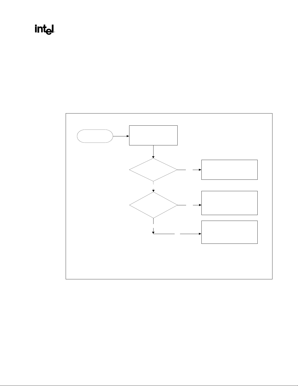
Intel® 815 Chipset: Graphics Controller PRM, Rev 1.0
R
2.3.1.2. System Startup
The Intel® 815 chipset has multiple possible device modes. The selection of which mode will be autodetected is represented in the following flow chart. The software requirements for implementing this high
level flow are detailed in the next section.
Multi-monitor configurations are not addressed, as that is a function of the operating system when
supported. System BIOS also provides the ability to select any of the display devices as the primary
display device.
Figure 4. Device Mode Auto-Detect Flowchart
System Reset
Memory and Basic
chipset Initialization
AGP Card
Detected?
No
Display Cache
(GPA Card)
Detected?
No
Yes
Yes
No
DEV#0, REG53H, Bit1=0
Display Cache on GPA
DEV#0, REG53H, BIT1=1
DEV#0, REG53H, BIT1=1
REG70H, BIT7:6=11 or 10
Mode 1
(AGP Card)
Mode 2
(Internal Graphics with
Card)
Mode 3
(Internal Graphics with
Shared Memory)
25
Page 26

Intel® 815 Chipset: Graphics Controller PRM, Rev 1.0
2.3.1.3. Software Start-Up Sequence
The following sequence of events will occur during the initialization of an Intel® 815 chipset-based
system:
1. The ICH asserts PCIRST# either in response to an initial assertion of PWROK or a write to an I/O
Port.
2. System BIOS runs basic POST code to test the processor.
3. System BIOS initializes the minimum set of Intel
initiate a PCI configuration cycle towards the AGP/PCI interface (e.g., bus #1). Note that
following a system reset condition, the Intel
Graphics disabled).
4. System BIOS detects if an AGP graphics card is present by attempting a configuration read cycle
to the Intel
®
815 chipset AGP/PCI interface. If the configuration cycle completes successfully, then
it is assumed that an external graphics device is present on the AGP interface, and the Intel
chipset remains in “AGP Mode” (APCONT[0] = 0). If the AGP/PCI configuration cycle results in
a Master Abort, then it is assumed no external AGP graphics device is present, and the System
BIOS programs the Intel
®
815 chipset to “Internal Graphics Mode” by setting APCONT[0] = 1.
During the same configuration cycle as setting the APCONT[0] to either 0 or 1, the BIOS should
set APCONT[2] (GFX AGP Select Lock) = 1 to lock the configuration mode.
5. System BIOS will then initialize the minimum set of the Intel
required to detect and test system memory.
6. System BIOS interrogates each System Memory DIMM via the Serial Presence Detect (SPD)
mechanism (ICH I2C cycles).
7. System BIOS determines if system configuration is capable of 133 MHz operation. Requirements
for 133 MHz operation include: the Intel
®
populated with up to two double-sided, or three single-sided, PC133-compliant DIMMs.
8. If system is 133 MHz capable (as determined by the previous step), System BIOS “upshifts” the
System Memory operating frequency from 100 MHz to 133 MHz as follows (Note that the Intel
815 chipset typically resets internally to 100 MHz SM operation):
a) Program external clock generator chip (i.e., “CK815”) for 133 MHz System Memory
clocking via ICH I2C port (Byte 3, Bit 0 set to 1).
b) Wait for 1 µs to allow the Clock Generator to stabilize the external System Memory clocks
(i.e., SCLK). Note that the Clock Generator must guarantee a “clean” Host Clock (HCLK)
during this entire transition!
c) Program Intel
®
815 chipset System Memory Frequency Select bit (GMCHCFG[2]) to 1 to
enable internal System Memory clocking to operate at 133 MHz.
d) Wait at least 0.5 µs for the Intel
accessing anything other than Intel
®
815 chipset to re-synchronize internal clocks before
®
interface/ICH interface.
9. System BIOS then detects and configures all of system memory, and tests enough memory to
support a stack and an interrupt area.
10. System BIOS should shadow itself and complete system initialization.
11. If and only if the Intel
®
815 chipset is in Internal Graphics Mode (APCONT[0] = 1), pass control
to the system BIOS internal graphics mode initialization routines described below.
12. System BIOS programs the Intel
®
815 chipset base addresses using PCI configuration cycles as
described in the PCI Local Bus Specification.
13. PCI enumeration takes place at this point.
®
815 chipset configuration registers required to
®
815 chipset will always be in “AGP Mode” (Internal
®
815 chipset configuration registers
815 chipset in AGP Mode, and System Memory
815 chipset Configuration registers or the Hub
®
815
R
®
26
Page 27

Intel® 815 Chipset: Graphics Controller PRM, Rev 1.0
R
14. During PCI enumeration, the system BIOS will identify and initialize the primary display device.
The selection of the primary display device is typically OEM dependent. An OEM may use a
BIOS setup question to allow the system user to select the primary display device. Intel
recommends the system BIOS to give preference to the higher performance display device when
performing an “auto-selection” of the primary display device. If the GMCH is in AGP mode, this
algorithm gives preference to the AGP graphics device over a PCI VGA device. If the Intel
®
815
chipset is in GFX mode, this algorithm gives preference to the internal graphics controller over a
PCI VGA device.
15. Once the primary display device has been initialized, system BIOS will pass control to the Video
Option ROM corresponding to that display device.
16. If and only if the GMCH is in GFX Mode (APCONT[0] = 1), the Video Option ROM will perform
initialization routines described below.
17. System BIOS then completes the system test including testing the rest of main memory.
The following System BIOS initialization steps only apply if the GMCH is in “Internal Graphics Mode”
(Not AGP):
1. System BIOS determines if a GPA card (i.e., Local Memory) is present. This is accomplished the
same as on the Intel
®
810 chipset: Enable Local Memory via the DRT, DRAMCL, and DRAMCH
(offsets 3000-3002h) and attempt to write and readback a location in Local Memory. If the
readback returns the same data that was written previously, then it can be assumed that Local
Memory is present. If a GPA card is present, the following additional steps take place:
• System BIOS configures the Local Memory Timing Options via the DRAMCL register at
Device 2 Memory Mapped Register offset 3001h. There is no Serial Presence Detect
mechanism available for the Local Memory / GPA Card interface, so the method used to
determine these timing options is entirely up to the OEM. One conservative option is to leave
the DRAMCL register with its default settings, which are the slowest available. Another
option is to enforce certain minimum timings on any GPA cards used by that OEM, and
program the DRAMCL with those minimums. While not recommended, it is also possible to
determine optimal timings empirically.
The following Video BIOS initialization steps only apply if the GMCH is in “Internal Graphics Mode”
(Not AGP):
1. Video BIOS assumes a VGA monitor type, and initializes the 2D-display controller in text mode.
2. 2D Video BIOS should take care to keep track of BIOS changes due to chip version changes.
3. The 3D section should be software-reset and initialized. At this point, no 3D operation should be
enabled, since this is done at the application/driver level.
2.3.1.3.1. Graphics Driver Startup
At this point the GMCH internal graphics controller has been configured and initialized. The remainder
of the graphics initialization occurs when the operating system calls the graphics driver. The graphics
driver must initialize the graphics component address re-mapping hardware. Tasks include:
1. Allocate memory for the GTT re-mapping table. Set the host memory type of graphics memory for
both physically local and system memory (i.e. enable Write Combining for local and non-local
memory: OS calls graphics driver which calls OS services for setting host memory type).
2. Establish policy for limiting the amount of non-local video memory. The OS determines the
maximum amount of system memory that can be allocated as non-local video memory. The
graphics driver can make a guess on what is likely to be provided by the OS based on the same
information that the OS uses to make its decision. The graphics driver can query the OS to check
the type of memory surface allocation (i.e., system vs. local vs. non-local video memory.)
27
Page 28

Intel® 815 Chipset: Graphics Controller PRM, Rev 1.0
3. After the conclusion of the graphics driver startup code the internal graphics functions will be
ready for run-time activity and commands can be written into the ring buffer.
2.3.1.4. Switching Device modes
Under normal conditions, the GMCH Device Mode will be switched at most once: from AGP to Internal
Graphics mode (via APCONT[0]) when no external AGP graphics device is present. This is handled
automatically by the system BIOS during system initialization. There is no case where the GMCH will be
switched from Internal Graphics mode to AGP mode.
R
28
Page 29
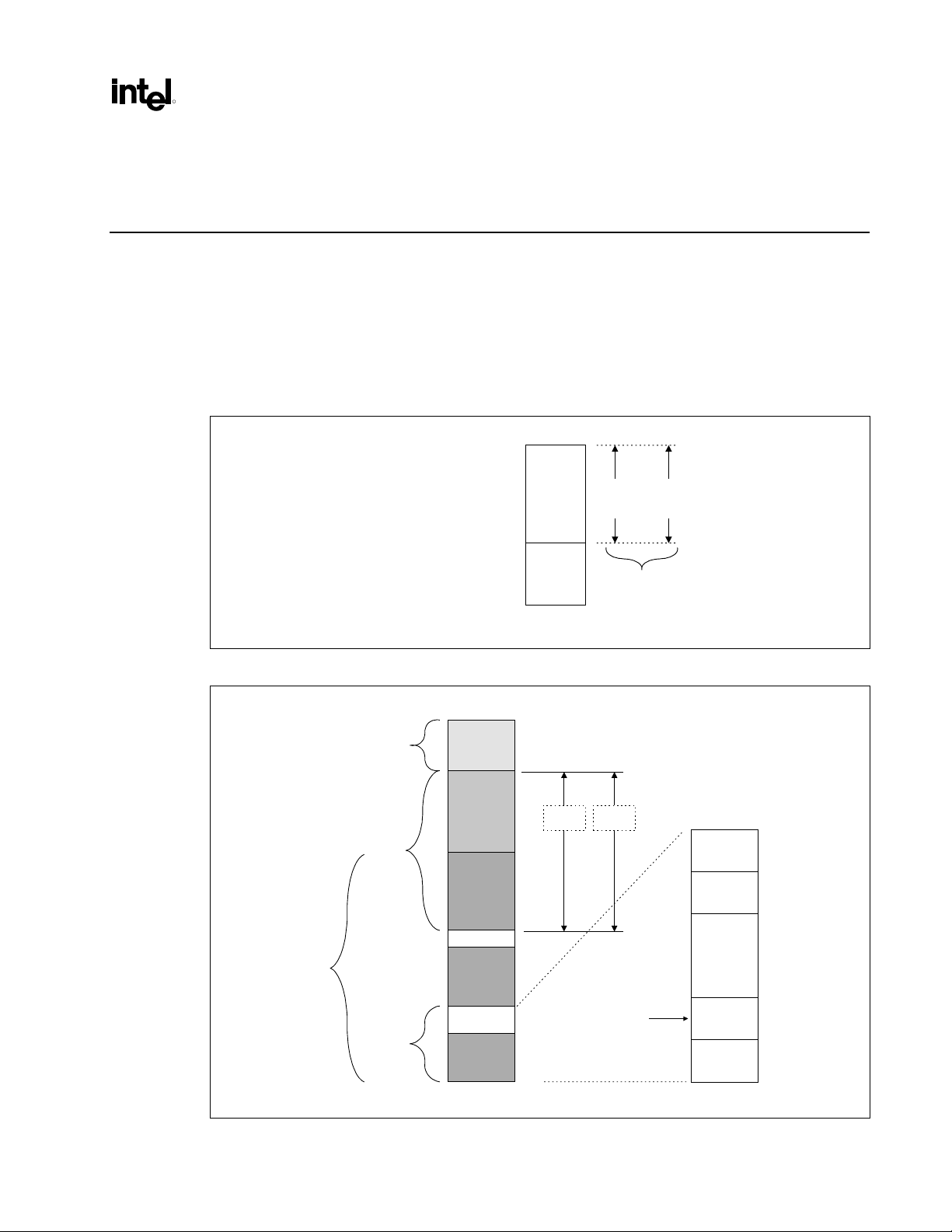
Intel® 815 Chipset: Graphics Controller PRM, Rev 1.0
s
y
R
3. System Address Map
This chapter provides address maps of the graphics controller (GC) I/O and memory-mapped registers.
Individual register bit field descriptions are provided in the following chapters. Note that PCI
configuration register descriptions are not covered in this document. For details on PCI configuration
registers, refer to the Intel® 815 Chipset: 82815 Graphics and Memory Controller (GMCH) EDS.
Figure 5 shows a high-level representation of the system memory address map. Figure 6 provides
additional details on mapping specific memory regions as defined and supported by the GMCH chipset.
Figure 5. System Memory Address Map
4 GB
PCI
Memory
Address
Range
Local
Memory
Range
Memory
Mapped
Range
Top of the Main Memory
0
Figure 6. Detailed Memory System Address Map
System Memor
Space
Extended
P6
Memory
PCI
Memory
Range
Optional ISA Hole
Main Memory
Range
DOS
Compatibility
Memory
Main
Memory
Address
Range
64 GB
4 GB Max TOM
AGP
Window
512 MB
16 MB
15 MB
1 MB
640 KB
0 MB
Independently
Programmable NonOverlapping Memory
Windows
mem_map_
Graphics
Aperture
Optionally
mapped to the
internal AGP
0FFFFFh 1 MB
0F0000h
0EFFFFh
0E0000h
0DFFFFh
0C0000h
0BFFFFh
0A0000h
09FFFFh
000000h
Upper BIOS Area
(64 KB)
Lower BIOS Area
(64 KB; 16 KB x 4)
Expansion Card
BIOS
and Buffer Area
(128 KB;
16 KB x 8)
Std PCI/ISA
Video Mem
(SMM Mem)
128 KB
DOS Area
(640 KB)
960 KB
896 KB
768 KB
640 KB
0 KB
mem_map2.vsd
29
Page 30
Intel® 815 Chipset: Graphics Controller PRM, Rev 1.0
a
e
3.1. Memory and I/O Space Registers
This section provides a high-level register map (register groupings per function). The memory and I/O
maps for the GC registers are shown in the following figure. The VGA and Extended VGA registers can
be accessed via standard VGA I/O locations as well as via memory-mapped locations. In addition, the
memory map contains allocation ranges for various functions. The memory space address listed for each
register is an offset from the base memory address programmed into the MMADR register (PCI
configuration offset 14h).
Figure 7. Graphics Controller Register Memory and I/O Map
Note:
1. Some Overlay registers are
double-buffered with an additional address
range in graphics memory. See Overlay
Register Chapter for details.
I/O Space Map
(Standard graphics locations)
Memory Space Map
(512 KB allocation)
- Cursor Registers
- Display Registers
- Pixel Pipe Registers
- TVout Registers
- Misc Multimedia Registers
Reserved
Blt Engine Control Status (RO)
Overlay Registers
Reserved
Page Table Range
Reserved
Clock Control Registers
Misc I/O Control Registers
Test & Diagnostic Registers
Local Memory Interface
Control Registers
- Instruction Control Regs.
- Fence Table Registers
- Interrupt Control
VGA and Ext. VGA RegistersVGA and Ext. VGA Registers
Offset From
Base_Reg
7FFFFh
70000h
6FFFFh
60000h
5FFFFh
50000h
4FFFFh
40000h
3FFFFh
1
30000h
2FFFFh
20000h
1FFFFh
10000h
0FFFFh
07000h
06FFFh
06000h
05FFFh
05000h
04FFFh
04000h
03FFFh
03000h
02FFFh
01000h
00FFFh
00000h
MMADR Regist
(Base Address)
R
1931
gfx_reg_m
30
Page 31

Intel® 815 Chipset: Graphics Controller PRM, Rev 1.0
R
• VGA and Extended VGA Control Registers (00000h−−−−00FFFh). These registers are located in
both I/O space and memory space. The VGA and Extended VGA registers contain the following
register sets: General Control/Status, Sequencer (SRxx), Graphics Controller (GRxx), Attribute
Controller (ARxx), VGA Color Palette, and CRT Controller (CRxx) registers. Detailed bit
descriptions are provided in the VGA and Extended VGA Register Chapter. The registers within a
set are accessed using an indirect addressing mechanism as described at the beginning of each
section. Note that some of the register description sections have additional operational information
at the beginning of the section.
• Instruction, Memory, Interrupt Control, and Error Registers (01000h−−−−02FFFh). The
Instruction and Interrupt Control registers are located in main memory space and contain the
following types of registers:
Instruction Control Registers. Ring Buffer registers and page table control registers are located
in this address range. Various instruction status, error, and operating registers are located in
this group of registers.
Graphics Memory Fence Registers. The Graphics Memory Fence registers are used for
memory tiling capabilities.
Interrupt Control/Status Registers. This register set provides interrupt control/status for various
GC functions.
Display Interface Control Register. This register controls the FIFO watermark and provides
burst length control.
• Local Memory Registers (03000h−−−−03FFFh). These registers are located in main memory space
and provide local memory DRAM control.
• Reserved (04000h−−−−04FFFh).
• Miscellaneous I/O Control Registers (05000h−−−−05FFFh). This chapter provides miscellaneous I/O
control register functions.
• Clock Control Registers (06000h−−−−06FFFh). This memory address space is the location of the GC
clock control and power management registers.
• Reserved (07000h−−−−0FFFFh).
• Page Table Range (10000h−−−−1FFFFh).
• Reserved (20000h−−−−2FFFFh).
• Overlay Registers (30000h−−−−3FFFFh). These registers provide control of the GC overlay engine.
The overlay registers are double-buffered with one register buffer located in graphics memory and
the other on the GC chip. On-chip registers are not directly writeable. To update the on-chip
registers software writes to the register buffer area in graphics memory and instructs the GC to
update the on-chip registers.
• Blitter Status Registers (40000h−−−−4FFFFh). For debug purposes only, a set of read-only registers
provide visibility into the BLT engine status.
• Reserved (50000h−−−−5FFFFh). (Reserved in the Intel
®
815 chipset).
• LCD/TV-Out Registers (60000h−−−−6FFFFh). This memory address range is used for LCD/TV-Out
control registers.
• Cursor, Display, and Pixel Pipe Registers (70000h−−−−7FFFFh). This memory address range is
used for cursor control, display, and pixel pipe control registers.
31
Page 32

Intel® 815 Chipset: Graphics Controller PRM, Rev 1.0
3.2. GC Register Memory Address Map
All GC registers are memory-mapped. In addition, the VGA and Extended VGA registers are I/O
mapped.
Table 2. Memory-Mapped Registers
Address Offset Symbol Register Name Access
00000h−00FFFh VGA and VGA Extended Registers
These registers are both memory and I/O mapped
and are listed in the following table. Note that the I/O
address and memory offset address are the same
value for each register.
Instruction and Interrupt Control Registers (01000h−−−−02FFFh)
01000h−01FFFh Reserved. Do not write
02000h−0201Fh FENCE[0:7] Graphics Memory Fence Table Register [0:7] R/W
02020h−02023h PGTBL_CTL Page Table Control Register R/W
02024h−02027h PGTBL_ER Page Table Error Register RO
02028h−0202Bh PGTBL_ERRMSK Page Table Error Mask Register R/W
02030h–0207Fh
02030h–0203Fh
02040h–0204Fh
02050h–0207Fh
02080h–02083h HWS_PGA Hardware Status Page Address Register R/W
02084h–02087h Reserved
02088h–0208Bh IPEIR Instruction Parser Error Identification Register RO
0208Ch–0208Fh IPEHR Instruction Parser Error Header Register RO
02090h–02091h INSTDONE Instruction Stream Interface Done Register RO
02092h–02093h Reserved
02094h–02097h NOPID NOP Identification Register RO
02098h−002099h HWSTAM Hardware Status Mask Register R/W
0209Ah–0209Fh Reserved
020A0h−020A1h IER Interrupt Enable Register R/W
020A2h–020A3h Reserved
020A4h−020A5h IIR Interrupt Identity Register R/WC
020A6h–020A7h Reserved
020A8h−020A9h IMR Interrupt Mask Register R/W
020AAh–020ABh Reserved
020ACh−020ADh ISR Interrupt Status Register RO
020AEh−020AFh Reserved
020B0h−020B1h EIR Error Identity Register R/WC
020B2h−020B3h Reserved
020B4h−020B5h EMR Error Mask Register R/W
020B6h−020B7h Reserved
020B8h−020B9h ESR Error Status Register RO
020BAh−020BFh Reserved
RINGBUF Ring Buffer Registers
Low Priority Ring Buffer (4 DWs)
Interrupt Ring Buffer (4 DWs)
Reserved
R/W
R
32
Page 33

Intel® 815 Chipset: Graphics Controller PRM, Rev 1.0
R
Table 2. Memory-Mapped Registers
Address Offset Symbol Register Name Access
020C0h INSTPM Instruction Parser Mode Register R/W
020C1h–020C3h Reserved
020C4h–020C7h INSTPS Instruction Parser State Register RO
020C8h–020CBh BBP_PTR Batch Buffer Parser Pointer Register RO
020CCh–020CFh ABB_SRT Active Batch Buffer Start Address Register RO
020D0h–020D3h ABB_END Active Batch Buffer End Address Register RO
020D4h–020D7h DMA_FADD DMA Engine Fetch Address Register RO
020D8h–020DBh FW_BLC FIFO Watermark and Burst Length Control R/W
020DCh–020DBh Reserved
020DCh–020DFh MEM_MODE Memory Interface Mode Register R/W
020E0h−02FFFh Reserved
Memory Control Registers (03000h−−−−03FFFh)
03000h DRT DRAM Row Type R/W
03001h DRAMCL DRAM Control Low R/W
03002h DRAMCH DRAM Control High R/W
03003h−03FFFh Reserved
Reserved (04000h−−−−04FFFh)
04000h−04FFFh Reserved
I/O Control Registers (05000h−−−−05FFFh)
05000h−05003h HVSYNC HSYNC/VSYNC Control R/W
05010h−05013h GPIOA General Purpose I/O Control A R/W
05014h−05017h GPIOB General Purpose I/O Control B R/W
05018h−05FFFh Reserved
Clock Control and Power Management Registers (06000h−−−−06FFFh)
06000h−06003h DCLK_0D Display Clock 0 Divisor R/W
06004h−06007h DCLK_1D Display Clock 1 Divisor R/W
06008h−0600Bh DCLK_2D Display Clock 2 Divisor R/W
0600Ch−0600Fh LCD_CLKD LCD Clock Divisor R/W
06010h−06013h DCLK_0DS Display and LCD Clock Divisor Select R/W
06014h−06017h PWR_CLKC Power Management and Miscellaneous Clock
Control
Reserved (07000h−−−−0FFFFh)
07000h−0FFFFh Reserved
Graphics Translation Table Range Definition (10000h−−−−1FFFFh)
R/W
10000h−1FFFFh GTT Graphics Translation Table Range Definition WO
Reserved (20000h−−−−2FFFFh)
20000h−2FFFFh Reserved
33
Page 34

Intel® 815 Chipset: Graphics Controller PRM, Rev 1.0
Table 2. Memory-Mapped Registers
Address Offset Symbol Register Name Access
Overlay Registers (30000h−−−−03FFFFh)
(For additional address offsets in the double-buffering scheme, see Overlay Chapter)
30000h−30003h OV0ADD Overlay 0 Register Update Address Overlay 0 R/W
30004h−30007h — Reserved —
30008h−3000Bh DOV0STA Display/Overlay 0 Status RO
3000Ch−3000Fh — Reserved —
30010h−30027h GAMMA[5:0] Gamma Correction [5:0] (6 registers) R/W
30028h−300FFh — Reserved —
30100h–30103 OBUF_0Y Overlay Buffer 0 Y Pointer RO
30104h−30107h OBUF_1Y Overlay Buffer 1 Y Pointer RO
30108h−3010Bh OBUF_0U Overlay Buffer 0 U Pointer RO
3010Ch−3010Fh OBUF_0V Overlay Buffer 0 V Pointer RO
30110h−30113h OBUF_1U Overlay Buffer 1 U Pointer RO
30114h−30117h OBUF_1V Overlay Buffer 1 V Pointer RO
30118h−3011Bh OV0STRIDE Overlay 0 Stride RO
3011Ch−3011Fh YRGB_VPH Y/RGB Vertical Phase RO
30120h−30123h UV_VPH UV Vertical Phase RO
30124h−30127h HORZ_PH Horzontal Phase RO
30128h−3012Bh INIT_PH Initial Phase RO
3012Ch−3012Fh DW INPOS Destination Window Position RO
30130h−30133h DWINSZ Destination Window Size RO
30134h−30137h SWID Source Width RO
30138h−3013Bh SWIDQW Source Width In QWords RO
3013Ch−3013Fh SHEIGHT Source Height RO
30140h−30143h YRGBSCALE Y/RGB Scale Factor RO
30144h−30147h UVSCALE U V Scale Factor RO
30148h−3014Bh OV0CLRC0 Overlay 0 Color Correction 0 ` RO
3014Ch−3014Fh OV0CLRC1 Overlay 0 Color Correction 1 RO
30150h−30153h DCLRKV Destination Color Key Value RO
30154h−30157h DCLRKM Destination Color Key Mask RO
30158h−3015Bh SCLRKVH Source Color Key Value High RO
3015Ch−3015Fh SCLRKVL Source Color Key Value Low RO
30160h−30163h SCLRKM Source Color Key Mask RO
30164h−30167h OV0CONF Overlay 0 Configuration RO
30168h−3016Bh OV0CMD Overlay 0 Command RO
30170h−30173h AWINPOS Alpha Blend Window Position RO
30174h−30177h AWINZ Alpha Blend Window Size RO
30178h−3FFFFh Reserved
R
34
Page 35

Intel® 815 Chipset: Graphics Controller PRM, Rev 1.0
R
Table 2. Memory-Mapped Registers
Address Offset Symbol Register Name Access
BLT Engine Status (40000h−−−−4FFFFh) (Software Debug)
40000h–40003h BR00 BLT Opcode and Control RO
40004h–40007h BR01 Setup BLT Raster OP, Control, and Destination
Offset
40008h–4000Bh BR02 Clip Rectangle Y1 Address RO
4000Ch–4000Fh BR03 Clip Rectangle Y1 Address RO
40010h–40013h BR04 Clip Rectangle X1 and X2 Address RO
40014h–40017h BR05 Setup Expansion Background Color RO
40018h–4001Bh BR06 Setup Expansion Foreground Color RO
4001Ch–4001Fh BR07 Setup Color Pattern Address RO
40020h–40023h BR08 Destination X1 and X2 RO
40024h–40027h BR09 Destination Address and Destination Y1 Address RO
40028h–4002Bh BR10 Destination Y2 Address RO
4002Ch–4002Fh BR11 BLT Source Pitch (Offset) or Monochrome Source
Quadwords
40030h–40033h BR12 Source Address RO
40034h–40037h BR13 BLT Raster OP Control, and Destination Pitch RO
40038h–4003Bh BR14 Destination W idth and Height RO
4003Ch–4003Fh BR15 Color Pattern Address RO
40040h–40043h BR16 Pattern Expansion Background and Solid Pattern
Color
40044h–40047h BR17 Pattern Expansion Foreground Color RO
40048h–4004Bh BR18 Source Expansion Background and Destination Colr RO
4004Ch–4004Fh BR19 Source Expansion Foreground Color RO
40074h–40077h SSLADD Source Scan Line Address RO
40078h–4007Bh DSLH Destination Scan Line Height RO
4007Ch–4007Fh DSLRADD Destination Scan Line Read Address RO
40080h–4FFFFh Reserved
RO
RO
RO
Reserved (50000h–5FFFFh)
50000h−5FFFFh Reserved
35
Page 36

Intel® 815 Chipset: Graphics Controller PRM, Rev 1.0
Table 2. Memory-Mapped Registers
Address Offset Symbol Register Name Access
LCD/TV-Out Registers (60000h–6FFFFh)
LCD/TV-Out
60000h–60003h HTOTAL Horizontal Total R/W
60004h–60007h HBLANK Horizontal Blank R/W
60008h–6000Bh HSYNC Horizontal Sync R/W
6000Ch–6000Fh VTOTAL Vertical Total R/W
60010h–60013h VBLANK Vertical Blank R/W
60014h–60017h VSYNC Vertical Sync R/W
60018h–6001Bh LCDTV_C LCD / TV-Out Control R/W
6001Ch–6001Fh OVRACT Overlay Active Register R/W
60020h–60023h BCLRPAT Border Color Pattern R/W
60024h−6FFFFh Reserved
Display and Cursor Control Registers (70000h–7FFFFh)
R
70000h–70003h DISP_SL Display Scan Line Count R/W
70004h–70007h DISP_SLC Display Scan Line Count Range Compare R/W
70008h–7000Bh PIXCONF Pixel Pipeline Configuration R/W
7000Ch–7000Fh BLTCNTL BLT Control R/W
70010h–70013h DIAG Diagnostic R/W
70014h–7001Fh SWF[1:3] Software Flags [1:3] (3 registers) R/W
70020h–70023h DPLYBASE Display Base Address R/W
70024h–70027h DPLYSTAS Display Status Select R/W
70080h–70083h CURCNTR Cursor Control and Vertical Extension R/W
70084h–70087h CURBASE Cursor Base Address R/W
70028h–7002Bh CURPOS Cursor Position R/W
7002Ch–7FFFFh Reserved
3.3. VGA and Extended VGA Register Map
For I/O locations, the value in the address column represents the register I/O address. For memory
mapped locations, this address is an offset from the base address programmed in the MMADR register
(PCI Configuration register).
36
Page 37

Intel® 815 Chipset: Graphics Controller PRM, Rev 1.0
R
3.3.1. VGA and Extended VGA I/O and Memory Register Map
Table 3. I/O and Memory Register Map
Address Register Name (Read) Register Name (Write)
2D Registers
3B0h–3B3h Reserved Reserved
3B4h VGA CRTC Index (CRX) (monochome) VGA CRTC Index (CRX) (monochome)
3B5h VGA CRTC Data (monochome) VGA CRTC Data (monochome)
3B6h–3B9h Reserved Reserved
3BAh VGA Status Register (ST01) VGA Feature Control Register (FCR)
3BBh–3BFh Reserved Reserved
3C0h VGA Attribute Controller Index (ARX) VGA Attribute Controller Index (ARX)/
3C1h VGA Attribute Controller Data
(read ARxx data)
3C2h VGA Feature Read Register (ST00) VGA Miscellaneous Output Register (MSR)
3C3h Reserved Reserved
3C4h VGA Sequencer Index (SRX) VGA Sequencer Index (SRX)
3C5h VGA Sequencer Data (SRxx) VGA Sequencer Data (SRxx)
3C6h VGA Color Palette Mask (DACMASK) VGA Color Palette Mask (DACMASK)
3C7h VGA Color Palette State (DACSTATE) VGA Color Palette Read Mode Index (DACRX)
3C8h VGA Color Palette Write Mode Index
(DACWX)
3C9h VGA Color Palette Data (DACDATA) VGA Color Palette Data (DACDATA)
3CAh VGA Feature Control Register (FCR) Reserved
3CBh Reserved Reserved
3CCh VGA Miscellaneous Output Register (MSR) Reserved
3CDh Reserved Reserved
3CEh VGA Graphics Controller Index (GRX) VGA Graphics Controller Index (GRX)
3CFh VGA Graphics Controller Data (GRxx) VGA Graphics Controller Data (GRxx)
3D0h–3D1h Reserved Reserved
VGA Attribute Controller Data (alternating
writes select ARX or write ARxx Data)
Reserved
VGA Color Palette Write Mode Index
(DACWX)
2D Registers
3D4h VGA CRTC Index (CRX) VGA CRTC Index (CRX)
3D5h VGA CRTC Data (CRxx) VGA CRTC Data (CRxx)
2D Registers
3D8h–3D9h Reserved Reserved
3DAh VGA Status Register (ST01) VGA Feature Control Register (FCR)
3DBh–3DFh Reserved Reserved
37
Page 38

Intel® 815 Chipset: Graphics Controller PRM, Rev 1.0
3.4. Indirect VGA and Extended VGA Register Indices
Programming an index value into the appropriate SRX, GRX, ARX, or CRX register indirectly accesses
the registers listed in this section. The index and data register address locations are listed in the previous
section. Additional details concerning the indirect access mechanism are provided in the VGA and
Extended VGA Registers Chapter (see SRxx, GRxx, ARxx or CRxx sections).
Table 4. 2D Sequence Registers (3C4h / 3C5h)
Index Sym Description
00h SR00 Sequencer Reset
01h SR01 Clocking Mode
02h SR02 Plane / Map Mask
03h SR03 Character Font
04h SR04 Memory Mode
07h SR07 Horizontal Character Counter Reset
Table 5. 2D Graphics Controller Registers (3CEh / 3CFh)
Index Sym Register Name
R
00h GR00 Set / Reset
01h GR01 Enable Set / Reset
02h GR02 Color Compare
03h GR03 Data Rotate
04h GR04 Read Plane Select
05h GR05 Graphics Mode
06h GR06 Miscellaneous
07h GR07 Color Don’t Care
08h GR08 Bit Mask
10h GR10 Address Mapping
11h GR11 Page Selector
14:1Fh GR[14:1F] Software Flags
38
Page 39

Intel® 815 Chipset: Graphics Controller PRM, Rev 1.0
R
Table 6. 2D Attribute Controller Registers (3C0h / 3C1h)
Index Sym Register Name
00h AR00 Palette Register 0
01h AR01 Palette Register 1
02h AR02 Palette Register 2
03h AR03 Palette Register 3
04h AR04 Palette Register 4
05h AR05 Palette Register 5
06h AR06 Palette Register 6
07h AR07 Palette Register 7
08h AR08 Palette Register 8
09h AR09 Palette Register 9
0Ah AR0A Palette Register A
0Bh AR0B Palette Register B
0Ch AR0C Palette Register C
0Dh AR0D Palette Register D
0Eh AR0E Palette Register E
0Fh AR0F Palette Register F
10h AR10 Mode Control
11h AR11 Overscan Color
12h AR12 Memory Plane Enable
13h AR13 Horizontal Pixel Panning
14h AR14 Color Select
Table 7. 2D CRT Controller Registers (3B4h / 3D4h / 3B5h / 3D5h)
Index Sym Register Name
00h CR00 Horizontal Total
01h CR01 Horizontal Display Enable End
02h CR02 Horizontal Blanking Start
03h CR03 Horizontal Blanking End
04h CR04 Horizontal Sync Start
05h CR05 Horizontal Sync End
06h CR06 Vertical Total
07h CR07 Overflow
08h CR08 Preset Row Scan
09h CR09 Maximum Scan Line
0Ah CR0A Text Cursor Start
0Bh CR0B Text Cursor End
0Ch CR0C Start Address High
0Dh CR0D Start Address Low
0Eh CR0E Text Cursor Location High
39
Page 40

Intel® 815 Chipset: Graphics Controller PRM, Rev 1.0
Index Sym Register Name
0Fh CR0F Text Cursor Location Low
10h CR10 Vertical Sync Start
11h CR11 Vertical Sync End
12h CR12 Vertical Display Enable End
13h CR13 Offset
14h CR14 Underline Location
15h CR15 Vertical Blanking Start
16h CR16 Vertical Blanking End
17h CR17 CRT Mode
18h CR18 Line Compare
22h CR22 Memory Read Latch Data
30h CR30 Extended Vertical Total
31h CR31 Extended Vertical Display End
32h CR32 Extended Vertical Sync Start
33h CR33 Extended Vertical Blanking Start
35h CR35 Extended Horizontal Total Time
39h CR39 Extended Horizontal Blank Time
40h CR40 Extended Start Address
41h CR41 Extended Offset
42h CR42 Extended Start Address High
70h CR70 Interlace Control
71h CR71 NTSC/PAL Video Output Control
72h CR72 Horizontal Serration 1 Start
73h CR73 Horizontal Serration 2 Start
74h CR74 NTSC/PAL Horizontal Pulse W idth
75h CR75 TV-Out Control
76h CR76 TV-Out Horizontal Count Upper
77h CD77 TV-Out Horizontal Count Lower
78h CR78 TV-Out Vertical Count Upper
79h CR79 TV-Out Vertical Count Lower
80h CR80 I/O Control
81h CR81 Reserved
82h CR82 Blink Rate Control
R
40
Page 41

Intel® 815 Chipset: Graphics Controller PRM, Rev 1.0
R
3.4.1. Graphics Address Translation
The Intel® 815 chipset uses a logical memory-addressing concept for accessing graphics data. The GC
supports a 64-MB logical address space, where each 4-KB logical page can be mapped to a physical
memory page in System RAM, PCI Memory, or an optional Display Cache memory. This mapping is
performed through the use of a Graphics Translation Table (GTT).
GC engines can address the full 64-MB logical address space. The processor is provided access to either
the full 64-MB space, or just the lower 32 MB, via a PCI memory range associated with the graphics
device.
The GTT is allocated in system RAM and maintained by the graphics driver. The 4 KB-aligned physical
address of the 64 KB GTT is programmed via the GC’s PGTBL register.
Each of the 16K DWord GTT entries can map a 4-KB logical page to a physical memory page. Fields in
the GTT entry control the mapping of that logical page in the following manner:
• (V) whether or not that logical 4 KB page is mapped to a physical memory page. Accesses to
invalid pages will result in an error interrupt.
• (T1T0) the physical memory address space of the mapped page:
System RAM page (no processor cache snoop)
PCI Memory page (processor cache snooped if below TOM)
Display Cache page
• the page number of the mapped page (within the particular physical memory address space)
Although the GTT format permits any logical page to be mapped to any page in the supported physical
memory address spaces, the GC imposes restrictions on how specific graphics operands (buffers, etc.)
can be mapped to physical memory.
The GTT entries must be written via a GTT alias in the graphics device’s memory-mapped register space
(10000h–1FFFFh). This allows the GC to snoop GTT entry writes and invalidate graphics TLBs as
required. The GTT entries must not be written directly in system memory.
41
Page 42

Intel® 815 Chipset: Graphics Controller PRM, Rev 1.0
d
Figure 8. GTT Mapping
System Memory
31 0
4 GB
Base + 64 MB
Virtual
Graphics
Memory
Base
TOM
4 KB
4 KB
Translation Table
31 0 31 0
Base + 32 MB
GTT Maps 4KB blocks of Virtual
Graphics Memory to 4 KB pages in
System Memory
Graphics
(GTT)
64 KB
0 KB
GTT Maps 4KB blocks of
Virtual Graphics Memory
to 4 KB pages in Display
Cache
Graphics Engine
Address Space
Optional Display
Cache
64 MB
0
R
3.4.2. Memory Buffers for GC’s Instruction Interface
The GC provides two Ring Buffer (RB) mechanisms through which instructions can be passed to the
GMCH’s Instruction Parser. In addition, the GC provides for the execution of instruction sequences
external to the ring buffers. These sequences are called "batch buffers", and are initiated through the use
of GFXCMDPARSER_BATCH_BUFFER instructions that specify the starting address and length of the
batch buffers. For detailed information on these buffers, refer to the Programming Interface Chapter.
gtt.vs
42
Page 43

Intel® 815 Chipset: Graphics Controller PRM, Rev 1.0
R
4. Graphics Translation Table (GTT) Range Definition
Address Offset: 10000h–FFFFh
Default Value: Page table range 64 KB
Access: aligned DWord-QWord Write Only
This range defined within the graphics memory mapped register space is for the memory manager to
access the graphics translation table. A page table write will invalidate that entry in internal translation
table caches (TLBs). The translation table resided in system memory and can be accessed by the memory
manager directly. However, to ensure coherency between hardware maintained translation caches and the
translation table in main memory, the memory manager must use this range to update the translation
table.
The page table is required to be QW aligned with each entry being DWord aligned such that each QW
stores the translation for 2, 4 KB pages. Page Table base address for graphics memory is programmed in
the PGTB_CNTL register. For graphics memory of 64 MB with a TLB block size of 4 KB, 16K entries
are needed. Each entry is 4 bytes; hence, the page table size is 64 KB.
Page Table Entry: 1 DWord per 4-KB page.
31 30 29 12 11 3 2 1 0
XX=00 Physical Address 29:12 Reserved T1T0 V
V: 1 = Valid page table entry (PTE).
0 = Invalid page table entry (PTE). An access to an invalid PTE will result in an interrupt.
T1T0: 01 = Physical address targets Local Memory
00 = Physical address targets main memory (not snooped)
11 = Physical address targets cacheable main memory (results in snoop on processor bus)
10 = Reserved.
Note: T1T0 = 11 is used only if the surface is a Blit soure or destination operand used within the context of a
source copy command.
Note that the 4-KB pages of physical main memory (that have been mapped to the graphics aperture
through the GTT) must be accessed strictly through the aperture. The GMCH does not guarantee data
coherency if any of these pages are accessed directly using their physical addresses. For example, a 4-KB
page of main memory has been mapped via the GTT to a 4-KB aperture page. Although, the GMCH still
allows this 4-KB page to be accessed directly through its physical memory address, the chipset does not
guarantee data coherency with respect to accesses through the normal graphics aperture address range.
This is because a read to the aperture memory can result in prefetching and caching of data, while a write
to the aperture can result in temporary write data buffering in the graphics controller of the GMCH.
Accesses to these same memory locations through their physical address take a different logical path
through the chipset controller side of the GMCH. There is no hardware support for ensuring coherency
between these two access paths.
43
Page 44

Intel® 815 Chipset: Graphics Controller PRM, Rev 1.0
This page is intentionally left blank.
R
44
Page 45

Intel® 815 Chipset: Graphics Controller PRM, Rev 1.0
R
5. Basic Initialization Procedures
5.1. Initialization Sequence
The initialization of graphics driver resources can be broken down into three categories: hardware
detection, frame buffer initialization, and hardware register initialization. Each category is discussed in
more detail in the following sections.
In all discussions that follow, there is a basic assumption that the graphics adapter has completed the
power-on video BIOS initialization or video BIOS reset. Therefore, the adapter is in a known state and
will respond in compliance with the VGA and VESA specifications.
5.2. Hardware Detection (Probe)
Most operating systems will probe for installed devices. The Intel 8281x family of devices advertise their
presence in PCI space by using unique values in the PCI VendorId and DeviceId locations. The
following table lists the device IDs used to identify the members of the 8281x family of graphics
adapters.
Vendor Id
PCI Offset: 0
8086 7120 0 Intel® 82810 chipset bridge
8086 7121 1 Intel® 82810 chipset
8086 7122 0 Intel® 82810 chipset DC100 bridge
8086 7123 1 Intel® 82810 chipset DC100
8086 7124 0 Intel® 82810E chipset bridge
8086 7125 1 Intel® 82810E chipset
8086 1100 0 Intel® 82815 chipset GMCH host-hub interface bridge /
8086 1101 1 Intel® 82815 chipset FSB limited to 100 MHz; AGP bridge
8086 1102 2 Intel® 82815 chipset FSB limited to 100 MHz; Internal graphics
8086 1110 0 Intel® 82815 chipset no AGP, internal graphics only; GMCH host-
8086 1112 2 Intel® 82815 chipset no AGP, internal graphics only; Internal
8086 1120 0 Intel® 82815 chipset no internal graphics, AGP only; GMCH host-
8086 1121 1 No internal graphics, AGP only; AGP bridge
8086 1130 0 Intel® 82815 chipset fully featured; GMCH host-hub interface
8086 1131 1 Intel® 82815 chipset fully featured; AGP bridge
8086 1132 2 Intel® 82815 chipset fully featured; Internal graphics device
Device Id
PCI Offset: 2
PCI Device
Number
Characteristics
DRAM controller FSB limited to 100 MHz
device
hub interface bridge / DRAM controller
graphics device
hub interface bridge / DRAM controller
bridge / DRAM controller
45
Page 46

Intel® 815 Chipset: Graphics Controller PRM, Rev 1.0
Once the operating system has identified the device, it can load the appropriate driver.
One of the first tasks of the driver is to make sure that the device matches the driver. Checking that the
driver and device match is done in much the same way that the operating system identifies the graphics
adapter. That is, the PCI VendorId and ProductId values are examined. Some operating systems will
make available to the driver the values it found during its scan. If not, the driver must scan the PCI space
until it finds a match on the VendorId and ProductId values. The driver normally caches this information
so that it is accessible by other driver modules, when needed.
The next task of the device driver is to ensure that required resources are present. These resources
include the minimum memory requirements, IO address space requirements, and operating system
support requirements (such as GART support). If the driver detects that the operating system or the
physical hardware does not meet the driver’s minimum requirements, the driver should not load. The
operating system should then be able to make use of the graphics adapter in its VGA- and VESAcompliant mode.
If the operating system and hardware support are present, the driver should acquire the blocks of memory
and IO address space that will be required. These blocks should include at least the following:
• Memory-mapped IO address space: 512 KB beginning at 0x80000
• Linear frame buffer space: 32 or 64 MB beginning at 0xFE000000
• Legacy IO addresses to support monochrome or color monitors
• VGA IO addresses
R
5.3. Frame Buffer Initialization
The frame buffer initialization is responsible for setting up the memory that will contain the display data.
Other objects also can be stored in display memory.
The following steps should be performed:
• Map a 0x80000-byte region in memory to the MMIO base address. The base address of the
memory-mapped region should be programmed into the MMADDR register, offset 14 in the PCI
address space.
• Allocate enough memory for the frame buffer from a memory pool created during initialization. The
amount of memory is determined by system characteristics, but should default to at least 8 MB.
• If a hardware cursor is being used, allocate memory for the hardware cursor from the same memory
pool. The hardware does not use the GART to access the memory for the cursor, so local-tophysical memory address translation must be performed. The hardware cursor memory address
should be programmed into the CURBASE register, memory-mapped address 70084h.
• The low-priority ring buffer memory should be initialized to 0. The low-priority ring buffer pointers
should be programmed into the ring buffer pointer registers, RINGBUF, which begin at offset
2030h in the memory-mapped IO space.
46
Page 47

Intel® 815 Chipset: Graphics Controller PRM, Rev 1.0
R
5.4. Hardware Register Initialization
5.4.1. Color vs. Monochrome Monitors
The mapping and initialization of some hardware registers depends in part on whether the graphics
adapter is attached to a monochrome or color monitor. The following steps illustrate how to determine
the type of output device attached to the graphics adapter:
• Read the Miscellaneous Output Register (0x3CC).
• Test the low-order bit of the Miscellaneous Output Register, and interpret it as follows:
0: The adapter is in monochrome monitor mode. In this mode, the control register is 3B4 and
3B5, and status is at 3BA.
1: The adapter is in color monitor mode. In this mode, the control register is 3D4 and 3D5,
and status is at 3DA.
See the section on VGA compatibility for a description of the register space that must be acquired.
5.4.2. Protect Registers: Locking and Unlocking
To make use of some protected VGA registers, a locking and unlocking mechanism needs to be
implemented. The following steps illustrate how to unlock (or unprotect) the VGA registers:
• Send a VERT_SYNC_END value to the register at vgaBase + 4.
• Read the value in the register at vgaBase + 5.
• Clear the high-order bit of the value just read.
• Write the resulting value back into the register at vgaBase + 5.
5.4.3. Checking Memory Frequency
The driver behavior occasionally must be modified, depending on the frequency at which the memory is
running. The following steps illustrate how to determine the local memory frequency:
®
• Read the contents of the Intel
• Examine the value of bit 4.
• The value is interpreted as follows:
0: Frequency is 100 MHz.
1: Frequency is 133 MHz.
82815 chipset Configuration Register (PCI address space 0x50).
5.5. Hardware State
Under certain conditions, it may be necessary to save and restore the hardware state of the graphics
adapter. These conditions include mode switching, output device switching, processing changes in power
state, and others. The next two sections provide a brief description of the state saving and restoration
requirements.
47
Page 48

Intel® 815 Chipset: Graphics Controller PRM, Rev 1.0
5.6. Saving the Hardware State
Note that the VGA register unlocking protocol must be performed in order to access some of the registers
described below.
During a state change, the driver should preserve the following registers to provide complete state
restoration in the future:
• IO Control CR80
• Address Mapping GR10
• Bit Blit Control MM 0x7000C
• Video Clock 2 / M MM 0x6008
• Video Clock 2 / N MM 0x600C
• Video Clock 2 / Divisor Select MM 0x6012
• Vertical Total CRX 30
• Vertical Display End CRX 31
• Vertical Sync Start CRX 32
• Vertical Blank Start CRX 33
• Horizontal Total CRX 35
• Horizontal Blnk CRX 39
• Ext Offset CRX 41
• Interlace Control CRX 70
• Hardware Status Mask Register MM 0x2098
• Interrupt Enable Register MM 0x20A0
• Interrupt Identity Register MM 0x20A4
• Interrupt Mask Register MM 0x20A8
• Error Mask Register MM 0x20B4
• Display Control Register MM 0x70008
• Pixel Pipeline Configuration 0 Register MM 0x70009
• Pixel Pipeline Configuration 1 Register MM 0x7000A
• Pixel Pipeline Configuration 2 Register MM 0x7000B
• Watermark and Burstlength Control MM 0x20D8
• Low-priority ring information MM 0x2030 – 0x203F
R
48
Page 49

Intel® 815 Chipset: Graphics Controller PRM, Rev 1.0
R
5.7. Restoring the Hardware State
The graphics adapter state should be restored by performing the following steps. Note some of the
synchronization operations, especially those that ensure that the local memory is idle during the state
restore. Also, much of the work involves reprogramming the registers with the values captured during the
save-state operation.
• Blank the screen.
• Turn off DRAM refresh.
Read the value of the DRAM_CONTROL_HI Register (MM 0x3002).
Set the DRAM Refresh Rate bits (DDR Bits 4:3) to Disable_Refresh (value 0).
Write the modified value back to the DRAM_CONTROL_HI Register.
• Write the M, N, and P (i.e., the Divisor Select value) values from the saved state information.
• Restore the 8-bit DAC mode to what it was when the state was saved, but preserve the current value
of the rest of the register containing this flag:
Read the Pixel Pipeline Configuration 0 Register.
Clear the current value of the 8- or 6-bit DAC mode.
OR–in (only) the value of the DAC_8_BIT from saved register information of the Pixel
Pipeline Configuration 0 Register.
Write the result back to the Pixel Pipeline Configuration 0 Register.
• Restore the generic VGA registers to the values captured at save-state time.
• Restore the following registers to their saved state values:
Vertical Total CRX 30
Vertical Display End CRX 31
Vertical Sync Start CRX 32
Vertical Blank Start CRX 33
Horizontal Total CRX 35
Horizontal Blnk CRX 39
Ext Offset CRX 41
• The following registers should restore only certain bits from the saved state values:
Interlace Control CRX 70
Read the current value.
Clear the interlace enable bit.
OR–in the saved value of the Interlace Control Register.
Write the result back into the Interlace Control Register.
Address Mapping: GR10
Read the current value of the Address Mapping Register.
Save only the reserved bits values (bits 7:5).
OR–in the saved value of the Address Mapping Register.
Write the result back into the Address Mapping Register.
• Now the DRAM refresh can be turned on:
Read the value of the DRAM_CONTROL_HI Register.
Turn off the DRAM_REFRESH_RATE bits.
OR–in a 60-Hz refresh rate value.
Write the result back into the DRAM_CONTROL_HI Register.
49
Page 50

Intel® 815 Chipset: Graphics Controller PRM, Rev 1.0
• Other registers that should restore only certain bits from the saved-state values:
Bit Blit Control MM 0x7000c
Read the current value of the Bit Blit Control Register.
Clear the bits pertaining to the Color Expansion Mode (bits 5:4).
OR–in the saved value of the Bit Blit Control Register.
Write the result back into the Bit Blit Control Register.
Display Control Field MM 0x70008
Read the current value of the Display Control Register.
OR–in the saved value of the Display Control Register.
Write the result back into the Display Control Register.
Pixel Pipeline Configuration 0 Field MM 0x70009
Read the current value of the Pixel Pipeline Configuration 0 Register.
Save reserved bits 6:5 and 2. Clear all other bits.
OR–in the saved value of the Pixel Pipeline Configuration 0 Register.
Write the result back into the Pixel Pipeline Configuration 0 Register.
Pixel Pipeline Configuration 2 Field MM 0x7000b
Read the current value of the Pixel Pipeline Configuration 2 Register.
Save reserved bits 7:4 and 1:0. Clear all other bits.
OR–in the saved value of the Pixel Pipeline Configuration 2 Register.
Write the result back into the Pixel Pipeline Configuration 2 Register.
Pixel Pipeline Configuration 1 Field MM 0x7000a
Read the current value of the Pixel Pipeline Configuration 1 Register.
Clear the Display Color Mode bit (bits 3:0).
OR–in the saved value of the Pixel Pipeline Configuration 1 Register.
Write the result back into the Pixel Pipeline Configuration 1 Register.
Hardware Status Mask Register MM 0x2098
Read the current value of the Hardware Status Mask Register.
Clear everything but the reserved bits (14:13).
OR–in the saved value of the Hardware Status Mask Register.
Write the result back into the Hardware Status Mask Register.
Interrupt Enable Register MM 0x20A0
Read the current value of the Interrupt Enable Register.
Clear everything but the reserved bits (14:13).
OR–in the saved value of the Interrupt Enable Register.
Write the result back into the Interrupt Enable Register.
Interrupt Mask Register MM 0x20A8
Read the current value of the Interrupt Mask Register.
Clear everything but the reserved bits (14:13).
OR–in the saved value of the Interrupt Mask Register.
Write the result back into the Interrupt Mask Register.
Error Mask Register MM 0x20B4
Read the current value of the Error Mask Register.
Clear everything but the reserved bits (15:6).
OR–in the saved value of the Error Mask Register.
Write the result back into the Error Mask Register.
R
50
Page 51

Intel® 815 Chipset: Graphics Controller PRM, Rev 1.0
R
Watermark and Burstlength Control MM 0x20D8
Read the current value of the Watermark and Burstlength Control Register.
Clear the burst length and watermark bits (bits 22:20, 17:12, 10:8 and 5:0).
OR–in the saved value of the Watermark and Burstlength Control Register.
Write the result back into the Watermark and Burstlength Control Register.
• Disable the low-priority ring buffer, in preparation for setting new values, by clearing the
RING_VALID bit in the Low-Priority Ring Buffer Length field at MM 0x203C.
Read the current value of the Low-Priority Ring Buffer Length field (MM 0x203C).
Clear the valid bit (bit 0).
Write the result back into the Low-Priority Ring Buffer Length field.
• Set up the low-priority ring buffer.
Write a 0 to the low-priority ring buffer tail at MM 0x2030.
Write a 0 to the low-priority ring buffer head at MM 0x2034.
Restore the low-priority ring buffer start at MM 0x2038, but preserve the reserved bits.
Restore the Low-Priority Ring Buffer Length field, but preserve the Automatic Report Header
Pointer bits and set the Ring Buffer Valid flag.
• Turn on the screen.
• Relock the protected register space in order to complete the state restoration process.
At this point the graphics adapter should function completely, in the mode identified by the saved-state
information.
51
Page 52

Intel® 815 Chipset: Graphics Controller PRM, Rev 1.0
This page is intentionally left blank.
R
52
Page 53

Intel® 815 Chipset: Graphics Controller PRM, Rev 1.0
R
6. Blt Engine Programming
6.1. BLT Engine Programming Considerations
6.1.1. When the Source and Destination Locations Overlap
It is possible to have BLT operations in which the locations of the source and destination data overlap.
This frequently occurs in BLT operations where a user is shifting the position of a graphical item on the
display by only a few pixels. In these situations, the BLT engine must be programmed so that destination
data is not written into destination locations that overlap with source locations before the source data at
those locations has been read. Otherwise, the source data will become corrupted.
The following figure shows how the source data can be corrupted when a rectangular block is copied
from a source location to an overlapping destination location. The BLT engine reads from the source
location and writes to the destination location starting with the left-most pixel in the top-most line of
both, as shown in step (a). As shown in step (b), corruption of the source data has already started with the
copying of the top-most line in step (a) — part of the source that originally contained lighter-colored
pixels has now been overwritten with darker-colored pixels. More source data corruption occurs as steps
(b) through (d) are performed. At step (e), another line of the source data is read, but the two right-most
pixels of this line are in the region where the source and destination locations overlap, and where the
source has already been overwritten as a result of the copying of the top-most line in step (a). Starting in
step (f), darker-colored pixels can be seen in the destination where lighter-colored pixels should be. This
errant effect occurs repeatedly throughout the remaining steps in this BLT operation. As more lines are
copied from the source location to the destination location, it becomes clear that the end result is not
what was originally intended.
53
Page 54

Intel® 815 Chipset: Graphics Controller PRM, Rev 1.0
Figure 9. Source Corruption in BLT with Overlapping Source and Destination Locations
(b)
Source
(c)
(a)
Destination
(d)
(e)
R
(f)
Source
(g)
(i)
(h)
Destination
b_blt2.vsd
54
Page 55

Intel® 815 Chipset: Graphics Controller PRM, Rev 1.0
R
The BLT engine can alter the order in which source data is read and destination data is written when
necessary to avoid source data corruption problems when the source and destination locations overlap.
The command packets provide the ability to change the point at which the BLT engine begins reading
and writing data from the upper left-hand corner (the usual starting point) to one of the other three
corners. The BLT engine may be set to read data from the source and write it to the destination starting at
any of the four corners of the panel.
Figure 10. Correctly Performed BLT with Overlapping Source and Destination Locations
(b)
Source
(c)
(a)
Destination
(d)
(e)
(f)
Source
(g)
(i)
(h)
Destination
b_blt3.vsd
55
Page 56

Intel® 815 Chipset: Graphics Controller PRM, Rev 1.0
n
n
The figure below illustrates how this feature of the BLT engine can be used to perform the same BLT
operation as was illustrated in the figure above, while avoiding the corruption of source data. As shown
in the figure below, the BLT engine reads the source data and writes the data to the destination starting
with the right-most pixel of the bottom-most line. By doing this, no pixel existing where the source and
destination locations overlap will ever be written to before it is read from by the BLT engine. By the time
the BLT operation has reached step (e) where two pixels existing where the source and destination
locations overlap are about to be over written, the source data for those two pixels has already been read.
Figure 11. Suggested Starting Points for Possible Source & Destination Overlap Situations
Destination
Source
Destination Source
Destination Destination
OR
Source Source
Source
Destinatio
DestinationSource
R
OR
Destination Source
Destination
Source
Source Source
OR
Destination Destination
Source
OR
DestinationSource
Destinatio
b_blt4.vsd
The figure above shows the recommended lines and pixels to be used as starting points in each of 8
possible ways in which the source and destination locations may overlap. In general, the starting point
should be within the area in which the source and destination overlap.
56
Page 57

Intel® 815 Chipset: Graphics Controller PRM, Rev 1.0
R
6.2. Basic Graphics Data Considerations
6.2.1. Contiguous vs. Discontinuous Graphics Data
Graphics data stored in memory, particularly in the frame buffer of a graphics system, has organizational
characteristics that often distinguish it from other varieties of data. The main distinctive feature is the
tendency for graphics data to be organized in a discontinuous block of graphics data made up of multiple
sub-blocks of bytes, instead of a single contiguous block of bytes.
Figure 12. Representation of On-Screen Single 6-Pixel Line in the Frame Buffer
(0, 0)
256, 256 261, 256
256th Scan Line
Note: Drawing is not to scale
(0, 479) (639, 479)
(639, 0)
63
32 31 0
b_blt5.vsd
270F8h
28100h
28108h
The figure above shows an example of contiguous graphics data — a horizontal line made up of six
adjacent pixels within a single scan line on a display with a resolution of 640x480. Presuming that the
graphics system driving this display has been set to 8 bits per pixel, and that the frame buffer’s starting
address of 0h corresponds to the upper left-most pixel of this display, then the six pixels that make this
horizontal line starting at coordinates (256, 256) would occupy six bytes starting at frame buffer address
28100h, and ending at address 28105h.
In this case, there is only one scan line’s worth of graphics data in this single horizontal line, so the block
of graphics data for all six of these pixels exists as a single, contiguous block comprised of only these six
bytes. The starting address and the number of bytes are the only pieces of information that a BLT engine
would require to read this block of data.
The simplicity of the above example of a single horizontal line contrasts sharply to the example of
discontinuous graphics data depicted in the figure below. The simple six-pixel line of the figure above is
now accompanied by three more six-pixel lines placed on subsequent scan lines, resulting in the 6x4
block of pixels shown.
57
Page 58

Intel® 815 Chipset: Graphics Controller PRM, Rev 1.0
Figure 13. Representation of On-Screen 6x4 Array of Pixels in the Frame Buffer
(0, 0)
256, 256 261, 256
256th Scan Line
257th Scan Line
258th Scan Line
259th Scan Line
256, 259 261, 259
Note: Drawing is not to scale
(0, 479) (639, 479)
(639, 0)
63
32 31 0
b_blt6.vsd
270F8h
28100h
28108h
270F8h
28100h
28108h
270F8h
28100h
28108h
270F8h
28100h
28108h
R
Since there are other pixels on each of the scan lines on which this 6x4 block exists that are not part of
this 6x4 block, what appears to be a single 6x4 block of pixels on the display must be represented by a
discontinuous block of graphics data made up of 4 separate sub-blocks of six bytes apiece in the frame
buffer at addresses 28100h, 28380h, 28600h, and 28880h. This situation makes the task of reading what
appears to be a simple 6x4 block of pixels more complex. However, there are two characteristics of this
6x4 block of pixels that help simplify the task of specifying the locations of all 24 bytes of this
discontinuous block of graphics data: all four of the sub-blocks are of the same length, and the four subblocks are separated from each other at equal intervals.
The BLT engine is designed to make use of these characteristics of graphics data to simplify the
programming required to handle discontinuous blocks of graphics data. For such a situation, the BLT
engine requires only four pieces of information: the starting address of the first sub-block, the length of a
sub-block, the offset (in bytes), pitch, of the starting address of each subsequent sub-block, and the
quantity of sub-blocks.
6.2.2. Source Data
The source data may exist in the frame buffer or main memory graphics memory where the BLT engine
may read it directly, or it may be provided to the BLT engine by the host processor through the command
packets. The block of source graphics data may be either contiguous or discontinuous, and may be either
in color (with a color depth that matches that to which the BLT engine has been set) or monochrome.
The source select bit in the command packets specifies whether the source data exists in the frame buffer
or is provided through the command packets. Monochrome source data is always specified as being
supplied through an immediate command packet.
58
Page 59

Intel® 815 Chipset: Graphics Controller PRM, Rev 1.0
R
If the color source data resides within the frame buffer or main memory graphics memory, then the
Source Address Register, specified in the command packets is used to specify the address of the source.
However, if the host processor provides the source data, then this register takes on a different function
and the three least-significant bits of the Source Address Register can be used to specify a number of
bytes that must be skipped in the first quadword received from the command packet to reach the first
byte of valid source data.
In cases where the host processor provides the source data, it does so by writing the source data to ring
buffer directly after the BLT command that requires the data or uses an IMMEDIATE_INDIRECT_BLT
command packet which has a size and pointer to the operand in Main memory graphics memory.
There is also an address space used for debug where the processor can write the source data. It is a 64KB memory space on the host bus. There is no actual memory allocated to this memory space, so any
data that is written to this location cannot be read back. This memory space is simply a range of memory
addresses that the BLT engine’s address decoder watches for the occurrence of any memory writes.
The BLT engine loads all data written to any memory address within this memory space or through the
command packet in the order in which it is written, regardless of the specific memory address to which it
is written and uses that data as the source data in the current BLT operation. The block of bytes sent by
the host processor to either this data port or through the command packets must be quadword-aligned,
although the source data contained within the block of bytes does not need to be aligned. As mentioned
earlier, the least significant three bits of the Source Address Register are used to specify the number of
bytes that must be skipped in the first quadword of color data to reach the first byte of valid source data.
To accommodate discontinuous source data, the source and destination pitch registers can be used to
specify the offset in bytes from the beginning of one scan line’s worth source data to the next. Otherwise,
if the source data is contiguous, then an offset equal to the length of a scan line’s worth of source data
should be specified.
6.2.3. Monochrome Source Data
The opcode of the command packet specifies whether the source data is color or monochrome. Since
monochrome graphics data only uses one bit per pixel, each byte of monochrome source data typically
carries data for 8 pixels, which hinders the use of byte-oriented parameters when specifying the location
and size of valid source data. Monochrome source data is always supplied through the command stream,
which avoids the read latency during BLT Engine operation. Some additional parameters must be
specified to ensure the proper reading and use of monochrome source data by the BLT engine. The BLT
engine also provides additional options for the manipulation of monochrome source data versus color
source data.
The various bit-wise logical operations and per-pixel write-masking operations were designed to work
with color data. In order to use monochrome data, the BLT engine converts it into color through a
process called color expansion, which takes place as a BLT operation is performed. In color expansion,
the single bits of monochrome source data are converted into one, two, three, or four bytes (depending on
the color depth to which the BLT engine has been set) of color data that are set to carry value
corresponding to either the foreground or background color that have been specified for use in this
conversion process. If a given bit of monochrome source data carries a value of 1, then the byte(s) of
color data resulting from the conversion process will be set to carry the value of the foreground color. If
a given bit of monochrome source data carries a value of 0, then the resulting byte(s) will be set to the
value of the background color. The foreground and background colors used in the color expansion of
59
Page 60

Intel® 815 Chipset: Graphics Controller PRM, Rev 1.0
d
d
monochrome source data can be set in the source expansion foreground color register and the source
expansion background color register.
The BLT Engine requires that the bit alignment of each scan line’s worth of monochrome source data be
specified. Each scan line’s worth of monochrome source data is word aligned, but can actually start on
any bit boundary of the first byte. Monochrome text is special cased and it is bit packed, where there are
no invalid pixels (bits) between scan lines. There is a 3 bit field which indicates the starting pixel
position within the first byte for each scan line, Mono Source Start.
The BLT engine also provides various clipping options for use with specific BLT commands
(BLT_TEXT) with a monochrome source. Clipping is supported through: Clip rectangle Y addresses and
X coordinates along with scan line starting and ending addresses along with X starting and ending
coordinates.
6.2.4. Pattern Data
The color pattern data must exist within the frame buffer or Main memory graphics memory where the
BLT engine may read it directly. Monochrome pattern data is supplied by the command packet when it is
to be used. As shown in figure below, the block of pattern graphics data always represents a block of 8x8
pixels. The bits or bytes of a block of pattern data may be organized in the frame buffer memory in only
one of four ways, depending upon its color depth which may be 8, 16, 24, or 32 bits per pixel (whichever
matches the color depth to which the BLT engine has been set), or monochrome.
R
Figure 14. Pattern Data -- Always an 8x8 Array of Pixels
Pixel (0, 0)
Pixel (0, 7)
63 57 56 48 47 40 39 24 2332 31 16 15 8 7
Pixel
(0, 7)
Pixel
(7, 7)
The Pattern Address Register is used to specify the address of the color pattern data at which the block of
pattern data begins. The three least significant bits of the address written to this register are ignored,
because the address must be in terms of quadwords. This is because the pattern must always be located
on an address boundary equal to its size. Monochrome patterns take up 8 bytes, or a single quadword of
space, and are loaded through the command packet that uses it. Similarly, color patterns with color
depths of 8, 16, and 32 bits per pixel must start on 64-byte, 128-byte and 256-byte boundaries,
respectively. Color patterns with color depths of 24 bits per pixel must start on 256-byte boundaries,
despite the fact that the actual color data fills only 3 bytes per pixel. The next 4 figures show how
monochrome, 8bpp, 16bpp, 24bpp, and 32bpp pattern data, respectively, is organized in memory.
Pixel
(0, 0)
Pixel (7, 0)
Pixel (7, 7)
b_blt7.vs
0
b_blt8.vs
Pixel
(7, 0)
60
Page 61

Intel® 815 Chipset: Graphics Controller PRM, Rev 1.0
(
)
)
)
)
d
R
Figure 15. 8bpp Pattern Data -- Occupies 64 Bytes (8 quadwords)
63 57 56 48 47 40 39 24 2332 31 16 15 8 7
Pixel (0, 7)
Pixel (7, 7)
Figure 16. 16bpp Pattern Data -- Occupies 128 Bytes (16 quadwords)
63 48 47 32 31 16 15
7, 0
Pixel
Pixel (7, 7
Pixel (0, 0
Pixel (0, 7
Pixel (0, 0)
Pixel (7, 0)
0
00h
08h
10h
18h
20h
28h
30h
38h
b_blt9.vsd
0
00h
08h
68h
70h
78h
Figure 17. 24bpp Pattern Data -- Occupies 256 Bytes (32 quadwords)
56 55 40 39 24 23 8 7
Red Green Blue
Red Green Blue
Red Green Blue
Pixel (7, 0)
"Throw-Away" Fourth Bytes for Pixels (0, 0) Through (7, 0)
Red Green Blue
Pixel (7, 7)
"Throw-Away" Fourth Bytes for Pixels (0, 7) Through (7, 7)
Pixel (0, 0)
Pixel (0, 7)
b_blt10.vsd
063 48 47 32 31 16 15
00h
08h
10h
18h
D8h
E0h
E8h
F0h
F8h
b_blt11.vs
61
Page 62

Intel® 815 Chipset: Graphics Controller PRM, Rev 1.0
(
)
)
)
)
Figure 18. 2bpp Pattern Data -- Occupies 256 Bytes (32 quadwords)
63 48 47 32 31 16 15
Pixel
Pixel (7, 7
3, 0
Pixel (0, 0
Pixel (4, 7
As is shown in 24bpp pattern data figure, there are four bytes allocated for each pixel on each scan line’s
worth of pattern data, which allows each scan line’s worth of 24bpp pattern data to begin on a 32-byte
boundary. The extra (“fourth”) unused bytes of each pixel on a scan line’s worth of pattern data are
collected together in the last 8 bytes (the last quadword) of each scan line’s worth of pattern data.
The opcode of the command packet specifies whether the pattern data is color or monochrome. The
various bit-wise logical operations and per-pixel write-masking operations were designed to work with
color data. In order to use monochrome pattern data, the BLT engine is designed to convert it into color
through a process called “color expansion” which takes place as a BLT operation is performed. In color
expansion, the single bits of monochrome pattern data are converted into one, two, three, or four bytes
(depending on the color depth to which the BLT engine has been set) of color data that are set to carry
values corresponding to either the foreground or background color that have been specified for use in this
process. The foreground color is used for pixels corresponding to a bit of monochrome pattern data that
carry the value of 1, while the background color is used where the corresponding bit of monochrome
pattern data carries the value of 0. The foreground and background colors used in the color expansion of
monochrome pattern data can be set in the Pattern Expansion Foreground Color Register and Pattern
Expansion Background Color Register.
0
00h
08h
68h
70h
78h
b_blt10.vsd
R
6.2.5. Destination Data
There are actually two different types of “destination data”: the graphics data already residing at the
location that is designated as the destination, and the data that is to be written into that very same location
as a result of a BLT operation.
The location designated as the destination must be within the frame buffer or Main memory graphics
memory where the BLT engine can read from it and write to it directly. The blocks of destination data to
be read from and written to the destination may be either contiguous or discontinuous. All data written to
the destination will have the color depth to which the BLT engine has been set. It is presumed that any
data already existing at the destination which will be read by the BLT engine will also be of this same
color depth — the BLT engine neither reads nor writes monochrome destination data.
The Destination Address Register is used to specify the address of the destination. To accommodate
discontinuous destination data, the Source and Destination Pitch Registers can be used to specify the
offset in bytes from the beginning of one scan line’s worth of destination data to the next. Otherwise, if
the destination data is contiguous, then an offset equal to the length of a scan line’s worth of destination
data should be specified.
62
Page 63

Intel® 815 Chipset: Graphics Controller PRM, Rev 1.0
d
R
6.3. BLT Programming Examples
6.3.1. Pattern Fill -- A Very Simple BLT
In this example, a rectangular area on the screen is to be filled with a color pattern stored as pattern data
in off-screen memory. The screen has a resolution of 1024x768 and the graphics system has been set to a
color depth of 8 bits per pixel.
Figure 19. On-Screen Destination for Example Pattern Fill BLT
(0, 0)
(0, 767)
128, 128
Rectangular
Area to be Filled
(Destination)
128, 191 191, 191
Note: Drawing is not to scale
191, 128
Scan Lines 128 Through 191
(1023, 0)
(1023, 767)
63
128, 128
(191, 128)
(128, 191)
(191, 191)
0
20080h
20088h
20090h
20098h
200A0h
200A8h
200B0h
200B8h
2FC80h
2FC88h
2FC90h
2FC98h
2FCA0h
2FCA8h
2FCB0h
2FCB8h
On
128th
Scan
Line
On
191th
Scan
Line
b_blt20.vs
As shown in the figure above, the rectangular area to be filled has its upper left-hand corner at
coordinates (128, 128) and its lower right-hand corner at coordinates (191, 191). These coordinates
define a rectangle covering 64 scan lines, each scan line’s worth of which is 64 pixels in length — in
other words, an array of 64x64 pixels. Presuming that the pixel at coordinates (0, 0) corresponds to the
byte at address 00h in the frame buffer memory, the pixel at (128, 128) corresponds to the byte at address
20080h.
63
Page 64

Intel® 815 Chipset: Graphics Controller PRM, Rev 1.0
d
Figure 20. Pattern Data for Example Pattern Fill BLT
(0, 0)(7, 0)
0
100000h
100008h
100010h
100018h
100020h
100028h
100030h
100038h
(0, 7)(7, 7)
b_blt22.vs
(0, 0)
(0, 7)
Pattern Data
63
(7, 0)
(7, 7)
As shown in figure above, the pattern data occupies 64 bytes starting at address 100000h. As always, the
pattern data represents an 8x8 array of pixels.
The BLT command packet is used to select the features to be used in this BLT operation, and must be
programmed carefully. The vertical alignment field should be set to 0 to select the top-most horizontal
row of the pattern as the starting row used in drawing the pattern starting with the top-most scan line
covered by the destination. The pattern data is in color with a color depth of 8 bits per pixel, so the
dynamic color enable should be asserted with the dynamic color depth field should be set to 0. Since this
BLT operation does not use per-pixel write-masking (destination transparency mode), this field should be
set to 0. Finally, the raster operation field should be programmed with the 8-bit value of F0h to select the
bit-wise logical operation in which a simple copy of the pattern data to the destination takes place.
Selecting this bit-wise operation in which no source data is used as an input causes the BLT engine to
automatically forego either reading source data from the frame buffer or waiting for the host processor to
provide it.
R
The Destination Pitch Register must be programmed with number of bytes in the interval from the start of
one scan line’s worth of destination data to the next. Since the color depth is 8 bits per pixel and the
horizontal resolution of the display is 1024, the value to be programmed into these bits is 400h, which is
equal to the decimal value of 1024.
Bits [31:3] of the Pattern Address Register must be programmed with the address of the pattern data.
Similarly, bits [31:0] of the Destination Address Register must be programmed with the byte address at
the destination that will be written to first. In this case, the address is 20080h, which corresponds to the
byte representing the pixel at coordinates (128, 128).
This BLT operation does not use the values in the Source Address Register or the Source Expansion
Background or Foreground Color Registers.
The Destination Width and Height Registers must be programmed with values that describe to the BLT
engine the 64x64 pixel size of the destination location. The height should be set to carry the value of 40h,
indicating that the destination location covers 64 scan lines. The width should be set to carry the value of
40h, indicating that each scan line’s worth of destination data occupies 64 bytes. All of this information
is written to the ring buffer using the PAT_BLT command packet.
64
Page 65

Intel® 815 Chipset: Graphics Controller PRM, Rev 1.0
d
R
Figure 21. Results of Example Pattern Fill BLT
(0, 0)
(0, 767)
128, 128
128, 191 191, 191
Note: Drawing is not to scale
191, 128
Scan Lines 128 Through 191
(1023, 0)
(1023, 767)
63
128, 128
(191, 128)
(128, 191)
(191, 191)
0
20080h
20088h
20090h
20098h
200A0h
200A8h
200B0h
200B8h
2FC80h
2FC88h
2FC90h
2FC98h
2FCA0h
2FCA8h
2FCB0h
2FCB8h
b_blt21.vs
The figure above shows the end result of performing this BLT operation. The 8x8 pattern has been
repeatedly copied (“tiled”) into the entire 64x64 area at the destination.
On
128th
Scan
Line
On
191th
Scan
Line
65
Page 66

Intel® 815 Chipset: Graphics Controller PRM, Rev 1.0
n
d
6.3.2. Drawing Characters Using a Font Stored in System Memory
In this example BLT operation, a lowercase letter “f” is to be drawn in black on a display with a gray
background. The resolution of the display is 1024x768, and the graphics system has been set to a color
depth of 8 bits per pixel.
Figure 22. On-Screen Destination for Example Character Drawing BLT
(0, 0)
Note: Drawing is not to scale
Scan Lines 128 Through 135
128, 128
Destination
(135, 135)
(0, 767)
(1023, 0)
(1023, 767)
63
128, 128
135, 135
0
20080h
(128th Scan Lin
20480h
(129th Scan Lin
20880h
(130th Scan Lin
20C80h
(131th Scan Lin
21080h
(132nd Scan Li
21480h
(133rd Scan Lin
21880h
(134th Scan Lin
21C80h
(135th Scan Lin
b_blt12.vsd
R
The figure above shows the display on which this letter “f” is to be drawn. As shown in this figure, the
entire display has been filled with a gray color. The letter “f” is to be drawn into an 8x8 region on the
display with the upper left-hand corner at the coordinates (128, 128).
Figure 23. Source Data in System Memory for Example Character Drawing BLT
Source Data
Pixel (0, 0)
Pixel (0, 7)
Pixel (7, 0)
00000000 00010000 00010000 00111100 00010000 00010000 00001100 00000000
(0, 7) (7, 7) (7, 0) (0, 0)
Pixel (7, 7)
The figure above shows both the 8x8 pattern making up the letter “f” and how it is represented
somewhere in the host’s system memory — the actual address in system memory is not important. The
letter “f” is represented in system memory by a block of monochrome graphics data that occupies 8
bytes. Each byte carries the 8 bits needed to represent the 8 pixels in each scan line’s worth of this
graphics data. This type of pattern is often used to store character fonts in system memory.
During this BLT operation, the host processor will read this representation of the letter “f” from system
memory, and write it to the BLT engine by performing memory writes to the ring buffer as an immediate
b_blt13.vs
063 57 56 48 47 40 39 24 2332 31 16 15 8 7
66
Page 67

Intel® 815 Chipset: Graphics Controller PRM, Rev 1.0
R
monochrome BLT operand following the BLT_TEXT command. The BLT engine will receive this data
through the command stream and use it as the source data for this BLT operation. The BLT engine will
be set to the same color depth as the graphics system
8 bits per pixel, in this case. Since the source
data in this BLT operation is monochrome, color expansion must be used to convert it to an 8 bpp color
depth. To ensure that the gray background behind this letter “f” is preserved, per-pixel write masking will
be performed, using the monochrome source data as the pixel mask.
The BLT Setup and Text command packets are used to select the features to be used in this BLT
operation. Only the fields required by these two command packets must be programmed carefully. The
BLT engine ignores all other registers and fields. The source select field must be set to 1, to indicate that
the source data is provided by the host processor through the IMMEDIATE_BLT command packet.
Finally, the raster operation field should be programmed with the 8-bit value CCh to select the bit-wise
logical operation that simply copies the source data to the destination. Selecting this bit-wise operation in
which no pattern data is used as an input, causes the BLT engine to automatically forego reading pattern
data from the frame buffer.
The Setup Pattern/Source Expansion Foreground Color Register to specify the color with which the letter
“f” will be drawn. There is no Source address. All scan lines of the glyph are bit packed and the clipping
is controlled by the ClipRect registers from the SETUP_BLT command and the Destination Y1, Y2, X1,
and X2 registers in the TEXT_BLT command. Only the pixels that are within (inclusive comparisons)
the clip rectangle are written to the destination surface.
The Destination Pitch Register must be programmed with a value equal to the number of bytes in the
interval between the first bytes of each adjacent scan line’s worth of destination data. Since the color
depth is 8 bits per pixel and the horizontal resolution of the display is 1024 pixels, the value to be
programmed into these bits is 400h, which is equal to the decimal value of 1024. Since the source data
used in this BLT operation is monochrome, the BLT engine will not use a byte-oriented pitch value for
the source data.
Since the source data is monochrome, color expansion is required to convert it to color with a color depth
of 8 bits per pixel. Since the Setup Pattern/Source Expansion Foreground Color Register is selected to
specify the foreground color of black to be used in drawing the letter “f”, this register must be
programmed with the value for that color. With the graphics system set for a color depth of 8 bits per
pixel, the actual colors are specified in the RAMDAC palette, and the 8 bits stored in the frame buffer for
each pixel actually specify the index used to select a color from that palette. This example assumes that
the color specified at index 00h in the palette is black, and therefore bits [7:0] of this register should be
set to 00h to select black as the foreground color. The BLT engine ignores bits [23:8] of this register
because the selected color depth is 8 bits per pixel. Even though the color expansion being performed on
the source data normally requires that both the foreground and background colors be specified, the value
used to specify the background color is not important in this example. Per-pixel write-masking is being
performed with the monochrome source data as the pixel mask, which means that none of the pixels in
the source data that will be converted to the background color will ever be written to the destination.
Since these pixels will never be seen, the value programmed into the Pattern/Source Expansion
Background Color Register to specify a background color is not important.
The Destination Width and Height Registers are not used. The Y1, Y2, X1, and X2 are used be program
with values that describe to the BLT engine the 8x8 pixel size of the destination location. The
Destination Y1 and Y2 address registers must be programmed with the starting and ending scan line
address of the destination data. This address is specified as an offset from the start of the frame buffer of
the scan line at the destination that will be written to first. The destination X1 and X2 registers must be
programmed with the starting and ending pixel offsets from the beginning of the scan line.
67
Page 68

Intel® 815 Chipset: Graphics Controller PRM, Rev 1.0
n
This BLT operation does not use the values in the Pattern Address Register, the Source Expansion
Background Color Register, or the Source Expansion Foreground Color Register.
Figure 24. Results of Example Character Drawing BLT
(0, 0)
Note: Drawing is not to scale
Scan Lines 128 Through 135
128, 128
Destination
(0, 767)
135, 135
(1023, 0)
(1023, 767)
63
128, 128
135, 135
0
20080h
(128th Scan Lin
20480h
(129th Scan Lin
20880h
(130th Scan Lin
20C80h
(131th Scan Lin
21080h
(132nd Scan Li
21480h
(133rd Scan Lin
21880h
(134th Scan Lin
21C80h
(135th Scan Lin
b_blt12.vsd
R
The above figure shows the end result of performing this BLT operation. Only the pixels that form part
of the actual letter “f” have been drawn into the 8x8 destination location on the display, leaving the other
pixels within the destination with their original gray color.
68
Page 69

Intel® 815 Chipset: Graphics Controller PRM, Rev 1.0
R
7. Initialization Registers
To function, all registers described in this section must be programmed for the Intel® 815 chipset family
of products. The default states of these registers, with the exception of registers that deal with extended
modes or performance enhancements, will prevent the Intel
Note: The registers in this document are normally programmed by the video BIOS.
These registers also may be documented in other sections of this document.
7.1. Standard VGA Registers
®
815 chipset family products from booting.
All VGA registers are in standard locations and initialized by means of standard procedures. This section
will document all nonstandard registers that are needed for initialization of the Intel
®
815 chipset.
7.2. SMRAM Registers
The SMRAM register is in the chipset’s PCI configuration space (Device 0). Since this register is not
documented anywhere else, the entire register description is provided here.
7.2.1. SMRAM—System Management RAM Control Register (Device 0)
Address Offset: 70h
Default Value: 00h
Access: Read/Write, Read Only
Size: 8 bits
The SMRAM register controls how accesses to Compatible and Extended SMRAM spaces are treated,
and how much (if any) memory is “Stolen” from the System to support both SMRAM and Graphics
Local Memory needs.
7 6 5 4 3 2 1 0
Graphics Mode Select Upper SMM Select Lower SMM Select SMM
Space
Locked
E_SMRA
M_ERR
69
Page 70

Intel® 815 Chipset: Graphics Controller PRM, Rev 1.0
Bit Description
7:6 Graphics Mode Select (GMS). This field is used to enable/disable the Internal Graphics device and
select the amount of Main Memory that is “Stolen” to support the Internal Graphics device in VGA
(non-linear) mode only. These 2 bits only have meaning if we are not in AGP mode.
00 = Internal Graphics Device Disabled, No memory “Stolen”
01 = Internal Graphics Device Enabled, No memory “Stolen”
10 = Internal Graphics Device Enabled, 512K of memory “Stolen” for frame buffer.
11 = Internal Graphics Device Enabled, 1M of memory “Stolen” for frame buffer.
Note:
When the Internal Graphics Device is Disabled (00) the Graphics Device and all of its memory and
I/O functions are disabled and the clocks to this logic are turned off, memory accesses to the VGA
range (A0000-BFFFF) will be forwarded on to the hub interface, and the Graphics Local Memory
space is NOT “stolen” from main memory. Any change to the SMRAM register will not affect AGP
mode or cause the controller to go into AGP mode. W hen this field is non-0 the Internal Graphics
Device and all of its memory and I/O functions are enabled, all non-SMM memory accesses to the
VGA range will be handled internally and the selected amount of Graphics Local Memory space (0,
512K or 1M) is “stolen” from the main memory. Graphics Memory is “stolen” AFTER TSEG Memory
is “stolen”.
Once D_LCK is set, these bits becomes read only.
GMCH does not support VGA on local memory. Software must not use the 01 mode for VGA
5:4 Upper SMM Select (USMM). This field is used to enable/disable the various SMM memory ranges
above 1 MB. TSEG is a block of memory (“Stolen” from Main Memory at [TOM-Size] : [TOM]) that is
only accessable by the processor and only while operating in SMM mode. HSEG is a Remap of the
AB segment at FEEA0000 : FEEBFFFF. Both of these areas, when enabled, are usable as SMM
RAM.
00 = TSEG and HSEG are both Disabled
01 = TSEG is Disabled, HSEG is Conditionally Enabled
10 = TSEG is Enabled as 512 KB and HSEG is Conditionally Enabled
11 = TSEG is Enabled as 1 MB and HSEG is Conditionally Enabled
Note:
Non-SMM Operations (SMM processor accesses and all other access) that use these address
ranges are forwarded to the hub interface.
Once D_LCK is set, these bits becomes read only.
HSEG is ONLY enabled if LSMM = 00.
3:2 Lower SMM Select (LSMM). This field controls the definition of the A&B segment SMM space
00 = AB segment Disabled (no one can write to it).
01 = AB segment Enabled as General System RAM (anyone can write to it).
10 = AB segment Enabled as SMM Code RAM Shadow. Only SMM Code Reads can access DRAM
in the AB segment (processor code reads only). SMM Data operations and all Non-SMM
Operations go to either the internal graphics device or are broadcast on the hub interface.
11 = AB segment Enabled as SMM RAM. All SMM operations to the AB segment are serviced by
DRAM, all Non-SMM Operations go to either the internal Graphics Device or are broadcast on
the hub interface (processor SMM R/W can access SMM space).
When D_LCK is set bit 3 becomes Read Only, and bit 2 is Writable ONLY if bit 3 is a “1”. When bit 3
is set only the processor can access it.
R
70
Page 71

Intel® 815 Chipset: Graphics Controller PRM, Rev 1.0
R
Bit Description
1 SMM Space Locked (D_LCK). When D_LCK is set to 1 then D_LCK, GMS, USMM, and the most
0 E_SMRAM_ERR (E_SMERR). This bit is set when processor accesses the defined memory ranges
significant bit of LSMM become read only. D_LCK can be set to 1 via a normal configuration space
write but can only be cleared by a reset. The combination of D_LCK and LSMM provide convenience
with security. The BIOS can use LSMM=01 to initialize SMM space and then use D_LCK to “lock
down” SMM space in the future so that no application software (or BIOS itself) can violate the
integrity of SMM space, even if the program has knowledge of the LSMM function. This bit also
Locks the DRP and DRP2 registers.
in Extended SMRAM (HSEG or TSEG) while not in SMM mode. It is software’s responsibility to clear
this bit. The software must write a 1 to this bit to clear it This bit is Not set for the case of an Explicit
Write Back operation.
Initialization and Usage of “Stolen” Memory
SMRAM Register Bits 7:4 control the theft of memory from Main Memory space for use as Graphics
Local Memory and SMM TSEG memory. The blocks of memory selected by these fields are NOT
accessible as general system RAM. When Bit 5 of the SMRAM register is a “1” the TSEG segment of
memory can ONLY be accessed by the processor in SMM mode (No other agent can access this
memory). Therefore, BIOS should initialize this block of memory BEFORE setting either Bit 5 or Bit 7
of the SMRAM register. The memory for TSEG is “Stolen” first and then the Graphics Local Memory is
“Stolen”. An example of this theft mechanism is:
• TOM equal 64 MB,
• TSEG selected as 512 KB in size,
• Graphics Local Memory selected as 1 MB in size
• General System RAM available in system = 62.5 MB
General System RAM Range 00000000h to 03E7FFFFh
TSEG Address Range 03F80000h to 03FFFFFFh
TSEG “Stolen” from 03F80000h to 03FFFFFFh
Graphics Local Memory “Stolen” from 03E80000h to 03F7FFFFh
71
Page 72

Intel® 815 Chipset: Graphics Controller PRM, Rev 1.0
7.3. Display, I/O, GPIO, Clock, LCD, and Pixel Pipeline Registers
These registers are described elsewhere in this document. Refer to the appropriate sections of this PRM
for detailed bit/field descriptions.
Address Offset Symbol Register Name Access
Instruction and Interrupt Control Registers
020D8h–020DBh FW_BLC FIFO Watermark and Burst Length Control R/W
I/O Control Registers
05000h−05003h HVSYNC HSYNC/VSYNC Control R/W
05010h−05013h GPIOA General Purpose I/O Control A R/W
05014h−05017h GPIOB General Purpose I/O Control B R/W
Clock Control and Power Management Registers
06000h−06003h DCLK_0D Display Clock 0 Divisor R/W
06004h−06007h DCLK_1D Display Clock 1 Divisor R/W
06008h−0600Bh DCLK_2D Display Clock 2 Divisor R/W
0600Ch−0600Fh LCD_CLKD LCD Clock Divisor R/W
06010h−06013h DCLK_0DS Display and LCD Clock Divisor Select R/W
06014h−06017h PWR_CLKC Power Management and Miscellaneous Clock
Control
R/W
R
LCD/TV-Out
60000h–60003h HTOTAL Horizontal Total R/W
60004h–60007h HBLANK Horizontal Blank R/W
60008h–6000Bh HSYNC Horizontal Sync R/W
6000Ch–6000Fh VTOTAL Vertical Total R/W
60010h–60013h VBLANK Vertical Blank R/W
60014h–60017h VSYNC Vertical Sync R/W
60018h–6001Bh LCDTV_C LCD / TV-Out Control R/W
6001Ch–6001Fh OVRACT Overlay Active Register R/W
60020h–60023h BCLRPAT Border Color Pattern R/W
Display and Cursor Control Registers
70008h–7000Bh PIXCONF Pixel Pipeline Configuration R/W
72
Page 73

Intel® 815 Chipset: Graphics Controller PRM, Rev 1.0
R
7.4. 2D Graphics Controller Registers (3CEh / 3CFh)
Refer to Chapter 9, “VGA and Extended VGA Registers” for detailed bit/field descriptions.
Index Sym Register Name
10h GR10 Address Mapping
11h GR11 Page Selector
7.5. 2D CRT Controller Registers (3B4h/3D4h/3B5h/3D5h)
Refer to Chapter 9, “VGA and Extended VGA Registers” for detailed bit/field descriptions.
Index Sym Register Name
30h CR30 Extended Vertical Total
31h CR31 Extended Vertical Display End
32h CR32 Extended Vertical Sync Start
33h CR33 Extended Vertical Blanking Start
35h CR35 Extended Horizontal Total Time
39h CR39 Extended Horizontal Blank Time
40h CR40 Extended Start Address
41h CR41 Extended Offset
42h CR42 Extended Start Address High
70h CR70 Interlace Control
80h CR80 I/O Control
82h CR82 Blink Rate Control
73
Page 74

Intel® 815 Chipset: Graphics Controller PRM, Rev 1.0
7.6. Initialization Values for VGA Registers
Mode -> 0 0* 0+ 1 1* 1+ 2 2* 2+ 3 3* 3+ 7 7+ 132
Register Opt 1Opt 2
MSR 63h A3h 67h 63h A3h 67h 63h A3h 67h 63h A3h 67h A6h 66h 6Bh 6Bh
CR00 2Dh 2Dh 2Dh 2Dh 2Dh 2Dh 5Fh 5Fh 5Fh 5Fh 5Fh 5Fh 5Fh 5Fh A0h 9Eh
CR01 27h 27h 27h 27h 27h 27h 4Fh 4Fh 4Fh 4Fh 4Fh 4Fh 4Fh 4Fh 83h 83h
CR02 28h 28h 28h 28h 28h 28h 50h 50h 50h 50h 50h 50h 50h 50h 85h 84h
CR03 90h 90h 90h 90h 90h 90h 82h 82h 82h 82h 82h 82h 82h 82h 82h 81h
CR04 2Bh 2Bh 2Bh 2Bh 2Bh 2Bh 55h 55h 55h 55h 55h 55h 55h 55h 8Ah 8Ah
CR05 A0h A0h A0h A0h A0h A0h 81h 81h 81h 81h 81h 81h 81h 81h 81h 9Eh
CR06 BFh BFh BFh BFh BFh BFh BFh BFh BFh BFh BFh BFh BFh BFh BFh BFh
CR07 1Fh 1Fh 1Fh 1Fh 1Fh 1Fh 1Fh 1Fh 1Fh 1Fh 1Fh 1Fh 1Fh 1Fh 1Fh 1Fh
CR08 00h 00h 00h 00h 00h 00h 00h 00h 00h 00h 00h 00h 00h 00h 00h 00h
CR09 C7h 4Dh 4Fh C7h 4Dh 4Fh C7h 4Dh 4Fh C7h 4Dh 4Fh 4Dh 4Fh 4Fh 4Fh
CR0A 06h 0Bh 0Dh 06h 0Bh 0Dh 06h 0Bh 0Dh 06h 0Bh 0Dh 0Bh 0Dh 0Dh 0Eh
CR0B 07h 0Ch 0Eh 07h 0Ch 0Eh 07h 0Ch 0Eh 07h 0Ch 0Eh 0Ch 0Eh 0Eh 0Fh
CR0C 00h 00h 00h 00h 00h 00h 00h 00h 00h 00h 00h 00h 00h 00h 00h 00h
CR0D 00h 00h 00h 00h 00h 00h 00h 00h 00h 00h 00h 00h 00h 00h 00h 00h
CR0E 00h 00h 00h 00h 00h 00h 00h 00h 00h 00h 00h 00h 00h 00h 00h 00h
CR0F 00h 00h 00h 00h 00h 00h 00h 00h 00h 00h 00h 00h 00h 00h 00h 00h
CR10 9Ch 83h 9Ch 9Ch 83h 9Ch 9Ch 83h 9Ch 9Ch 83h 9Ch 83h 9Ch 9Ch 9Ch
CR11 8Eh 85h 8Eh 8Eh 85h 8Eh 8Eh 85h 8Eh 8Eh 85h 8Eh 85h 8Eh 8Eh 8Eh
CR12 8Fh 5Dh 8Fh 8Fh 5Dh 8Fh 8Fh 5Dh 8Fh 8Fh 5Dh 8Fh 5Dh 8Fh 8Fh 8Fh
CR13 14h 14h 14h 14h 14h 14h 28h 28h 28h 28h 28h 28h 28h 28h 42h 42h
CR14 1Fh 1Fh 1Fh 1Fh 1Fh 1Fh 1Fh 1Fh 1Fh 1Fh 1Fh 1Fh 0Dh 0Fh 1Fh 1Fh
CR15 96h 63h 96h 96h 63h 96h 96h 63h 96h 96h 63h 96h 63h 96h 96h 96h
CR16 B9h BAh B9h B9h BAh B9h B9h BAh B9h B9h BAh B9h BAh B9h B9h B9h
CR17 A3h A3h A3h A3h A3h A3h A3h A3h A3h A3h A3h A3h A3h A3h A3h A3h
CR18 FFh FFh FFh FFh FFh FFh FFh FFh FFh FFh FFh FFh FFh FFh FFh FFh
SR00 00h 00h 00h 00h 00h 00h 00h 00h 00h 00h 00h 00h 00h 00h 00h 00h
SR01 09h 09h 08h 09h 09h 08h 01h 01h 00h 01h 01h 00h 00h 00h 01h 01h
SR02 03h 03h 03h 03h 03h 03h 03h 03h 03h 03h 03h 03h 03h 03h 03h 03h
SR03 00h 00h 00h 00h 00h 00h 00h 00h 00h 00h 00h 00h 00h 00h 00h 00h
SR04 02h 02h 02h 02h 02h 02h 02h 02h 02h 02h 02h 02h 03h 02h 02h 02h
GR00 00h 00h 00h 00h 00h 00h 00h 00h 00h 00h 00h 00h 00h 00h 00h 00h
col
R
132
col
74
Page 75

Intel® 815 Chipset: Graphics Controller PRM, Rev 1.0
R
Mode -> 0 0* 0+ 1 1* 1+ 2 2* 2+ 3 3* 3+ 7 7+ 132
Register Opt 1Opt 2
col
132
col
GR01 00h 00h 00h 00h 00h 00h 00h 00h 00h 00h 00h 00h 00h 00h 00h 00h
GR02 00h 00h 00h 00h 00h 00h 00h 00h 00h 00h 00h 00h 00h 00h 00h 00h
GR03 00h 00h 00h 00h 00h 00h 00h 00h 00h 00h 00h 00h 00h 00h 00h 00h
GR04 00h 00h 00h 00h 00h 00h 00h 00h 00h 00h 00h 00h 00h 00h 00h 00h
GR05 10h 10h 10h 10h 10h 10h 10h 10h 10h 10h 10h 10h 10h 10h 10h 10h
GR06 0Eh 0Eh 0Eh 0Eh 0Eh 0Eh 0Eh 0Eh 0Eh 0Eh 0Eh 0Eh 0Ah 0Ah 0Eh 0Eh
GR07 00h 00h 00h 00h 00h 00h 00h 00h 00h 00h 00h 00h 00h 00h 00h 00h
GR08 FFh FFh FFh FFh FFh FFh FFh FFh FFh FFh FFh FFh FFh FFh FFh FFh
AR00 00h 00h 00h 00h 00h 00h 00h 00h 00h 00h 00h 00h 00h 00h 00h
AR01 01h 01h 01h 01h 01h 01h 01h 01h 01h 01h 01h 01h 08h 08h 01h
AR02 02h 02h 02h 02h 02h 02h 02h 02h 02h 02h 02h 02h 08h 08h 02h
AR03 03h 03h 03h 03h 03h 03h 03h 03h 03h 03h 03h 03h 08h 08h 03h
AR04 04h 04h 04h 04h 04h 04h 04h 04h 04h 04h 04h 04h 08h 08h 04h
AR05 05h 05h 05h 05h 05h 05h 05h 05h 05h 05h 05h 05h 08h 08h 05h
AR06 06h 14h 14h 06h 14h 14h 06h 14h 14h 06h 14h 14h 08h 08h 14h
AR07 07h 07h 07h 07h 07h 07h 07h 07h 07h 07h 07h 07h 08h 08h 07h
AR08 10h 38h 38h 10h 38h 38h 10h 38h 38h 10h 38h 38h 10h 10h 38h
AR09 11h 39h 39h 11h 39h 39h 11h 39h 39h 11h 39h 39h 18h 18h 39h
AR0A 12h 3Ah 3Ah 12h 3Ah 3Ah 12h 3Ah 3Ah 12h 3Ah 3Ah 18h 18h 3Ah
AR0B 13h 3Bh 3Bh 13h 3Bh 3Bh 13h 3Bh 3Bh 13h 3Bh 3Bh 18h 18h 3Bh
AR0C 14h 3Ch 3Ch 14h 3Ch 3Ch 14h 3Ch 3Ch 14h 3Ch 3Ch 18h 18h 3Ch
AR0D 15h 3Dh 3Dh 15h 3Dh 3Dh 15h 3Dh 3Dh 15h 3Dh 3Dh 18h 18h 3Dh
AR0E 16h 3Eh 3Eh 16h 3Eh 3Eh 16h 3Eh 3Eh 16h 3Eh 3Eh 18h 18h 3Eh
AR0F 17h 3Fh 3Fh 17h 3Fh 3Fh 17h 3Fh 3Fh 17h 3Fh 3Fh 18h 18h 3Fh
AR10 08h 08h 0Ch 08h 08h 0Ch 08h 08h 0Ch 08h 08h 0Ch 0Eh 0Eh 0Ch 0Ch
AR11 00h 00h 00h 00h 00h 00h 00h 00h 00h 00h 00h 00h 00h 00h 00h 00h
AR12 0Fh 0Fh 0Fh 0Fh 0Fh 0Fh 0Fh 0Fh 0Fh 0Fh 0Fh 0Fh 0Fh 0Fh 0Fh 0Fh
AR13 00h 00h 00h 00h 00h 00h 00h 00h 00h 00h 00h 00h 08h 00h 00h 00h
AR14 00h 00h 08h 00h 00h 08h 00h 00h 08h 00h 00h 08h 00h 08h 00h
75
Page 76

Intel® 815 Chipset: Graphics Controller PRM, Rev 1.0
This page is intentionally left blank.
R
76
Page 77

Intel® 815 Chipset: Graphics Controller PRM, Rev 1.0
R
8. Frame Buffer Access
The VGA frame buffer is located at A000h-BFFFh. This is the standard VGA frame buffer address.
The physical location of the frame buffer is at the top of main memory. The size can either be 512 KB or
1 MB. This is selected in the SMRAM register, which is documented in the Initialization Registers
section of this document.
The frame buffer is not stored in local memory, but it is taken from the top of main memory, as described
in the SMRAM register description.
77
Page 78

Intel® 815 Chipset: Graphics Controller PRM, Rev 1.0
This page is intentionally left blank.
R
78
Page 79

Intel® 815 Chipset: Graphics Controller PRM, Rev 1.0
R
9. VGA and Extended VGA Registers
This chapter describes the registers and the functional operation notations for the observable registers in
the 2D section. Each register is documented and the various bit settings defined. It is important to note
that not all combinations of bit settings result in functional operating modes. Note that these registers can
be accessed via either I/O space or memory space. The memory space addresses listed are offsets from
the base memory address programmed into the MMAPA register (PCI configuration offset 14h). For
each register, the memory mapped address offset is the same address value as the I/O address.
9.1. General Control & Status Registers
The setup, enable and general registers are all directly accessible by the processor. A sub indexing
scheme is not used to read from and write to these registers.
Name Function Read Write
I/O Memory
ST00 VGA Input Status Register 0 3C2h 3C2h
ST01 VGA Input Status Register 1 3BAh/3DAh1 3BAh/3DAh1
FCR VGA Feature Control Register 3CAh 3CAh 3BAh/3DAh1 3BAh/3DAh1
MSR VGA Miscellaneous Output
Register
NOTES:
1. The address selection for ST01 reads and FCR writes is dependent on CGA or MDA emulation mode as
selected via the MSR register.
3CCh 3CCh 3C2h 3C2h
Offset
I/O Memory Offset
Various bits in these registers provide control over and the real-time status of the horizontal sync signal,
the horizontal retrace interval, the vertical sync signal, and the vertical retrace interval.
The horizontal retrace interval is the period during the drawing of each scan line containing active video
data, when the active video data is not being displayed. This period includes the horizontal front and
back porches, and the horizontal sync pulse. The horizontal retrace interval is always longer than the
horizontal sync pulse.
The vertical retrace interval is the period during which the scan lines not containing active video data are
drawn. It is the period that includes the vertical front and back porches, and the vertical sync pulse. The
vertical retrace interval is always longer than the vertical sync pulse.
Display Enable is a status bit (bit 0) in VGA Input Status Register 1 that indicates when either a
horizontal retrace interval or a vertical retrace interval is taking place. In the IBM* EGA graphics system
(and the ones that preceded it, including MDA and CGA), it was important to check the status of this bit
to ensure that one or the other retrace intervals was taking place before reading from or writing to the
frame buffer. In these earlier systems, reading from or writing to frame buffer at times outside the retrace
intervals meant that the CRT controller would be denied access to the frame buffer in while accessing
pixel data needed to draw pixels on the display. This resulted in either “snow” or a flickering display.
The term “Display Enable” is an inaccurate description for this status bit, since the name suggests a
connection to the enabling or disabling the graphics system.
79
Page 80

Intel® 815 Chipset: Graphics Controller PRM, Rev 1.0
9.1.1. ST00Input Status 0
I/O (and Memory Offset) Address: 3C2h
Default: 00h
Attributes: Read Only
7 6 5 4 3 0
CRT Int Reserved (00) RGB Cmp
/ Sen
Bit Descriptions
7 CRT Interrupt Pending. Note that the generation of interrupts can be enabled, through bits [4,5] of the
Vertical Retrace End Register (CR11). This ability to generate interrupts at the start of the vertical
retrace interval is a feature that is typically unused by current software. This bit is here for EGA
compatibility.
0 = CRT (vertical retrace interval) interrupt is not pending.
1 = CRT (vertical retrace interval) interrupt is pending
6:5 Reserved. Read as 0s.
4 RGB Comparator / Sense. This bit returns the state of the output of the RGB output comparator(s).
BIOS uses this bit to determine whether the display is a color or monochrome CRT.
0 = Monochrome
1 = Color
BIOS blanks the screen or clears the frame buffer to display only black. Next, BIOS configures the
D-to-A converters and the comparators to test for the presence of a color display. Finally, if the BIOS
does not detect any colors, it tests for the presence of a display. The result of each such test is read via
this bit.
3:0 Reserved. Read as 0s.
Reserved (0000)
R
80
Page 81

Intel® 815 Chipset: Graphics Controller PRM, Rev 1.0
R
9.1.2. ST01Input Status 1
I/O (and Memory Offset) Address: 3BAh/3DAh
Default: 00h
Attributes: Read Only
The address selection is dependent on CGA or MDA emulation mode as selected via the MSR register.
7 6 5 4 3 2 1 0
Reserved
(0)
Bit Descriptions
7 Reserved (as per VGA specification). Read as 0s.
6 Reserved. Read as 0.
5:4 Video Feedback 1, 0. These are diagnostic video bits that are selected by the Color Plane Enable
3 Vertical Retrace/Video.
2:1 Reserved. Read as 0s.
0 Display Enable Output.
Reserved
(0)
Register. These bits that are programmably connected to 2 of the 8 color bits sent to the palette. Bits 4
and 5 of the Color Plane Enable Register (AR12) selects which two of the 8 possible color bits become
connected to these 2 bits of this register. The current software normally does not use these 2 bits. They
exist for EGA compatibility.
0 = VSYNC inactive (Indicates that a vertical retrace interval is not taking place).
1 = VSYNC active (Indicates that a vertical retrace interval is taking place).
Note:
Bits 4 and 5 of the Vertical Retrace End Register (CR11) can program this bit to generate an interrupt at
the start of the vertical retrace interval. This ability to generate interrupts at the start of the vertical retrace
interval is a feature that is largely unused by current software.
0 = DE inactive. Active display area data is being drawn on the display. Neither a horizontal retrace
interval or a vertical retrace interval is currently taking place.
1 = DE active. Either a horizontal retrace interval or a vertical retrace interval is currently taking place.
Video Feedback Vertical
Retrace
Reserved (00) Display
Enable
81
Page 82

Intel® 815 Chipset: Graphics Controller PRM, Rev 1.0
9.1.3. FCRFeature Control
I/O (and Memory Offset) Address: 3BAh/3DAh Write; 3CAh Read
Default: 00h
Attributes: See Address above
The address selection for reads is dependent on CGA or MDA emulation mode as selected via the MSR
register.
7 4 3 2 0
Reserved (0000) VSYNC
Control
Bit Descriptions
7:4 Reserved. Read as 0.
3 VSYNC Control.
0 = Vsync output on the VSYNC pin (default).
1 = Logical 'OR' of VSync and Display Enable output on the VSYNC pin. This capability is provided for
IBM compatibility.
2:0 Reserved. Read as 0.
Reserved (000)
R
82
Page 83

Intel® 815 Chipset: Graphics Controller PRM, Rev 1.0
R
9.1.4. MSRMiscellaneous Output
I/O (and Memory Offset) Address: 3C2h Write; 3CCh Read
Default: 00h
Attributes: See Address above
7 6 5 4 3 2 1 0
VSYNC
Polarity
Bit Descriptions
7 CRT VSync Polarity.
0 = Positive Polarity (default).
1 = Negative Polarity.
6 CRT HSync Polarity.
0 = Positive Polarity (default).
1 = Negative Polarity
5 Page Select. In Odd/Even Memory Map Mode 1 (GR6), this bit selects the upper or lower 64 KB page in
display memory for processor access:
0 = Upper page (default)
1 = Lower page.
Selects between two 64 KB pages of frame buffer memory during standard VGA odd/even modes
(modes 0h through 5h). Bit 1 of register GR06 can also program this bit in other modes. Note that this bit
is always set to 1 by the driver software.
4 Reserved. Read as 0.
3:2 Clock Select. These bits usually select the dot clock source for the CRT interface. The bits select the dot
clock in standard VGA modes.
00 = CLK0, 25 MHz (for standard VGA modes with 640 pixel horizontal resolution) (default)
01 = CLK1, 28 MHz. (for standard VGA modes with 720 pixel horizontal resolution)
1x = CLK2 (left “reserved” in standard VGA, used for all extended modes 6 MHz–135 MHz)
1 A0000−−−−BFFFFh Access Enable. VGA Compatibility bit enables access to local video memory (frame
buffer) at A0000−BFFFFh. When disabled, accesses to system memory are blocked in this region (by not
asserting DEVSEL#). This bit does not block processor access to the video linear frame buffer at other
addresses.
0 = Prevent processor access to frame buffer (default).
1 = Allow processor access to frame buffer.
0 I/O Address Select. This bit selects 3Bxh or 3Dxh as the I/O address for the CRT Controller registers,
the Feature Control Register (FCR), and Input Status Register 1 (ST01). Presently ignored (whole range
is claimed), but will “ignore” 3Bx for color configuration or 3Dx for monochrome.
0 = Select 3Bxh I/O address (MDA emulation) (default).
1 = Select 3Dxh I/O address (CGA emulation).
NOTES:
1. In standard VGA modes, bits 7 and 6 indicate which of the three standard VGA vertical resolutions the
standard VGA display should use. All extended modes, including those with a vertical resolution of 480 scan
lines, use a setting of 0 for both of these bits. This setting was “reserved” in the VGA standard.
HSYNC
Polarity
Page
Select
Reserved
(0)
Clock Select
A0000−
BFFFFh
Acc En
I/O
Address
83
Page 84

Intel® 815 Chipset: Graphics Controller PRM, Rev 1.0
Table 8. CRT Display Sync Polarities
V H Display Horizontal
Frequency
P P >480 Line Variable Variable
P P 200 Line 15.7 KHz 60 Hz
N P 350 Line 21.8 KHz 60 Hz
P N 400 Line 31.5 KHz 70 Hz
N N 480 Line 31.5 KHz 60 Hz
Vertical Frequency
9.2. Sequencer Registers
The sequencer registers are accessed via either I/O space or Memory space. To access the registers the
VGA Sequencer Index register (SRX) at I/O address 3C4h (or memory address 3C4h) is written with the
index of the desired register. Then the desired register is accessed through the data port for the sequencer
registers at I/O address 3C5 (or memory address 3C5).
9.2.1. SRXSequencer Index
I/O (and Memory Offset) Address: 3C4h
Default: 00h
Attributes: Read/Write
R
7 3 2 0
Reserved (00000) Sequencer Index
Bit Descriptions
7:3 Reserved. Read as 0s.
2:0 Sequencer Index. This field contains a 3-bit Sequencer Index value used to access sequencer data re-
gisters at indices 0 through 7.
Notes:
1. SR02 is referred to in the VGA standard as the Map Mask Register. However, the word “map” is used
with multiple meanings in the VGA standard and was, therefore, deemed too confusing; hence, the
reason for calling it the Plane Mask Register.
2. SR07 is a standard VGA register that was not documented by IBM. It is not an graphics controller
extension.
84
Page 85

Intel® 815 Chipset: Graphics Controller PRM, Rev 1.0
R
9.2.2. SR00Sequencer Reset
I/O (and Memory Offset) Address: 3C5h(Index=00h)
Default: 00h
Attributes: Read/Write
7 2 1 0
Reserved (000000) Reserved
(scratch
bit)
Bit Descriptions
7:2 Reserved. Read as 000000. Write has no effect.
1 Read/Write scratch bit required for VGA compatibility. Read previously written value. Write stores
written value.
This bit is a fully readable/writeable MMIO location in the hardware. It has no other functionality in the
hardware.
0 Read/Write scratch bit required for VGA compatibility. Read previously written value. Write stores
written value.
This bit is a fully readable/writeable MMIO location in the hardware. It has no other functionality in the
hardware.
Reserved
(scratch
bit)
Programming Hints :
• It has been noted that legacy Video BIOS code has the bits [1:0] programmed to “11” values for
reason not fully understood. Experiment was done on 810 Video BIOS with leaving these 2 bits at
the default values. It was found that full screen DOS box mode does not behave properly in that
case. However, with Video BIOS programming up the bits to “11” values, the problem was
corrected.
85
Page 86

Intel® 815 Chipset: Graphics Controller PRM, Rev 1.0
9.2.3. SR01Clocking Mode
I/O (and Memory Offset) Address: 3C5h (Index=01h)
Default: 00h
Attributes: Read/Write
7 6 5 4 3 2 1 0
Reserved (00) Screen Off Shift 4 Dot Clock
Divide
Bit Descriptions
7:6 Reserved. Read as 0s.
5 Screen Off. The display and hardware cursor will be disabled by setting the Screen Off bit. However,
the Overlay stream will continue to be displayed so it must be halted separately if you want to blank the
screen.
0 = Normal Operation (default).
1 = Disables video output (blanks the screen) and turns off the picture-generating logic. This allows the
full memory bandwidth to be available for processor accesses. Synchronization pulses to the
display, however, are maintained. Setting this bit to 1 can be used as a way to more rapidly update
the frame buffer.
4 Shift 4.
0 = Load video shift registers every 1 or 2 character clocks (depending on bit 2 of this register) (default).
1 = Load shift registers every 4th character clock.
3 Dot Clock Divide. Setting this bit to 1 divides the dot clock by two and stretches all timing periods. This
bit is used in standard VGA 40-column text modes to stretch timings to create horizontal resolutions of
either 320 or 360 pixels (as opposed to 640 or 720 pixels, normally used in standard VGA 80-column
text modes).
0 = Sequencer master clock output on the PCLK pin (used for 640 (720) pixel modes); Pixel clock is left
unaltered (default).
1 = Pixel clock divided by 2 output on the PCLK pin (used for 320 (360) pixel modes).
2 Shift Load. Bit 4 of this register must be 0 for this bit to be effective.
0 = Load video data shift registers every character clock (default).
1 = Load video data shift registers every other character clock.
1 Reserved. Read as 0s.
0 8/9 Dot Clocks. This bit determines whether a character clock is 8 or 9 dot clocks long.
0 = 9 dot clocks (9 horizontal pixels) per character in text modes with a horizontal resolution of 720
pixels (default).
1 = 8 dot clocks (8 horizontal pixels) per character in text modes with a horizontal resolution of 640
pixels.
Shift Load Reserved
(0)
8/9 Dot
Clocks
R
86
Page 87

Intel® 815 Chipset: Graphics Controller PRM, Rev 1.0
R
9.2.4. SR02Plane/Map Mask
I/O (and Memory Offset) Address: 3C5h (Index=02h)
Default: 00h
Attributes: Read/Write
7 4 3 0
Reserved Memory Planes Processor Write Access Enable.
Bit Descriptions
7:4 Reserved. Read as 0s.
3:0 Memory Planes [3:0] Processor Write Access Enable. In both the Odd/Even Mode and the Chain 4
Mode, these bits still control access to the corresponding color plane.
0 = Disable.
1 = Enable.
Note:
This register is referred to in the VGA standard as the Map Mask Register. However, the word “map” is
used with multiple meanings in the VGA standard and was, therefore, considered too confusing; hence,
the reason for calling it the Plane Mask Register.
87
Page 88

Intel® 815 Chipset: Graphics Controller PRM, Rev 1.0
9.2.5. SR03Character Font
I/O (and Memory Offset) Address: 3C5h (index=03h)
Default: 00h
Attributes: Read/Write
7 6 5 4 3 2 1 0
Reserved (00) Char Map
A Select
(bit 0)
Bit Descriptions
7:6 Reserved. Read as 0s.
3:2,5 Character Map Select Bits for Character Map B. These three bits are used to select the character
map (character generator tables) to be used as the secondary character set (font). Note that the
numbering of the maps is not sequential.
Bit [3:2, 5] Map Number Table Location
00,0 0 1st 8KB of plane 2 at offset 0 (default)
00,1 4 2nd 8KB of plane 2 at offset 8K
01,0 1 3rd 8KB of plane 2 at offset 16K
01,1 5 4th 8KB of plane 2 at offset 24K
10,0 2 5th 8KB of plane 2 at offset 32K
10,1 6 6th 8KB of plane 2 at offset 40K
11,0 3 7th 8KB of plane 2 at offset 48K
11,1 7 8th 8KB of plane 2 at offset 56K
1:0,4 Character Map Select Bits for Character Map A. These three bits are used to select the character
map (character generator tables) to be used as the primary character set (font). Note that the
numbering of the maps is not sequential.
Bit [1:0,4] Map Number Table Location
0,00 0 1st 8KB of plane 2 at offset 0 (default)
0,01 4 2nd 8KB of plane 2 at offset 8K
0,10 1 3rd 8KB of plane 2 at offset 16K
0,11 5 4th 8KB of plane 2 at offset 24K
1,00 2 5th 8KB of plane 2 at offset 32K
1,01 6 6th 8KB of plane 2 at offset 40K
1,10 3 7th 8KB of plane 2 at offset 48K
1,11 7 8th 8KB of plane 2 at offset 56K
NOTES:
1. In text modes, bit 3 of the video data’s attribute byte normally controls the foreground intensity. This bit may be
redefined to control switching between character sets. This latter function is enabled whenever there is a
difference in the values of the Character Font Select A and the Character Font Select B bits. If the two values
are the same, the character select function is disabled and attribute bit 3 controls the foreground intensity.
2. Bit 1 of the Memory Mode Register (SR04) must be set to 1 for the character font select function of this register
to be active. Otherwise, only character maps 0 and 4 are available.
Char Map
B Select
(bit 0)
Character Map A Select
(bits 2 and 1)
Character Map B Select
(bits 2 and 1)
R
88
Page 89

Intel® 815 Chipset: Graphics Controller PRM, Rev 1.0
R
9.2.6. SR04Memory Mode Register
I/O (and Memory Offset) Address: 3C5h (index=04h)
Default: 00h
Attributes: Read/Write
7 4 3 2 1 0
Reserved (0000) Chain 4 Odd/Even Extended
Memory
Bit Description
7:4 Reserved. Read as 0s.
3 Chain 4 Mode. The selections made by this bit affect both processor Read and W rite accesses to the
frame buffer.
0 = The manner in which the frame buffer memory is mapped is determined by the setting of bit 2 of this
register (default).
1 = The frame buffer memory is mapped in such a way that the function of address bits 0 and 1 are
altered so that they select planes 0 through 3.
2 Odd/Even Mode. Bit 3 of this register must be set to 0 for this bit to be effective. The selections made
by this bit affect only processor writes to the frame buffer.
0 = The frame buffer memory is mapped in such a way that the function of address bit 0 such that even
addresses select planes 0 and 2 and odd addresses select planes 1 and 3 (default).
1 = Addresses sequentially access data within a bit map, and the choice of which map is accessed is
made according to the value of the Plane Mask Register (SR02).
1 Extended Memory Enable. This bit must be set to 1 to enable the selection and use of character maps
in plane 2 via the Character Map Select Register (SR03).
0 = Disable processor accesses to more than the first 64KB of VGA standard memory (default).
1 = Enable processor accesses to the rest of the 256KB total VGA memory beyond the first 64KB.
0 Reserved. Read as 0s.
Reserved
(0)
89
Page 90

Intel® 815 Chipset: Graphics Controller PRM, Rev 1.0
9.2.7. SR07Horizontal Character Counter Reset
I/O (and Memory Offset) Address: 3C5h (index=07h)
Default: 00h
Attributes: Read/Write
Writing this register with any data causes the horizontal character counter to be held in reset (the
character counter output will remain 0) until a write occurs to any other sequencer register location with
SRX set to an index of 0 through 6.
The vertical line counter is clocked by a signal derived from the horizontal display enable (which does
not occur if the horizontal counter is held in reset). Therefore, if a write occurs to this register during the
vertical retrace interval, both the horizontal and vertical counters will be set to 0. A write to any other
sequencer register location (with SRX set to an index of 0 through 6) may then be used to start both
counters with reasonable synchronization to an external event via software control.
This is a standard VGA register that was not documented by IBM.
Bit Description
7:0 Horizontal Character Counter.
R
9.3. Graphics Controller Registers
The graphics controller registers are accessed via either I/O space or Memory space. To access the
registers the VGA Graphics Controller Index Register at I/O address 3CEh (or memory address 3CEh) is
written with the index of the desired register. Then the desired register is accessed through the data port
for the graphics controller registers at I/O address 3CFh (or memory address 3CFh).
9.3.1. GRXGRX Graphics Controller Index Register
I/O (and Memory Offset) Address: 3CEh
Default: 000UUUUUb (U=Undefined)
Attributes: Read/Write
7 4 3 0
Reserved (0000) Graphics Controller Register Index
Bit Description
7:4 Reserved. Read as 0s.
3:0 Sequencer Register Index. This field selects any one of the graphics controller registers (GR[00:1F]) to
be accessed via the data port at I/O location 3CFh.
90
Page 91

Intel® 815 Chipset: Graphics Controller PRM, Rev 1.0
R
9.3.2. GR00Set/Reset Register
I/O (and Memory Offset) Address: 3CFh (index=00h)
Default: 0Uh (U=Undefined)
Attributes: Read/Write
7 4 3 2 1 0
Reserved (0000) Set/Reset
Plane 3
Bit Description
7:4 Reserved. Read as 0s.
3:0 Set/Reset Plane [3:0]. When the Write Mode bits (bits 0 and 1) of the Graphics Mode Register (GR05)
are set to select Write Mode 0, all 8 bits of each byte of each memory plane are set to either 1 or 0 as
specified in the corresponding bit in this register, if the corresponding bit in the Enable Set/Reset
Register (GR01) is set to 1.
When the Write Mode bits (bits 0 and 1) of the Graphics Mode Register (GR05) are set to select Write
Mode 3, all processor data written to the frame buffer is rotated, then logically ANDed with the contents
of the Bit Mask Register (GR08), and then treated as the addressed data’s bit mask, while value of
these four bits of this register are treated as the color value.
Set/Reset
Plane 2
Set/Reset
Plane 1
Set/Reset
Plane 0
9.3.3. GR01Enable Set/Reset Register
I/O (and Memory Offset) Address: 3CFh (Index=01h)
Default: 0Uh (U=Undefined)
Attributes: Read/Write
7 4 3 2 1 0
Reserved (0000) Enable
Reset Pln
Bit Description
7:4 Reserved. Read as 0s.
3:0 Enable Set/Reset Plane [3:0]. This register works in conjunction with the Set/Reset Register (GR00).
The Write Mode bits (bits 0 and 1) must be set for Write Mode 0 for this register to have any effect.
0 = The corresponding memory plane can be read from or written to by the processor without any
special bitwise operations taking place.
1 = The corresponding memory plane is set to 0 or 1 as specified in the Set/Reset Register (GR00).
Set/
3
Enable
Set/ Reset
Pln
2
Enable
Set/
Reset Pln
1
Enable
Set/ Reset
Pln
0
91
Page 92

Intel® 815 Chipset: Graphics Controller PRM, Rev 1.0
9.3.4. GR02Color Compare Register
I/O (and Memory Offset) Address: 3CFh (Index=02h)
Default: 0Uh (U=Undefined)
Attributes: Read/Write
7 4 3 2 1 0
Reserved (0000) Color
Compare
Plane 3
Bit Description
7:4 Reserved. Read as 0s.
3:0 Color Compare Plane [3:0]. When the Read Mode bit (bit 3) of the Graphics Mode Register (GR05) is
set to select Read Mode 1, all 8 bits of each byte of each of the 4 memory planes of the frame buffer
corresponding to the address from which a processor read access is being performed are compared to
the corresponding bits in this register (if the corresponding bit in the Color Don’t Care Register (GR07) is
set to 1). The value that the processor receives from the read access is an 8-bit value that shows the
result of this comparison, wherein value of 1 in a given bit position indicates that all of the corresponding
bits in the bytes across all of the memory planes that were included in the comparison had the same
value as their memory plane’s respective bits in this register.
Color
Compare
Plane 2
Color
Compare
Plane 1
Compare
Color
Plane 0
R
9.3.5. GR03Data Rotate Register
I/O (and Memory Offset) Address: 3CFh (Index=03h)
Default: 0Uh (U=Undefined)
Attributes: Read/Write
7 5 4 3 2 0
Reserved Function Select Rotate Count
Bit Description
7:5 Reserved. Read as 0s.
4:3 Function Select. These bits specify the logical function (if any) to be performed on data that is meant to
be written to the frame buffer (using the contents of the memory read latch) just before it is actually
stored in the frame buffer at the intended address location.
00 = Data being written to the frame buffer remains unchanged, and is simply stored in the frame buffer.
01 = Data being written to the frame buffer is logically ANDed with the data in the memory read latch
before it is actually stored in the frame buffer.
10 = Data being written to the frame buffer is logically ORed with the data in the memory read latch
before it is actually stored in the frame buffer.
11 = Data being written to the frame buffer is logically XORed with the data in the memory read latch
before it is actually stored in the frame buffer.
2:0 Rotate Count. These bits specify the number of bits to the right to rotate any data that is meant to be
written to the frame buffer just before it is actually stored in the frame buffer at the intended address
location.
92
Page 93

Intel® 815 Chipset: Graphics Controller PRM, Rev 1.0
R
9.3.6. GR04Read Plane Select Register
I/O (and Memory Offset) Address: 3CFh (Index=04h)
Default: 0Uh (U=Undefined)
Attributes: Read/Write
7 2 1 0
Reserved (000000) Read Plane Select
Bit Description
7:2 Reserved. Read as 0s.
1:0 Read Plane Select. These two bits select the memory plane from which the processor reads data in
Read Mode 0. In Odd/Even Mode, bit 0 of this register is ignored. In Chain 4 Mode, both bits 1 and 0 of
this register are ignored. The four memory planes are selected as follows:
00 = Plane 0
01 = Plane 1
10 = Plane 2
11 = Plane 3
These two bits also select which of the four memory read latches may be read via the Memory read
Latch Data Register (CR22). The choice of memory read latch corresponds to the choice of plane
specified in the table above. The Memory Read Latch Data register and this additional function served
by 2 bits are features of the VGA standard that were never documented by IBM.
9.3.7. GR05Graphics Mode Register
I/O (and Memory Offset) Address: 3CFh (Index=05h)
Default: 0UUU U0UUb (U=Undefined)
Attributes: Read/Write
7 6 5 4 3 2 1 0
Reserved
(0)
Bit Description
7 Reserved. Read as 0s.
Shift Register Control Odd/Even Read
Mode
Reserved
(0)
Write Mode
93
Page 94

Intel® 815 Chipset: Graphics Controller PRM, Rev 1.0
Bit Description
6:5 Shift Register Control. In standard VGA modes, pixel data is transferred from the 4 graphics memory
planes to the palette via a set of 4 serial output bits. These 2 bits of this register control the format in
which data in the 4 memory planes is serialized for these transfers to the palette.
Bits [6:5]=00
One bit of data at a time from parallel bytes in each of the 4 memory planes is transferred to the palette
via the 4 serial output bits, with 1 of each of the serial output bits corresponding to a memory plane. This
provides a 4-bit value on each transfer for 1 pixel, making possible a choice of 1 of 16 colors per pixel.
Serial
Out 1st Xfer 2nd Xfer 3rd Xfer 4th Xfer 5th Xfer 6th Xfer 7th Xfer 8th Xfer
Bit 3 plane 3 bit 7 plane 3 bit 6 plane 3 bit 5 plane 3 bit 4 plane 3 bit 3 plane 3 bit 2 plane 3 bit 1 plane 3 bit 0
Bit 2 plane 2 bit 7 plane 2 bit 6 plane 2 bit 5 plane 2 bit 4 plane 2 bit 3 plane 2 bit 2 plane 2 bit 1 plane 2 bit 0
Bit 1 plane 1 bit 7 plane 1 bit 6 plane 1 bit 5 plane 1 bit 4 plane 1 bit 3 plane 1 bit 2 plane 1 bit 1 plane 1 bit 0
Bit 0 plane 0 bit 7 plane 0 bit 6 plane 0 bit 5 plane 0 bit 4 plane 0 bit 3 plane 0 bit 2 plane 0 bit 1 plane 0 bit 0
Bits [6:5]=01
Two bits of data at a time from parallel bytes in each of the 4 memory planes are transferred to the
palette in a pattern that alternates per byte between memory planes 0 and 2, and memory planes 1 and
3. First the even-numbered and odd-numbered bits of a byte in memory plane 0 are transferred via
serial output bits 0 and 1, respectively, while the even-numbered and odd-numbered bits of a byte in
memory plane 2 are transferred via serial output bits 2 and 3. Next, the even-numbered and oddnumbered bits of a byte in memory plane 1 are transferred via serial output bits 0 and 1, respectively,
while the even-numbered and odd-numbered bits of memory plane 3 are transferred via serial out bits 1
and 3. This provides a pair of 2-bit values (one 2-bit value for each of 2 pixels) on each transfer, making
possible a choice of 1 of 4 colors per pixel.
Serial
Out 1st Xfer 2nd Xfer 3rd Xfer 4th Xfer 5th Xfer 6th Xfer 7th Xfer 8th Xfer
Bit 3 plane 2 bit 7 plane 2 bit 5 plane 2 bit 3 plane 2 bit 1 plane 3 bit 7 plane 3 bit 5 plane 3 bit 3 plane 3 bit 1
Bit 2 plane 2 bit 6 plane 2 bit 4 plane 2 bit 2 plane 2 bit 0 plane 3 bit 6 plane 3 bit 4 plane 3 bit 2 plane 3 bit 0
Bit 1 plane 0 bit 7 plane 0 bit 5 plane 0 bit 3 plane 0 bit 1 plane 1 bit 7 plane 1 bit 5 plane 1 bit 3 plane 1 bit 1
Bit 0 plane 0 bit 6 plane 0 bit 4 plane 0 bit 2 plane 0 bit 0 plane 1 bit 6 plane 1 bit 4 plane 1 bit 2 plane 1 bit 0
This alternating pattern is meant to accommodate the use of the Odd/Even mode of organizing the 4
memory planes, which is used by standard VGA modes 2h and 3h.
Bits [6:5]=1x
Four bits of data at a time from parallel bytes in each of the 4 memory planes are transferred to the
palette in a pattern that iterates per byte through memory planes 0 through 3. First the 4 most significant
bits of a byte in memory plane 0 are transferred via the 4 serial output bits, followed by the 4 least
significant bits of the same byte. Next, the same transfers occur from the parallel byte in memory planes 1,
2 and lastly, 3. Each transfer provides either the upper or lower half of an 8 bit value for the color for each
pixel, making possible a choice of 1 of 256 colors per pixel.
Serial
Out 1st Xfer 2nd Xfer 3rd Xfer 4th Xfer 5th Xfer 6th Xfer 7th Xfer 8th Xfer
Bit 3 plane 0 bit 7 plane 0 bit 3 plane 1 bit 7 plane 1 bit 3 plane 2 bit 7 plane 2 bit 3 plane 3 bit 7 plane 3 bit 3
Bit 2 plane 0 bit 6 plane 0 bit 2 plane 1 bit 6 plane 1 bit 2 plane 2 bit 6 plane 2 bit 2 plane 3 bit 6 plane 3 bit 2
Bit 1 plane 0 bit 5 plane 0 bit 1 plane 1 bit 5 plane 1 bit 1 plane 2 bit 5 plane 2 bit 1 plane 3 bit 5 plane 3 bit 1
Bit 0 plane 0 bit 4 plane 0 bit 0 plane 1 bit 4 plane 1 bit 0 plane 2 bit 4 plane 2 bit 0 plane 3 bit 4 plane 3 bit 0
This pattern is meant to accommodate mode 13h, a standard VGA 256-color graphics mode.
R
94
Page 95

Intel® 815 Chipset: Graphics Controller PRM, Rev 1.0
R
Bit Description
4 Odd/Even Mode.
0 = Addresses sequentially access data within a bit map, and the choice of which map is accessed is
made according to the value of the Plane Mask Register (SR02).
1 = The frame buffer is mapped in such a way that the function of address bit 0 is such that even
addresses select memory planes 0 and 2 and odd addresses select memory planes 1 and 3.
Note:
This works in a way that is the inverse of (and is normally set to be the opposite of) bit 2 of the Memory
Mode Register (SR02).
3 Read Mode.
0 = During a processor read from the frame buffer, the value returned to the processor is data from the
memory plane selected by bits 1 and 0 of the Read Plane Select Register (GR04).
1 = During a processor read from the frame buffer, all 8 bits of the byte in each of the 4 memory planes
corresponding to the address from which a processor read access is being performed are
compared to the corresponding bits in this register (if the corresponding bit in the Color Don’t Care
Register (GR07) is set to 1). The value that the processor receives from the read access is an 8-bit
value that shows the result of this comparison. A value of 1 in a given bit position indicates that all
of the corresponding bits in the bytes across all 4 of the memory planes that were included in the
comparison had the same value as their memory plane’s respective bits in this register.
2 Reserved. Read as 0s.
1:0 Write Mode.
00 = Write Mode 0 During a processor write to the frame buffer, the addressed byte in each of the 4
memory planes is written with the processor write data after it has been rotated by the number of
counts specified in the Data Rotate Register (GR03). If, however, the bit(s) in the Enable Set/Reset
Register (GR01) corresponding to one or more of the memory planes is set to 1, then those
memory planes will be written to with the data stored in the corresponding bits in the Set/Reset
Register (GR00).
01 = Write Mode 1 During a processor write to the frame buffer, the addressed byte in each of the 4
memory planes is written to with the data stored in the memory read latches. (The memory read
latches stores an unaltered copy of the data last read from any location in the frame buffer.)
10 = Write Mode 2 During a processor write to the frame buffer, the least significant 4 data bits of the
processor write data is treated as the color value for the pixels in the addressed byte in all 4
memory planes. The 8 bits of the Bit Mask Register (GR08) are used to selectively enable or
disable the ability to write to the corresponding bit in each of the 4 memory planes that correspond
to a given pixel. A setting of 0 in a bit in the Bit Mask Register at a given bit position causes the bits
in the corresponding bit positions in the addressed byte in all 4 memory planes to be written with
value of their counterparts in the memory read latches. A setting of 1 in a Bit Mask Register at a
given bit position causes the bits in the corresponding bit positions in the addressed byte in all 4
memory planes to be written with the 4 bits taken from the processor write data to thereby cause
the pixel corresponding to these bits to be set to the color value.
11 = Write Mode 3 During a processor write to the frame buffer, the processor write data is logically
ANDed with the contents of the Bit Mask Register (GR08). The result of this ANDing is treated as
the bit mask used in writing the contents of the Set/Reset Register (GR00) are written to addressed
byte in all 4 memory planes.
95
Page 96

Intel® 815 Chipset: Graphics Controller PRM, Rev 1.0
9.3.8. GR06Miscellaneous Register
I/O (and Memory Offset) Address: 3CFh (Index=06h)
Default: 0Uh (U=Undefined)
Attributes: Read/Write
7 4 3 2 1 0
Reserved (0000) Memory Map Mode Chain
Odd/Even
Bit Description
7:4 Reserved. Read as 0s.
3:2 Memory Map Mode. These 2 bits control the mapping of the frame buffer into the processor address
space as follows:
Bit [3:2] Frame Buffer Address Range
00 A0000h − BFFFFh
01 A0000h − AFFFFh
10 B0000h − B7FFFh
11 B8000h − BFFFFh
Notes:
1. This function is both in standard VGA modes and in extended modes that do not provide linear frame
buffer access.
2. Software must set to the proper value.
1 Chain Odd/Even. This bit provides the ability to alter the interpretation of address bit A0, so that it may
be used in selecting between the odd-numbered memory planes (planes 1 and 3) and the evennumbered memory planes (planes 0 and 2).
0 = A0 functions normally.
1 = A0 is switched with a high order address bit, in terms of how it is used in address decoding. The
result is that A0 is used to determine which memory plane is being accessed
(A0=0 for planes 0 and 2 and A0=1 for planes 1 and 3).
0 Graphics/Text Mode.
0 = Text mode.
1 = Graphics mode.
Graphics /
Mode
Text
R
96
Page 97

Intel® 815 Chipset: Graphics Controller PRM, Rev 1.0
R
9.3.9. GR07Color Don’t Care Register
I/O (and Memory Offset) Address: 3CFh (Index=07h)
Default: 0Uh (U=Undefined)
Attributes: Read/Write
7 4 3 2 1 0
Reserved (0000) Ignore
Color
Plane 3
Bit Description
7:4 Reserved. Read as 0s.
3:0 Ignore Color Plane [3:0]. Note that these bits have effect only when bit 3 of the Graphics Mode
Register (GR05) is set to 1 to select read mode 1.
0 = The corresponding bit in the Color Compare Register (GR02) is not used in color comparisons.
1 = The corresponding bit in the Color Compare Register (GR02) is used in color comparisons.
Ignore
Color
Plane 2
Ignore
Color
Plane 1
Ignore
Color
Plane 0
9.3.10. GR08Bit Mask Register
I/O (and Memory Offset) Address: 3CFh (Index=08h)
Default: Undefined
Attributes: Read/Write
Bit Description
7:0 Bit Mask.
0 = The corresponding bit in each of the 4 memory planes is written to with the corresponding bit in the
memory read latches.
1 = Manipulation of the corresponding bit in each of the 4 memory planes via other mechanisms is
enabled.
Notes:
1. This bit mask applies to any writes to the addressed byte of any or all of the 4 memory planes,
simultaneously.
2. This bit mask is applicable to any data written into the frame buffer by the processor, including data
that is also subject to rotation, logical functions (AND, OR, XOR), and Set/Reset. To perform a
proper read-modify-write cycle into frame buffer, each byte must first be read from the frame buffer
by the processor (and this will cause it to be stored in the memory read latches). The Bit Mask
Register must be set, and the new data then must be written into the frame buffer by the processor.
97
Page 98

Intel® 815 Chipset: Graphics Controller PRM, Rev 1.0
9.3.11. GR10Address Mapping
I/O (and Memory Offset) Address: 3CFh (Index=10h)
Default: 00h
Attributes: R/W
7 5 4 3 2 1 0
Reserved Paging to
LM
Bit Description
7:5 Reserved.
4 Page to Local Memory Enable.
Used Only if GR10(0) = 1 {Paging enabled} and (GR10(1) = 1 or GR10(2) = 1) {Either packed mode or
Linear mode is enabled) and GR10(3) = 0 {VGA Buffer selected}
0 = Page to VGA Buffer.
1 = Page to Physical Local Memory.
3 VGA Buffer/Memory Map Select.
0 = VGA Buffer (default)
1 = Memory Map.
2 Packed Mode Enable.
0 = Address and data translation are bused register settings (default)
1 = Forced extended pack pixel address translation. In page mapping mode, register GR06 selects the
video memory address.
1 Linear Mapping (PCI).
0 = Disable (default)
1 = Enable
0 Page Mapping Enable. This mode allows the mapping of the VGA space allocated in main memory
(non local video memory) mode or all of local memory space through the [A0000:AFFFF] window
(Using bit 4 of this register), which is a 64KB page. An internal address is generated using GR11[6:0]
as the address line [22:16] extension to A[15:2].
0 = Disable (default)
1 = Enable
VGA
Buffer /
Memory
Map
Packed
Mode
Enable
Linear
Mapping
Page
Mapping
R
98
Page 99

Intel® 815 Chipset: Graphics Controller PRM, Rev 1.0
R
Table 9. VGA Address Range
GR10
[2]
A0000-AFFFF Range
0 0 0 Std VGA
0 0 1 Paging and VGA
0 1 0 No Paging, No
0 1 1 Paging, No VGA
1 0 0 No Paging, No
1 0 1 Paging, No VGA
1 1 0 No Paging, No
1 1 1 Paging, No VGA
NOTES:
1. GR10[2:0] must not be programmed to “001” value because the GMCH hardware does not support the paging
2. VGA Address Range, selected by GR06, Graphics range selected through Graphics base address register in
3. BIOS should access local memory through the "back door" mechanism by setting GR10=17h, GR11=0, and
GR10
[1]
and VGA translation mode. Unpredictable hardware behavior will occur if GR10[2:0] were programmed to “001”
value.
configuration space. Access to VGA range does not require a translation table and VGA range paging allows
access to all of local memory if it is setup with bit 4 of this register or to all the stolen for VGA main memory
space. Access to graphics range requires GTT to be set up and will result in a prefetch unless prefetch is
disabled. Access to VGA range will not result in prefetch.
GR6=0 only when local memory has been enabled (MMADR+3000h), else the system will hang in a snoop stall
forever.
GR10
[0]
Note 1 Address Range (see note 2)
B0, B8 Ranges (No GTT)
VGA Controller, No
Paging
Bypass VGA, No Paging
Bypass VGA, No Paging
Bypass VGA, No Paging
xlations
xlation not
supported
VGA xlations
xlations
VGA xlations
xlations
VGA xlations
xlations
(No GTT)
VGA Controller, No
Paging
NA NA
Bypass VGA, No Paging Bypass VGA, No Paging
Bypass VGA, Paged by
GR11
Bypass VGA, No Paging Bypass VGA, No Paging
Bypass VGA, Paged by
GR11
Bypass VGA, No Paging Bypass VGA, No Paging
Bypass VGA Paged by
GR11
9.3.12. GR11Page Selector
I/O (and Memory Offset) Address: 3CFh (Index=11h)
Default : 00h
Attributes: R/W
Bit Description
7:0 Page Select. Selects a 64KB window within VGA space in NLVM mode or all of local memory when
99
Page Mapping is enabled (GR10[0]=1). In addition, this register is used for page selection of memory
mapped register addresses.
Page 100

Intel® 815 Chipset: Graphics Controller PRM, Rev 1.0
9.3.13. GR[14:1F]Software Flags
I/O (and Memory Offset) Address: 3CFh (Index=14h-1fh)
Default: 00
Attribute: R/W
Bit Description
7:0 Software Flags. Used as scratch pad space in BIOS. These have no effect on H/W.
R
100
 Loading...