


 Loading...
Intel 82547xx, 82546GB-EB, 82545GM-EM, 82544GC-EI, 82541xx User Manual
...PCI/PCI-X Family of Gigabit Ethernet Controllers Software Developer’s Manual
82540EP/EM, 82541xx, 82544GC/EI, 82545GM/EM, 82546GB/EB, and 82547xx
317453006EN.PDF Revision 4.0
Legal Notice
INFORMATION IN THIS DOCUMENT IS PROVIDED IN CONNECTION WITH INTEL® PRODUCTS. NO LICENSE, EXPRESS OR IMPLIED, BY ESTOPPEL OR OTHERWISE, TO ANY INTELLECTUAL PROPERTY RIGHTS IS GRANTED BY THIS DOCUMENT. EXCEPT AS PROVIDED IN INTEL'S TERMS AND CONDITIONS OF SALE FOR SUCH PRODUCTS, INTEL ASSUMES NO LIABILITY WHATSOEVER, AND INTEL DISCLAIMS ANY EXPRESS OR IMPLIED WARRANTY, RELATING TO SALE AND/OR USE OF INTEL PRODUCTS INCLUDING LIABILITY OR WARRANTIES RELATING TO FITNESS FOR A PARTICULAR PURPOSE, MERCHANTABILITY, OR INFRINGEMENT OF ANY PATENT, COPYRIGHT OR OTHER INTELLECTUAL PROPERTY RIGHT.
Intel products are not intended for use in medical, life saving, life sustaining, critical control or safety systems, or in nuclear facility applications. Intel may make changes to specifications and product descriptions at any time, without notice.
This document contains information on products in the design phase of development. The information here is subject to change without notice. Do not finalize a design with this information.
Designers must not rely on the absence or characteristics of any features or instructions marked "reserved" or "undefined." Intel reserves these for future definition and shall have no responsibility whatsoever for conflicts or incompatibilities arising from future changes to them.
This product has not been tested with every possible configuration/setting. Intel is not responsible for the product’s failure in any configuration/setting, whether tested or untested.
The Intel product(s) discussed in this document may contain design defects or errors known as errata which may cause the product to deviate from published specifications. Current characterized errata are available on request.
Contact your local Intel sales office or your distributor to obtain the latest specifications and before placing your product order.
Copies of documents which have an ordering number and are referenced in this document, or other Intel literature, may be obtained from:
Intel Corporation
P.O. Box 5937
Denver, CO 80217-9808
or call in North America 1-800-548-4725, Europe 44-0-1793-431-155, France 44-0-1793-421-777, Germany 44-0-1793-421-333, other Countries 708- 296-9333.
Intel® is a trademark or registered trademark of Intel Corporation or its subsidiaries in the United States and other countries. *Other names and brands may be claimed as the property of others.
Copyright © Intel Corporation, 2009
ii |
Software Developer’s Manual |

Revision History
Date |
Version |
Comments |
|
|
|
Mar 2009 |
4.0 |
Updated Section 5 (added Table 5-15 “LED Configuration Defaults). |
|
|
|
Oct 2008 |
3.9 |
Updated section 8.7.4 “Discard PAUSE Frames and Pass MAC Control |
|
|
Frames”. |
|
|
|
June 2008 |
3.8 |
Updated EEPROM Word 21h bit descriptions (section 5.6.18). |
|
|
|
June 2008 |
3.7 |
Updated Sections 13.4.30 and 13.4.31 (added text stating to use the |
|
|
Interrupt Throttling Register (ITR) instead of registers RDTR and RADV for |
|
|
applications requiring an interrupt moderation mechanism). |
|
|
|
Jan 2007 |
3.6 |
Added a note to sections 13.4.20 and 13.4.21 for the 82547Gi/EI. |
|
|
|
Sept 2007 |
3.5 |
Updated section 13.4.16. |
|
|
|
May 2007 |
3.4 |
Updated section 6.4.1. Changed acronym “WCR” to “WUC”. |
|
|
|
Dec 2006 |
3.3 |
Updated Table 13-87. Changed bit 24 settings to: |
|
|
0b = Cache line granularity. |
|
|
1b = Descriptor granularity. |
|
|
|
June 2006 |
3.2 |
Updated Table 13.47. Changed the default setting of reserved bit 3 from 0b |
|
|
to 1b. |
April 2006 |
3.1 |
Added bit definitions (bits 9:8) to PHY register PSCON (16d). |
|
|
Updated Figure 3.2 (added Receive Queue artwork). |
|
|
Changed 81541ER-C0 to 82541ER-CO in Table 5-1. |
|
|
|
Nov 2005 |
3.0 |
Updated Device Control/Status, EEPROM Flash Control & Data, Extended |
|
|
Device Control, and TCTL register bit assignments. |
|
|
Updated PHY register 00d - 03d, 07d, 09d, 17d - 21d, and 23d bit assign- |
|
|
ments. |
July 2005 |
2.5 |
Initial Public Release. |
|
|
|
Software Developer’s Manual |
iii |
Note: This page is intentionally left blank.
iv |
Software Developer’s Manual |

|
|
|
|
|
Contents |
Contents |
|
|
|||
1 |
|
Introduction .................................................................................................................. |
|
1 |
|
|
1.1 |
Scope .................................................................................................................... |
|
1 |
|
|
1.2 |
Overview ............................................................................................................... |
|
1 |
|
|
1.3 |
Ethernet Controller Features ................................................................................. |
2 |
||
|
|
|
1.3.1 |
PCI Features ........................................................................................ |
2 |
|
|
|
1.3.2 |
CSA Features (82547GI/EI Only)......................................................... |
2 |
|
|
|
1.3.3 |
Network Side Features......................................................................... |
2 |
|
|
|
1.3.4 |
Host Offloading Features ..................................................................... |
3 |
|
|
|
1.3.5 |
Additional Performance Features......................................................... |
4 |
|
|
|
1.3.6 |
Manageability Features (Not Applicable to the 82544GC/EI or |
|
|
|
|
|
82541ER)5 |
|
|
|
|
1.3.7 |
Additional Ethernet Controller Features ............................................... |
5 |
|
|
|
1.3.8 |
Technology Features............................................................................ |
5 |
|
1.4 |
Conventions .......................................................................................................... |
6 |
||
|
|
|
1.4.1 |
Register and Bit References ................................................................ |
6 |
|
|
|
1.4.2 |
Byte and Bit Designations .................................................................... |
6 |
|
1.5 |
Related Documents............................................................................................... |
6 |
||
|
1.6 |
Memory Alignment Terminology............................................................................ |
6 |
||
2 |
|
Architectural Overview ............................................................................................ |
7 |
||
|
2.1 |
Introduction............................................................................................................ |
7 |
||
|
2.2 |
External Architecture ............................................................................................. |
8 |
||
|
2.3 |
Microarchitecture................................................................................................. |
10 |
||
|
|
|
2.3.1 |
PCI/PCI-X Core Interface ................................................................... |
10 |
|
|
|
2.3.2 |
82547GI/EI CSA Interface.................................................................. |
11 |
|
|
|
2.3.3 |
DMA Engine and Data FIFO .............................................................. |
11 |
|
|
|
2.3.4 |
10/100/1000 Mb/s Receive and Transmit MAC Blocks ...................... |
12 |
|
|
|
2.3.5 |
MII/GMII/TBI/Internal SerDes Interface Block .................................... |
12 |
|
|
|
2.3.6 |
10/100/1000 Ethernet Transceiver (PHY) .......................................... |
13 |
|
|
|
2.3.7 |
EEPROM Interface............................................................................. |
13 |
|
|
|
2.3.8 |
FLASH Memory Interface................................................................... |
14 |
|
2.4 |
DMA Addressing ................................................................................................. |
14 |
||
|
2.5 |
Ethernet Addressing............................................................................................ |
15 |
||
|
2.6 |
Interrupts ............................................................................................................. |
|
16 |
|
|
2.7 |
Hardware Acceleration Capability ....................................................................... |
17 |
||
|
|
|
2.7.1 |
Checksum Offloading ......................................................................... |
17 |
|
|
|
2.7.2 |
TCP Segmentation ............................................................................. |
17 |
|
2.8 |
Buffer and Descriptor Structure........................................................................... |
17 |
||
3 |
|
Receive and Transmit Description.................................................................... |
19 |
||
|
3.1 |
Introduction.......................................................................................................... |
19 |
||
|
3.2 |
Packet Reception ................................................................................................ |
19 |
||
|
|
|
3.2.1 |
Packet Address Filtering .................................................................... |
19 |
|
|
|
3.2.2 |
Receive Data Storage ........................................................................ |
20 |
|
|
|
3.2.3 |
Receive Descriptor Format................................................................. |
20 |
|
|
|
3.2.4 |
Receive Descriptor Fetching .............................................................. |
25 |
Software Developer’s Manual |
|
v |
|||

Contents |
|
|
|
|
|
|
|
3.2.5 |
Receive Descriptor Write-Back .......................................................... |
26 |
|
|
|
3.2.6 |
Receive Descriptor Queue Structure.................................................. |
26 |
|
|
|
3.2.7 |
Receive Interrupts .............................................................................. |
28 |
|
|
|
3.2.8 |
82544GC/EI Receive Interrupts ......................................................... |
31 |
|
|
|
3.2.9 |
Receive Packet Checksum Offloading ............................................... |
31 |
|
|
3.3 |
Packet Transmission........................................................................................... |
34 |
||
|
|
3.3.1 |
Transmit Data Storage ....................................................................... |
35 |
|
|
|
3.3.2 |
Transmit Descriptors .......................................................................... |
35 |
|
|
|
3.3.3 |
Legacy Transmit Descriptor Format ................................................... |
36 |
|
|
|
3.3.4 |
Transmit Descriptor Special Field Format .......................................... |
40 |
|
|
|
3.3.5 |
TCP/IP Context Transmit Descriptor Format...................................... |
41 |
|
|
|
3.3.6 |
TCP/IP Context Descriptor Layout ..................................................... |
42 |
|
|
|
3.3.7 |
TCP/IP Data Descriptor Format ......................................................... |
46 |
|
|
3.4 |
Transmit Descriptor Ring Structure..................................................................... |
51 |
||
|
|
3.4.1 |
Transmit Descriptor Fetching ............................................................. |
53 |
|
|
|
3.4.2 |
Transmit Descriptor Write-back.......................................................... |
53 |
|
|
|
3.4.3 |
Transmit Interrupts ............................................................................. |
54 |
|
|
3.5 |
TCP Segmentation.............................................................................................. |
55 |
||
|
|
3.5.1 |
Assumptions....................................................................................... |
56 |
|
|
|
3.5.2 |
Transmission Process ........................................................................ |
56 |
|
|
|
3.5.3 |
TCP Segmentation Performance ....................................................... |
57 |
|
|
|
3.5.4 |
Packet Format .................................................................................... |
57 |
|
|
|
3.5.5 |
TCP Segmentation Indication............................................................. |
58 |
|
|
|
3.5.6 |
TCP Segmentation Use of Multiple Data Descriptors ........................ |
59 |
|
|
|
3.5.7 |
IP and TCP/UDP Headers.................................................................. |
60 |
|
|
|
3.5.8 |
Transmit Checksum Offloading with TCP Segmentation ................... |
64 |
|
|
|
3.5.9 |
IP/TCP/UDP Header Updating ........................................................... |
65 |
|
|
3.6 |
IP/TCP/UDP Transmit Checksum Offloading...................................................... |
68 |
||
4 |
PCI Local Bus Interface......................................................................................... |
71 |
|||
|
4.1 |
PCI Configuration................................................................................................ |
71 |
||
|
|
4.1.1 |
PCI-X Configuration Registers ........................................................... |
79 |
|
|
|
4.1.2 |
Reserved and Undefined Addresses.................................................. |
82 |
|
|
|
4.1.3 |
Message Signaled Interrupts.............................................................. |
83 |
|
|
4.2 |
Commands.......................................................................................................... |
85 |
||
|
4.3 |
PCI/PCI-X Command Usage............................................................................... |
87 |
||
|
|
4.3.1 |
Memory Write Operations .................................................................. |
87 |
|
|
|
4.3.2 |
Memory Read Operations .................................................................. |
89 |
|
|
4.4 |
Cache Line Information ....................................................................................... |
90 |
||
|
|
4.4.1 |
Target Transaction Termination ......................................................... |
91 |
|
|
4.5 |
Interrupt Assignment (82547GI/EI Only) ............................................................. |
91 |
||
|
4.6 |
LAN Disable ........................................................................................................ |
91 |
||
|
4.7 |
CardBus Application (82541PI/GI/EI Only) ......................................................... |
92 |
||
5 |
EEPROM Interface ................................................................................................... |
93 |
|||
|
5.1 |
General Overview ............................................................................................... |
93 |
||
|
5.2 |
Component Identification Via Programming Interface......................................... |
94 |
||
|
5.3 |
EEPROM Device and Interface........................................................................... |
95 |
||
|
|
5.3.1 |
Software Access................................................................................. |
96 |
|
|
5.4 |
Signature and CRC Fields .................................................................................. |
96 |
||
vi |
|
|
Software Developer’s Manual |
||

|
|
|
|
Contents |
|
|
5.5 |
EEUPDATE Utility ............................................................................................... |
97 |
||
|
|
|
5.5.1 |
Command Line Parameters ............................................................... |
97 |
|
5.6 |
EEPROM Address Map....................................................................................... |
98 |
||
|
|
|
5.6.1 |
Ethernet Address (Words 00h-02h).................................................. |
103 |
|
|
|
5.6.2 |
Software Compatibility Word (Word 03h) ......................................... |
103 |
|
|
|
5.6.3 |
SerDes Configuration (Word 04h) .................................................... |
104 |
|
|
|
5.6.4 |
EEPROM Image Version (Word 05h)............................................... |
104 |
|
|
|
5.6.5 |
Compatibility Fields (Word 05h - 07h) .............................................. |
104 |
|
|
|
5.6.6 |
PBA Number (Word 08h, 09h) ......................................................... |
104 |
|
|
|
5.6.7 |
Initialization Control Word 1 (Word 0Ah) .......................................... |
105 |
|
|
|
5.6.8 |
Subsystem ID (Word 0Bh)................................................................ |
106 |
|
|
|
5.6.9 |
Subsystem Vendor ID (Word 0Ch)................................................... |
106 |
|
|
|
5.6.10 |
Device ID (Word 0Dh, 11h) .............................................................. |
107 |
|
|
|
5.6.11 |
Vendor ID (Word 0Eh)...................................................................... |
107 |
|
|
|
5.6.12 |
Initialization Control Word 2 (Word 0Fh) .......................................... |
107 |
|
|
|
5.6.13 |
PHY Register Address Data (Words 10h, 11h, and 13h - 1Eh) ....... |
109 |
|
|
|
5.6.14 |
OEM Reserved Words (Words 10h, 11h, 13h - 1Fh) ....................... |
109 |
|
|
|
5.6.15 |
EEPROM Size (Word 12h)............................................................... |
109 |
|
|
|
5.6.16 |
Common Power (Word 12h)............................................................. |
109 |
|
|
|
5.6.17 |
Software Defined Pins Control (Word 10h, 20h) .............................. |
109 |
|
|
|
5.6.18 |
CSA Port Configuration 2 (Word 21h) .............................................. |
111 |
|
|
|
5.6.19 |
Circuit Control (Word 21h)................................................................ |
112 |
|
|
|
5.6.20 |
D0 Power (Word 22h high byte) ....................................................... |
112 |
|
|
|
5.6.21 |
D3 Power (Word 22h low byte) ........................................................ |
112 |
|
|
|
5.6.22 |
Reserved Words (23h - 2Eh)............................................................ |
112 |
|
|
|
5.6.23 |
Reserved Words (23h - 2Fh)............................................................ |
112 |
|
|
|
5.6.24 |
Management Control (Word 13h, 23h)............................................. |
113 |
|
|
|
5.6.25 |
SMBus Slave Address (Word 14h low byte, 24h low byte) .............. |
114 |
|
|
|
5.6.26 |
Initialization Control 3 (Word 14h high byte, 24h high byte)............. |
115 |
|
|
|
5.6.27 |
IPv4 Address (Words 15h - 16h and 25h - 26h)............................... |
116 |
|
|
|
5.6.28 |
IPv6 Address (words 17h - 1Eh1 and 27h - 2Eh) ............................. |
116 |
|
|
|
5.6.29 |
LED Configuration Defaults (Word 2Fh)........................................... |
117 |
|
|
|
5.6.30 |
Boot Agent Main Setup Options (Word 30h) .................................... |
117 |
|
|
|
5.6.31 |
Boot Agent Configuration Customization Options (Word 31h) ......... |
119 |
|
|
|
5.6.32 |
Boot Agent Configuration Customization Options (Word 32h) ......... |
121 |
|
|
|
5.6.33 |
IBA Capabilities (Word 33h) ............................................................. |
122 |
|
|
|
5.6.34 |
IBA Secondary Port Configuration (Words 34h-35h) ....................... |
122 |
|
|
|
5.6.35 |
Checksum Word Calculation (Word 3Fh)......................................... |
123 |
|
|
|
5.6.36 |
82546GB/EB Dual-Channel Fiber Wake on LAN (WOL) Mode and |
|
|
|
|
|
Functionality (Word 0Ah, 20h)123 |
|
|
|
|
5.6.37 |
EEPROM Images ............................................................................. |
123 |
|
5.7 |
Parallel FLASH Memory.................................................................................... |
124 |
||
7 |
|
FLASH Memory Interface.................................................................................... |
127 |
||
|
7.1 |
FLASH Interface Operation ............................................................................... |
127 |
||
|
7.2 |
FLASH Control and Accesses........................................................................... |
127 |
||
|
|
|
7.2.1 |
Read Accesses ................................................................................ |
128 |
|
|
|
7.2.2 |
Write Accesses................................................................................. |
128 |
Software Developer’s Manual |
vii |

Contents
6 |
Power Management............................................................................................... |
131 |
||
|
6.1 |
Introduction to Power Management .................................................................. |
131 |
|
|
6.2 |
Assumptions...................................................................................................... |
131 |
|
|
6.3 |
D3cold support .................................................................................................. |
132 |
|
|
|
6.3.1 |
Power States .................................................................................... |
132 |
|
|
6.3.2 |
Timing ............................................................................................... |
134 |
|
|
6.3.3 |
PCI Power Management Registers .................................................. |
139 |
|
6.4 |
Wakeup |
............................................................................................................. |
143 |
|
|
6.4.1 .......................................... |
Advanced Power Management Wakeup |
143 |
|
|
6.4.2 .................................................. |
ACPI Power Management Wakeup |
144 |
|
|
6.4.3 .............................................................................. |
Wakeup Packets |
145 |
8 |
Ethernet Interface .................................................................................................. |
155 |
||
|
8.1 |
Introduction ....................................................................................................... |
155 |
|
|
8.2 |
Link Interfaces ...................................................................................Overview |
155 |
|
|
|
8.2.1 .................................... |
Internal SerDes Interface/TBI Mode– 1Gb/s |
156 |
|
|
8.2.2 ................................................................................... |
GMII – 1 Gb/s |
157 |
|
|
8.2.3 ............................................................................. |
MII – 10/100 Mb/s |
158 |
|
8.3 |
Internal Interface ............................................................................................... |
158 |
|
|
8.4 |
Duplex Operation .............................................................................................. |
158 |
|
|
|
8.4.1 ....................................................................................... |
Full Duplex |
159 |
|
|
8.4.2 ....................................................................................... |
Half Duplex |
159 |
|
8.5 |
Auto-Negotiation ......................................................................and Link Setup |
161 |
|
|
8.6 |
Auto-Negotiation ......................................................................and Link Setup |
161 |
|
|
|
8.6.1 ............................... |
Link Configuration in Internal Serdes/TBI Mode |
162 |
|
|
8.6.2 ..................................................................... |
Internal GMII/MII Mode |
165 |
|
|
8.6.3 ................................... |
Internal SerDes Mode Control Bit Resolution |
168 |
|
|
8.6.4 ....................................... |
Internal PHY Mode Control Bit Resolution |
169 |
|
|
8.6.5 ................................................ |
Loss of Signal/Link Status Indication |
171 |
|
8.7 |
10/100 Mb/s ..........................................Specific Performance Enhancements |
172 |
|
|
|
8.7.1 ..................................................................................... |
Adaptive IFS |
172 |
|
|
8.7.2 ..................................................................................... |
Flow Control |
173 |
|
|
8.7.3 ............ |
MAC Control Frames & Reception of Flow Control Packets |
173 |
|
|
8.7.4 ................ |
Discard PAUSE Frames and Pass MAC Control Frames |
175 |
|
|
8.7.5 ...................................................... |
Transmission of PAUSE Frames |
176 |
|
|
8.7.6 ............................... |
Software Initiated PAUSE Frame Transmission |
176 |
|
|
8.7.7 ...................................... |
External Control of Flow Control Operation |
176 |
9 |
802.1q VLAN ...........................................................................................Support |
179 |
||
|
9.1 |
802.1q VLAN ............................................................................Packet Format |
179 |
|
|
|
9.1.1 .................................................................... |
802.1q Tagged Frames |
179 |
|
9.2 |
Transmitting .....................................................and Receiving 802.1q Packets |
180 |
|
|
|
9.2.1 ................................................... |
Adding 802.1q Tags on Transmits |
180 |
|
|
9.2.2 ................................................. |
Stripping 802.1q Tags on Receives |
180 |
|
9.3 |
802.1q VLAN ...........................................................................Packet Filtering |
180 |
|
10 |
Configurable .................................................................................LED Outputs |
183 |
||
|
10.1 |
Configurable ................................................................................LED Outputs |
183 |
|
|
|
10.1.1 ..................................................... |
Selecting an LED Output Source |
183 |
|
|
10.1.2 .............................................................................. |
Polarity Inversion |
184 |
viii |
|
|
Software Developer’s Manual |
|

|
|
|
|
|
|
Contents |
|
|
|
|
10.1.3 |
Blink Control ..................................................................................... |
184 |
11 |
PHY Functionality and Features ...................................................................... |
187 |
||||
|
|
|
11.1 |
Auto-Negotiation................................................................................................ |
187 |
|
|
|
|
|
11.1.1 |
Overview .......................................................................................... |
187 |
|
|
|
|
11.1.2 |
Next Page Exchanges...................................................................... |
188 |
|
|
|
|
11.1.3 |
Register Update ............................................................................... |
188 |
|
|
|
|
11.1.4 |
Status ............................................................................................... |
189 |
|
|
|
11.2 MDI/MDI-X Crossover (copper only) ................................................................. |
189 |
||
|
|
|
|
11.2.1 |
Polarity Correction (copper only)...................................................... |
190 |
|
|
|
|
11.2.2 |
10/100 Downshift (82540EP/EM Only)............................................. |
190 |
|
|
|
11.3 |
Cable Length Detection (copper only)............................................................... |
191 |
|
|
|
|
11.4 |
PHY Power Management (copper only)............................................................ |
191 |
|
|
|
|
|
11.4.1 |
Link Down – Energy Detect (copper only)........................................ |
191 |
|
|
|
|
11.4.2 |
D3 State, No Link Required (copper only)........................................ |
192 |
|
|
|
|
11.4.3 |
D3 Link-Up, Speed-Management Enabled (copper only)................. |
192 |
|
|
|
|
11.4.4 |
D3 Link-Up, Speed-Management Disabled (copper only)................ |
192 |
|
|
|
11.5 |
Initialization........................................................................................................ |
193 |
|
|
|
|
|
11.5.1 |
MDIO Control Mode ......................................................................... |
193 |
|
|
|
11.6 |
Determining Link State ...................................................................................... |
194 |
|
|
|
|
|
11.6.1 |
False Link ......................................................................................... |
195 |
|
|
|
|
11.6.2 |
Forced Operation ............................................................................. |
195 |
|
|
|
|
11.6.3 |
Auto Negotiation............................................................................... |
196 |
|
|
|
|
11.6.4 |
Parallel Detection ............................................................................. |
196 |
|
|
|
11.7 |
Link Criteria ....................................................................................................... |
196 |
|
|
|
|
|
11.7.1 |
1000BASE-T .................................................................................... |
196 |
|
|
|
|
11.7.2 |
100BASE-TX .................................................................................... |
196 |
|
|
|
|
11.7.3 |
10BASE-T ........................................................................................ |
197 |
|
|
|
11.8 |
Link Enhancements........................................................................................... |
197 |
|
|
|
|
|
11.8.1 |
SmartSpeed ..................................................................................... |
197 |
|
|
|
|
11.8.2 |
Flow Control ..................................................................................... |
197 |
|
|
|
11.9 |
Management Data Interface.............................................................................. |
198 |
|
|
|
|
11.10 |
Low Power Operation........................................................................................ |
198 |
|
|
|
|
|
11.10.1 |
Powerdown via the PHY Register .................................................... |
199 |
|
|
|
|
11.10.2 |
Smart Power-Down .......................................................................... |
199 |
|
|
|
11.11 |
1000 Mbps Operation........................................................................................ |
199 |
|
|
|
|
|
11.11.1 |
Introduction....................................................................................... |
199 |
|
|
|
|
11.11.2 |
Transmit Functions........................................................................... |
201 |
|
|
|
|
11.11.3 |
Transmit FIFO .................................................................................. |
201 |
|
|
|
|
11.11.4 |
Receive Functions............................................................................ |
203 |
|
|
|
11.12 |
100 Mbps Operation.......................................................................................... |
204 |
|
|
|
|
11.13 |
10 Mbps Operation............................................................................................ |
204 |
|
|
|
|
|
11.13.1 |
Link Test........................................................................................... |
205 |
|
|
|
|
11.13.2 10Base-T Link Failure Criteria and Override.................................... |
205 |
|
|
|
|
|
11.13.3 |
Jabber .............................................................................................. |
205 |
|
|
|
|
11.13.4 |
Polarity Correction............................................................................ |
205 |
|
|
|
|
11.13.5 |
Dribble Bits ....................................................................................... |
205 |
|
|
|
11.14 PHY Line Length Indication............................................................................... |
205 |
||
Software Developer’s Manual |
ix |

Contents
12 |
Dual Port Characteristics.................................................................................... |
207 |
||
|
12.1 |
Introduction ....................................................................................................... |
207 |
|
|
12.2 Features of Each MAC...................................................................................... |
207 |
||
|
|
12.2.1 |
PCI/PCI-X interface .......................................................................... |
207 |
|
|
12.2.2 |
MAC Configuration Register Space ................................................. |
209 |
|
|
12.2.3 |
SDP, LED, INT# output .................................................................... |
209 |
|
12.3 |
Shared EEPROM .............................................................................................. |
210 |
|
|
|
12.3.1 |
EEPROM Map.................................................................................. |
210 |
|
|
12.3.2 |
EEPROM Arbitration ........................................................................ |
210 |
|
12.4 |
Shared FLASH .................................................................................................. |
211 |
|
|
|
12.4.1 |
FLASH Access Contention............................................................... |
211 |
|
12.5 |
LAN Disable ...................................................................................................... |
212 |
|
|
|
12.5.1 |
Overview .......................................................................................... |
212 |
|
|
12.5.2 |
Values Sampled on Reset................................................................ |
212 |
|
|
12.5.3 |
Multi-Function Advertisement........................................................... |
213 |
|
|
12.5.4 |
Interrupt Use..................................................................................... |
213 |
|
|
12.5.5 |
Power Reporting............................................................................... |
213 |
|
|
12.5.6 |
Summary .......................................................................................... |
214 |
13 |
Register Descriptions........................................................................................... |
215 |
||
|
13.1 |
Introduction ....................................................................................................... |
215 |
|
|
13.2 |
Register Conventions........................................................................................ |
215 |
|
|
|
13.2.1 |
Memory and I/O Address Decoding ................................................. |
216 |
|
|
13.2.2 |
I/O-Mapped Internal Register, Internal Memory, and Flash ............. |
217 |
|
13.3 PCI-X Register Access Split.............................................................................. |
223 |
||
|
13.4 |
Main Register Descriptions ............................................................................... |
224 |
|
|
|
13.4.1 |
Device Control Register ................................................................... |
224 |
|
|
13.4.2 |
Device Status Register..................................................................... |
229 |
|
|
13.4.3 |
EEPROM/Flash Control & Data Register ......................................... |
232 |
|
|
13.4.4 |
EEPROM Read Register.................................................................. |
234 |
|
|
13.4.5 |
Flash Access .................................................................................... |
236 |
|
|
13.4.6 |
Extended Device Control Register ................................................... |
237 |
|
|
13.4.7 |
MDI Control Register........................................................................ |
242 |
|
|
13.4.8 |
Flow Control Address Low ............................................................... |
283 |
|
|
13.4.9 |
Flow Control Address High............................................................... |
283 |
|
|
13.4.10 |
Flow Control Type ............................................................................ |
284 |
|
|
13.4.11 |
VLAN Ether Type ............................................................................. |
284 |
|
|
13.4.12 |
Flow Control Transmit Timer Value.................................................. |
285 |
|
|
13.4.13 |
Transmit Configuration Word Register ............................................. |
286 |
|
|
13.4.14 |
Receive Configuration Word Register .............................................. |
287 |
|
|
13.4.15 |
LED Control...................................................................................... |
289 |
|
|
13.4.16 |
Packet Buffer Allocation ................................................................... |
292 |
|
|
13.4.17 |
Interrupt Cause Read Register......................................................... |
293 |
|
|
13.4.18 |
Interrupt Throttling Register.............................................................. |
295 |
|
|
13.4.19 |
Interrupt Cause Set Register............................................................ |
296 |
|
|
13.4.20 |
Interrupt Mask Set/Read Register .................................................... |
297 |
|
|
13.4.21 |
Interrupt Mask Clear Register .......................................................... |
298 |
|
|
13.4.22 |
Receive Control Register ................................................................. |
300 |
|
|
13.4.23 |
Flow Control Receive Threshold Low............................................... |
304 |
|
|
13.4.24 |
Flow Control Receive Threshold High.............................................. |
305 |
x |
|
|
Software Developer’s Manual |
|
|
|
|
|
|
Contents |
|
|
|
13.4.25 |
Receive Descriptor Base Address Low ............................................ |
306 |
|
|
|
13.4.26 |
Receive Descriptor Base Address High ........................................... |
306 |
|
|
|
13.4.27 |
Receive Descriptor Length ............................................................... |
307 |
|
|
|
13.4.28 |
Receive Descriptor Head ................................................................. |
307 |
|
|
|
13.4.29 |
Receive Descriptor Tail .................................................................... |
308 |
|
|
|
13.4.30 |
Receive Delay Timer Register.......................................................... |
308 |
|
|
|
13.4.31 |
Receive Interrupt Absolute Delay Timer........................................... |
309 |
|
|
|
13.4.32 |
Receive Small Packet Detect Interrupt............................................. |
310 |
|
|
|
13.4.33 |
Transmit Control Register ................................................................ |
310 |
|
|
|
13.4.34 |
Transmit IPG Register...................................................................... |
312 |
|
|
|
13.4.35 |
Adaptive IFS Throttle - AIT............................................................... |
314 |
|
|
|
13.4.36 |
Transmit Descriptor Base Address Low ........................................... |
315 |
|
|
|
13.4.37 |
Transmit Descriptor Base Address High .......................................... |
316 |
|
|
|
13.4.38 |
Transmit Descriptor Length .............................................................. |
316 |
|
|
|
13.4.39 |
Transmit Descriptor Head ................................................................ |
317 |
|
|
|
13.4.40 |
Transmit Descriptor Tail ................................................................... |
318 |
|
|
|
13.4.41 |
Transmit Interrupt Delay Value......................................................... |
318 |
|
|
|
13.4.42 |
TX DMA Control (82544GC/EI only) ................................................ |
319 |
|
|
|
13.4.43 |
Transmit Descriptor Control ............................................................. |
319 |
|
|
|
13.4.44 |
Transmit Absolute Interrupt Delay Value.......................................... |
321 |
|
|
|
13.4.45 |
TCP Segmentation Pad And Minimum Threshold............................ |
322 |
|
|
|
13.4.46 |
Receive Descriptor Control .............................................................. |
324 |
|
|
|
13.4.47 |
Receive Checksum Control.............................................................. |
325 |
13.5 |
Filter Registers .................................................................................................. |
327 |
|||
|
|
|
13.5.1 |
Multicast Table Array........................................................................ |
327 |
|
|
|
13.5.2 |
Receive Address Low....................................................................... |
329 |
|
|
|
13.5.3 |
Receive Address High...................................................................... |
329 |
|
|
|
13.5.4 |
VLAN Filter Table Array ................................................................... |
330 |
13.6 |
Wakeup Registers ............................................................................................. |
331 |
|||
|
|
|
13.6.1 |
Wakeup Control Register ................................................................. |
331 |
|
|
|
13.6.2 |
Wakeup Filter Control Register ........................................................ |
332 |
|
|
|
13.6.3 |
Wakeup Status Register................................................................... |
333 |
|
|
|
13.6.4 |
IP Address Valid............................................................................... |
335 |
|
|
|
13.6.5 |
IPv4 Address Table .......................................................................... |
336 |
|
|
|
13.6.6 |
IPv6 Address Table .......................................................................... |
337 |
|
|
|
13.6.7 |
Wakeup Packet Length .................................................................... |
338 |
|
|
|
13.6.8 |
Wakeup Packet Memory (128 Bytes)............................................... |
338 |
|
|
|
13.6.9 |
Flexible Filter Length Table .............................................................. |
338 |
|
|
|
13.6.10 |
Flexible Filter Mask Table ................................................................ |
339 |
|
|
|
13.6.11 |
Flexible Filter Value Table................................................................ |
340 |
13.7 |
Statistics Registers............................................................................................ |
340 |
|||
|
|
|
13.7.1 |
CRC Error Count .............................................................................. |
341 |
|
|
|
13.7.2 |
Alignment Error Count...................................................................... |
341 |
|
|
|
13.7.3 |
Symbol Error Count.......................................................................... |
342 |
|
|
|
13.7.4 |
RX Error Count................................................................................. |
342 |
|
|
|
13.7.5 |
Missed Packets Count...................................................................... |
343 |
|
|
|
13.7.6 |
Single Collision Count ...................................................................... |
343 |
|
|
|
13.7.7 |
Excessive Collisions Count .............................................................. |
344 |
|
|
|
13.7.8 |
Multiple Collision Count.................................................................... |
344 |
|
|
|
13.7.9 |
Late Collisions Count ....................................................................... |
345 |
Software Developer’s Manual |
|
xi |
|||

Contents |
|
|
13.7.10 |
Collision Count ................................................................................. |
345 |
13.7.11 |
Defer Count ...................................................................................... |
346 |
13.7.12 |
Transmit with No CRS...................................................................... |
346 |
13.7.13 |
Sequence Error Count...................................................................... |
347 |
13.7.14 |
Carrier Extension Error Count .......................................................... |
347 |
13.7.15 |
Receive Length Error Count............................................................. |
348 |
13.7.16 |
XON Received Count ....................................................................... |
348 |
13.7.17 |
XON Transmitted Count ................................................................... |
349 |
13.7.18 |
XOFF Received Count ..................................................................... |
349 |
13.7.19 |
XOFF Transmitted Count ................................................................. |
349 |
13.7.20 |
FC Received Unsupported Count .................................................... |
350 |
13.7.21 |
Packets Received (64 Bytes) Count................................................. |
350 |
13.7.22 |
Packets Received (65-127 Bytes) Count ......................................... |
351 |
13.7.23 |
Packets Received (128-255 Bytes) Count ....................................... |
351 |
13.7.24 |
Packets Received (256-511 Bytes) Count ....................................... |
352 |
13.7.25 |
Packets Received (512-1023 Bytes) Count ..................................... |
352 |
13.7.26 |
Packets Received (1024 to Max Bytes) Count................................. |
353 |
13.7.27 |
Good Packets Received Count ........................................................ |
353 |
13.7.28 |
Broadcast Packets Received Count................................................. |
354 |
13.7.29 |
Multicast Packets Received Count................................................... |
354 |
13.7.30 |
Good Packets Transmitted Count .................................................... |
355 |
13.7.31 |
Good Octets Received Count........................................................... |
355 |
13.7.32 |
Good Octets Transmitted Count....................................................... |
356 |
13.7.33 |
Receive No Buffers Count................................................................ |
356 |
13.7.34 |
Receive Undersize Count................................................................. |
357 |
13.7.35 |
Receive Fragment Count ................................................................. |
357 |
13.7.36 |
Receive Oversize Count................................................................... |
358 |
13.7.37 |
Receive Jabber Count...................................................................... |
358 |
13.7.38 |
Management Packets Received Count ............................................ |
359 |
13.7.39 |
Management Packets Dropped Count1 ........................................................ |
360 |
13.7.40 |
Management Pkts Transmitted Count.............................................. |
360 |
13.7.41 |
Total Octets Received ...................................................................... |
360 |
13.7.42 |
Total Octets Transmitted .................................................................. |
361 |
13.7.43 |
Total Packets Received.................................................................... |
362 |
13.7.44 |
Total Packets Transmitted................................................................ |
362 |
13.7.45 |
Packets Transmitted (64 Bytes) Count............................................. |
363 |
13.7.46 |
Packets Transmitted (65-127 Bytes) Count ..................................... |
363 |
13.7.47 |
Packets Transmitted (128-255 Bytes) Count ................................... |
364 |
13.7.48 |
Packets Transmitted (256-511 Bytes) Count ................................... |
364 |
13.7.49 |
Packets Transmitted (512-1023 Bytes) Count ................................. |
365 |
13.7.50 |
Packets Transmitted (1024 Bytes or Greater) Count ....................... |
365 |
13.7.51 |
Multicast Packets Transmitted Count............................................... |
366 |
13.7.52 |
Broadcast Packets Transmitted Count............................................. |
366 |
13.7.53 |
TCP Segmentation Context Transmitted Count ............................... |
367 |
13.7.54 |
TCP Segmentation Context Transmit Fail Count ............................. |
367 |
13.8 Diagnostics Registers ....................................................................................... |
368 |
|
13.8.1 |
Receive Data FIFO Head Register................................................... |
368 |
13.8.2 |
Receive Data FIFO Tail Register ..................................................... |
368 |
13.8.3 |
Receive Data FIFO Head Saved Register ....................................... |
369 |
13.8.4 |
Receive Data FIFO Tail Saved Register .......................................... |
369 |
xii |
Software Developer’s Manual |
|

|
|
|
|
|
|
Contents |
|
|
|
|
13.8.5 |
Receive Data FIFO Packet Count .................................................... |
370 |
|
|
|
|
13.8.6 |
Transmit Data FIFO Head Register .................................................. |
370 |
|
|
|
|
13.8.7 |
Transmit Data FIFO Tail Register .................................................... |
371 |
|
|
|
|
13.8.8 |
Transmit Data FIFO Head Saved Register ...................................... |
371 |
|
|
|
|
13.8.9 |
Transmit Data FIFO Tail Saved Register ......................................... |
372 |
|
|
|
|
13.8.10 |
Transmit Data FIFO Packet Count ................................................... |
372 |
|
|
|
|
13.8.11 |
Packet Buffer Memory ...................................................................... |
373 |
14 |
General Initialization and Reset Operation.................................................. |
375 |
||||
|
|
|
14.1 |
Introduction........................................................................................................ |
375 |
|
|
|
|
14.2 |
Power Up State ................................................................................................. |
375 |
|
|
|
|
14.3 |
General Configuration ....................................................................................... |
375 |
|
|
|
|
14.4 |
Receive Initialization.......................................................................................... |
376 |
|
|
|
|
14.5 |
Transmit Initialization......................................................................................... |
377 |
|
|
|
|
|
14.5.1 |
Signal Interface ................................................................................ |
380 |
|
|
|
|
14.5.2 |
GMII/MII Features not Supported ..................................................... |
381 |
|
|
|
|
14.5.3 |
Avoiding GMII Test Mode(s) ............................................................. |
382 |
|
|
|
|
14.5.4 |
MAC Configuration ........................................................................... |
382 |
|
|
|
|
14.5.5 |
Link Setup ........................................................................................ |
383 |
|
|
|
14.6 |
PHY Initialization (10/100/1000 Mb/s Copper Media) ....................................... |
384 |
|
|
|
|
14.7 |
Reset Operation ................................................................................................ |
385 |
|
|
|
|
14.8 |
Initialization of Statistics .................................................................................... |
388 |
|
15 |
Diagnostics and Testability ............................................................................... |
389 |
||||
|
|
|
15.1 |
Diagnostics........................................................................................................ |
389 |
|
|
|
|
|
15.1.1 |
FIFO State ........................................................................................ |
389 |
|
|
|
|
15.1.2 |
FIFO Data ......................................................................................... |
389 |
|
|
|
|
15.1.3 |
Loopback .......................................................................................... |
389 |
|
|
|
15.2 |
Testability |
.......................................................................................................... |
390 |
|
|
|
|
15.2.1 |
EXTEST Instruction .......................................................................... |
391 |
|
|
|
|
15.2.2 ....................................................... |
SAMPLE/PRELOAD Instruction |
391 |
|
|
|
|
15.2.3 .......................................................................... |
IDCODE Instruction |
391 |
|
|
|
|
15.2.4 ......................................................................... |
BYPASS Instruction |
391 |
A |
Appendix (Changes ............................................From 82544EI/82544GC) |
393 |
||||
B |
Appendix (82540EP/EM .........................and 82545GM/EM Differences) |
395 |
||||
Software Developer’s Manual |
xiii |

Contents
Note: This page intentionally left blank.
xiv |
Software Developer’s Manual |

|
|
|
Introduction |
Introduction |
1 |
||
|
|
|
|
1.1Scope
This document serves as a software developer’s manual for 82546GB/EB, 82545GM/EM,
82544GC/EI, 82541(PI/GI/EI), 82541ER, 82547GI/EI, and 82540EP/EM Gigabit Ethernet Controllers. Throughout this manual references are made to the PCI/PCI-X Family of Gigabit Ethernet Controllers or Ethernet controllers. Unless specifically noted, these references apply to all the Ethernet controllers listed above.
1.2Overview
The PCI/PCI-X Family of Gigabit Ethernet Controllers are highly integrated, high-performance Ethernet LAN devices for 1000 Mb/s, 100 Mb/s and 10 Mb/s data rates. They are optimized for LAN on Motherboard (LOM) designs, enterprise networking, and Internet appliances that use the Peripheral Component Interconnect (PCI) and PCI-X bus.
Note: The 82541xx and 82540EP/EM do not support the PCI-X bus.
The 82547GI(EI) connects to the motherboard chipset through a Communications Streaming Architecture (CSA) port. CSA is designed for low memory latency and higher performance than a comparable PCI interface.
The remaining Ethernet controllers provide a 32-/64-bit, 33/66 MHz direct interface to the PCI Local Bus Specification (revision 2.2 or 2.3), as well as the emerging PCI-X extension to the PCI Local Bus (revision 1.0a).
The Ethernet controllers provide an interface to the host processor by using on-chip command and status registers and a shared host memory area, set up mainly during initialization. The controllers provide a highly optimized architecture to deliver high performance and PCI/CSA/PCI-X bus efficiency. By implementing hardware acceleration capabilities, the controllers enable offloading various tasks such as TCP/UDP/IP checksum calculations from the host processor. They also minimize I/O accesses and interrupts required to manage the Ethernet controllers and provide a highly configurable design that can be used effectively in various environments.
The PCI/PCI-X Family of Gigabit Ethernet Controllers handle all IEEE 802.3 receive and transmit MAC functions. They contain fully integrated physical-layer circuitry for 1000 Base-T, 100 BaseTX, and 10 Base-T applications (IEEE 802.3, 802.3u, and 802.3ab) as well as on-chip Serializer/ Deserializer (SerDes)1 functionality that fully complies with IEEE 802.3z PCS.
1. The 82541xx, 82547GI/EI, and 82540EP/EM do not support any SerDes functionality.
Software Developer’s Manual |
1 |

Introduction
For the 82544GC/EI, when connected to an appropriate SerDes, it can alternatively provide an Ethernet interface for 1000 Base-SX or LX applications (IEEE 802.3z).
Note: The 82546EB/82545EM is SerDes PICMG 2.16 compliant. The 82546GB/82545GM is SerDes PICMG 3.1 compliant.
82546GB/EB Ethernet controllers also provide features in an integrated dual-port solution comprised of two distinct MAC/PHY instances. As a result, they appear as multi-function PCI devices containing two identically-functioning Ethernet controllers. See Section 12 for details.
1.3Ethernet Controller Features
This section describes the features of the PCI/PCI-X Family of Gigabit Ethernet Controllers.
1.3.1PCI Features
•32/64-bit 33/66 MHz, PCI Rev 2.3 and PCI-X 1.0a compliant Host interface (82546GB/ 82545GM)
•32/64-bit 33/66 MHz, PCI Rev 2.2 and PCI-X 1.0a compliant Host interface (82546EB, 82545EM, and 82544GC/EI)
•32/64-bit 33/66 MHz, PCI Rev 2.3 compliant Host interface (82541xx)
•32/64-bit 33/66 MHz, PCI Rev 2.2 compliant Host interface (82540EP/EM)
•64-bit addressing for systems with more than 4 GB of physical memory
•Efficient PCI bus master operation
•Command usage optimization for advanced PCI commands
1.3.2CSA Features (82547GI/EI Only)
•Uses dedicated port for client LAN controller directly on an MCH device
•High-speed interface with twice the peak bandwidth of a 32-bit 33 MHz PCI bus
•PCI power management registers recognized by the MCH
•Interface only uses 13 signals
1.3.3Network Side Features
•Auto-Negotiation and Link Setup
—Automatic link configuration including speed, duplex and flow control under IEEE 802.3ab for copper media
—For GMII/MII mode, the driver complies with the IEEE 802.3ab standard requirements for speed, duplex, and flow control Auto-Negotiation capabilities
•Supports half and full duplex operation at 10 Mb/s and 100 Mb/s speeds while working with the internal PHY
2 |
Software Developer’s Manual |

Introduction
•IEEE 802.3x compliant flow control support
—Enables control of the transmission of Pause packets through software or hardware triggering
—Provides indications of receive FIFO status
•State-of-the-art internal transceiver (PHY) with DSP architecture implementation
—Digital adaptive equalization and crosstalk
—Echo and crosstalk cancellation
—Automatic MDI/MDI-X crossover at all speeds and compensation for cable length
—Media Independent Interfaces (MII) IEEE 802.3e for supporting 10/10BASE-T transceivers
•Integrated dual-port solution comprised of two distinct MAC/PHY instances (82546GB/EB)
•Provides on-chip IEEE 802.3z PCS SerDes functionality (82546GB/EB and 82545GM/EM)
1.3.4Host Offloading Features
•Receive and transmit IP and TCP/UDP checksum offloading capabilities
•Transmit TCP Segmentation (operating system support required)
•Packet filtering based on checksum errors
•Support for various address filtering modes:
—16 exact matches (unicast, or multicast)
—4096-bit hash filter for multicast frames
—Promiscuous, unicast and promiscuous multicast transfer modes
•IEEE 802.1q VLAN support1
—Ability to add and strip IEEE 802.1q VLAN tags
—Packet filtering based on VLAN tagging, supporting 4096 tags
•SNMP and RMON statistic counters
•Support for IPv6 including (not applicable to the 82544GC/EI):
—IP/TCP and IP/UDP receive checksum offload
—Wake up filters
—TCP segmentation
1. Not applicable to the 82541ER.
Software Developer’s Manual |
3 |

Introduction
1.3.5Additional Performance Features
•Provides adaptive Inter Frame Spacing (IFS) capability, enabling collision reduction in half duplex networks (82544GC/EI)
•Programmable host memory receive buffers (256 B to 16 KB)
•Programmable cache line size from 16 B to 128 B for efficient usage of PCI bandwidth
•Implements a total of 64 KB (40 KB for the 82547GI/EI) of configurable receive and transmit data FIFOs. Default allocation is 48 KB for the receive data FIFO and 16 KB for the transmit data FIFO
•Descriptor ring management hardware for transmit and receive. Optimized descriptor fetching and write-back mechanisms for efficient system memory and PCI bandwidth usage
•Provides interrupt coalescing to reduce the number of interrupts generated by receive and transmit operations (82544GC/EI)
•Supports reception and transmission of packets with length up to 16 KB
•New intelligent interrupt generation features to enhance driver performance (not applicable to the 82544GC/EI):
—Packet interrupt coalescing timers (packet timers) and absolute-delay interrupt timers for both transmit and receive operation
—Short packet detection interrupt for improved response time to TCP acknowledges
—Transmit Descriptor Ring “Low” signaling
—Interrupt throttling control to limit maximum interrupt rate and improve CPU utilization
4 |
Software Developer’s Manual |

Introduction
1.3.6Manageability Features (Not Applicable to the 82544GC/EI or 82541ER)
•Manageability support for ASF 1.0 and AoL 2.0 by way of SMBus 2.0 interface and either:
—TCO mode SMBus-based management packet transmit / receive support
—Internal ASF-compliant TCO controller
1.3.7Additional Ethernet Controller Features
•Implements ACPI1 register set and power down functionality supporting D0 and D3 states
•Supports Wake on LAN (WoL)1
•Provides four wire serial EEPROM interface for loading product configuration information
—Allows use of either 3.3 V dc or 5 V dc powered EEPROM
•Provides external parallel interface for up to 512 KB of FLASH memory for support of PreBoot Execution Environment (PXE)
•Provides seven general purpose user mode pins
•Provides Activity and Link LED indications
•Supports little-endian byte ordering for 32and 64-bit systems
•Provides loopback capabilities under TBI (82544GC/EI)2 (internal SerDes for the 82546GB/ EB and 82545GM/EM) and GMII/MII modes of operation
•Provides IEEE JTAG boundary scan support
•Four programmable LED outputs (Not applicable to the 82544GC/EI).
—For the 82546GB/EB, four programmable LED outputs for each port
•Detection and improved power-management with LAN cable unconnected (82546GB/EB)
1.3.8Technology Features
•Implemented in 0.15 CMOS process (0.13 for the 82541xx and 82547GI/EI)
•Packaged in 364 PBGA.
—For the 82544EI, packaged in 416 PBGA.
—For the 82540EP/EM, 82541xx, and 82547GI/EI, packaged in 196 PBGA.
•Implemented in low power (3.3 V dc or 5 V dc compatible PCI signaling) CMOS process
1.Not applicable to the 82541ER.
2.Not applicable to the 82541xx, 82547GI/EI or 82540EP/EM.
Software Developer’s Manual |
5 |

Introduction
1.4Conventions
This document uses notes that call attention to important comments:
Note: Indicates details about the hardware’s operations that are not immediately obvious. Read these notes to get information about exceptions, unusual situations, and additional explanations of some PCI/PCI-X Family of Gigabit Ethernet Controller features.
1.4.1Register and Bit References
This document refers to Ethernet controller register names using all capital letters. To refer to a specific bit in a register the convention REGISTER.BIT is used. For example, CTRL.ASDE refers to the Auto-Speed Detection Enable bit in the Device Control Register (CTRL).
1.4.2Byte and Bit Designations
This document uses “B” to abbreviate quantities of bytes. For example, a 4 KB represents 4096 bytes. Similarly, “b” is used to represent quantities of bits. For example, 100 Mb/s represents 100 Megabits per second.
1.5Related Documents
•IEEE Std. 802.3, 2000 Edition. Incorporates various IEEE standards previously published separately.
•PCI Local Bus Specification, Revision 2.2 and 2.3, PCI Local Bus Special Interest Group.
1.6Memory Alignment Terminology
Some PCI/PCI-X Family of Gigabit Ethernet Controller data structures have special memory alignment requirements. This implies that the starting physical address of a data structure must be aligned as specified in this manual. The following terms are used for this purpose:
•BYTE alignment: Implies that the physical addresses can be odd or even. Examples: 0FECBD9A1h, 02345ADC6h.
•WORD alignment: Implies that physical addresses must be aligned on even boundaries. For example, the last nibble of the address can only end in 0, 2, 4, 6, 8, Ah, Ch, or Eh (0FECBD9A2h).
•DWORD (Double-Word) alignment: Implies that the physical addresses can only be aligned on 4-byte boundaries. For example, the last nibble of the address can only end in 0, 4, 8, or Ch (0FECBD9A8h).
•QWORD (Quad-Word) alignment: Implies that the physical addresses can only be aligned on 8-byte boundaries. For example, the last nibble of the address can only end in 0 or 8 (0FECBD9A8h).
•PARAGRAPH alignment: Implies that the physical addresses can only be aligned on 16-byte boundaries. For example, the last nibble must be a 0 (02345ADC0h).
6 |
Software Developer’s Manual |
|
|
|
Architectural Overview |
Architectural Overview |
2 |
||
2.1Introduction
This section provides an overview of the PCI/PCI-X Family of Gigabit Ethernet Controllers. The following sections give detailed information about the Ethernet controller’s functionality, register description, and initialization sequence. All major interfaces of the Ethernet controllers are described in detail.
The following principles shaped the design of the PCI/PCI-X Family of Gigabit Ethernet Controllers:
1.Provide an Ethernet interface containing a 10/100/1000 Mb/s PHY that also supports 1000 Base-X implementations.
2.Provide the highest performance solution possible, based on the following:
—Provide direct access to all memory without using mapping registers
—Minimize the PCI target accesses required to manage the Ethernet controller
—Minimize the interrupts required to manage the Ethernet controller
—Off-load the host processor from simple tasks such as TCP checksum calculations
—Maximize PCI efficiency and performance
—Use mixed signal processing to assure physical layer characteristics surpass specifications for UTP copper media
3.Provide a simple software interface for basic operations.
4.Provide a highly configurable design that can be used effectively in different environments.
The PCI/PCI-X Family of Gigabit Ethernet Controllers architecture is a derivative of the 82542 and 82543 designs. They take the MAC functionality and integrated copper PHY from their predecessors and adds SMBus-based manageability and integrated ASF controller functionality to the MAC1. In addition, the 82546GB/EB features this architecture in an integrated dual-port solution comprised of two distinct MAC/PHY instances.
1.Not applicable to the 82544GC/EI or 82541ER.
Software Developer’s Manual |
7 |
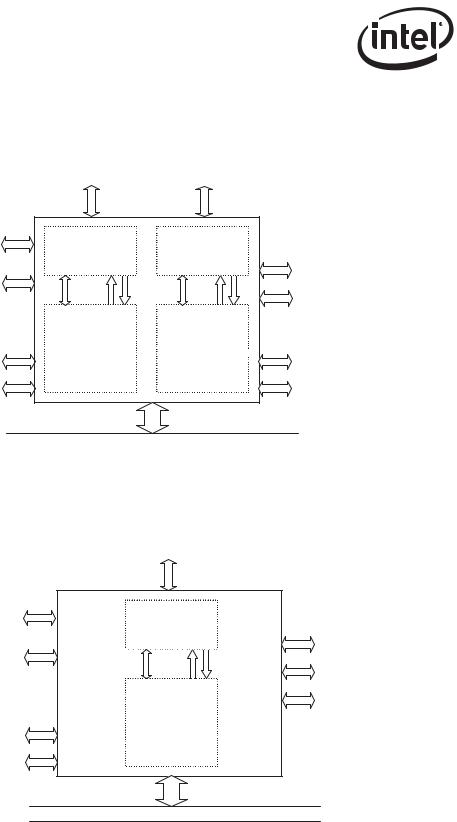
Architectural Overview
2.2External Architecture
Figure 2-1 shows the external interfaces to the 82546GB/EB.
MDI |
MDI |
Interface A |
Interface B |
1000Base-T PHY Interfaces
Design for |
|
10/100/1000 |
|
Test Interface |
|
||
|
PHY |
||
|
|
||
External |
|
GMII/ |
|
TBI Interface |
MDIO |
||
MII |
|||
|
|
||
|
Device |
||
|
Function 0 |
||
LEDs |
MAC/Controller |
||
(LAN A) |
|||
Software |
|
|
|
Defined Pins |
|
|
|
10/100/1000 PHY
MDIO |
GMII/ |
|
MII |
||
|
Device
Function 1
MAC/Controller 
(LAN B)
SMBus
Interface
EEPROM
Interface
 Flash Interface
LEDs
Software
Defined Pins
PCI (64-bit, 33/66 MHz)/PCI-X (133 MHz)
Figure 2-1. 82546GB/EB External Interface
Figure 2-2 shows the external interfaces to the 82545GM/EM, 82544GC/EI, 82540EP/EM, and
82541xx.
MDI
Interface
|
|
1000Base-T PHY Interface |
|
|
Design for |
|
10/100/1000 |
|
|
Test Interface |
|
|
||
|
PHY |
SMBus |
||
|
|
|||
External |
|
|
Interface |
|
|
GMII/ |
|
||
TBI Interface |
MDIO |
EEPROM |
||
MII |
||||
(82545GM/EM only) |
|
|
Interface |
|
|
Device |
Flash Interface |
||
|
|
|||
|
Function 0 |
|
||
LEDs |
MAC/Controller |
|
||
Software |
|
|
|
|
Defined Pins |
|
|
|
|
PCI (64-bit, 33/66 MHz)/PCI-X (133 MHz)
Note: 82540EP/EM and 82541xx do not support PCI-X; 82544GC/EI and 82541ER do not support SMBus interface
Figure 2-2. 82545GM/EM, 82544GC/EI, 82540EP/EM, and 82541xx External Interface
8 |
Software Developer’s Manual |

Architectural Overview
Figure 2-3 shows the external interfaces to the 82547GI/EI.
CSA Port |
PCI Core |
EEPROM |
FLASH |
|
Slave |
DMA Function |
|
|
Access |
|
||
Descriptor Management |
|
||
Logic |
|
||
|
|
||
|
|
40KB |
|
|
|
Packet |
|
|
|
RAM |
|
Control |
TX/RX MAC |
RX Filters |
|
(Perfect, |
|||
Status |
|||
CSMA/CD |
Multicast, |
||
Logic |
|||
|
VLAN) |
||
|
|
||
|
VLA |
|
|
|
N |
|
|
Statistics |
|
|
8 bits
Management
8 bits
Interface
|
Trellis Viterbi |
|
Side-stream |
|
|
|
|
||
|
Encoder/Decoder |
|
Scrambler/ |
|
|
|
|||
|
|
|||
|
|
|
Descrambler |
|
|
|
|
|
|
PHY
4 bits
Control
4 bits
ECHO, NEXT,
FEXT
Cancellers
AGC, A/D
Timing
Recovery
4DPAM5 Encoder
Pulse Shaper,
DAC, Filter
|
Hybrid |
|
|
|
|
Line Driver |
|
|
|
|
|
|
|
|
|||
|
|
|
|
|
|
|
|
|
|
|
|
|
|
|
|
|
|
|
|
|
|
|
|
|
|
|
Media Dependent Interface
Figure 2-3. 82547GI(EI) External Interface
Software Developer’s Manual |
9 |
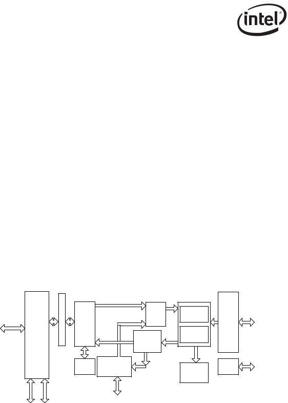
Architectural Overview
2.3Microarchitecture
Compared to its predecessors, the PCI/PCI-X Family of Gigabit Ethernet Controller’s MAC adds improved receive-packet filtering to support SMBus-based manageability, as well as the ability to transmit SMBus-based manageability packets. In addition, an ASF-compliant TCO controller is integrated into the controller’s MAC for reduced-cost basic ASF manageability.
Note: The 82544GC/EI and 82541ER do not support SMBus-based manageability.
For the 82546GB/EB, this new functionality is packaged in an integrated dual-port combination. The architecture includes two instances of both the MAC and PHY along with a single PCI/PCI-X interface. As a result, each of the logical LAN devices appear as a distinct PCI/PCI-X bus device.
The following sections describe the hardware building blocks. Figure 2-4 shows the internal microarchitecture.
2.3.1PCI/PCI-X Core Interface
The PCI/PCI-X core provides a complete glueless interface to a 33/66 MHz, 32/64-bit PCI bus or a 33/66/133 MHz, 32/64 bit PCI-X bus. It is compliant with the PCI Bus Specification Rev 2.2 or 2.3 and the PCI-X Specification Rev. 1.0a. The Ethernet controllers provide 32 or 64 bits of addressing and data, and the complete control interface to operate on a 32-bit or 64-bit PCI or PCI-X bus. In systems with a dedicated bus for the Ethernet controller, this provides sufficient bandwidth to support sustained 1000 Mb/s full-duplex transfer rates. Systems with a shared bus (especially the 32-bit wide interface) might not be able to maintain 1000 Mb/s, but can sustain multiple hundreds of Mbps.
|
Host Arbiter |
|
|
|
|
|
TX |
TX MAC |
|
|
|
(10/100/ |
Link I/F |
|
|
|
Switch |
||
|
DMA |
1000 Mb) |
GMII/ |
|
|
|
|||
|
|
|
MII |
|
PCI/ |
Engine |
|
RX MAC |
|
|
|
|||
|
|
|
||
PCI Interface PCI-X |
|
Packet/ |
(10/100/ |
|
Core |
|
1000 Mb) |
|
|
|
Manageability |
|
||
|
|
Filter |
|
|
|
Packet |
ASF |
|
MDIO |
|
|
MDIO |
||
|
Buffer |
Manageability |
RMON |
|
|
|
|||
|
|
|
Statistics |
|
|
|
SM Bus |
|
|
EEPROM Flash
Figure 2-4. Internal Architecture Block Diagram
10 |
Software Developer’s Manual |

Architectural Overview
When the Ethernet controller serves as a PCI target, it follows the PCI configuration specification, which allows all accesses to it to be automatically mapped into free memory and I/O space at initialization of the PCI system.
When processing transmit and receive frames, the Ethernet controller operates as master on the PCI bus. As a master, transaction burst length on the PCI bus is determined by several factors, including the PCI latency timer expiration, the type of bus transfer being made, the size of the data transfer, and whether the data transfer is initiated by receive or transmit logic.
The PCI/PCI-X bus interfaces to the DMA engine.
2.3.282547GI/EI CSA Interface
CSA is derived from the Intel® Hub Architecture. The 82547EI Controller CSA port consists of 11 data and control signals, two strobes, a 66 MHz clock, and driver compensation resistor connections. The operating details of these signals and the packet data protocol that accompanies them are proprietary. The CSA port has a theoretical bandwidth of 266 MB/s — approximately twice the peak bandwidth of a 32-bit 33 MHz PCI bus.
The CSA port architecture is invisible to both system software and the operating system, allowing conventional PCI-like configuration.
2.3.3DMA Engine and Data FIFO
The DMA engine handles the receive and transmit data and descriptor transfers between the host memory and the on-chip memory.
In the receive path, the DMA engine transfers the data stored in the receive data FIFO buffer to the receive buffer in the host memory, specified by the address in the descriptor. It also fetches and writes back updated receive descriptors to host memory.
In the transmit path, the DMA engine transfers data stored in the host memory buffers to the transmit data FIFO buffer. It also fetches and writes back updated transmit descriptors.
The Ethernet controller data FIFO block consists of a 64 KB (40 KB for the 82547GI/EI) on-chip buffer for receive and transmit operation. The receive and transmit FIFO size can be allocated based on the system requirements. The FIFO provides a temporary buffer storage area for frames as they are received or transmitted by the Ethernet controller.
The DMA engine and the large data FIFOs are optimized to maximize the PCI bus efficiency and reduce processor utilization by:
•Mitigating instantaneous receive bandwidth demands and eliminating transmit underruns by buffering the entire out-going packet prior to transmission
•Queuing transmit frames within the transmit FIFO, allowing back-to-back transmission with the minimum interframe spacing
•Allowing the Ethernet controller to withstand long PCI bus latencies without losing incoming data or corrupting outgoing data
•Allowing the transmit start threshold to be tuned by the transmit FIFO threshold. This adjustment to system performance is based on the available PCI bandwidth, wire speed, and latency considerations
Software Developer’s Manual |
11 |

Architectural Overview
•Offloading the receiving and transmitting IP and TCP/UDP checksums
•Directly retransmitting from the transmit FIFO any transmissions resulting in errors (collision detection, data underrun), thus eliminating the need to re-access this data from host memory
2.3.410/100/1000 Mb/s Receive and Transmit MAC Blocks
The controller’s CSMA/CD unit handles all the IEEE 802.3 receive and transmit MAC functions while interfacing between the DMA and TBI/internal SerDes/MII/GMII interface block. The CSMA/CD unit supports IEEE 802.3 for 10 Mb/s, IEEE 802.3u for 100 Mb/s and IEEE 802.3z and IEEE 802.3ab for 1000 Mb/s.
The Ethernet controller supports half-duplex 10/100 Mb/s MII or 1000 Mb/s GMII mode and all aspects of the above specifications in full-duplex operation. In half-duplex mode, the Ethernet controller supports operation as specified in IEEE 802.3z specification. In the receive path, the Ethernet controller supports carrier extended packets and packets generated during packet bursting operation. The 82554GC/EI, in the transmit path, also supports carrier extended packets and can be configured to transmit in packet burst mode.
The Ethernet controller offers various filtering capabilities that provide better performance and lower processor utilization as follows:
•Provides up to 16 addresses for exact match unicast/multicast address filtering.
•Provides multicast address filtering based on 4096 bit vectors. Promiscuous unicast and promiscuous multicast filtering are supported as well.
•The Ethernet controller strips IEEE 802.1q VLAN tag and filter packets based on their VLAN ID. Up to 4096 VLAN tags are supported1.
In the transmit path, the Ethernet controller supports insertion of VLAN tag information, on a packet-by-packet basis.
The Ethernet controller implements the flow control function as defined in IEEE 802.3x, as well as specific operation of asymmetrical flow control as defined by IEEE 802.3z. The Ethernet controller also provides external pins for controlling the flow control function through external logic.
2.3.5MII/GMII/TBI/Internal SerDes Interface Block
The Ethernet controller provides the following serial interfaces:
•A GMII/MII interface to the internal PHY.
•Internal SerDes interface2 (82546GB/EB and 82545GM/EM)/Ten Bit Interface (TBI)2 for the 82544GC/EI: The Ethernet controller implements the 802.3z PCS function, the AutoNegotiation function and 10-bit data path interface (TBI) for both receive and transmit operations. It is used for 1000BASE-SX, -LX, and -CX configurations, operating only at 1000 Mb/s full-duplex. The on-chip PCS circuitry is only used when the link interface is configured for TBI mode and it is bypassed in internal PHY modes.
1.Not applicable to the 82541ER.
2.Not applicable to the 82544GC/EI, 82540EP/EM, 82541xx, and 82547GI/EI.
12 |
Software Developer’s Manual |

Architectural Overview
Note: Refer to the Extended Device Control Register (bits 23:22) for mode selection (see Section 13.4.6).
The link can be configured by several methods. Software can force the link setting to AutoNegotiation by setting either the MAC in TBI mode (internal SerDes for the 82546GB/EB and 82545GM/EM), or the PHY in internal PHY mode.
The speed of the link in internal PHY mode can be determined by several methods:
•Auto speed detection based on the receive clock signal generated by the PHY.
•Detection of the PHY link speed indication.
•Software forcing the configuration of link speed.
2.3.610/100/1000 Ethernet Transceiver (PHY)
The Ethernet controller provides a full high-performance, integrated transceiver for 10/100/
1000 Mb/s data communication. The physical layer (PHY) blocks are 802.3 compliant and capable of operating in half-duplex or full-duplex modes.
Highlights of the PHY blocks are as follows:
•Data stream serializers and encoders. Encoding techniques include Manchester, 4B/5B and 4D/PAM5. These blocks also perform data scrambling for 100/1000 Mb/s transmission as a technique to minimize radiated Electromagnetic Interference (EMI).
•A multi-mode transmit digital to analog converter, which produces filtered waveforms appropriate for the 10BASE-T, 100BASE-TX or 1000BASE-T Ethernet standards.
•Receiver Analog-to-Digital Converter (ADC). The ADC uses a 125 MHz sampling rate.
•Receiver decoders. These blocks perform the inverse operations of serializers, encoders and scramblers.
•Active hybrid and echo canceller blocks. The active hybrid and echo canceller blocks reduce the echo effect of transmitting and receiving simultaneously on the same analog pairs.
•NEXT canceller. This unit removes high frequency Near End Crosstalk induced among adjacent signal pairs.
•Additional wave shaping and slew rate control circuitry to reduce EMI.
Because the Ethernet controller is IEEE-compliant, the PHY blocks communicate with the MAC blocks through an internal GMII/MII bus operating at clock speeds of 2.5 MHz up to 125 MHz.
The Ethernet controller also uses an IEEE-compliant internal Management Data interface to communicate control and status information to the PHY.
2.3.7EEPROM Interface
The PCI/PCI-X Family of Gigabit Ethernet Controllers provide a four-wire direct interface to a serial EEPROM device such as the 93C46 or compatible for storing product configuration information. Several words of the data stored in the EEPROM are automatically accessed by the Ethernet controller, after reset, to provide pre-boot configuration data to the Ethernet controller before it is accessible by the host software. The remainder of the stored information is accessed by various software modules to report product configuration, serial number and other parameters.
Software Developer’s Manual |
13 |

Architectural Overview
2.3.8FLASH Memory Interface
The Ethernet controller provides an external parallel interface to a FLASH device. Accesses to the FLASH are controlled by the Ethernet controller and are accessible to software as normal PCI reads or writes to the FLASH memory mapping area. The Ethernet controller supports FLASH devices with up to 512 KB of memory.
Note: The 82540EP/EM provides an external interface to a serial FLASH or Boot EEPROM device. See Appendix B for more information.
2.4DMA Addressing
In appropriate systems, all addresses mastered by the Ethernet controller are 64 bits in order to support systems that have larger than 32-bit physical addressing. Providing 64-bit addresses eliminates the need for special segment registers.
Note: The PCI 2.2 or 2.3 Specification requires that any 64-bit address whose upper 32 bits are all 0b appear as a 32-bit address cycle. The Ethernet controller complies with the PCI 2.2 or 2.3 Specification.
PCI is little-endian; however, not all processors in systems using PCI treat memory as little-endian. Network data is fundamentally a byte stream. As a result, it is important that the processor and Ethernet controller agree about the representation of memory data. The default is little-endian mode.
Descriptor accesses are not byte swapped.
The following example illustrates data-byte ordering for little endian. Bytes for a receive packet arrive in the order shown from left to right.
01 02 03 04 05 06 07 08 09 0a 0b 0c 0d 0e 0f 10 11 12 13 14 15 16 17 18 19 1a 1b 1c 1d 1e
Example 2-1. Byte Ordering
There are no alignment restrictions on packet-buffer addresses. The byte address for the major words is shown on the left. The byte numbers and bit numbers for the PCI bus are shown across the top.
Table 2-1. Little Endian Data Ordering
|
|
63 |
|
|
|
|
|
|
0 |
|
|
7 |
6 |
5 |
4 |
3 |
2 |
1 |
0 |
|
|
|
|
|
|
|
|
|
|
Byte |
0 |
08 |
07 |
06 |
05 |
04 |
03 |
02 |
01 |
Address |
|
|
|
|
|
|
|
|
|
8 |
10 |
0f |
0e |
0d |
0c |
0b |
0a |
09 |
|
|
|
|
|
|
|
|
|
|
|
|
10 |
18 |
17 |
16 |
15 |
14 |
13 |
12 |
11 |
|
|
|
|
|
|
|
|
|
|
|
18 |
20 |
1f |
1e |
1d |
1c |
1b |
1a |
19 |
|
|
|
|
|
|
|
|
|
|
14 |
Software Developer’s Manual |

Architectural Overview
2.5Ethernet Addressing
Several registers store Ethernet addresses in the Ethernet controller. Two 32-bit registers make up the address: one is called “high”, and the other is called “low”. For example, the Receive Address Register is comprised of Receive Address High (RAH) and Receive Address Low (RAL). The least significant bit of the least significant byte of the address stored in the register (for example, bit 0 of RAL) is the multicast bit. The LS byte is the first byte to appear on the wire. This notation applies to all address registers, including the flow control registers.
Figure 2-5 shows the bit/byte addressing order comparison between what is on the wire and the values in the unique receive address registers.
Preamble & SFD Destination Address Source Address
...55 |
|
D5 |
|
00 |
AA |
00 |
11 |
22 |
33 |
|
...XXX |
||||
Bit 0 of this byte is first on the wire |
|
|
|
|
|
|
|
dest_addr[0] |
|||||||
|
|
|
|
|
|
|
|
|
|
|
|
|
|
|
|
|
|
|
|
|
|
|
|
|
|
|
|
|
|
|
|
|
|
|
|
|
|
|
33 |
22 |
11 |
00 |
AA |
00 |
|
|
|
Destination |
|
address |
|
|
|
|
|
||||||||
|
stored |
|
|
|
|
|
|
|
|
||||||
internally as shown here |
|
|
|
|
|
|
|
|
Multicast bit |
||||||
|
|
|
|
|
|
|
|
|
|
|
|
|
|
|
|
|
|
|
... |
|
|
|
33 |
22 |
11 |
00 |
AA |
00 |
|
|
|
|
|
|
|
|
|
|
|
|
|
|
|
|
|
|
|
Figure 2-5. Example of Address Byte Ordering
The address byte order numbering shown in Figure 2-5 maps to Table 2-2. Byte #1 is first on the wire.
Table 2-2. Intel® Architecture Byte Ordering
IA Byte # |
1 (LSB) |
2 |
3 |
4 |
5 |
6 (MSB) |
|
|
|
|
|
|
|
Byte Value (Hex) |
00 |
AA |
00 |
11 |
22 |
33 |
|
|
|
|
|
|
|
Note: The notation in this manual follows the convention shown in Table 2-2. For example, the address in Table 2-2 indicates 00_AA_00_11_22_33h, where the first byte (00h_) is the first byte on the wire, with bit 0 of that byte transmitted first.
Software Developer’s Manual |
15 |

Architectural Overview
2.6Interrupts
The Ethernet controller provides a complete set of interrupts that allow for efficient software management. The interrupt structure is designed to accomplish the following:
•Make accesses “thread-safe” by using ‘set’ and ‘clear-on-read’ rather than ‘read-modify-write’ operations.
•Minimize the number of interrupts needed relative to work accomplished.
•Minimize the processing overhead associated with each interrupt.
Intel accomplished the first goal by an interrupt logic consisting of four interrupt registers. More detail about these registers is given in sections 13.4.17 through 13.4.21.
•Interrupt Cause ‘Set’ and ‘Read’ Registers
The Read register records the cause of the interrupt. All bits set at the time of the read are autocleared. The cause bit is set for each bit written as a 1b in the Set register. If there is a race between hardware setting a cause and software clearing an interrupt, the bit remains set. No race condition exists on writing the Set register. A ‘set’ provides for software posting of an interrupt. A ‘read’ is auto-cleared to avoid expensive write operations. Most systems have write buffering, which minimizes overhead, but typically requires a read operation to guarantee that the write operation has been flushed from the posted buffers. Without autoclear, the cost of clearing an interrupt can be as high as two reads and one write.
•Interrupt Mask ‘Set’ (Read) and ‘Clear’ Registers
Interrupts appear on PCI only if the interrupt cause bit is a 1b, and the corresponding interrupt mask bit is a 1b. Software can block assertion of the interrupt wire by clearing the bit in the mask register. The cause bit stores the interrupt event regardless of the state of the mask bit. The Clear and Set operations make this register more “thread-safe” by avoiding a ‘read- modify-write’ operation on the mask register. The mask bit is set to a 1b for each bit written in the Set register, and cleared for each bit written in the Clear register. Reading the Set register returns the current value.
Intel accomplished the second goal (minimizing interrupts) by three actions:
•Reducing the frequency of all interrupts (see Section 13.4.17). Not applicable to the
82544GC/EI.
•Accepting multiple receive packets before signaling an interrupt (see Section 3.2.3)
•Eliminating (or at least reducing) the need for interrupts on transmit (see Section 3.2.7)
The third goal is accomplished by having one interrupt register consolidate all interrupt information. This eliminates the need for multiple accesses.
Note that the Ethernet controller also supports Message Signaled Interrupts as defined in the PCI 2.2, 2.3, and PCI-X specifications. See Section 4.1.3.1 for details.
16 |
Software Developer’s Manual |
Loading...