

Page 1
SERVICE MANUAL
DTR-7.6
Ref. No. 3914
SERVICE MANUAL
7
Q
Q
TEL 13942296513 QQ 376315150 892498299
3
6
3
1
5
1
5
0
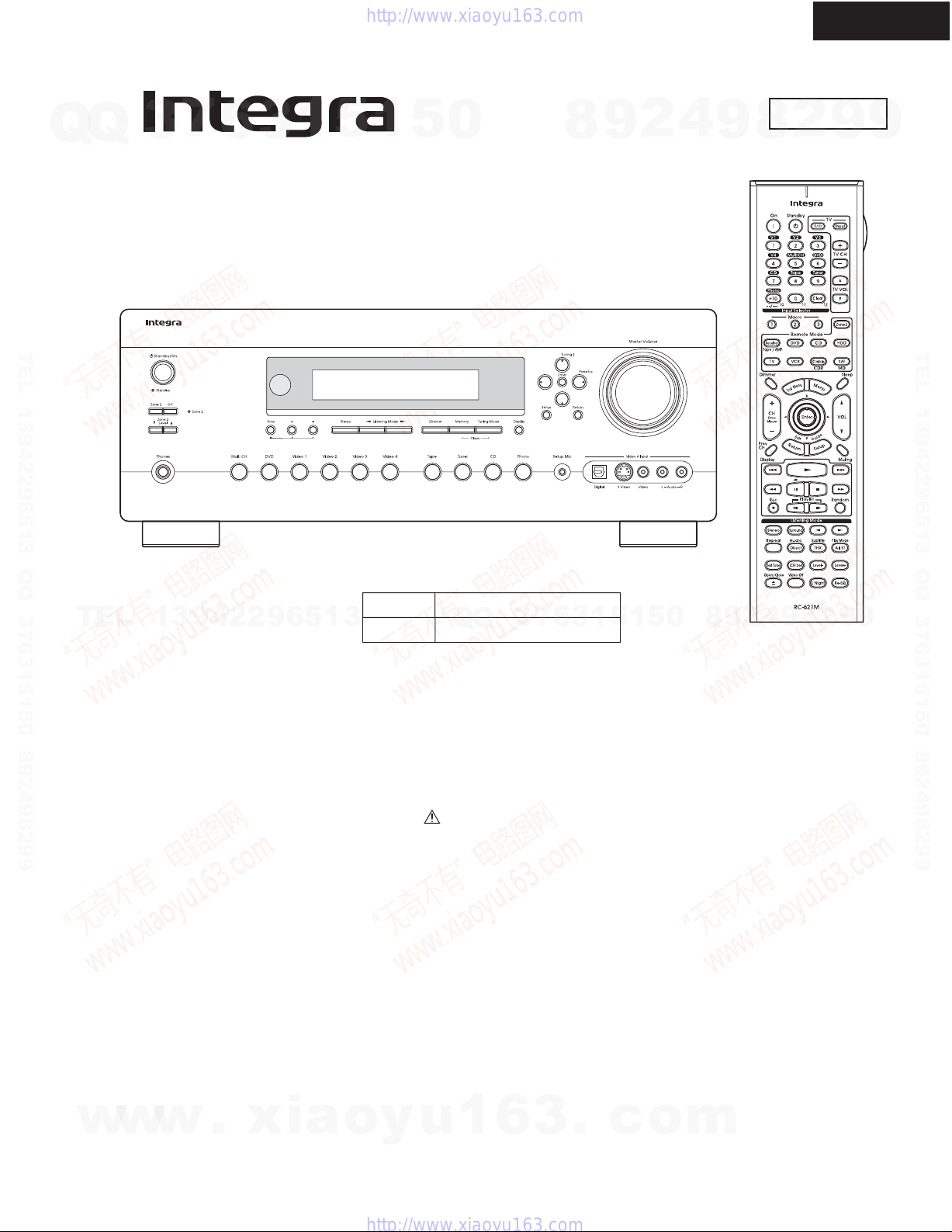
AV RECEIVER
MODEL DTR-7.6
8
9
2
4
DTR-7.6
9
Nov., 2005
2
8
9
9
TEL 13942296513 QQ 376315150 892498299
TEL
13942296513
Black model
120V AC, 60HzBMDD
Q
BMPA
SAFETY-RELATED COMPONENT
WARNING!!
THE MARK FOUND ON SOME COMPONENT
PARTS INDICATES THE CRITICAL FOR RISK OF
FIRE AND ELECTRIC SHOCK.
WHEN REPLACING, BE SURE TO USE PARTS OF
IDENTICAL DESIGNATION.
MAKE LEAKAGE-CURRENT OR RESISTANCE
MEASUREMENTS TO DETERMINE THAT EXPOSED
PARTS ARE ACCEPTABLY INSULATED FROM THE
SUPPLY CIRCUIT BEFORE RETURNING THE
APPLIANCE TO THE CUSTOMER.
Q
230V~240V AC, 50Hz
3
7
6
3
1
5
1
5
0
8
9
2
9
4
RC-621M
8
2
9
9
w
w
w
.
xia
o
y
u
1
6
3
.
c
o
m
Page 2
Q
IC BLOCK DIAGRAMS AND DESCRIPTIONS
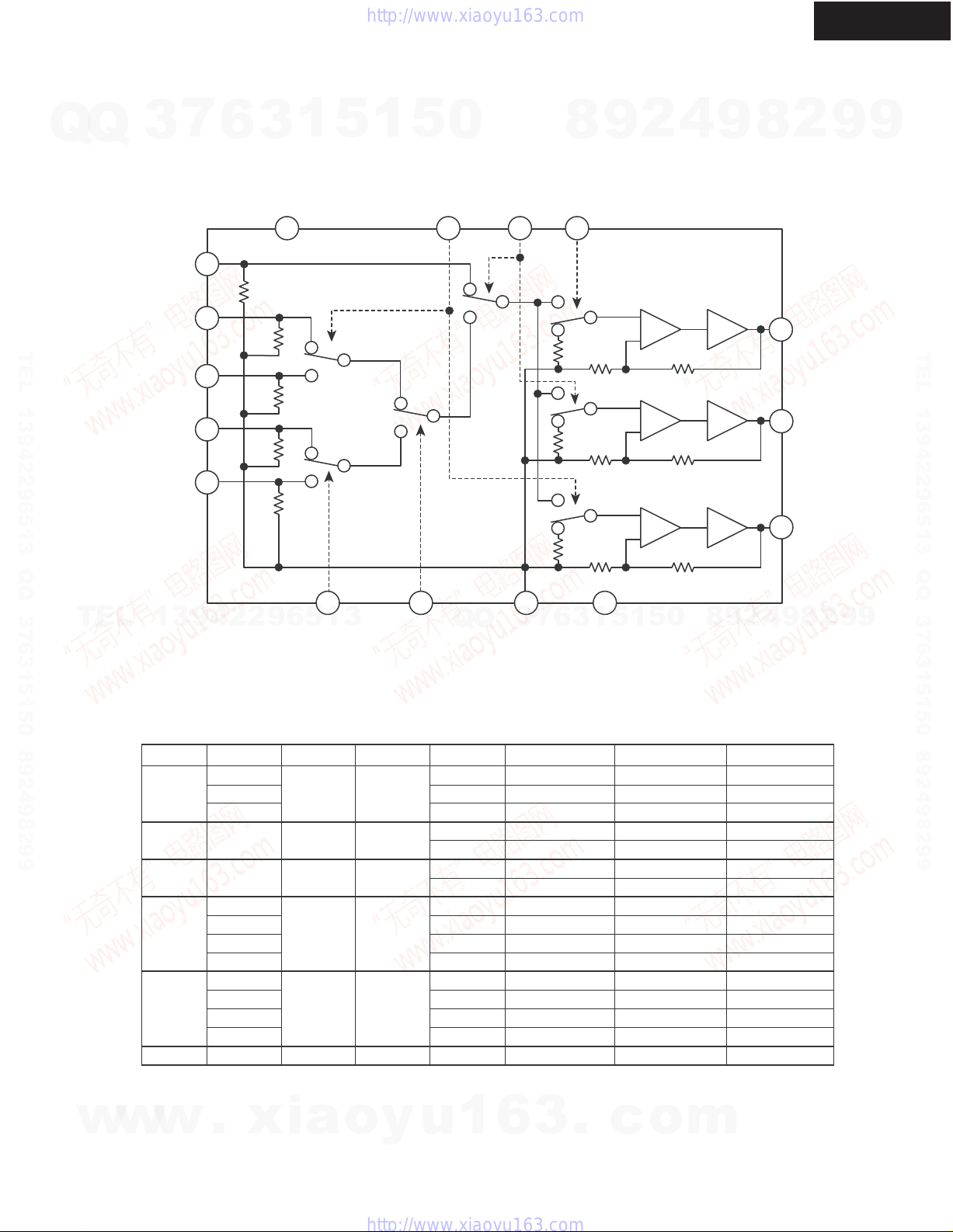
NJM2595M(5-INPUT 3-OUTPUT VIDEO SWITCH)
7
Q
3
BLOCK DIAGRAM
6
3
1
5
1
5
0
8
9
2
4
9
8
DTR-7.6
2
9
9
SW2 SW1V+
1016 214
13
Vin1
Vin2
TEL 13942296513 QQ 376315150 892498299
Vin3
Vin4
Vin5
TEL
13942296513
9
20k
7
20k
5
20k
3
20k
S2
S4
S3
Q
Q
S1
3
7
SW5
20k
20k
20k
6
3
S5
S6
S7
1
V-SW3 SW4 GND
6dB
Amp
6dB
Amp
6dB
Amp
81264
5
1
5
0
75ohms
Driver
75ohms
Driver
75ohms
Driver
8
9
2
4
1
15
11
9
Vout1
Vout2
Vout3
2
8
9
TEL 13942296513 QQ 376315150 892498299
9
w
w
TRUTH TABLE
Control Signal vs. Output Signal (L=VCL, H=VCH, X=L or H)
L
H
H
H
H
L
w
H
L
H
L
H
H
H
L
L
H
H
L
L
L
.
xia
SW4SW3SW2SW1
XX
X
X
L
H
X
o
L
L
H
H
X
y
u
SW5
H
H
L
H
L
H
L
H
L
H
L
H
L
H
L
L
1
6
Vout1
Vin1
Vin1
MUTE
Vin2
MUTE
Vin3
MUTE
Vin4
MUTE
Vin4
MUTE
Vin5
MUTE
Vin5
MUTE
MUTE
3
.
c
Vout2
MUTE
MUTE
MUTE
Vin2
Vin2
Vin3
Vin3
Vin4
Vin4
Vin4
Vin4
Vin5
Vin5
Vin5
Vin5
MUTE
o
Vout3
Vin1
MUTE
Vin1
MUTE
MUTE
Vin3
Vin3
Vin4
Vin4
MUTE
MUTE
Vin5
Vin5
MUTE
MUTE
MUTE
m
Page 3

DTR-7.6
A
PRINTED CIRCUIT BOARD VIEW
POWER AMPLIFIER
SECTION
Q
1
TEL 13942296513 QQ 376315150 892498299
2
Q
3
7
BCDEFGH
U06
6
3
NAAF-8678,Power amplifier PC board
1
5
1
5
0
8
9
2
4
9
8
2
9
U064
NAAF-8682,
Surround back
amplifier PC board
U061
9
TEL 13942296513 QQ 376315150 892498299
NAPS-8679,
Power transformer
terminal PC board
3
4
T
E
L
1
3
9
4
2
2
9
6
5
1
3
Q
Q
3
7
6
3
1
5
1
5
0
8
9
2
4
9
8
2
9
9
U062
5
w
w
w
.
x
i
a
o
y
u
1
6
3
.
c
o
m
NAETC-8680,
Thermal detector
PC board
Page 4
DTR-7.6
A
BCDEFGH
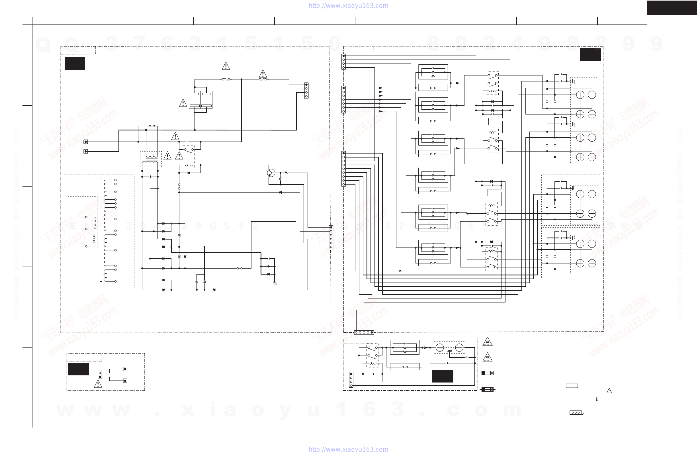
SCHEMATIC DIAGRAM 7
POWER SUPPLY SECTION
3
1
Q
Q
NAPS-8664
U04
NOTE: <D>: US model only
<A>: Australian model only
TEL 13942296513 QQ 376315150 892498299
AC-H
1
2
3
T
4
P906A
P907A
T901
NPT-1526D <D>
NPT-1526P <A>
3
E
L
2
TO NAPS-8664
1
AC-G
1
NPT-1519JQ <D>
NPT-1519GQ <A>
1
7
T902
S1+
S1H+
GND
S1H-
S1S2+
GND
3
S2-
TO NAPS-8665 P951TO NAPS-8665 P952
S3+
GND
S3S4+
S4-
6
J901
T902
234
1
678
9
5
C902
223J
TO NAAF-8678 JL6952B
1SS133
4
D905
D906
D908
D909
D901
1SS133
D902
1SS133
D903
1SS133
D904
1SS133
1SS133
1SS133
1SS133
2
9
P910
103M/275
C912
4
RL902
3 2
J905
2
+
2200/35
C903
+
100/50
C904
3
3
1
1
D912
1SS133
9
D907
1SS133
100K
R909
C906
1
F903
2.5A-SE-EAK <A>
5A-UL/T-233 <D>
4
2
6
+
3.3/50
D910
DZ-6.8BSC <D>
DZ5.6BSB <A>
5
1
J907
5
3
1
C991
D991
D992
1
F901
6.3A-SE-EAK <A>
10A-UL/T-233 <D>
Q912
2SC1740
R913
1K
R914
100K
D913
1SS133
222J
1SS133
1SS133
P991
5
1
3
+12VTRG
2
P91
APOWER
+10S
POFF1
RLGND
DGND
0
1
2
3
4
5
6
NAETC-8666
1
+22VR
CSRLD
2
CSP
3
CSPE
4
TO NAETC-8667
JL6602B
LSP
1
RSP
2
CSP
3
SLSP
4
SRSP
5
SBLSP
6
SRBSP
7
TO NAAF-8678
JL6600B
JL6603B
LSPE
1
RSPE
2
CSPE
3
SLSPE
4
SRSPE
5
SBLSPE
6
SBRSPE
7
RLGND
8
+22V
9
Q
Q
JL911A
3
R6690
7
0.22
(1/2W)
6
8
<A>
L6600
S1.3C
R6600
22
R6610
22
<D>
J6600
<A>
S1.3C
L6601
R6601
22
R6611
22
<D>
J6604
<A>
L6603
S1.3C
R6603
22
R6613
22
<D>
J6619
<A>
L6604
S1.3C
R6604
22
R6614
22
<D>
J6620
<A>
L6605
S1.3C
R6605
22
22
R6615
<D>
J6626
3
<A>
L6606 S1.3C
R6606
22
R6616
22
<D>
J6625
1
9
5
1
2
5
2
6
RL6600
D6600
C6600
103Z
C6603
RL6603
6
2
5
C6605
6
2
5 4
RL6605
5
D6607
C6607
6
2
5
RL6607
D6605
103Z
4
3
1
D6603
103Z
4
1
3
0
103Z
1
3
4
4
9
8
2
9
9
U043
*
C6650
102J
C6651
103J
C6640
C6641
*
*
C6653
102J
102J
1
3
9
8
C6654
*
103J
C6644
C6656
C6655
102J
*
103J
103J
C6645
2
C6658
C6657
102J
*
103J
103J
C6647
*: Australian model only
102J
103J
*
C6643
*
*
C6646
102J
C6648
103J
102J
*
*
*
*
10
*
*
4
*
5
1
2
3
4
6
7
8
9
5
4
2
3
1
5
4
2
3
1
P6607
P6600
L
SL
SB SPEAKER
P6605
SBL
9
Z2 SPEAKER
Z2L
R
SR
SBR
Z2R
8
2
9
TEL 13942296513 QQ 376315150 892498299
9
RLGND
Z2RLD
SBRLD
CSRLD
FRLD
12345
JL2006B
TO NAVD-8657
AC120V~60Hz <D>
AC220-230V~50/60Hz <A>
NAETC-8671
U048
5
INLET
w
w
P908
2
1
1
1
w
P906B
P907B
AC-HAC-G
TO NAPS-8664
.
x
i
a
o
y
u
NAETC-8667
TO NAETC-8666
1
JL6602A
1
2
3
4
5
2
1
RL6602
C6602
103Z
6
L6602 S1.3C
R6602
4
3
6
R6612
J6851
<A>
<D>
22
22
1
C
5
P6602
C6642 *
103J
3
C6652
102J
*
U044
3
.
c
o
CAUTION
FOR CONTINUED PROTECTION
AGAINST FIRE HAZARD, REPLACE
ONLY WITH FUSE OF SAME TYPE
AV
AND RATING INDICATED.
ATTENTIION
AFIN D'ASSURER UNE PROTECTION
PERMANENTE CONTRE LES RISQUES
D'INCENDIE, REMPLACER UNIQUEMENT
AV
PAR UN FUSIBLE DE MEME TYPE
ET CALIBRATION COMME INDIQUE.
THIS SYMBOL LOCATED NEAR THE FUSE INDICATES
THAT THE FUSE USED IS SLOW OPERATING TYPE
FOR CONTINUED PROTECTION AGAINST FIRE FUSE
HAZARD,REPLACE WITH SAME TYPE FUSE. FOR FUSE
RATING REFER TO THE MAKING ADJACENT TO THE SYMBOL.
CE SYMBOLE INDIQUE QUE LE FUSIBLE UTLISE EST
A LENT, E POUR UNE PROTECTION PERMANENTE,N'UTILISER
QUE DES FUSIBLES DE MEME TYPE. CE DARNIER EST
INDIQUE LA QU LE PRESENT SYMBOL EST APPOSE.
m
NOTE
REPLACE ONLY WITH PART NUMBER SPECIFIED.
ELECTROLYTIC CAPACITORS ARE IN
ALL CAPACITORS ARE IN pF/50WV UNLESS OTHERWISE NOTED.
EX) 030 3pF 330 33pF 331 330pF 333 0.033uF
ALL RESISTORS ARE IN OHMS 1/4WATTS UNLESS OTHERWISE NOTED.
THE THICK LINES ON PC BOARD ARE THE PRINTING SIDE OF THE PARTS
EX PRINTING SIDE
CIRCUIT IS SUBJECT TO CHANGE FOR IMPROVEMENT.
ARE CRITICAL FOR SAFETY.THE COMPONENTS IDENTIFIED BY MARK
+
uF/WV.
Page 5
SPECIFICATIONS
DTR-7.6
Q
Q
TEL 13942296513 QQ 376315150 892498299
TEL
Amplifier Section
Power Output
2 channels driven:
Dynamic Power
THD (Total Harmonic
Distortion) 0.08% (Power Rated)
Damping Factor 60 (Front, 1 kHz, 8 )
Input Sensitivity and
Impedance 200 mV/ 47 k (LINE)
Output Level and
Impedance 200 mV/ 470 (REC OUT)
Phono Overload 70 mV (MM 1 kHz, 0.5%)
Frequency Response 5 Hz~100 kHz/ +1 dB-3 dB (LINE)
Tone Control ±10 dB, 50 Hz (BASS)
Signal to Noise Ratio 106 dB (LINE, IHF-A)
Speaker Impedance 4 ~ or 6 ~
Video Section
Input Sensitivity/Output
Level and Impedance 1 Vp-p /75 (Component and S-Video Y)
Component Video
Frequency Response 5 Hz ~ 100 MHz
Tuner Section
FM
Tuning Frequency Range
Usable Sensitivity Stereo: 22.2 dBf (75 IHF)
Signal to Noise Ratio Stereo: 67 dB (IHF-A)
THD Stereo: 0.5% (1 kHz)
Frequency Response 30 Hz~15 kHz / ±1 dB
Stereo Separation 40 dB (1 kHz)
AM
Tuning Frequency Range
Usable Sensitivity 300 µV/m
Signal to Noise Ratio 40 dB
THD 0.70%
3
7
6
1
3
105 W + 105 W (8 , 20 Hz~20 kHz, FTC)
140 W + 140 W (6 , 1 kHz, DIN)
170 W + 170 W (6 , 1 kHz, JEITA)
240 W + 240 W (3 , Front)
180 W + 180 W (4 , Front)
125 W + 125 W (8 , Front)
2.5 mV/47 k (PHONO MM)
±10 dB, 20 kHz (TREBLE)
80 dB (PHONO, IHF-A)
0.7 Vp-p /75 (Component Pb/Cb,Pr/Cr)
0.28 Vp-p /75 (S-Video C)
1 Vp-p /75 (Composite)
13942296513
North American: 87.5 MHz~107.9 MHz
Australian: 87.5 MHz~ 108.0 MHz
Mono: 15.2 dBf (75 IHF)
Mono: 73 dB (IHF-A)
Mono:0.3% (1 kHz)
North American: 530 kHz~1710 kHz
Australian: 522/530 kHz~1611/1710 kHz
5
1
5
0
Q
General
Power Supply North American: AC 120 V, 60 Hz
Power Consumption North American: 7.5 A
Standby Power
Consumption North American: 0.1 W
Dimensions
(W
Weight North American: 13.1 kg
Video Inputs
HDMI IN1, IN2
Component IN1, IN2, IN3
S-Video DVD, VIDEO1, VIDEO2, VIDEO3,
Composite DVD, VIDEO1, VIDEO2, VIDEO3,
Video Outputs
HDMI OUT
Component OUT
S-Video MONITOR OUT, VIDEO1, VIDEO2
Composite MONITOR OUT, VIDEO1, VIDEO2
Audio Inputs
Digital Inputs Optical: 5 (1 on Front Panel)
3
Q
Analog Inputs DVD (MULTICHANNEL), VIDEO1,
Multichannel Input 7.1 ch (DVD)
Audio Outputs
Digital Output Optical: 1
Analog Outputs TAPE, VIDEO1, VIDEO2, ZONE2
Multichannel Pre
Outputs 7.1 ch
Speaker Outputs L, R, C, SL, SR, SBL, SBR
Phones 1
RS232 1
IR Input/Output 2/1
12 V Trigger Out
Specifications and features are subject to change without
notice.
8
× H × D)
3
6
7
1
4
2
9
Australian: AC 230-240 V, 50 Hz
Australian: 680 W
Australian: 0.5 W
435 × 173.5 × 428.5 mm
17-1/8" × 6-13/16" × 16-7/8"
Australian: 13.3 kg
VIDEO4
VIDEO4
8
0
5
1
5
Coaxial: 2
VIDEO2, VIDEO3, VIDEO4, TAPE, CD,
PHONO
L/R/SUBWOOFER
ZONE2 (L, R)
A, B, C
9
28.9 lbs.
29.3 lbs.
2
9
8
4
2
9
8
2
9
9
9
TEL 13942296513 QQ 376315150 892498299
9
w
w
w
.
xia
o
y
u
1
6
3
.
c
o
m
Page 6
SERVICE PROCEDURES
TX-SR803/E
DTR-7.6
7
Q
Q
TEL 13942296513 QQ 376315150 892498299
TEL
3
1. Replacing the fuses
This symbol located near the fuses indicates that the
fuse used is fast operating type. For continued protection against
fire hazard, replace with same type fuse. For fuse rating refer to
the marking adjacent to the symbol.
Ce symbole indique que le fusible utlise est a rapide.
Pour une protection permanente, n'untiliser que fusibles de
meme type. Ce darnier est la qu le present symbol est
appse.
CIRCUIT NO. PART NO. DESCRIPTION
F6901,F6902 252301GR 12A-TUL-250V,Fuse
F901 252079GR 6.3A-SE-EAK,Fuse <A>
F903 252075GR 2.5A-SE-EAK,Fuse <A>
F931,F932 252073GR 1.6A-SE-EAK,Fuse
F951,F952 252079GR 6.3A-SE-EAK,Fuse
2. To initialize the unit
This device employs a microprocessor to perform various
functions and operations. If interference generated by an external
power supply, radio wave, or other electrical source results in
13942296513
accident which causes the specified operations and functions to
operate abnormally.
To perform a result, please follow the procedure below.
1.Press and hold down the VIDEO-1 button, then press the
STANDBY button.
2.After "Clear" is displayed, the preset memory and each
mode stored in the memory, such as surround, are
initialized and will return to the factory setting.
6
252330GR 10A-UL/T-233,Fuse <D>
252326GR 5A-UL/T-233,Fuse <D>
Note: <D>:120V model only
<A>: Australian model only
3
1
5
1
5
0
Q
Q
3
7
8
6
3
1
9
5
2
1
5
0
4
9
8
9
2
8
4
2
9
8
2
9
9
9
TEL 13942296513 QQ 376315150 892498299
9
3. Safety-check out
(U.S.A. model only)
After correcting the original service problem, perform the
following safety check before releasing the set to the customer.
Leakage Current Check
Measure leakage current to a known earth ground(water pipe,
conduit, etc.) by connecting a leakage current tester between
the earth ground and exposed metal parts of the appliance
(input/output terminals, screwheads,metal overlays, etc.).
4. Changing the AM band step
With the exception of the worldwide models, a tuning step selector
switch is not provided. When you change the band step, change
the parts as shown below.
To 10kHz To 9kHz
R714 Open 10 k
w
w
w
.
xia
o
y
u
1
6
3
.
c
o
m
Page 7
DTR-7.6
A
EXPLODED VIEW
A401
3
U08
7
Q
1
TEL 13942296513 QQ 376315150 892498299
2
3
4
T
Q
E
L
D model
3
A405
1
BCDEFGH
9
F901
6
A404
A403
U048
4
A051
A105
x 2 pcs.
A062
x 4 pcs.
F903
A402
x 44 pcs.
2
A056
x 4 pcs.
3
A408
x 3 pcs.
A057
x 2 pcs.
U044
2
A065
x 3 pcs.
A110
9
1
F952
F951
U042
U11
U043
F6901
6
A067
A060
A063
5
A082
x 12 pcs.
P691
5
F931
F932
P701
U02
F6902
1
A059
3
Q6050a
x 12 sheets
A105
x 2 pcs.
1
A077
5
U01
U03
U045
U032
A105
x 3 pcs.
U06
0
A105
x 3 pcs.
A090
A082
x 2 pcs.
U064
A105
x 3 pcs.
U062
U063
A083
Q
A081
A080
Q
A080
A083
A105
x 2 pcs.
Q6050a
x 2 sheets
A087
x 2 pcs.
A105
x 4 pcs.
3
7
A089
Q6052Q6054
6
A003
8
Q6062Q6064Q6056
Q6061Q6063Q6066Q6065
Q6050
Q6051Q6053Q6055
1
3
A003
x 11 pcs.
9
Q6060
A420
P7534
5
A012
x 2 pcs.
A020
U07
1
2
0
5
A003
x 3 pcs.
U076
U072
4
A101
x 4 pcs.
8
U077
9
A012
9
A003
A095
A096
2
A003
x 2 pcs.
8
A100
x 4 pcs.
4
U075
A020
A001
9
A005
2
A099
A409
x 3 pcs.
2
8
A410
9
9
A044
x 4 pcs.
9
TEL 13942296513 QQ 376315150 892498299
9
3
U073
.
A003
x 2 pcs.
A015
c
A002
o
U04
5
w
w
w
.
T901
x
A055
x 9 pcs.
i
a
A106
o
x 2 pcs.
y
A052
A054
x 3 pcs.
A053
x 3 pcs.
u
1
A050
A119
x 4 pcs.
A111
x 4 pcs.
A114
x 4 pcs.
6
A008
A003
x 6 pcs.
m
A010
A009
A011
x 2 pcs.
A019
A040
A037
x 3 pcs.
Page 8
DTR-7.6
A
BLOCK DIAGRAM
AMPLIFIER
SECTION
Q
Q
North American models
3
ANTENNA UNIT
XM-RADIO
XM/DT IC
7
1
MIC
VIDEO4 IN
PHONO
CD
TEL 13942296513 QQ 376315150 892498299
TAPE OUT
2
TAPE IN
VIDEO3 IN
VIDEO2 OUT
VIDEO2 IN
VIDEO1 OUT
3
T
E
L
1
VIDEO1 IN
3
BCDEFGH
Micro
MIC AMP
MICDET
Q3001
RIAA
9
Controller
DAC
AK4384
4
6
2
TUNER PACK
3
51
52
53
54
55
56
57
58
59
60
61
62
63
64
65
66
67
68
69
70
71
72
73
2
9
74
6
1
5
41
43
27
29
28
30
21
23
25
22
24
26
1
TAPE_OUT_L
TAPE_OUT_R
5
Q3003
NJW1157
Z2_L
Z2_R
3
V1_OUT_R
V2_OUT_L
V2_OUT_R
V1_OUT_L
+
+
12
19
11
20
10
21
9
22
8
23
1
42
44
-6dB
Q3002
NJU7311AM
SOURCE_L
SOURCE_R
46
45
48
47
4
27
3
28
2
29
7
24
5
26
6
25
5
Q3004
ADLT+
ADLT-
ADRT+
MIX_L
MIX_R
-6dB Inv.
VOLIN_
SBL
VOLIN_
SBR
ADRT-
+9.7dB
DAC_FR
DAC_FL
0
DAC_SW
DAC_SL
DAC_CT
DAC_SR
DAC_SBL
MCH_CT
MCH_SW
DAC_SBR
Q
MCH_SL
MCH_SR
MCH_SBL
MCH_SBR
Q
FRL
9
CSRL
SBRL
2
Z2RL
8
9
SPEAKER TERMINALS
9
2
9
FRONT LEFT
FRONT RIGHT
CENTER
SURR. LEFT
TEL 13942296513 QQ 376315150 892498299
SURR. RIGHT
SUUR. BACK
LEFT
SUUR. BACK
RIGHT
ZONE2 LEFT
ZONE2 RIGHT
9
4
HEADPHONES
PREOUT
SPRLSB
ZONE2 PREOUT/LINEOUT
Z2L_PO
Z2R_PO
Z2SW_PO
0
8
9
POWER AMPLIFIER
FL
FR
C
SW
SL
SR
SBL
SBR
L
R
SW
9
2
8
+29dB
+29dB
+29dB
+29dB
+29dB
+29dB
+29dB
4
1
2
SPRLF
5
1
2
3
Q3007
+20.2dB
8
4
5
6
7
1
HPMUT
AMUT
SBMUT
5
9
Z2LMUT
8
80
88
81
89
82
90
A
87
95
A
83
91
84
92
85
93
86
94
Q3009
BD3814
19
A
TONE
17
A
3
TONE
7
TONE
TONE
+6dB@ZONE2
27
28
3
6
DVD
MC/MSW
Q331,341,351
MSL/MSR
4
5
w
MSBL/MSBR
w
IN1
IN2
OPT FRNT
OPT1
OPT2
OPT3
OPT4
COAX 1
COAX 2
w
OPT OUT
HDMI
Micro
Controller
HDMI
CS5340
RX
SPDIF
.
2ch ADC
2ch ADC
2ch ADC
Q141,Q161
TC74VHT157F
TC74VHT157F
Q211
FLASH ROM
MX29LV040
4M Bit
Q285
SD_RAM
IC4
2S16100
2M Byte
x
i
818280798685127
CS494003
a
MCLK
BCLK
LRCLK
Q201
DSP
RX0
RX1
RX4
RX6
RX5
RX3
RX2
RX7
TX
59
131
119
134
111
117
107
106
109
110
118
o
ADLT-
ADLT+
61
54
2ch ADC
2
3
1
64
63
62
56
y
DIR
ADRT+
161413
15
ADRT-
60
49
48
43
47
46
45
44
42
50
+6dB
VLSC
LPF
303132
u
VLSC
LPF
+6dB
33
1
+6dB
VLSC
LPF
36
37
Q361
CS42518/CS42528
6
VLSC
LPF
35
+6dB
34
8ch DAC
VLSC
LPF
28
+6dB
292627
3
VLSC
LPF
+6dB
.
VLSC
LPF
22
+6dB
23
+6dB
VLSC
LPF
21
20
c
o
m
12V TRIGGER
CONTROL
IR REMOTE
SENSOR
INTERFACE
RS232C
INTERFACE
From/to
MICROPROCESSOR
RI
12V TRIGGER A
12V TRIGGER B
12V TRIGGER C
IR IN A
IR IN B
IR OUT
RIex
RS232C
Page 9
DTR-7.6
A
BCDEFGH
BLOCK DIAGRAM VIDEO SECTION
Q
1
TEL 13942296513 QQ 376315150 892498299
2
Q
COMPONENT VIDEO INPUT
Y1
CB1
CR1
Y2
CB2
CR2
Y3
CB3
3
7
6
3
1
5
1
5
0
A
8
9
B
2
4
9
8
2
COMPONENT VIDEO OUTPUT
9
Y
CB
9
TEL 13942296513 QQ 376315150 892498299
CR3
RL2201~
7
6dB
RL2203
6
6dB
LA7106M
Q2107
Q2106
LA7106M
.
1
3
6dB
SDET*{OSD+(OSD*SI)}
6dB
SDET*{OSD+(OSD*SI)}
6dB
c
5
RL2204,
RL2205
1
SDET*{OSD+(OSD*SI)}
0
5
SDET*{OSD+(OSD*SI)}
SDET*OSD
SDET*OSD
o
m
8
9
2
4
9
2
8
COMPOSITE VIDEO OUTPUT
Q2004
3
4
5
T
E
COMPOSITE VIDEO INPUT
DVD
VIDEO1
VIDEO2
VIDEO3
VIDEO4
(FRONT)
S VIDEO INPUT
DVD
VIDEO1
VIDEO2
VIDEO3
VIDEO4
(FRONT)
w
L
C
YC
YC
C
Y
YC
w
1
3
Q2001
NJM2595
Y
Q2002
NJM2595
Y
Q2003
NJM2595
C
w
SDET*{OSD+(OSD*SI)}
9
4
6dB
6dB
6dB
6dB
6dB
6dB
6dB
6dB
6dB
.
2
2
SDET*{OSD+(OSD*SI)}
x
9
6
OSD
LC74763-9836
i
5
a
0dB
1
3
-6dB
-6dB
-6dB
-6dB
o
0dB
AIN1
AIN2
AIN3
AIN4
AIN5
y
Q2101
ADV7183A
Y1
COMPOSITE
/ Y2
COMPOSITE
C1
C2
u
DIGITAL VIDEO DECODER
OSD*(SDET+SI)
SDET*OSD
Q
DIGITAL VIDEO ENCODER
1
Q
Q2104
ADV7172
DACA
DACB
DACC
DACD
DACE
DACF
CB
CR
6
3
6dB
Y
V
Y
C
3
CR
9
9
MONITOR
VIDEO1
VIDEO2
C
Y
MONITOR
CY
VIDEO1
C
Y
VIDEO2
S VIDEO OUTPUT
Page 10
DTR-7.6
A
SCHEMATIC
DIAGRAM 1
Q
VIDEO
SECTION
1
TEL 13942296513 QQ 376315150 892498299
2
3
4
T
Q
E
NAVD-8657
3
CR
(PR)
CB
(PB)
Y
P2201 COMPONENT 3
C2202
102K
CR
(PR)
CB
(PB)
Y
P2201 COMPONENT 2
CR
(PR)
CB
(PB)
Y
P2201 COMPONENT 1
CR
(PR)
CB
(PB)
Y
C2201
102K
P2202 COMPONENT OUT
P2001
DEO
C
VIDEO3
C
OUT
IN
L
VIDEO2
P2002
CY
C
OUT
C
VIDEO1
IN
C
P2003
DVD
CY
P2007
MONITOR
7
R2207
R2209
V
V
1
V
V
V
V
V
75
R2019
C2016
470J
C2010
470J
75
R2007
R2004 75
10K
R2001
C2001
102K
75
R2020
C2017
757575
R2013
R2014
C2003
102K
C2011
75
R2008
C2002
102K
75
R2005
10K
R2002
C2021
C2020
75
C2019
R2021
470J
3
R2015
470J
75
R2009
75
R2006
10K
R2003
R2018
R2016
C2018
470J
C2009
C2008
C2007
C2006
C2005
C2004
R2017
C2015
C2014
C2013
R2012
R2011
R2010
C2012
470J
Y
Y
Y
Y
Y
BCDEFGH
R2201
R2208
104Z
10/50
10/50
104Z
10/50
10/50
C-MON
Y-MON
V-MON
75
75
75
104Z
10/50
10/50
75
75
75
104Z
10/50
10/50
0
0
0
V3
V3
V3
V2COUT
V2YOUT
9
V1COUT
V1YOUT
C
Y
V2OUT
V2C
V1OUT
V2Y
V2
V1C
V1Y
DVDC
DVDY
DVD
6
.7M
4
4.7M
R2202
4
2
V1
75
330
R2087
R2088
3
Y
CB
CR
RL2201
4.7M
R2203
104Z
C2030
-
RL2202
-
RL2203
-
D2201
1SS352
Q2201
2SC2712-GR
R2204
16151413121110
V+
100/16
Vout2
Q2003 NJM2595M
Vout1
SW5
C2031
1234567
Selector & 6dB AMP
2
16151413121110
V+
C2026 104Z
104Z
C2022
100/16
C2027
100/16
C2023
SW1
Vout2
Q2002 NJM2595M
Vout1
SW5
1234567
16151413121110
V+
SW1
Vout2
Q2001 NJM2595M
Vout1
SW5
1234567
+
+
+
Q2202
2SC2712-GR
1K
Vin1
SW1
Vin5
SW3
9
Vin1
Vin5
SW3
Vin1
Vin5
SW3
5
w
w
w
.
x
GND
GND
Vin4
Vin4
GND
Vin4
R- S3
R2092
470
R2093
R-S5
R2097
470
R2098
R-S 4
Vout3
SW4
6
Vout3
SW4
Vout3
SW4
R2089
R2090
2.2
R-S7
82
82
i
1
RL2204
-
RL2205
-
D2202
1SS352
R2205
R-S1
SW2
Vin3
SW2
Vin3
SW2
Vin3
8.2
R-S8
+
+
R-S2
1K
9
Vin2
V8
5
9
Vin2
V8
9
Vin2
V8
Q2012
RN1443
Q2013
RN1443
Q2017
RN1443
Q2018
RN1443
Q2020
RN1443
a
P2004
V4Y
V4C
V4V
GNDV
FSWSTB
47K
R2056
R2055
R2053
6.8K
C2056
820K
R2050
C2050
470J
Q2010
RN2402
R2062
IO
G
104Z
C2107
C2112
10/16
104Z
6
C2119
VIDEO+5V
2.7K
L2001
056J
1K
C2057
1/50
682J
220
33K
104Z
C2116
C2122
C2118
10/16
C2063
0.47/50
R2064
C2136
C2105
104Z
104Z
C2111
104Z
104Z
VIDEO-5V
334J
C2061
C2058
223J
C2055
122K
C2052
104Z
C2051
470/10
R2063
2.2K
C2106
104Z
C2121
102K
C2108
104Z
C2109
104Z
68
C2067
104Z
470/10
102
-12 VA
L2103
220K
J
C2059
220J
0
C2060
270J
6.8K
R2048
R2049
D2002
1SS352
D2003
1SS352
Q2009
2SA1162-GR
103K
C2135
AIN7
41
42
43
44
45
46
47
48
49
50
51
52
53
54
55
56
57
58
59
60
OSDSDO
OSDCLK
FSWSDO
OSDCS
FSWCLKVCL
5
100/16
104Z
C2032
C2033
1
3
104Z
100/16
C2028
C2029
104Z
100/6.3
C2024
C2025
C2073
470/10
R2091
10K
R2094
10K
120
R2096
R2095
120
C2078
470/10
Q2024
RN1443
Q2023
RN1443
o
R-S5
R-S6
C2091
10/50
C2092
10/50
C2041
100D
C2042
180J
Except 120V model
C2043
17.73MHZ
180J
C2044
080D
C2045
470J
C2046
470J
C2047
470J
C2048
470J
Q2008
2SA1162-GR
Q2102
BA33BC0FB
IO
C2101
104Z
Q2025
RN1443
R-S6
1
C2090
104Z
OSD
X2001
14.32MHZ
X2002
R2041
2.2K
R2042
2.2K
R2043
2.2K
R2044
2.2K
C2049
1/50
220
R2058
220
R2066
G
C2102
470/10
Q2004
LC74763-9836
Vss1
XTALIN1
2
XTALOUT1
3
HSYNCOUT
4
XTALIN2
5
XTALOUT2
6
VSYNCOUT
7
OSDCS
8
OSDDATA
9
OSDSCK
10
11
SW1
12
SW2
13
SW3
14
SW4
15 16
RST
220
R2059
220
R2067
Q2022
2SA1162-GR
R2101
1K
R2103
1K
R2105
1K
L2101
220K
R2107
1K
y
VCOOUT
AMPOUT
SYNCIN
R2060
R2061
C2110
C2103
C2104
10/16
Vd
CDET
N
VCOIN
AMPIN
PDOUT
Vss
SEPC
CVCR
CVIN
Vdd2
CVOUT
12K
2.7K
30
d1
29
28
27
26
FC
25
24
23
22
21
20
19
18
17
C2065
100/16
104Z
C2115
10/16
103K
5
L2007
022K
R2057
D2001
1SS352
R2054
120
R2052
1.5K
R2051
C2054
0.33/50
C2066
104Z
Q2103
BA18BC0FB
C2137
R2102
1K
R2104
1K
R2106
1K
C2113
104Z
C2114
C2117
10/1
C2120
104Z
R2108
1K
u
P2005
GND
+12VA
L2002
022K
Q2005
2SC1712-GR
C2053
100/16
1K
R2046
47K
3.3K
R2045
R2047
Q2007
RN1443
104Z
C2068
Q
R2065
L2104
022K
C2132
823J
C2133
103J
680
R2116
104Z
1K
R2114
R2115
C2134
39
38
35
40
36
N
NC
AGND
AGND
ELPF 37
PVDD
PWRD
AIN1
AIN8
AIN2
AIN9
AIN3
AGND
CAPY1
CAPY2
AVDD
REFOUT
CML
AGND
CAPC1
CAPC2
AGND
AIN10
AIN4
AIN11
AIN5
NC
NC
AIN662
ALSB66
RESET
63
65
AIN12
61
64
C2125
104Z
100
R2109
Video Decoder
1
SYNC
SDET
PLLSDA
VSYNC
U02
Q2006
RN1443
10K
R-S5
Q
10K
DVDD
104Z
C2130
4.7K
C2129
34
33P132
P0
NC
ADV7183B
NC
SCLK68
SDA67
697071
100
103K
C2124
R2112
R2111 100
VMUT
PLLSCL
VCSRST
R-S6
C2131
103K
080D
X2101
27MHZ
29
30
31
28
XTAL
DVDD
DGN D
XTAL1
Q2101
DVDD
DGNDNC
P15
72
73
C2126
104Z
6
SPRLZ2
C2128
080D
LLC1 27
P1474
SPRLSB
SPRLCS
LLC2 26
P1375
SPRLF
25
24P323P422P521
P2
NC
NC
P1276
77
L-S4
3
DVDDIO
DVDDIO
NC
78
L-S3
L-S2
R2071
R2072
R2073
R2074
L-S5
R2075
L-S6
R2076
L-S7
R2077
R2078
L-S8
P6
P7
NC
NC
NC
DGND
NC
SFL
NC
DVDD
DGND
P8
P9
P10
P11
DGND
HS
VS
OE
FIELD
80
79
3
L-S1
20
19
18
17
16
15
14
13
12
11
10
9
8
7
6
5
4
3
2
1
C2072
104Z
100K
100K
100K
100K
100K
100K
100K
100K
7
JL2006
RLGND
FRLD
CSRLD
SBRLD
Z2RLD
Q2052
Q2051
RN1401
RN1401
C2071
104Z
22
R2070
1
2
3
4
5
6
7
8
9
Q2111 NJU7313AM
10
11
12
13
14
STB
GND
15 16
6
Switch Controller
C2186
104Z
C2185
104Z
C2123
104Z
DVDDIO
L2102
R2129
220K
.
8
DATA
CLK
3
33
Q2053
RN1401
30
29
28
27
26
25
24
23
22
21
20
19
18
17
SPEAKER
RELAY DRIVER
9
Q2054
RN1401
R-S1
R-S2
R2083
100K
R2082
100K
R-S3
R2086
100K
R-S4
R2085
100K
R2081
R-S5
100K
R2080
R-S6
100K
R
-S7
R2079
100K
R
-S8
R2084
100K
5
1
PLLSCL
Q2109
2SK3019
2
R2113
2.2K
PLLSDA
Q2108
2SK3019
R2110
2.2K
VCSRST
Q2105
RN1401
R2145
R2121
R2122
R2123
R2124
R2125
R2126
R2127
R2128
L2105
022K
4.7K
R2143
100
VAA1
33
P02
33
P13
33
P24
33
P35
33
P46
33
P57
33
P68
33
P79
CSO
C2188
VAA
11
12
104Z
GN
D
R2133
100
R2132
100
C2164
10/16
c
1
Video Encoder
C2189
C2163
33
104Z
104Z
R2144
464748
45
VSO
GND
VAA
CLOCK
ADV7172
IELD
O10
_HS
F
C/
VSYN
HSYNC
BLANK
GND
16
14
15
13
K
4.7
R2131
o
2
5
44
42
RESET
CLAMP
PAL_NTSC 43
Q2104
ALSB17
VAA
GND
18
19
4.7K
R2130
41
TTX
SCLOCK20
R2134
C2141
R2141
40
TXREQ
DATA
S
21
1.2K
104Z
1.2K
R2135
0
1.2K
R2142
37
39
COMP1
RSET1 38
DACA35
ESET/RTC
VAA
DACB
SCR
VAA
GND
VAA
DACC 29
CD 28
DA
VAA
GND
DA
RSET222
COMP 223
DACF24
C2142
1.2K
104Z
4
104Z
C2161
VREF
C2162
36
104Z
34
33
32
31
30
27
26
25
CE
m
8
R2186
R2185
R2184
R2183
R2182
R2181
R2187
VIDEO+5V
VIDEO-5V
C2176
105K
82
R2192
C2175
105K
82
R2191
C2174
105K
82
68
C2173
105K
82
R2189
C2172
105K
82
R2188
C2171
82
105K
68
68
68
R2190
68
68
9
2
9
Video AMP with HPF
VMUT
R2172
100K
R2171
100
R2170
100K
R2169
100
R2168
100K
R2167
100
R2166
100K
R2165
100
R2164
100K
R2163
100
R2162
R2161
100
100K
C2184
C2183
Q2107
LA7106M
8
NFB3
7
VIN3+
6
-VCCI
5
NFB2
4
VIN2+
3
MODE1
2
NFB1
1
VIN1+
C2179
8
NFB3
7
VIN3+
6
-VCCI
5
NFB2
4
VIN2+
3
MODE1
2
NFB1
1
VIN1+
Q2106
LA7106M
8
4
100/16
104Z
-VCC2
MODE2
VOUT3
DRCTL
VOUT2
VOUT1
+VCC
C2180
100/16
104Z
-VCC2
MODE2
VOUT3
DRCTL
VOUT2
GND
VOUT1
+VCC
GND
2
9
9
TEL 13942296513 QQ 376315150 892498299
9
9
2
8
9
9
10
11
12
13
C2182
14
104Z
15
16
C2181
100/16
9
10
11
12
13
C2178
104Z
14
15
16
C2177
100/16
R2178
82
R2177
82
R2176
R2180
390
R2174
100
R2179
390
R2173
100
CR
82
CB
R2175
18
Y
Page 11
DTR-7.6
A
BCDEFGH
SCHEMATIC
DIAGRAM 2
Q
DSP SECTION
1
TEL 13942296513 QQ 376315150 892498299
2
3
4
5
Q
T
E
w
DIGITAL OUT
L
w
COAX1
P101
COAX2
OPT1
DIGITAL IN
OPT2
OPT3
OPT4
P102
3
2
1
3
4
U101
IN
VCC
GND
U102 1
IN
VCC
GND
U103 1
IN
VCC
GND
U104
IN
VCC
GND
U105
IN
VCC
GND
DACSBR
DACSBL
1
DACSR
DACSL
DACSW
DACC
DACFR
DACFL
w
5
1
3
2
3
2
3
2
1
3
2
3
2
1
L101
022K
L102
022K
R125
330
R111
220
104Z
R112
220
104Z
R113
220
104Z
R114
220
104Z
R115
220
104Z
SYSIN
C125
102K
C146
102K
75
75
C111
C112
C113
C114
C115
7
NE5532ASPR
1
7
NE5532ASPR
1
7
NE5532ASPR
1
7
NE5532ASPR
1
R101
R102
+
C116
Q433:A
Q433:B
3
Q432:A
Q432:B
Q431:A
Q431:B
Q430:A
Q430:B
7
101J
C101
101J
C102
100/16
NE5532ASPR
8
4
NE5532ASPR
8
4
NE5532ASPR
8
4
NJM4580M-D
8
4
6
R103
C103
104K
10
R105
220K
220K
R106
R104
C104
104K
10
L122
470M
Q121
R526
22K
6
R536
1.5K
7
Q423:A
5
1.5K
R546
1.5K
R545
3
1
Q423:B
2
R535
1.5K
R525
9
22K
R524
22K
6
R534
1.5K
7
Q422:A
5
R544
1.5K
1.5K
R543
3
1
Q422:B
2
1.5K
R533
NE5532ASPR
22K
R523
R527
22K
6
R537
1.5K
7
Q421:A
5
R547
1.5K
1.5K
R542
3
1
Q421:B
2
R532
1.5K
NE5532ASPR
22K
R522
R521
22K
6
R531
1.5K
7
Q420:A
5
R541
1.5K
1.5K
3
R540
1
Q420:B
2
1.5K
R530
NE5532ASPR
22K
R520
10K
R108
080D
C106
9
10
8
IN4
OUT5
OUT4
GND
TC74HCU04AF
7
65432
NE5532ASPR
8
R496
6
22K
5
4
22K
R506
R516
22K
R505
R515
3
22K
2
R495
4
NE5532ASPR
NE5532ASPR
8
R494
6
22K
5
4
22K
R504
R514
22K
R513
R503
3
22K
2
R493
NE5532ASPR
8
R497
6
22K
5
4
22K
R517
R507
22K
R502
R512
3
22K
2
R492
NJM4580M-D
8
R491
6
22K
5
4
22K
R511
R501
22K
R510
3
22K
2
R490
.
R500
080D
11
IN5
22K
22K
22K
22K
22K
22K
22K
22K
10K
C105
12
OUT6
080D
R486
1.5K
C446
471J
C445
471J
1.5K
R485
R484
1.5K
C444
471J
C443
471J
1.5K
R483
R487
1.5K
C447
471J
C442
471J
1.5K
R482
R481
1.5K
C441
471J
C440
471J
1.5K
R480
R107
13
IN6
C107
NE5532ASPR
NE5532ASPR
NE5532ASPR
NE5532ASPR
NE5532ASPR
NE5532ASPR
NJM4580M-D
GNDA
P3101B
L121
470M
VCC
114
10K
R109
C108
104K
220K
R110
R476
10K
7
1
2
10K
R474
10K
7
1
10K
R473
R477
10K
7
1
10K
R472
R471
10K
7
NE5532ASPR
1
R470
10K
GNDA
GNDA
100/16
+
C121
C122 104Z
8
Q413:A
4
Q413:B
R475
8
Q412:A
4
Q412:B
8
Q411:A
4
Q411:B
8
Q410:A
4
Q410:B
ADRT-
ADLT-
ADRT+
TO NAAF-8678
R466
6
10K
5
C436
122J
C435
122J
3
10K
2
R465
2
R464
6
10K
5
C434
122J
C433
122J
3
10K
2
R463
R467
6
10K
5
C437
122J
C432
122J
3
10K
2
R462
R461
6
10K
5
C431
122J
C430
122J
3
10K
2
R460
DACSBL
DACSBR
x
ADLT+
3
OPT1
COAX1
OPT2
OPT3
OPT4
TX
COAX2
DACSR
DACFR
DACSL
DACFL
9
DACSW
HDMISPF
NE5532ASPR
NE5532ASPR
NE5532ASPR
NE5532ASPR
NE5532ASPR
NE5532ASPR
NE5532ASPR
NE5532ASPR
220/25
DACC
151413121110987654321
C555
7
1
7
1
7
1
7
1
+15VVLSC
Q403:A
6
Q403:B
Q402:A
Q402:B
Q401:A
Q401:B
Q400:A
Q400:B
C556
220/25
i
1
NADG-8660
R436
C426
8
4
C416
C415
8
4
8
4
8
4
R456
121K
180
6
C406
470J
5
R446
180
121K
R445
121K
5
180
3
C405
470J
2
C425
R455
180
121K
C424
R454
121K
180
6
C404
471J
5
R444
121K
180
C413 R423
R443
121K
180
3
C403
471J
2
R453
121K
180
C423
C427
R457
153J
3.3K
6
C407
333J
5
R447
153J
180
C412 R422
R442
121K
180
3
C402
471J
2
121K
R452
180
C422
C421
R451
121K
180
6
C401
471J
5
R441
121K
180
C410 R420
R440
121K
180
3
C400
471J
2
121K
R450
180
C420
R555
15(1/2W)
R556
15(1/2W)
10K
R426
R425
R435
10K
R434
10K
R424C414
R433
R437
10K
R427C417
R432
10K
R431
10K
R421C411
R430
a
U03
R586
R416
3.3K
680
R406
R576
680
3.3K
10K
10K
R575
1
R405
680
3.3K
R585
R415
3.3K
680
R414
R584
680
3.3K
R404
R574
680
3.3K
10K
10K
R573
R403
680
3.3K
R413
R583
680
3.3K
10K
R587
R417
3.3K
680
R407
R577
680
3.3K
470
10K
10K
R402
R572
680
3.3K
R582
R412
680
3.3K
R411
R581
680
3.3K
R571
R401
680
3.3K
10K
10K
R570
R400
680
3.3K
R580
R410
680
3.3K
10K
R557
R558
5
ADRTADRT+
ADLT+
ADLT-
SBR-
SBR+
3
SBL+
SBL-
SR-
SR+
SL+
SL-
FR-
FR+
FL+
FL-
22(1/2W)
22(1/2W)
o
+15VADC
220/25
C558
220/25
-15VADC-15VVLSC
TO NAVD-8655
1011121314151617181920
1
C365
47/25(RFS)
+
C366
17
104Z
18
+
C367
19
100/16
20
21
22
23
C368
24
104Z
25
26
27
28
29
30
31
32
C369
+
220/6.3
L363
022M
SWSW+
C+
C-
C557
y
5
0
C131
104Z
R135
TC7WU04FU
Q131
8
1
VD
2
7
3
6
L133
5
4
GND
LM182
R131
1M
2 1
X131
HC-49U0
120J
312.288MHz
C395
222J
R396
3.9K
DIGSDO
DIRCS
220
R366 220
R365
10
9
INT1
CS/AD0
R371
2.7K
473K
C371
C379 330J
C378
C377 330J
C376
C375
C374
C373 330J
DIGSDI
R364 220
8
CDIN/AD1
CDOUT/SAD
64:CX_SDIN2
63:CX_SDIN3
62:CX_SDIN4
C372
330J
330J
330J
330J
DIGCLK
220
R363
7
6
CCLK/SCL
50:TXP
49:RXP0
104Z
330
R372
COAX2
OPT2
120J
C133
104Z
C363
R36247
104Z
C362
5
4
3
VD1
VLC
DGND1
SAI_SDOUT
330
R373 330
R374 330
R375
OPT3
OPT1
OPT4
C132
R394 56
R391 56
R39356R392 56
C396
222J
R395
3.9K
DIRINT
DIRRST
R367 220
R368 220
11
13
15
12
16
14
AINL-
_RST
AINR-
AINL+
VQ
AINR+
FLT+
REFGND
AOUTB4AOUTB4+
AOUTA4+
AOUTA4-
Q361
VA
AGND1
CS42528-CQ
AOUTB3AOUTB3+
AOUTA3+
AOUTB2+:31
AOUTA3-
AOUTA2+:32
AOUTB2-
AOUTA2-34AOUTB1-35AOUTB1+36AOUTA1+37AOUTA1-38MUTEC39LPFLT40AGND241VARX42RXP7/GP743RXP6/GP644RXP5/GP545RXP4/GP446RXP3/GP347RXP2/GP248RXP1/GP1
33
222K
C370
u
0
PCMLRCK
PCMBCK
022M
L362
R36147
LM182
2
1
CX_SCLK
CX_LRCK
CX_SDIN1
SAI_SLCK
SAI_LRCK
OMCK
ADCIN1
ADCIN2
CX_SDOUT
RMCK
DGND2
330
R377 330
R376
COAX1
L131
VLS
VD2
PCMLR
R133
680
+
R378
PCMSBLR
PCMCSW
PCMSLR
L361
47
64
47
63
47
62
61
47
60
47
59
58
57
47
56
55
47
54
53
52
51
R380
50
R379
49
C381
022M
L364
C380
220/6.3
330
1
RXMUTE
ADCMCK
022M
C361
+
Q
220/6.3
R387
R386
R385
L367
R384
R383
R382
L366 LM182
R381
C384
104Z
330
330
330J
OPTF
HDMISPF
TXMUTE
R175
0
VSYSRST
MCK_HDMI
R148
R147
OMCK
LM182
HDMISPF
TX
LM182
L142
VD_SCK
R150 0
R149
47
VD_SI
VD_SO
TC74VHC157FT
47
47
Q
C383
104Z
C382
+
220/6.3
L365
022M
+5VHD
VD_STB
+10S
C141
1
SELECT
2
1A
3
1B
4
1Y
5
2A
6
2B
7
2Y
8
GND
R304
10K
C301
10/50
R302
2
6
P801A
GNDV
+5VHD
104Z
VCC
C303
222J
R305
R303
1.5K
1.2K
1
NE5532ASPR
Q301:B
3
C302
R291
100K
330
R301
MCT
1
TO NAAF-8678
C304
10/50
123456789
GNDV
Q141
ST
4A
4B
4Y
3A
3B
3Y
R264
2.7K
10K
101J
MSW
16
15
14
13
12
11
10
9
022M
DACDA2
DACDA1
DACBCK
ADSDO
SRCLRCK
C214
122J
R263
330
DSPCLKIN
SRCDO
SRCBCK
DSPCS
DIGSDO
DIGSDI
DSPBUSY
DIGCLK
DSPRST
R310
10K
R308
1.5K
C306
101J
R292
100K
C30810/50
MSL
MSR
P3102B
+2.5VDSP
022M
L201
C307
222J
4
10/50
10/50
MSBL
R146
R145
R144
R143
R142
R141
L202
+PLLVDD
680J
C215
3
R309
10K
7
NE5532ASPR
Q301:A
5
+12VA
MSBR
330
47
47
330
47
47
C211
100/16
-2.5VDSP
+
47
47
47
10K
10K
10K
47
47
47
10K
10K
+
47
10K
10K
47
C217
47
330
330
10K
330
330
330
3.3K
220
ADCCT
ADCSW
C305
10/50
R307
1.2K
8
6
330
R306
C314
C318
-12VA
8765432
3
R252
R253
R254
C212
104Z
R256
R257
R258
R259
R260
R261
R262
C213
2.2/16
C216
104Z
R265
R266
R267
R268
104Z
R269
R270
R271
R272
R273
R274
R275
R276
R277
R255
C218
ADCBCK
ADCLRCK
DACDA4
DACDA3
+
C210
100/16
R251
109
110
111
112
113
114
115
116
HDATA0,GPIO0
117
CMPREQ,FLRCLKN2
118
CMPDAT,FSDATAN2
119
FLRCLKN1
120
WR,DS,GPIO10
121
RD,R/W,GPIO11
122
PLLVSS
123
FILT2
124
FILT1
125
PLLVDD
126
XTALO
127
CLKIN,XTALI
128
CLKSEL
129
CS,GPIO9
130
A0,GPIO13
131
FSDATAN1
132
VDD4
133
7
VSS4
134
FSCLKN1,STCCLK2
135
_SCS
136
SCDIN
137
VSS5
138
VDD5
139
A1,GPIO12
140
141
142
143
144
101J
R208
3.3K
R203
C313 222J
R314
10K
C311
10/50
R312
1.2K
1
Q302:B
2
330
R311
8
MLTSEL
1
R161
47
47
330
47
330
330
R246
R247
R248
47
10K
10K
105
104
103
SCLK0
HDATA4,GPIO4
HDATA3,GPIO3
330
10K
R205
R204 330
R206
DIGCLK
DIGSDO
C317
222J
R320
10K
R318
1.5K
NE5532ASPR
4
5
C316
101J
R294
100K
10/50
R162
R163
R164
R165
R166
R245
C209
10K
102
AUDATA4,GPIO28
109:
140:
R207 47
DIGSDI
ADCSL
ADCSR
R319
10K
C315
10/50
7
Q302:A
R316
2
3
4
5
6
7
R244
47
104Z
99
100
101
VSS2
VDD2
MCLK
AUDATA1
AUDATA0
CMPCLK,FSCLKN2
HDATA2,GPIO2
VSS3
VDD3
HDATA1,GPIO1
SCDOUT,SCDIO
3
HINBSY,GPIO8
SCCLK
UHS,_CS_OUT,GPIO17
_RESET
GPIO219FDAT710VDD611VSS612FHS0,_FWR,_FDS
8
10K
10K
R210
R209
R317
1.2K
8
6
330
C324
ADCSLR
R24947
47
R250 47
107
106
108
LRCLK0
AUDATA2
AUDATA3,XMT958A
6
UHS0,GPIO182UHS1,GPOI193_INTREQ4FA1,FSCDIN5GPOI206FA0,FSCCLK7FSCDIO,FSCDOUT
1
3.3K
R202
R201 3.3K
3.3K
DSPINT
R315
10K
R313
1.5K
NE5532ASPR
3
C312
101J
101J 101J
R293
100K
.
9
ADCCSW
ADCSBLR
R172
R171
R170
R169
R168
R167
R23947
88
87
NC289NC1
VDD1
LRCLK1
SD_ADDR10,EXTA10
SD_ADDR4,EXTA4
SD_ADDR5,EXTA5
L161
L141
0
R180
R23847
R23747
83
85
86
SCLKN,GPIO22
LRCLKN,GPIO23
SD_BA,EXTA19
VDDSD1
VSSSD1
_SD_CS
NC484NC3
C161 104Z
SELECT
1A
1B
1Y
2A
2B
2Y
R242
R243
47
10K
97
98
SCLK1
HDATA5,GPIO5
Q161TC74VHC157FT
VCC
ST
4A
4B
4Y
3A
3B
3Y8GND
R24110K
R240
10K
96
93
94
95
HDATA7,GPIO7
HDATA6,GPIO6
AUDATA5,GPIO29
Q201
16
15
47
14
47
13
330
12
47
11
47
10
330
9
C208
104Z
91
92
90
VSS1
AUDATA6,GPIO30
AUDATA7,XMT958B,GPIO31
CS494003
1
5
1
FSH1,_FRD,FR/_W
FDAT615_FCS16_FINTREQ17FDBCK18FDAT519FDAT420VDD721VSS722FDAT323FDBDA24FDAT225DBDA26DBCK27FDAT128TEST29FDAT030_NV_WE,GPIO16
13
14
330
10K
3.3K
C201 104Z
R211 3.3K
R213
R212
R278
DSPFCS
R324
10K
C321
10/50
1.2K
R322
1
NE5532ASPR
2
10/50
C328
C323
Q303:B
R321
DSPFINT
3
330
10K
10K
R218
R217
R216 3.3K
3.3K
R215
47
R214
222J C327 222J
R330
R325
10K
10K
R323
R328
1.5K
1.5K
C322
C326
101J
101J
R296
R295
100K
100K
SD_DATA6,EXTD6
SD_DATA5,EXTD5
SD_DATA4,EXTD4
SD_DATA3,EXTD3
C202 104Z
R219 10K
R329
10K
10/50
7
NE5532ASPR
4
Q303:A
5
R326
R220 3.3K
ADCSBL
ADCSBR
C325
R327
6
330
SD_DQM0
10K
R221
1.2K
8
VDDSD4
VSSSD4
3.3K
R222
3.3K
R223
c
022M
022M
47
R233 47
R235 47
R23647R234
79
80
81
82
SDATAN3,GPIO27
SDATAN2,GPIO26
SDATAN1,GPIO25
SDATAN0,GPIO24
SD_ADAT8,EXTA11
:66
SD_DATA9,EXTA11
SD_DATA10,EXTA13
SD_DATA11,EXTA14
SD_DATA12,EXTA15
SD_DATA13,EXTA16
SD_DATA14,EXTA17
:43
SD_DATA15,EXTA18
10K
10K
BT_WE
R225
R224
o
2
10K
A1A0RASA3A2
R231
R232
CAS
10K
74
75
76
77
73
72
71
70
_SD_RAS78_SD_CAS
69
68
67
SD_ADDR0,EXTA0
SD_ADDR1,EXTA1
SD_ADDR2,EXTA2
SD_ADDR3,EXTA3
66
65
SD_ADDR6,EXTA6
64
SD_CLK_EN
63
SD_ADDR7,EXTA7
62
SD_ADDR8,EXTA8
61
SD_CLK_IN
60
SD_ADDR9,EXTA9
59
SD_CLK_OUT
58
VDDSD2
57
VSSSD2
56
55
54
53
52
51
VDDSD3
50
VSSSD3
49
48
0
5
NC5
47
46
45
SD_DQM1
44
SD_DATA7,EXTD7
43
42
41
40
39
38
37
_NV_OE,GPIO1532_NV_CS,GPIO1433_SD_WE34SD_DATA0,EXTD0
SD_DATA1,EXTD1
SD_DATA2,EXTD2
31
35
36
R226
10K
D2D0SD_WE
BT_CS
BT_OE
D1
R337
C334
10/50
104Z
C335
C339
104Z
R347
C344
10/50
104Z
C345
C349
104Z
R357
100/16
C354
104Z
C355
C359
104Z
L203
022M
+3.3DSPIO
10K
R230
10K
R229
BA/EA19
SD_CS
SD_CKE
R281
0
SD_CKO
C205
L204
104Z
SD8/EA11
SD9/EA12
SD10/EA13
SD11/EA14
SD12/EA15
C204
104Z
SD13/EA16
SA14/EA17
SA15/EA18
SD_UDQM
C203
104Z
SD_LDQM
10K
10K
R227
R228
L332
022M
330
C337
C336
100/16
104Z
+
+
+
C338
100/16
L342
022M
330
C347
C346
100/16
104Z
+
+
+
C348
100/16
L352
022M
330
C357
C356
100/16
104Z
+
+
+
C358
100/16
m
4
C207
100/16
+
A10
C206
104Z
A4
A5
A6
A7
A8
A9
D7
D6
D5
D4
D3
R336
9
RST
10
AINL
11
VQ
12
AINR
13
VA
14
REF_GND
15
FILT+
16
M11M0
CS5340-CZZ
Q331
R346
9
RST
10
AINL
11
VQ
12
AINR
13
VA
14
REF_GND
15
FILT+
16
M11M0
CS5340-CZZ
Q341
R356
9
RST
10
AINL
11
VQ
12
AINR
13
VA
14
REF_GND
15
FILT+
16
M11M0
CS5340-CZZ
Q351
8
5.6
LRCK
SCLK
SDOUT
MCLK
5.6
LRCK
SCLK
SDOUT
MCLK
5.6
LRCK
SCLK
SDOUT
MCLK
9
8
2
Q551
LM2940
3
1
O
I
G
R551
2
0.47(1/2W)
+
+
C552
100/16
C551
9
10/50
9
TEL 13942296513 QQ 376315150 892498299
L285
L281
022M
+VBOOT
A4
A5
A6
A7
SD9/EA12
SD12/EA15
SD13/EA16
SA15/EA18
BT_WE
SA14/EA17
SD11/EA14
SD10/EA13
A8
A9
SD8/EA11
+VSD
GND2
DQ15
DQ14
GNDQ4
DQ13
DQ12
VCCQ4
DQ11
DQ10
GNDQ3
4
or IC42S16100
M12L1616A-7TG
VCCQ3
UDQM
Q285
GND1
ADCLRCK
ADCBCK
ADCCSW
ADCMCK
ADCSLR
ADCSBLR
ADCRST
022M
RXMUTE
9
L192
4.7M
1
C195
TXMUTE
VSYSRST
VD_SCK
VD_SI
VD_SO
VD_STB
+10S
GNDV
GNDV
+9V
+9V
ADCRST
SYSIN
DIRRST
DIRINT
DIRCS
OPTF
DIGSDI
DIGCLK
DSPCS
DSPBUSY
DSPRST
DSPINT
+5VDAC
DSPFCS
DSPFINT
MLTSEL
DIGSDO
+5VDSP
GNDD
GNDD
0.47(1/2W)
R193
1000/16
1
2
3
4
5
6
7
8
9
10
11
12
1
2
3
4
5
6
7
8
9
9
10
11
12
13
14
15
16
17
18
19
20
P601A
TO NAAR-8661
P602A
TO NAAR-8661
Q211
MX26LV040-70
50
49
SA15/EA18
48
SA14/EA17
47
46
SD13/EA16
SD12/EA15
45
104Z
C291
44
43
SD11/EA14
SD10/EA13
42
41
40
SD9/EA12
9
DQ9
SD8/EA11
39
DQ8
C290
104Z
38
37
NC2
SD_UDQM
36
R285
35
SD_CKO
CLK
47
SD_CKE
34
CKE
33
NC1
32
A9
A9
A8
31
A8
30
A7
A7
29
A6
A6
A5
28
A5
A4
27
A4
26
1
J300B
2
8
Q191
TA48033AF
2
O
C192
100/16
Q192
TA48025AF
2
O
C194
100/16
TA4805AF or NJM2931DL-05
+5VDAC
C196
2
L191
4.7M
3
3
G
G
Q193
100/16
1
I
C191
470/6.3
1
I
470/6.3
C193
O
I
G
3
100/16
C281
+
C282
104Z
17
18
19
20
21
22
23
24
25
26
27
28
29
30
31
32
330
330
C331
100/16
10K
330
47
330
330
C341
100/16
10K
330
47
330
330
10K
330
47
A3
A2
A1
A0
DQ0
DQ1
DQ2
VSS
A18/VPP
DQ3
DQ4
_WE/A18
DQ5
DQ6
DQ7
_CE
A10
_OE1A11
1
VCC0
2
DQ0
3
DQ1
4
GNDQ1
5
DQ2
6
DQ3
7
VCCQ1
8
DQ4
9
DQ5
10
GNDQ2
11
DQ6
12
DQ7
13
VCCQ2
14
LDQM
15
_WE
16
_CAS
17
_RAS
18
_CS
19
A11
20
A10
21
A0
22
A1
23
A2
24
A3
25
VCC1
+
+
C351
+
100/16
A4
A5
A6
A7
A12
A15
A16
VCC
A17
A14
A13
A8
A9
2
16
15
14
13
12
11
10
9
8
7
6
5
4
3
2
A3
A2
A1
A0
D0
D1
D2
D3
D4
D5
D6
D7
BT_CS
A10
BT_OE
100/16
C285
+
C286 104Z
D0
D1
D2
D3
104Z
C287
D4
D5
D6
9
D7
104Z
C288
SD_LDQM
SD_WE
CAS
RAS
SD_CS
BA/EA19
A10
A0
A1
A2
A3
104Z
C289
R335
8
R334
7
C333
6
VD
104Z
5
GND
C332
4
104Z
3
VL
R333
2
R332
R331
L331
470M
R345
8
R344
7
C343
6
VD
104Z
5
GND
C342
4
104Z
3
VL
R343
2
R342
R341
L341
470M
R355
8
R354
7
C353
6
VD
104Z
5
GND
C352
4
104Z
3
VL
R353
2
R352
R351
L351
470M
Page 12
DTR-7.6
A
BCDEFGH
SCHEMATIC DIAGRAM 3
MICROPROCESSOR
SECTION
Q
Q
3
1
TO DSP/CODEC
P601B
RXMUTE_3.3V
12
TXMUTE_3.3V
11
VDMRST_3.3V
10
VDM_SCK_3.3V
9
VDM_SI_3.3V
8
VDM_SO_3.3V
7
VDM_STB_3.3V
6
GNDDSP
5
GNDDSP
4
GNDHD
3
2
+9VA
+9VA
TEL 13942296513 QQ 376315150 892498299
2
3
T
E
L
1
20
19
18
17
16
15
14
13
12
11
10
9
8
7
DSPFCS_3.3V
MLTSEL_3.3V
6
5
DIGSDO_3.3V
4
DSPFINT_3.3V
3
2
1
P602B
TO DSP/CODEC
NADG-8660
0.47(1/2W)
ADCRST_3.3V
SYSIN
DIRRST_3.3V
DIRINT_3.3V
DIRCS_3.3V
OPTF
DIGSDI_3.3V
DIGCLK_3.3V
DSPCS_3.3V
DSPBUSY_3.3V
DSPRST_3.3V
DSPINT_3.3V
+5VDAC
+5VDSP
GNDA
GNDA
1
4
NADG-8660
R791
VDM_SI_3.3V
VDM_SCK_3.3V
3
VDMRST_3.3V
TXMUTE_3.3V
MLTSEL_3.3V
VDM_STB_3.3V
DIGSDI_3.3V
DSPBUSY_3.3V
DSPINT_3.3V
DSPFINT_3.3V
RXMUTE_3.3V
VDM_SO_3.3V
DIRINT_3.3V
DIGSDO_3.3V
DSPFCS_3.3V
DSPRST_3.3V
DSPCS_3.3V
DIGCLK_3.3V
DIRCS_3.3V
DIRRST_3.3V
ADCRST_3.3V
7
NAAR-8661
R784
47
9
R783
47
R782
330
R781
330
R780
330
R786
47
R785
47
U032
+3.3V
L602
022K
C716
100/16
11
Y8
12
Y7
13
Y6
14
Y5
15
Y4
4
16
Y3
17
Y2
18
Y1
19
_G2
20
VCC1_G1
C718
10
GND
9
A8
8
A7
7
A6
6
A5
5
A4
4
A3
3
A2
2
A1
1
_G1
C717
11
Y8
12
Y7
13
Y6
Y5
14
15
Y4
16
Y3
17
Y2
18
Y1
19
_G2
20
VCC
C719
6
Q710
XC6213B332MR
5
VOUT
VIN
VSS
4
+
NC3CE
10
GND
9
A8
8
A7
7
A6
VDM_SO
6
A5
2
VDM_SCK
5
A4
VDMRST
4
A3
Q712
TXMUTE
3
A2
2
MLTSEL
A1
TC74VHC541FT
104Z
VDM_STB
11
Y8
12
DIGSDI
Y7
DSPBUSY
13
Y6
DSPINT
14
Y5
15
DSPFINT
Y4
RXMUTE
16
Y3
Q711
VDM_SI
17
Y2
18
DIRINT
Y1
19
_G2
TC74VHCT541AFT
20
VCC
L603
022K
104Z
10
GND
9
DIGSDO
A8
8
DSPFCS
A7
DSPRST
7
A6
DSPCS
6
A5
DIGCLK
5
A4
Q713
DIRCS
4
A3
DIRRST
3
A2
TC74VHC541FT
ADCRST
2
A1
1
_G1
104Z
-7V
1
2
2
3
+7V
GNDV4A
V4R
+5VDIS
C715
474K
V4L
GNDV4A
9
MICOUT
GNDV4A
CNVSS
RESET
X701:
CSTCR
6M00
55-R0
ADCRST
DIRINT
DIRCS
DIRRST
DSPFCS
DSPCS
VDM_SCK
VDM_SI
VDM_SO
+5VDIS
OPTF
LEDSBY
1
FLDCLK
REMIN
FLDSDO
LEDZONE2
MODEL
MDD-TYPE
other
6
10K
R745
FLDCS
OSDSDO
OSDCLK
OSDCS
+
C617
4.7/50
C621
R627
R628
R630
POFF
FLDRST
VBJ
R605,R606
R608,R609
D601
1SS355
5
RN1404
+5VM
104Z
C605
104Z
VAJ
KEY0
YES
NO
Q702
D602
1SS355
R736
R737
220
220
220
R749
R751
KEY1
R617
KEY2
10K
10K
1M
10K
10K
KEY3
1
C603
47K
R624
R767 10K
5
KINT0
KINT1
KINT2
XMCLK
XMREQ2
XMREQ1
104Z
10K
10K
R747
R748
FTXD
FRXD
MICDET
KINT3
REMIN
R625 220
SDET
VMUT
GNDV
+5VM
XMSDI
XMSDO
3
X701
SYNC
VSYNC
V4C
XMRST
*
*
*
*
R631 10K
R738
10K
R735
R734
R733
R732
C601
C602
R611
R602
R603
R604
R605
R606
R607
R608
R609
R610
R612
R613
C604
R614
R615
R616
R618
R619
R620
R621
R622
R623
10K
R629
10111213141516171819202122232425262728293031323334353637383940
GNDV
V4Y
V4V
GNDV
GNDV
2.7K
2.7K
2.7K
2.7K
104Z
104Z
10K
220
220
220
220
220
220
220
220
220
220
220
104Z
10K
220
220
220
220
220
220
220
220
R632
220
C606
104Z
R633
220
R637
R639
R641
R643
R661
C626
C625 101J
C723
1
LEDPURE
P7534A
123456789
TO DISPLAY
(NADIS-8688)
+5VDIS
+5VDIS
GNDD
GNDD
KEY1
KEY3
KINT1
KINT0
KEY2
KEY0
4.7K
R731
128
1
2
3
4
P100/AN0
5
6
7
8
P92/TB2IN/SOUT3
9
P91/TB1IN/SIN3
10
P90/TB0IN/CLK3
11
P141
12
P140
13
BYTE
14
CNVSS
15
P87/XCIN
16
P86/XCOUT
17
RESET
18
XOUT
19
VSS
20
XIN
21
VCC1
22
P85/NMI
23
P84/INT2
24
P83/INT1
25
P82/INT0
26
P81/TA4IN/U
27
P80/TA4OUT/U
28
P77/TA3IN
29
P76/TA3OUT
30
P75/TA2IN/W
31
P74/TA2OUT/W
32
P73/CTS2/RTS2/TA1IN/V
33
P72/CLK2/TA1OUT/V
34
P71/RXD2/SCL2/TA0IN/TB5IN
35
P70/TXD2/SDA2/TA0OUT
36
P67/TXD1/SDA1
37
VCC1
P66/RXD1/SCL1
38
39
220
2.2K
2.2K
27K
27K
10K
101J
101J
220
4.7K
R730
R770
126
127
AVSS
P101/AN1
40
41
R634
FCLK
FBUSY
4.7K
4.7K
4.7K
R727
R729
R728
125
123
124
P103/AN3
P102/AN2
P104/AN4/KI0
42
43
44
220
R635
1K
R636 0
R6380R640
4.7K
R726
1:
2:
3:
4:
5:
KINT2
4.7K
R725
121
122
P106/AN6/KI2
P105/AN5/KI1
VREF
AVCC
P97/_ADTRG/SIN4
P96/ANEX1/SOUT4
P95/ANEX0/CLK4
6:
P94/DA1/TB4IN
P93/DA0/TB3IN
7:
46
R644
220
R642
1K
VDMRST
5
KINT3
FLDCS
FLDCLK
FLDRST
FLDSDO
LEDZONE2
C615
C616
C614
C613
C612
C611
C610
C609
C609
-C616:
220
220
220
220
102J
4.7K
R724
R723
119
120
P110
P107/AN7/KI3
VSS
P65/CLK1
39:
40:
P13648P13549P134
47
R646220
R645220
TXMUTE
VDM_STB
220
R721
R720
R722
R716
115
116
112
113
114
117
118
P117
P116
P113
P112
P111
P07/AN07/D7
P06/AN06/D6
P04/AN04/D4
P03/AN03/D3
103: D10/D8
104: P07/AN07/D7
105: P06/AN06/D6
106: P05/AN05/D5
107:
108:
/CTS0/CLKS1
68:
P137
P64/CTS1/RTS1
P63/TXD0/SDA0
P62/RXD0/SCL0
P61/CLK045P60/CTS0/RTS0
67:
50:P57/RDY/CLKOUT
46:
41:
42:
43:
44:
45:
66:
65:
P56/ALE52P55/HOLD53P54/HLDA54P13355P13256P13157P13058P53/BCLK59P52/RD60P51/WRH/BHE
51
50
R652
R653
R654
R647220
R648220
R649220
R65010K
220
220
220
RXMUTE
DSPRST
MLTSEL
Z2VCLK
DSPFINT
DSPINT
0
MICDET
VBJ
VAJ
56K
C619
R712 Val
R710
R708 4.7K
R714 Val
R707
R7061KR705
R7041K
1K
1K
105
106
107
108
109
110
111
P11/D9
P12/D10
P13/D11
P14/D12
P15/D13/INT3
P16/D14/INT4
P02/AN02/D2
P01/AN01/D1
P00/AN00/D0
P17/D15/INT5
P20/AN20/A0(/D0/-)
P21/AN21/A1(/D1/D0)
P22/AN22/A2(/D2/D1)
P23/AN23/A3(/D3/D2)
P24/AN24/A4(/D4/D3)
P25/AN25/A5(/D5/D4)
P26/AN26/A6(/D6/D5)
P27/AN27/A7(/D7/D6)
R655
220
Z2VDAT
P30/A8(/-/D7)
Q701
M30627FHPGP
P44/CS0
P45/CS1
P46/CS2
P47/CS3
P50/WRL/WR
61
R657
R658
R659
R656
220
220
220
220
VOLSTB
VOLCLK
VOLDAT
Z2VMUT
VSS
VCC2
P120
P121
P122
P123
P124
P31/A09
P32/A10
P33/A11
P34/A12
P35/A13
P36/A14
P37/A15
P40/A16
P41/A17
P42/A18
P43/A19
P12763P12664P125
62
R662
220
VCSRST
987654321
APOWER
FCLK
FRXD
FBUSY
FTXD
+5VCPU
GNDD
+5VDIS
C624
104Z
HPDET
102J
C620
102J
R741
R740
BAND
R715
INT1
R713
INT2
R711
INT3
R709
103
104
R702
102
220
101
R701
100
220
99
98
R699
97
R753
96
95
94
R693
93
R692
92
R691
91
R689
90
R687
89
R685
88
87
Q
Q
R684
86
C607
85
104Z
84
83
82
81
80
79
78
77
76
75
74
73
72
71
70
69
68
67
66
65
10K
R651
10K
R768
739
R
10K
10K
R743
10K
R742
P702
TO FLASH WRITER
CNVSS
RESET
R712
R713
R714
R715
10K
10K
Val
Val
33K
33K
10K
10K
10K
R697
R764
R746
220
100
1K
1K
220
220
220
220
220
220
220
R683
220
R682
220
R681
220
R680
220
R679
220
R678
220
R677
220
R674
220
R673
220
R672
220
R671
220
R670
220
R669
220
R668
220
R667
220
SBZ2MUTM
Z2MUTM
22K
R686
C618 104Z
R688
10K
10K
R690
DD
33K
56K
NC
0
10K
R700
R696
R694
R776
DSPBUSY
PA
10K
33K
10K
NC
470
3
22K
FANCTRL
FANH
APOWER
DIGSDI
DIGCLK
VPOWER
LEDSBY
LEDPURE
0
R777
SYSOUT
IRIN
*
RDSSIG
RDSDAT
FSWSDO
FSWCLK
FSWSTB
PROTECT
THERMAL
VOLH
SEC1H
TRGZ2
TRGB
TRGA
SPRLZ2
SPRLSB
SPRLCS
SPRLF
AMUTM
DIGSDO
JL703B
321
TO THERMAL SENSOR
NAETC-8680
THERMAL
+5VDIS
GNDD
Q703
RN2402
1SS355
D611
0
D604
6
7
R695
UDZS5.1
R752
+5VM
+5VMUT
220K
3
AMUT
8
+5VCPU
SYSIN
C724
13
XMRST
XMRST
100/16
1
C709
474K
R763
987654321
121110
XMSDI
XMCLK
XMREQ1
XMREQ2
XMCLK
XMSDI
XMREQ2
XMREQ1
1SS355
1K
+
+5VMUT
Q704
RN2402
AMUTM
SBZ2MUTM
Z2MUTM
Z2MUT
SBZ2MUT
9
+5.3VXM
XMSDO
XMSDO
D605
1SS355
+
C705
GNDD
5
Q705
RN1404
C710
1/50
GNDD
GNDD
L601
D606
D607
0.22F
+
-12VA
022K
R754
10K
R755
2.2K
XMR
+12VA
+
XML
GNDXM
Q714
3
O
1
C702
100/16
1
C711
474K
P710A
TO XM RADIO
NARF-8688
2
DD model only
2
I
G
S-812C56AUA-C3K
C701
5
Q706
RN2402
Q707
RN1404
C712
1/50
104Z
+
R756
R757
10K
2.2K
+10S
0
4
R769
270
C713
474K
R766
270
R765
47
Q708
RN2402
C714
1/50
D612
1SS355
D613
1SS355
Q709
RN1404
8
R758
+
10K
R759
2.2K
+12VA
+10S
HPR
HPE
9
12345
9
HPDET
GNDD
HPL
JL7452A
TO HEAD PHONE
NARF-8688
8
4
2
9
2
L604
8
RL1N4003
GP104003E
D609
D610
C720
100/16
(VR)
9
9
TEL 13942296513 QQ 376315150 892498299
P959A
TO POWER SUPPLY
NAPS-8665
FANCTRL
18
FANH
17
-22V
16
GNDS3
15
GNDS3
14
+22V
13
FTXD
12
FRXD
11
Z2SWPO
10
Z2POR
9
Z2GND
8
Z2POL
7
+12VA
6
IRIN
5
TRGA
4
TRGB
3
TRGZ2
2
+5.6S
1
POFF2
15
+9V
14
+9V
13
GND
12
GND
11
-9V
+5VDIS
022K
2
P701A
R760
10(1/2W)
D614
+
10
+5VDSP
9
+5VDSP
8
GNDD
7
GNDD
6
9
9
+5.3VXM
5
GNDD
4
+10S
3
POFF
2
APOWER
1
TO POWER SUPPLY
NAPS-8665
P954A
TO TUNER PACK
PLLSCL
1
PLLSDA
2
STEREO
3
TUNED
4
+9V_TU
5
GNDTU
6
TUL
7
GNDTU
8
TUR
9
VSM
10
GNDTU
11
12
RDSDAT
RDSSIG
13
8.2(2W)
R793
V4L
V4R
1.5(1/2W) 0.22 (1/2W )
R792
5
FSWSTB
FSWCLK
VOLSTB
VOLCLK
VOLDAT
987654321
10
AT
VD
2
Z2VMUT
Z
Z2VCLK
c
Z2POL
Z2GND
Z2POR
Z2SWPO
17161514131211
o
m
w
w
w
.
x
OSDCS
OSDSDO
12345678910111213
i
a
P2004A
TO VIDEO
NAVD-8657
FSWSDO
FSWCLK
OSDCLK
GNDV
FSWSTB
+5VVD
V4Y
V4C
-5VVD
V4V
-12VA
o
VSYNC
+12VA
GNDS3
P2005A
TO VIDEO
NAVD-8657
SYNC
SDET
PLLSCL
PLLSDA
y
VMUT
SPRLZ2
VCSRST
987654321
10
SPRLCS
SPRLSB
SPRLF
131211
u
C650
10/50
4:MICOUT
2:GNDV4A
+
+
C651
P3103B
-7V
+7V
10/50
TUL
1
GNDTU
TUR
XML
XMR
GNDXM
+5VVD
-5VVD
+9V
GNDV
GNDV
1716151413121110987654321
6
+9V
-9V-9V
VPOWER
P3104B
+22V
+12VA
-22V
-12VA
GNDS3
GNDS3
3
TO VOLUME/AMP
NAAF-8678
SEC1H
VOLH
GNDD
PROTECT
HPL
HPE
HPR
SPRLF
1716151413121110987654321
AMUT
.
P3105B
Z2MUT
SBZ2MUT
SPRLSB
FSWSDO
Page 13
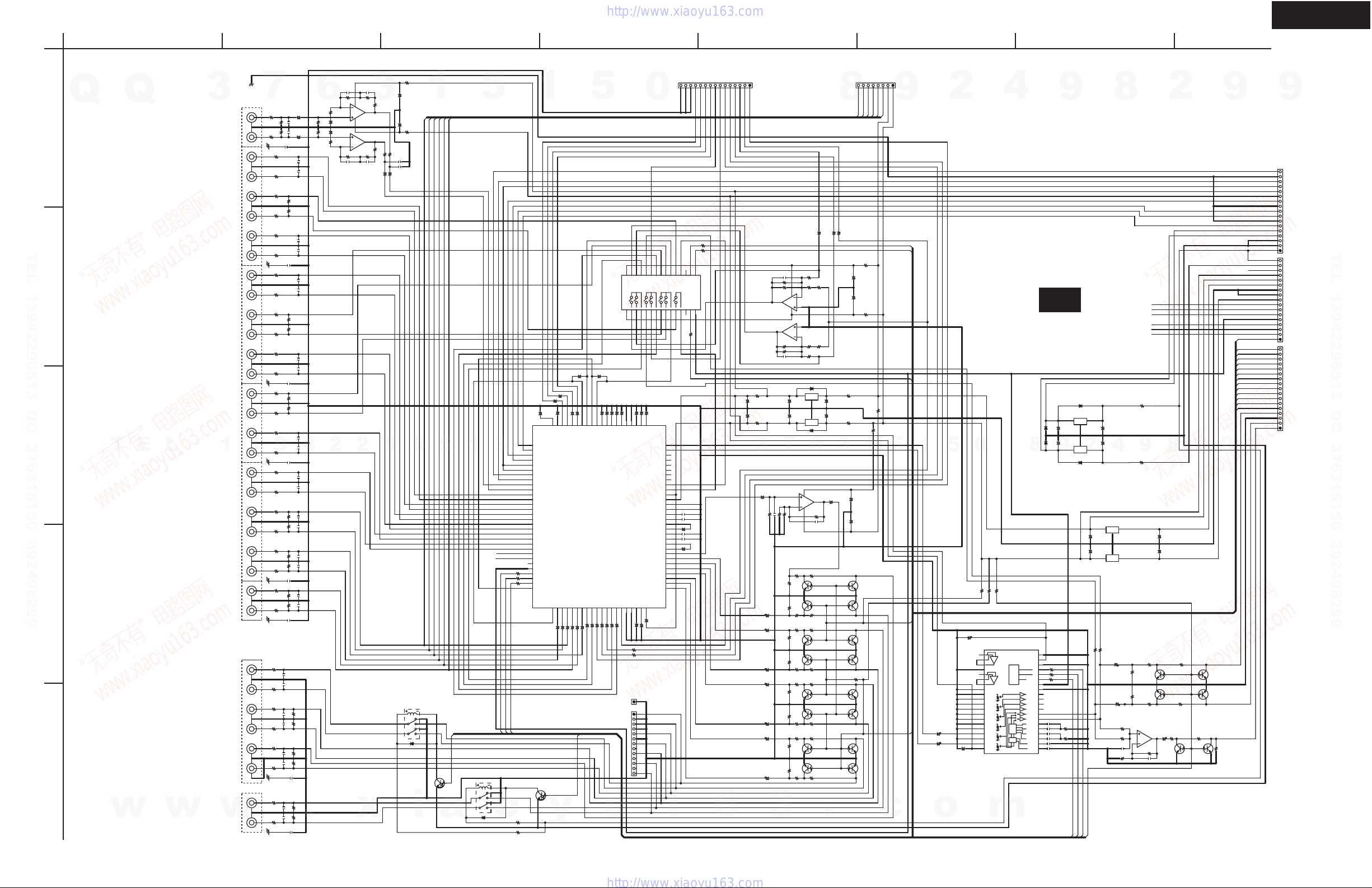
DTR-7.6
A
BCDEFGH
SCHEMATIC DIAGRAM 4
PREAMPLIFIER SECTION
Q
Q
1
TEL 13942296513 QQ 376315150 892498299
2
3
4
5
T
E
w
L
w
3
PHONO
CD
TAPE_OUT
TAPE
VIDEO3
VIDEO2_OUT
VIDEO2
VIDEO1_OUT
VIDEO1
DVD
SL/SR
C/SW
SBL/SBR
FL/FR
SL/SR
PREOUT
C/SW
SBL/SBR
1
w
1
P3001
P3002
P3003
P3004
3
P3005
1
P3006
P3008
1
P3009
P3010
7
3
2
9
7
8
6
4
5
3
1
2
9
7
8
6
4
5
3
1
2
6
4
5
3
1
2
9
7
8
6
4
5
3
1
R3041
2
3
2
9
100
7
8
100
6
100
4
5
100
3
1
2
11
3
100
2
100
R3124
330
R3126
56K
R3125
56K
R3123
C3051
102J
R3002
330
R3001
330
R3006
330
R3005
330
R3010
330
R3009
330
10
R3014
330
R3013
330
R3018
330
R3017
330
R3022
330
R3021
330
10
R3026
330
R3025
330
R3030
330
R3029
330
7
R3034
330
R3033
330
R3038
330
R3037
330
56K
R3042
330
330
10
R3046
330
R3045
330
4
R3054
R3053
R3058
R3057
102J
R3062
100
R3061
100
10
R3066
R3065
4
330
C3006
221J
9
C3054
221J
221J
R3040
R3039
R3043
R3048
C3029
C3031
C3057
C3034
C3033
102J
C3058
C3036
47/25
C3114
102J
C3113
102J
C3035
47/25
C3002
221K
221K
C3001
R3008
56K
56K
R3007
221J
C3052
221J
221J
R3020
56K
56K
R3019
C3012
C3053
R3028
56K
56K
R3027
C3016
C3018
C3017
56K
R3044
56K
R3047
C3028
C3027
C3030
102J
102J
C3032
102J
+
+
4
56K
56K
.
102J
6
R3070
R3069
C3005
221J
102J
C3008
C3007
221J
C3011
221J
102J
V1_RO
V1_LO
C3015
221J
102J
C3020
221J
C3019
221J
C3022
221J
C3021
C3055
56K
C3024
221J
C3023
C3111
102J
102J
102J
R3060
220K
R3059
R3063
102J
102J
220K
R3068
R3067
220K
R3074
270K
470K
R3072
470K
R3071
221J
221J
220K
R3064
C3042
123J
560
C3038
+
220/10
+
220/10
C3037
560
C3041
V2_RO
V2_LO
2
102J
220K
220K
2
3
5
6
R3073
270K
123J
C3044
392J
8
1
Q3001:A
4
NE5532
Q3001:B
NE5532
7
1.2K
R3075
22K
C3043
392J
2
x
R3076
3
22K
R3078
1.2K
R3077
R3079
+
10/50
C3045
9
100
R3080
+
C3046
R3081
+
47/25
C3047
47/25
C3048
+
R3082
10
100
101J
C3050
101J
10/50
RL3201
1
4
9
D3201
1SS352
Q3251
RN1402
C3049
6
i
10
1
MSR
MSL
12
3
5
10
8
MCT
MSW
MSBR
5
a
MSBL
SPRLF
D3202
1
RL3202
1SS352
5
PHONOL
R3087
220
1
4
9 8
MIC
PHONOR
VIDEO4L
VIDEO4R
3
TAPEL
TAPER
V1L
TUNERL
TUNERR
VLDATA
12
3
5
10
o
XML
XMR
TUPACKR
TUPACKL
CDL
CDR
V3L
V3R
V2L
V2R
V1R
DVDL
DVDR
R3086
220
R3088
220
C3132~C3137
C3071,C3072
C3079~C3083
10/50
VLSTB
VLCLK
R3251
(1/2W)
120
R3252
1
C3060
+
10/50
ADRT-
ADRT+
C3123
C3124
51
52
53
54
55
56
57
58
59
60
61
62
63
64
65
66
67
68
69
70
71
72
73
74
75
76
77
78
79
80
ADLT+
ADLT-
47/25
+
+
47/25
47/25
C3062
C3061
+
10/50
10/50
L1IN
R1IN
L2IN
R2IN
L3IN
R3IN
L4IN
R4IN
L5IN
R5IN
L6IN
R6IN
L7IN
R7IN
L8IN
R8IN
L9IN
R9IN
L10IN
R10IN
L11IN
R11IN
L12IN
R12IN
NC
DGND
DATA
CLOCK
LATCH
LAIN
Q3252
RN1402
120
C3121
C3122
+
+
+
47/25
46
47
49
50
48
43
44
45
FL-
FR-
FL+
FR+
VSS
VDD
DCR_IN
RAIN82CAIN83LSAIN84RSAIN85LBAIN86RBAIN87SWAIN88LBIN89RBIN90CBIN91LSBIN92RSBIN93LBBIN94RBBIN95SWBIN96GND97GND98VSS299VDD2
81
+
+
+
+
+
+
C3132
C3071
C3133
C3134
C3135
C3137
C3136
SPRLSB
y
(1/2W)
5
+
C3070
+
42
40
41
DCL_IN
DCL_OUT
DCR_OUT
DCCAP_SW
Q3003
NJW1157
+
+
+
+
C3072
C3080
C3079
Q3002
NJU7311AM
TAPE_LO
V1_LO
C3059
10/50
C3067
C3068
C3069
+
+
+
37
38
39
DCCAP_LB
DCCAP_RS
DCCAP_RB
30:REC_B2R
+
+
C3081
C3082+C3083
u
30
28
VDD
VSS
1
2345678
C3066+C3065
+
33
34
36
GND35GND
DCCAP_C
DCCAP_LS
+
C3085
10/50
R3129
R3130
P5003B
1
1
2
3
P5004B
4
5
6
7
8
9
10
11
12
13
0
DACSBR
27
25
S426S3
S229S1
COM1
DACSBL
C3063~C3070
47/25
C3064
C3063
+
+
31
32
DCCAP_L
DCCAP_R
REC_B2L
REC_B1R
REC_B1L
REC_A3R
REC_A3L
REC_A2R
REC_A2L
REC_A1R
REC_A1L
FIL_TR
FIL_BR
DC_R2
DC_R1
FIL_TL
FIL_BL
DC_L2
DC_L1
SWOUT
RBOUT
LBOUT
RSOUT
LSOUT
COUT
ROUT
LOUT
TCCAP
100
+
+
C3087
C3086
10/50
V1_RO
V2_RO
24
22
S623S5
COM2
9
30
29
Q
28
27
26
25
24
23
22
21
20
V-
19
V+
18
NC
17
NC
16
15
14
13
12
11
10
9
8
7
6
5
4
3
2
1
1/50
0
0
1
RECRRECL
TAPE_RO
21
20
COM3
101112
15
GNDA
19
S7
COM4
REC_R
REC_L
C3093
C3092
C3091
+
C3090
C3089
+
GNDA
GNDA
R3083
18
17
NC
NC14STB15GND
13
R3085
Z2R
Z2L
C3088
ADRT-
220
R3084
220
16
CLK
DATA
Q
1011121314
ADRT+
ADLT-
220
224J
472J
224J
P3101A
ADLT+
DACSBR
472J
4.7/50
4.7/50
6
DACSR
DACSBL
SROUT
SLOUT
DACR
DACSL
COUT
ROUT
LOUT
123456789
DACC
DACSW
DACL
Q3004:B
R3127
+
+
R3128
SBROUT
SBLOUT
C3103
R3097
10K
DMIXL
DMIXR
C3097
470/16
C3096
470/16
3
C3105
10/50
C3206
C3205
C3204
C3203
C3202
C3201
47/50
C3200
10K
Q3004:A
NE5532
10K
R3098
10K
10
10
+
47K
R3103
47/50
47/50
47/50
47/50
47/50
47/50
3
FSWDATA
FSWCLK
330J
R3099
8
7
4
NE5532
1
R3100
C3104 330J
1SS352
+
C3115
220/10
C3116
+
220/10
D3006
7
Q3007:A
221J
1.2K
C3106
R3104
R3105
R3227
220K
R3217
220K
R3216
R3226
R3225
220K
R3215
270
220K
R3214
R3224
R3223
270
220K
R3213
220K
R3212
R3222
R3221
270
220K
R3211
220K
270
R3210
R3220
R3095
6
5
3
2
D3005
3
2
15K
270
270
270
270
R3093
470
R3094
470
1
O
3
O2I
4
NE5532
R3106
8
10K
C3107
C3077
10K
R3092
G
2
1
G
1SS352
6
103K
R3237
Q3207
RN1443
RN1443
Q3206
100
R3236
R3235
100
Q3205
RN1443
RN1443
Q3204
R3234
100
R3233
100
Q3203
RN1443
Q3202
RN1443
R3232
R3231
100
Q3201
RN1443
RN1443
Q3200
R3230
100
+
10/50
R3091
1.2K
1.2K
R3096
3
I
1
100
100
C3078
10K
FSWSTB
Q3005
78L07
+
C3098
10/50
C3099
+
10/50
Q3006
79L07
C3108
10/50
RN1443
.
8
+
+
10/50
3
+
Q3217
Q3216
SBZ2MUT
RN1443
Q3215
Q3214
RN1443
Q3213
RN1443
Q3212
RN1443
Q3211
Q3210
RN1443
47/25
C3084
+
+
R3117
22
(1/2W)
R3118
22
(1/2W)
+
C3109
+
C3110
R3112
AMUT
RN1443
P3102A
8765432
MCT
MSL
MSW
MSBL
MSR
R3089
22
C3100
220/25
C3101
220/25
R3090
22
R3102
22
1
220/25
220/25
RN1443
0
c
+12V
MSBR
R3101
22
1
9
-12V
5
1
Z2R
Z2L
C3401
o
C3402
10/50
10/50
2
5
+
C3403
47/25
0
R3119
C3404
47/25
100K
1
2
4
5
6
7
8
9
10
11
12
13
14
15
16
17
18
19
20
3
AGND1
AGND2
INSW
AGND3
INSR
AGND4
INSL
AGND5
INC
AGND6
INFR
AGND7
INFL
VEE
4
NAAF-8678(1/2)
D3940
1SS352
D3941
1SS352
8
100K
R3121
R3120
100K
Q3009
BD3814
AGND10
-
+
VCC
LOGIC
AGND9
CL
-
DA
+
MUTE
DGND
AGND8
OUTSW
OUTSR
OUTSL
OUTC
OUTFR
OUTFL
BNF2L
BNF1L
BASS
BNF2R
BNF1R
TNFL
TREBLE
TNFR
m
U06
40
39
R3401
38
37
36
R3402
35
34
R3403
33
32
31
30
C3405~
29
C3408
28
104J
27
26
C3405
25
C3406
24
C3407
23
C3408
22
21
C3409
C3410
472J
9
D3938
1SS352
Q3505
LM2940CT-5.0
+
C3945
100/10
C3946
+
10/50
9
Q3506
NJM7905FA
D3939
+12V
-12V
100
100
100
R3404
4.7K
R3405
4.7K
472J
3
O
G
2
C3944
C3943
1
3
G
O2I
1SS352
C3942
10/50
Z2VMUT
Z2VCLK
Z2VDATA
1
I
10/50
10/50
2
Z2MUT
+
+
Q3507
NJM7812FA
3
+
C3941
10/50
+
3
NJM7912FA
0
R3113
C3411
22/50
22/50
C3412
R3418
C3415
8
4
O
2
1
O I
Q3508
0
R3114
R3417
4.7K
103K
103K
R3419
2
To schematic 5
R3509
0.22
(1/2W)
8
9
R3510
0.22
(1/2W)
1
I
G
G
R3407
R3408
47K
22K
22K
5
6
R3409
470
R3410
470
Q3007:B
NE5532
R3420
C3416
103K
7
C3939
+
10/50
+
C3940
10/50
C3417
4.7/50
4.7K
R3411
220
Q3401
RN1443
Q3402
RN1443
R3412
220
R3421
270
Q3405
RN1443
2
Q3403
RN1443
Q3404
RN1443
R3422
100
Q3406
RN1443
9
9
22K
R3423
VIDEO4L
GNDV4
VIDEO4R
MIC
+7V
-7V
TUPACKL
GNDTU
TUPACKR
XML
XMAGND
XMR
+5VVIDEO
-5VVIDEO
GNDV
GNDV
+9V
+9V
-9V
VPOWER
-12V
+12VTRG
+22V
GNDRL
GNDRL
-22V
SEC1H
VOLH
PROTECT
GNDDG
HPL
HPE
HPR
SPRLF
AMUT
Z2MUT
SBZ2MUT
SPRLSB
FSWDATA
FSWCLK
FSWSTB
VLSTB
VLDATA
VLCLK
Z2VCLK
Z2VDATA
Z2VMUT
Z2POL
Z2GND
Z2POR
Z2SWPO
9
9
17
16
15
14
13
12
11
10
9
8
7
6
5
4
3
2
1
17
16
15
14
13
12
11
10
9
8
7
6
5
4
3
2
1
17
16
15
14
13
12
11
10
9
8
7
6
5
4
3
2
1
P3103A
P3104A
P3105A
TEL 13942296513 QQ 376315150 892498299
Page 14
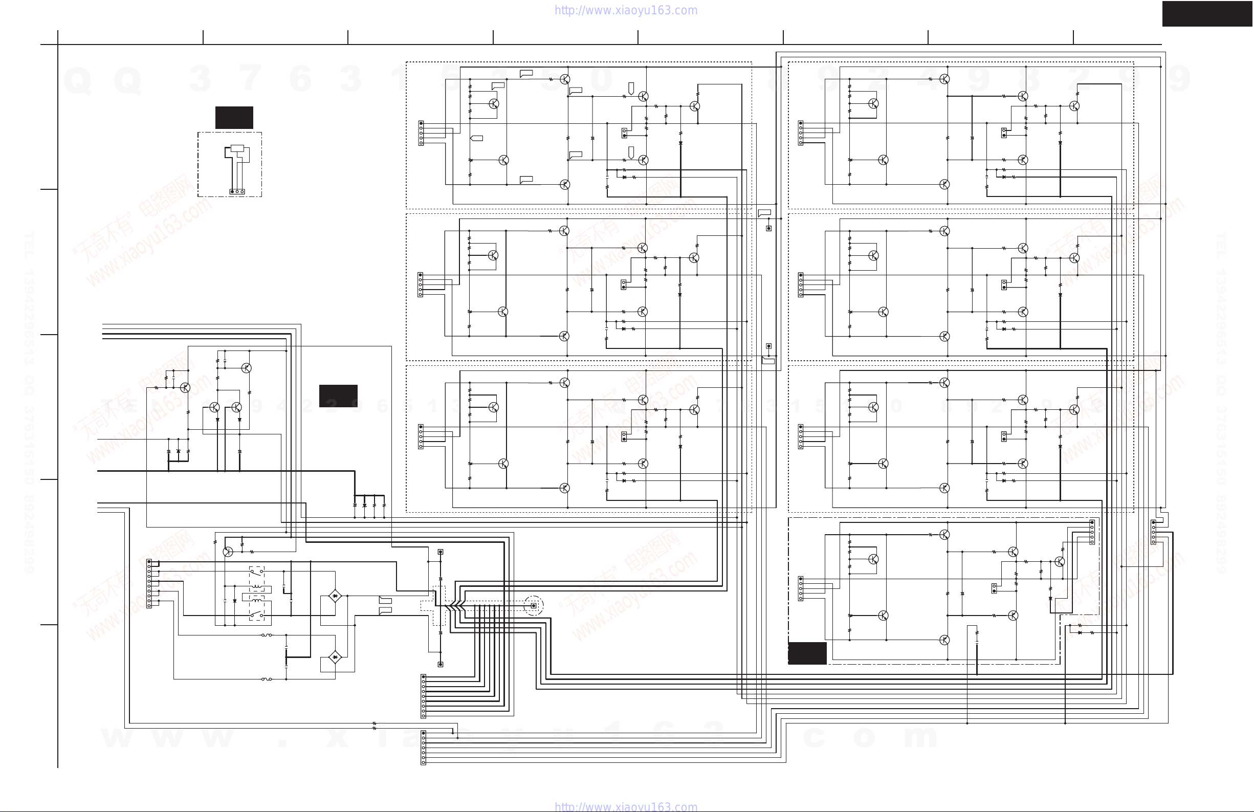
DTR-7.6
A
BCDEFGH
SCHEMATIC DIAGRAM 5
POWER AMPLIFIER SECTION
U062
1
10K
R6707
R6708
3
D6702
(1/2W)
RL6901
102J
C6911
7
3
G
V
O
2
+5VDIS
GNDDG2
123
THERMAL
C6705
223Z
2SA1162-GR
33K
2SC2712-GR
9
D6701
1SS133
+
220/16
C6701
R6903
47K
R6902
2SC2712-GR
Q6707
4
3 2
3
D6902
1SS352
4 1
RL6902
12A-TUL-250V
12A-TUL-250V
Q6704
R6705
Q6701
1K
F6901
F6902
18K
1
2
6
4
C6912
334J/100V
C6915
C6916
.
U06
2
2
NAAF-8678
4
C6913
334J/100V
D6901
D10XB60H
334J
4
334J
D10XB60H
x
3
2
D6903
3
10/50
C6706
1
2
1
3
9
+
Q
Q
3
1
NAETC-8680
Q6380
LM61CIZ
JL703A
TEL 13942296513 QQ 376315150 892498299
2
VOLH
SEC1H
GNDRL
+22V
223Z
C6703
10K
R6702
R6701
22K
3
T
PROTECT
GNDDG
HPE
HPR
HPL
4
E
2SA1163-BL
L
C6704
1
2
3
P6952A
4
5
6
7
8
9
10
5
w
w
Q6703
1/50
GND
S1H+
S1HS1L+
S1L-
UDZS5.1B
+
D6703
2SC2712
-GR
Q6702
47K
R6704
R6706
1
1SS133
220K
0.22
R6197
w
6
5.6K
UDZS5.1B
R6709
D6704
57.2
-57.2
R6180
390
(1/2W)
R6181
390
i
(1/2W)
1
18K
R6710
5
-B
a
L
P6000A
NFL
1
-BSL
2
+BSL
3
L+
4
L-
5
R
P6001A
NFR
1
-BSL
2
+BSL
3
R+
4
R-
5
c
1
P6002A
NFC
1
-BSL
2
+BSL
3
C+
4
C-
5
+B
1
2
3
4
5
JL6603A
6
7
8
9
1
2
3
4
5
6
JL6600A
7
5
P6901A
1
+
+
C6902
1
P6902A
SPLSPRSPCSPSLSPSRSPSBLSPSBRGNDRL
+22V
SPL+
SPR+
SPC+
SPSL+
SPSR+
SPSBL+
SPSBR+
R6010
R6020
R6011
R6021
R6012
3
R6022
15000/71
C6901
15000/71
o
R6030
5.6K
3.9K
-0.5
R6040
2K(B)
R6050
R6031
5.6K
3.9K
R6041
2K(B)
R6051
R6032
5.6K
3.9K
R6042
2K(B)
R6052
1
470
3.3K
470
3.3K
470
3.3K
P6911A
1.1
Q6000
2SC1740S_S
2SC1740S_S
Q6001
2SC1740S_S
Q6011
2SC1740S_S
Q6002
2SC1740S_S
Q6012
2SC1740S_S
y
1.1
Q6010
-1.0
R6120
2.2
5
(1/4W)
R6070
Q6040
2SA1930
R6121
2.2
(1/4W)
R6071
Q6041
2SA1930
R6122
2.2
(1/4W)
R6072
Q6042
2SA1930
u
82
82
82
2SC5171
(1/4W)
2SC5171
(1/4W)
2SC5171
(1/4W)
Q6030
0.6
-0.6
Q6031
Q6032
0
+
47/50
C6020
473J
C6030
8.2
R6130
+
47/50
C6021
473J
100V
C6031
8.2
(1W)
R6131
+
47/50
C6022
473J
100V
C6032
8.2
R6132
1
R6080
0.22
(1/4W)
P6080
ID+
ID-
R6090
(1/4W)
100V
(1W)
P6081
ID+
ID-
1SS133
Q
P6082
ID+
ID-
(1W)
0.22
R6190
D6000
1SS133
R6081
0.22
(1/4W)
R6091
0.22
(1/4W)
R6191
D6001
R6082
0.22
(1/4W)
R6092
0.22
(1/4W)
R6192
D6002
1SS133
0.6-0.6
2
1
R6210
2
1
R6211
Q
2
1
R6212
Q6050
MN150S
R6140
22K
R6100
0.22*2
(5W)
Q6060
MP150S
47K
47K
Q6051
MN150S
R6141
22K
R6101
0.22*2
(5W)
Q6061
MP150S
47K
47K
Q6052
MN150S
R6142
22K
R6102
0.22*2
(5W)
Q6062
MP150S
47K
47K
6
12K
R6150
1SS133
12K
R6151
D6011
1SS133
12K
R6152
1SS133
D6010
D6012
R6160
33K
2SC2229-Y
R6240
220K
Q6071
2SC2229-Y
R6161
33K
Q6071
R6241
220K
Q6072
2SC2229-Y
R6162
33K
Q6072
3
R6242
220K
3
Q6070
7
6
.
8
57.2
1
1
-57.2
3
P6901B
P6902B
SL
P6003A
NFSL
1
-BSL
2
+BSL
3
SL+
4
SL-
5
SR
P6004A
NFSR
1
-BSL
2
+BSL
3
SR+
4
SR-
5
SBL
5
1
P6005A
NFSBL
1
-BSL
2
+BSL
3
SBL+
4
SBL-
5
JL6006B
1
NFSBR
-BSBR
2
+BSBR
3
SBR+
4
SBR-
5
U064
c
9
R6013
R6023
R6014
R6024
R6015
1
R6025
R6016
R6026
R6033
2
470
5.6K
3.9K
R6053
5.6K
3.9K
R6054
5.6K
3.9K
R6055
R6036
470
5.6K
3.9K
R6046
R6056
R6043
R6034
R6044
R6035
R6045
1K(B)
2K(B)
3.3K
470
2K(B)
3.3K
470
2K(B)
3.3K
2SC1740S_S
3.3K
5
Q6006
Q6003
2SC1740S_S
2SC1740S_S
2SC1740S_S
2SC1740S_S
Q6005
0
2SC1740S_S
2SC1740S_S
Q6016
2SC1740S_S
NAAF-8682
o
Q6013
Q6004
Q6014
Q6015
(1/4W)
m
R6123
4
(1/4W)
Q6043
2SA1930
R6124
(1/4W)
Q6044
2SA1930
R6125
(1/4W)
Q6045
2SA1930
R6126
2.2
Q6046
2SA1930
2.2
R6073
2.2
R6074
2.2
R6075
150
(1/4W)
150
(1/4W)
8
220
(1/4W)
220
R6076
Q6033
2SC5171
Q6034
2SC5171
Q6035
2SC5171
Q6036
2SC5171
(1/4W)
9
+
C6023
473J
C6033
8.2
R6133
+
C6024
473J
C6034
8.2
R6134
9
+
C6025
473J
C6035
8.2
R6135
2SC5359_O
+
47/50
C6026
P6083
47/50
100V
(1W)
P6084
47/50
100V
(1W)
47/50
100V
(1W)
R6086
0.22
(1/4W)
P6086
ID+
ID-
R6096
0.22
(1/4W)
R6136
8.2
C6036
473J
100V
R6083
0.22
(1/4W)
ID+
ID-
R6093
(1/4W)
D6003
1SS133
R6084
0.22
(1/4W)
ID+
ID-
R6094
(1/4W)
D6004
1SS133
R6085
0.22
(1/4W)
2
P6085
ID+
ID-
R6095
(1/4W)
D6005
1SS133
Q6056
2
1
(1W)
2
1
0.22
R6193
R6213
2
1
0.22
R6194
R6214
2
1
0.22
R6195
R6215
Q6053
MN150S
8
R6143
22K
R6103
0.22*2
(5W)
Q6063
MP150S
47K
47K
Q6054
MN150S
R6144
22K
R6104
0.22*2
(5W)
Q6064
MP150S
47K
47K
Q6055
MN150S
R6145
22K
4
R6105
0.22*2
(5W)
Q6065
MP150S
47K
47K
Q6076
2SC2631R
R6146
22K
R6156
12K
R6106
0.22*2
R6246
(5W)
D6016
1SS133
Q6066
2SA1987_O
9
R6153
R6154
R6155
R6166
33K
220K
2
12K
R6243
220K
D6013
1SS133
12K
R6244
220K
D6014
1SS133
Q6075
2SC2229-Y
8
12K
R6245
220K
D6015
1SS133
R6196
47K
R6163
33K
Q6073
2SC2229-Y
R6164
33K
Q6074
2SC2229-Y
R6165
33K
2
Q6075
1
2
3
4
5
R6216
47K
D6006
1SS133
JL6200B
9
9
9
9
1
2
3
4
5
JL6200A
TEL 13942296513 QQ 376315150 892498299
Page 15
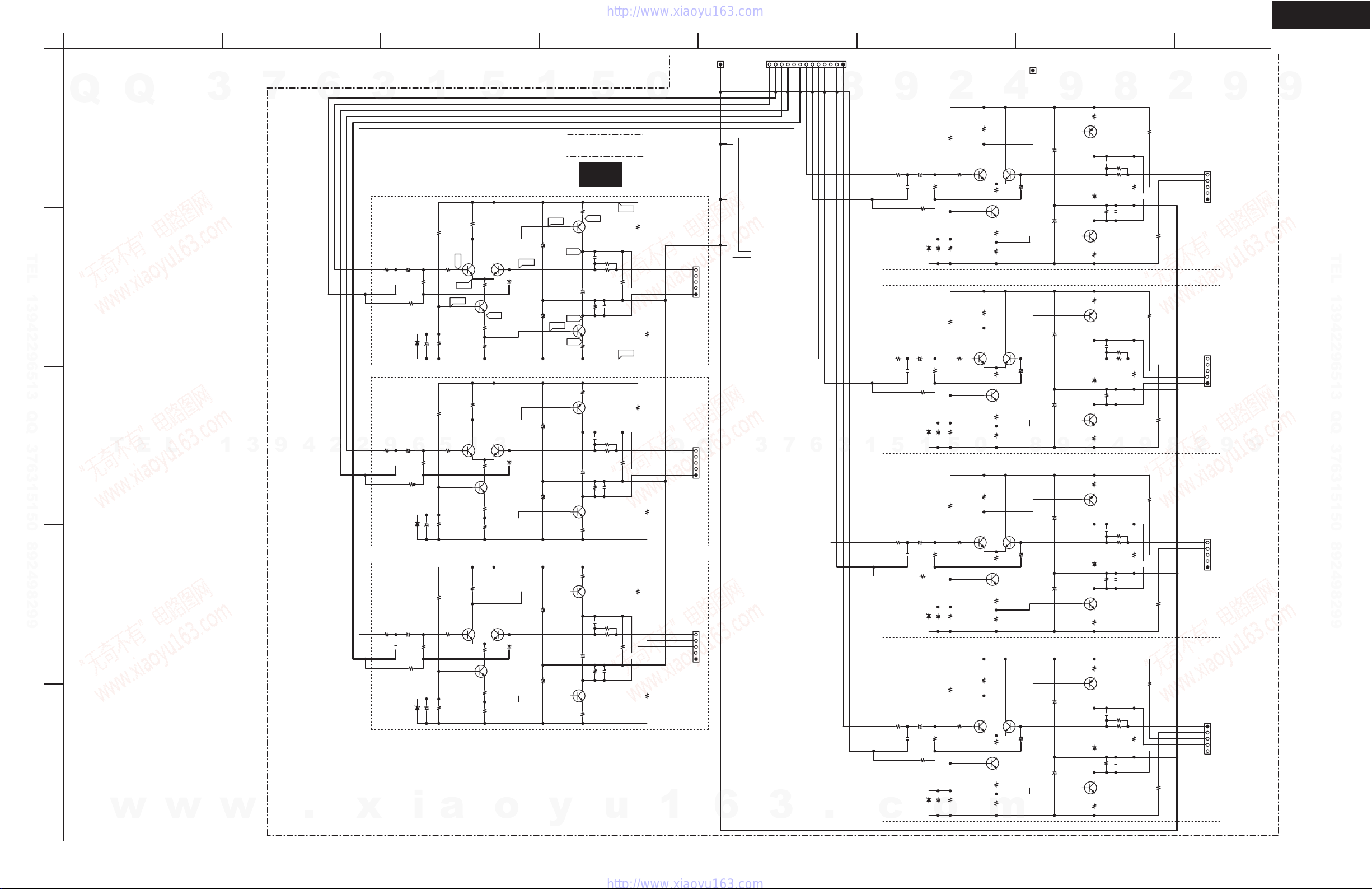
DTR-7.6
A
BCDEFGH
SCHEMATIC DIAGRAM 6
DRIVER SECTION
3
7
9
4
.
6
2
3
2
x
R5000
R
R5001
1K
9
R5002
1K
1K
C5000
C5001
C5002
Q
Q
3
1
TEL 13942296513 QQ 376315150 892498299
2
3
4
5
T
E
w
L
w
1
w
L
C5010
47/50
+
221K
R5040
2.2K
D5000
MTZJ5.6B
C5011
47/50
+
6
221K
R5041
2.2K
D5001
MTZJ5.6B
C
C5012
47/50
+
221K
R5042
2.2K
MTZJ5.6B
i
R5010
C5020
R5011
10/50
D5002
1
R5090
100K
2SC1845-E
R5020
330
56K
10/50
+
R5100
R5091
2SC1845-E
5
R5021
330
56K
+
C5021
100K
R5092
2SC1845-E
R5022
56K
R5012
10/50
+
C5022
a
Q
5000
-51.2
100K
100K
Q5001
R5101
100K
Q5002
330
R5102
0
-0.6
R5051
R5052
100K
R5110
R5080
R5111
1
4.7K
R5061
R5081
R5112
4.7K
5
1K
R5060
470
1K
1.2K
470
1K
470
R5082
Q5010
2SC1845-E
+
4.7K
R5050
Q5050
2SC1845-E
-51.8
1.2K
Q5011
2SC1845-E
3
+
Q5051
2SC1845-E
Q5012
2SC1845-E
+
Q5052
2SC1845-E
1.2K
R5062
o
0
C5040
220/25
C5041
220/25
C5042
220/25
1
+
+
C5110
10/100
+
+
C5111
+
+
55.3
10/100
C5100
R5130
-55.5
R5170
(1/4W)
C5101
10/100
R5131
10/100
C5102
10/100
R5132
C5112
10/100
y
22K
-55.9
100
22K
22K
1.1
-1.0
5
NAAF-8668
U045
R5160
C5080
040C
+
C5050
Q5040
2SC2229-Y
R5161
2SA949Y
C5081
040C
+
C5051
Q5041
R5171
R5162
(1/4W)
Q5032
2SA949Y
C5082
040C
+
C5052
2SC2229-Y
100
(1/4W)
55.8
Q5030
2SA949Y
R5030
120K
R5230
120K
47/50
C5090
101K
100
(1/4W)
Q5031
R5031
120K
R5231
120K
47/50
R5201
C5091
101K
2SC2229-Y
100
(1/4W)
100
R5032
120K
R5232
120K
47/50
C5092
101K
Q5042
100
R5172
(1/4W)
56.5
R5200
-56.5
22K
R5182
R5202
u
22K
10
(1/4W)
22K
0
10
R5180
R5190
R5181
R5191
(1/4W)
10
10
(1/4W)
(1/4W)
10
(1/4W)
10
(1/4W)
R5192
1
NFL
-B1L
+B1L
B+L
B-L
NFR
Q
-B1R
+B1R
B+R
B-R
NFC
-B1C
+B1C
B+C
B-C
5
4
3
2
1
5
4
3
2
1
5
4
3
2
1
Q
P5503A
1
AGND
P6000A
P6001A
P6002A
6
SCREW
TERMINAL
4
Q5013
2SC1845-E
+
Q5053
2SC1845-E
1.2KK
Q5014
2SC1845-E
+
Q5054
2SC1845-E
1.2K
Q5015
2SC1845-E
+
Q5055
2SC1845-E
1.2K
P5019
220/25
C5043
C5044
220/25
8
C5045
220/25
9
+
+
+
+
C5114
9
+
C5105
+
C5103
10/100
C5113
10/100
C5104
10/100
10/100
10/100
C5085
C5115
10/100
R5163
C5053
R5133
22K
R5134
22K
2
040C
R5135
22K
C5083
+
47/50
2SC2229-Y
R5173
R5164
Q5034
2SA949Y
C5084
+
C5054
Q5044
2SC2229-Y
R5174
R5165
2SA949Y
+
C5055
Q5045
2SC2229-Y
R5175
8
120
(1/4W)
Q5033
2SA949Y
R5033
120K
040C
R5233
120K
C5093
101K
Q5043
120
(1/4W)
120
(1/4W)
R5034
120K
040C
R5234
120K
47/50
C5094
101K
120
(1/4W)
4
120
(1/4W)
Q5035
R5035
120K
R5235
120K
47/50
C5095
101K
120
(1/4W)
R5203
R5204
9
R5205
R5183
22K
R5184
22K
R5185
22K
10
R5193
10
R5194
10
R5195
2
(1/4W)
10
(1/4W)
(1/4W)
10
(1/4W)
8
(1/4W)
10
(1/4W)
NFSL
-B1SL
+B1SL
B+SL
B-SL
NFSR
-B1SR
+B1SR
B+SR
B-SR
NFSBL
-B1SBL
+B1SBL
B+SBL
B-SBL
2
9
5
4
3
2
1
P6003A
9
TEL 13942296513 QQ 376315150 892498299
5
4
3
2
1
P6004A
9
9
5
4
3
2
1
P6005A
P5004A
SR
AGND
6
SBL
AGND
123456789
8
SBR
AGND
3
1
9
R5003
1K
R5004
1K
R5044
5
R5005
1K
SL
C5003
R5043
2.2K
SR
C5014
2.2K
D5004
SBL
C5015
47/50
C5005
221K
R5045
2.2K
C5013
47/50
+
221K
D5003
MTZJ5.6B
47/50
+
C5004
221K
MTZJ5.6B
1
+
D5005
MTZJ5.6B
+
R5094
+
C5024
R5095
R5015
10/50
+
C5025
2
R5093
2SC1845-E
R5023
56K
R5013
10/50
C5023
100K
2SC1845-E
R5024
56K
R5014
10/50
R5104
5
100K
Q5005
2SC1845-E
R5025
330
56K
R5105
100K
Q5003
330
100K
R5103
Q5004
330
100K
100K
R5113
R5053
4.7K
R5114
R5054
4.7K
0
R5115
R5055
4.7K
R5085
1K
R5063
470
R5083
1K
R5064
470
R5084
1K
R5065
470
101112
13
R
L
AGND
C
SL
AGND
1
BUS
P6011B
Val
2
3
7
3
SBR
120
R5166
R5136
22K
(1/4W)
Q5036
2SA949Y
040C
C5086
R5236
120K
+
47/50
C5056
Q5046
2SC2229-Y
120
R5176
R5036
120K
C5096
101K
(1/4W)
22K
R5206
R5186
10
(1/4W)
10
R5196
NFSBR
-B1SBR
+B1SBR
B+SBR
B-SBR
(1/4W)
1
2
3
4
5
JL6006A
3
.
R5006
1K
c
C5016
47/50
C5006
R5046
2.2K
D5006
+
221K
MTZJ5.6B
R5096
56K
R5016
10/50
+
C5026
o
100K
Q5006
2SC1845-E
R5026
330
100K
R5106
R5116
R5056
4.7K
R5086
m
1K
Q5056
2SC1845-E
1.2K
R5066
470
Q5016
2SC1845-E
+
C5046
220/25
+
C5106
+
C5116
10/100
10/100
Page 16
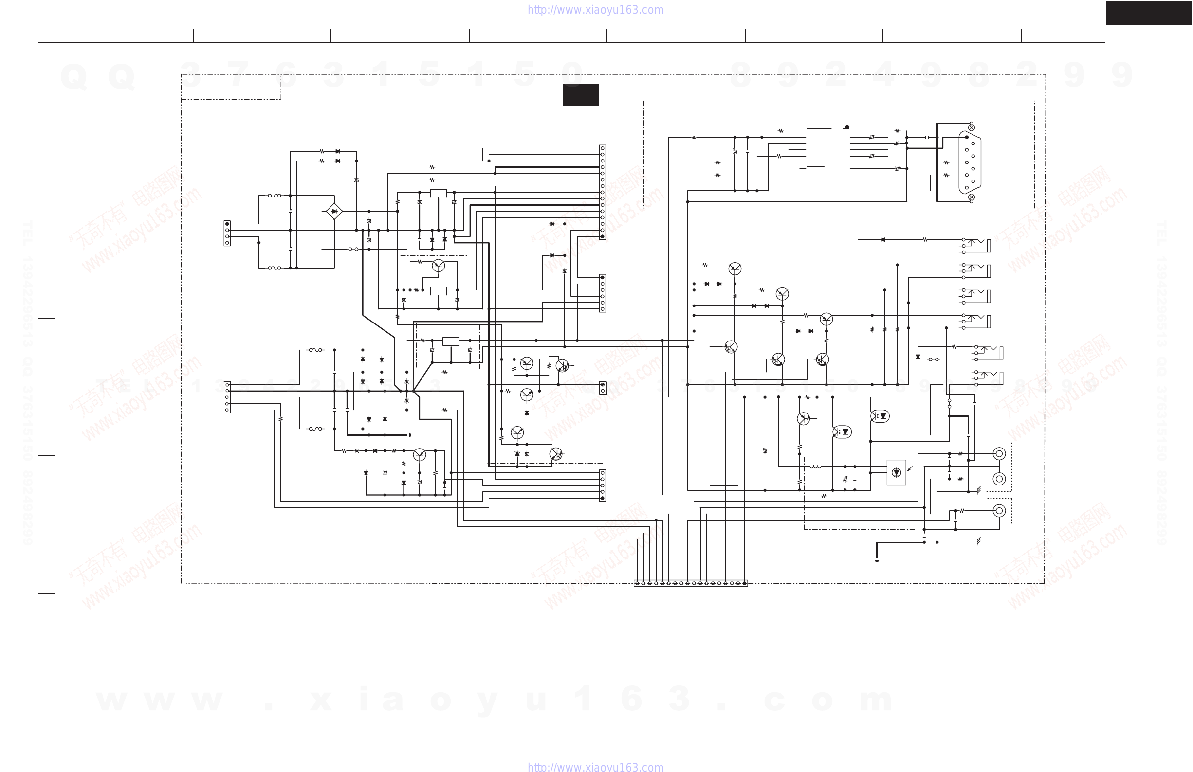
DTR-7.6
A
BCDEFGH
SCHEMATIC DIAGRAM 8
POWER SUPPLY SECTION
3
7
BROWN
1
2
P951
3
4
BROWN
1
2
3
P952
4
5
S2-
S3+
9
S3FLAC1A
FLAC2A
6
F951
6.3A-SE-EAK
BLACK
F952
6.3A-SE-EAK
GRAY
WHITE
4
GRAY
BLUE
BLUE
C951
C952
2
334J
334J
R961
R951
2.2
(1/2W)
R952
2.2
(1/2W)
D953
D10XB60H
F931
1.6A-SE-EAK
2
4.7 (1/2W)
F932
1.6A-SE-EAK
3
D951
1SS133
D952
1SS133
2
4
3
334J
C962
9
334J
C963
R962
2.2
(1/2W)
1
C964
220/50
Q
Q
3
NAPS-8665
1
TEL 13942296513 QQ 376315150 892498299
2
3
4
T
E
L
1
+
3.3/50
C953
10000/16
C954
J952
D963
RN1N4003
D965
6
102J
GNDS
D957
RN1N4003
+
C967
D956
RN1N4003
1
+9V
+
+
-9VVD
C955
3300/16
R955
RN1N4003
RN1N4003
5
-22V
D968
1SS355
R963
+
C968
220/63
0.22
(1W)
R967
+
C958
10/50
(1/4W)
2.2
(1/2W)
+22V
D964
RN1N4003
3300/35
+
D966
C965
1
D969
1SS355
22
(1/2W)
15K
D958
MTZJ33D
5
R953
R954
Q951
+
C929
R966
0.22
(1/2W)
R956
33
R969
0.22
(1/2W)
+
C966
1000/35
E5502
2SA965-Y
R964
+
0.22
2.2
LM2940CP-5.0
1
I
O
G
2
C956
10/50
1SS355
1SS355
102J
D970
2SA1930
D model
Q952
2
I
O
G
1
S812C53
12V POWER
TA7812S
1
I
+
10/50
C960
Q953
GNDA
3
R971
(1/2W)
Q954
-VP
33K
R965
C969
47/50
C970
(1W)
(1/2W)
3
100/16
D971
Q959
3
G
2
R970
2.2
(1W)
2.2
223Z
+
+
C959
3
O
1
C957
100/16
C961
+
XM POWER
10/50
R959
MTZJ-
8.2C
5
RN1N4003
D962
RN1N4003
GNDD
GND12
R957
2SA1015
2.2K
R946
10
(1/2W)
2.2K
D954
D961
Q957
FAN POWER
Q960
2SC1740S
+
GNDRL
R958
Q955
2SD1858
D967
1SS133
C974
10/50
GNDFL
+5VDSP
FLAC2
FLAC1
0
C973
470/16
1K
FANDC
-VP
U042
POFF2
+9VVD
+9VVD
GNDV
GNDV
-9V_VD
+5VDSP
+5VDSP
GNDD
GNDD
+5.3VXM
GNDD
+VMPU
POFF
APOWER
+
APOWER
+12V
10S
POFF
Q958
KRC102M
GNDD
Q
Q956
KRC102M
15
14
13
12
11
10
9
8
7
6
5
4
3
2
1
1
2
3
4
5
6
1
2
5
4
3
2
1
TO_MOTHER
P954B
JL911B
TO_PS1
Q
P955
JL957B
RS-232C
FANL
FANH
18
3
-22VA
GNDA
GNDA
L5501
022M
232TXD
232RXD
+12VTRG
7
GNDD
Z2L
Z2SW
+22VA
232RXD
232TXD
12
1314151617
TO_MOTHER
R5511
3.9
D5501
1SS355
DTC114ES
6
Z2R
AGND
P959B
R5503
330
R5502
330
D5502
1SS355
R5514
1K
Q5505
IRIN
12VTRG
8
C5501
Q5502
2SB1240
D5503
1SS355
3
12VTRGC
+56S
12VTRGA
12VTRGB
1234567891011
223Z
100/16
C5502
R5512
3.9
D5504
1SS355
R5515
Q5506
DTC114ES
1
C5511
9
R5505
10k
R5504
10k
Q5503
2SB1240
1K
5
100/16
GNDD
D5505
1SS355
DTA114ES
100
R5521
10K
R5522
ICL3221ECVZ
16
FORCEOFF
15
VCC
14
GND
13
T1OUT
12
FORCEON
11
T1IN
10
INVALID
9
R1OUT
R5513
3.9
D5506
1SS355
1
R5520
100K
Q5508
022M
L5502
IRRV
2
Q5501
Q5504
2SB1240
DTC114ES
5
Q5509
PC817X
R5524
1K
EN
C1+
C1-
C2+
C2-
R1IN
R5516
Q5507
4
100/16
V+
V-
1K
0
1
C5512
P5501
RS-232C
2
9
9
4
R5506
C5503
1
1/50
2
3
4
5
6
7
8
C5504
1/50
C5505
C5506
1/50
1/50
10k
9
223Z
C5507
R5507
GNDS
330
R5508
330
8
10
1
6
2
7
3
8
4
9
5
11
TEL 13942296513 QQ 376315150 892498299
223Z
C5513
D5507
IRLED
R5517
4
E5501
R5518
220K
2
3
1
GNDS
1
P5505
R5519
220K
8
Q5510
U5501
220K
D5508
PC817X
C5514
R5509
100
IRLED
9
102K
J5502
C5508
102J
C5509
102J
2
22
24
21
10
22
24
21
10
R5510
100
J5508
J5506
R5525
100
R5526
100
R5527
C5510
2
1
2
1
100
P5506
P5507
22
24
21
2
10
1
4
C5516
103Z
C5515
4
102J
3
P5505
9
103Z
3
2
2
IRIN A
12VTRGC
/Z2
12VTRGA
12VTRGB
IRIN B
IROUT
8
1
P5503
1
P5502
2
9
9
5
w
w
w
.
x
i
a
o
y
u
1
6
3
.
c
o
m
Page 17
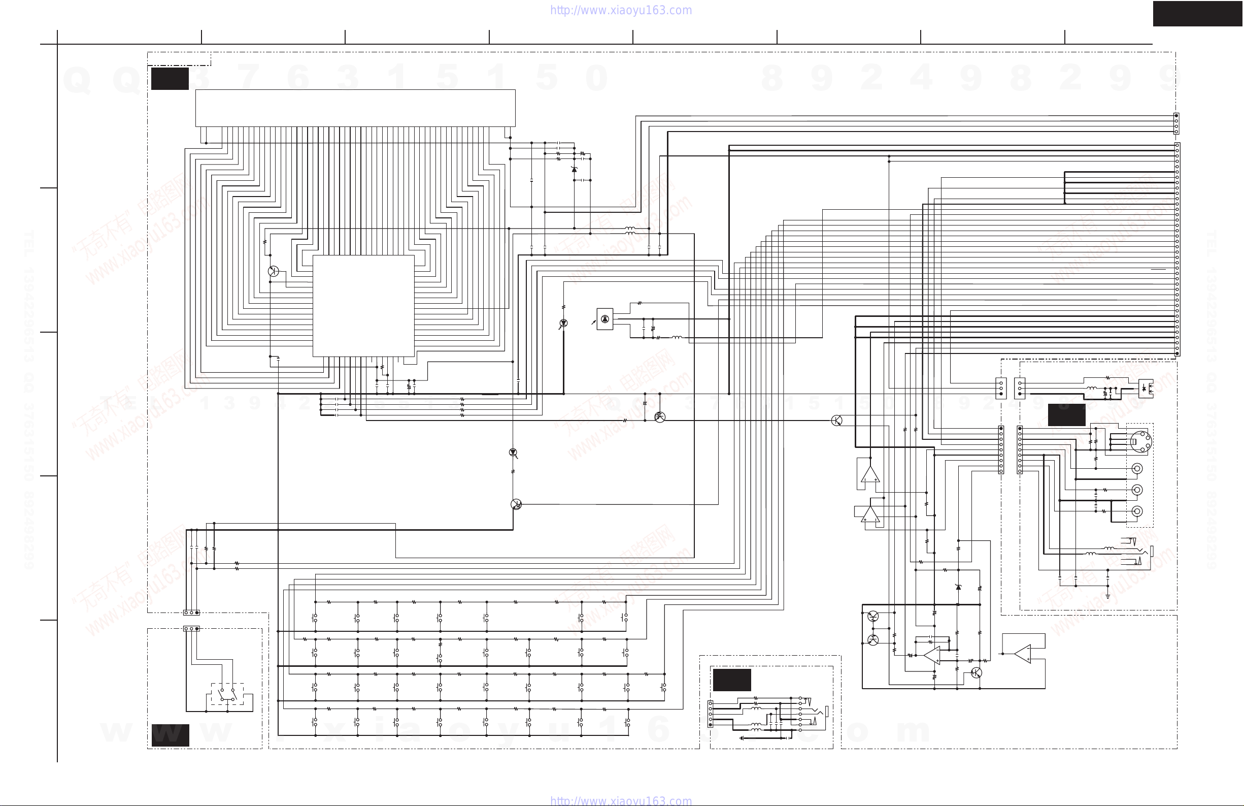
DTR-7.6
A
SCHEMATIC
NADIS-8683
BCDEFGH
DIAGRAM 9
DISPLAY
Q
Q
U07
3
SECTION
1
F1258F11
59
TEL 13942296513 QQ 376315150 892498299
2
3
4
5
T
E
w
L
U075
w
1
104Z
1K
C7591 104Z
C7592
R7545
123
JL7503A
1
2
3
JL7503B
VBJ#
VAJ#
DISGND#
S7591
4
w
NAETC-8687
7
1G542G533G524G515G506G497G488G479G4610G4511G4412G4313G4214G4115G4016G39P138P237P336P435P534P633P732P831P930P1029P1128P1227P1326P1425P1524P1623P1722P1821P1920P2019P2118P2217P2316P2415P2514P2613P2712P2811P2910P309P318P327P336P345P352F221F21
55
3
9
1K
10K
R7592
R7546
10K
R7591
3
1
5
2
100K
R7501
4
.
6
Q7503
2SC2712
C7514
C7515
C7516
C7517
C7518
104Z
2
VAJ
VBJ
STANDBY
R7581
TUN
MODE
49
50
51
52
53
54
55
56
57
58
59
60
61
62
63
64
101J
101J
101J
101J
S7501S7508
0
CD
SETUP
Q7501
SEG0
VCC2
DIG15/SEG39
DIG14/SEG38
DIG13/SEG37
DIG12/SEG36
DIG11
DIG10
DIG9
DIG8
DIG7
DIG6
DIG5
S7515
S7521
48
SEG3
DIG02
DIG03
1
2
R7551
330
x
3
HNA-16SM10T
42
SEG943SEG844SEG745SEG646SEG547SEG4
49:SEG2
50:SEG1
Q7502
M66005
64:DIG4
DIG005_RESET6_CS7SCK8SDATA9P110P011VCC112XOUT
DIG01
2
3
4
9
R7552
ZONE2
S7502
R7557
330
S7509
TUNER
R7563
330
S7516
MEMORY
R7568
330
S7522
RETURN
470
32:SEG19
31:SEG20
17:SEG33
104Z
C7519
6
R7564
R7569
i
1
VSS
XIN
131415
20
C75
101J
ZONE2
OFF
470
S7510
TAPE
470
S7517
DIMMER
470
PRESET
FR
SEG21
SEG22
SEG23
SEG24
SEG25
SEG26
SEG27
SEG28
SEG29
SEG30
SEG31
SEG32
SEG35
R7519
27K
C7521
100/6.3
5
S7503
S7523
a
33
SEG1834SEG1735SEG1636SEG1537SEG1438SEG1339SEG1240SEG1141SEG10
VP
SEG34
16
R7553
560
32
31
30
29
28
27
26
25
24
23
22
21
20
19
18
17
C7522
474J
ZONE
R7559R7558
PHONO
S7511
R7565
560
LIS
R7570
560
1
2V -
S7504
S7518
MODE>
DOWN
PRESET
5
R7520
R7521
R7522
3
R7523
R7554
820
0
R7582
R7571
820
S7524
o
3.3K
3.3K
220
220
ZONE
R7560
820
VIDEO4
S7512
R7566
820
LIS
PRESET
1
FLDRST
FLDCS
FLDCLK
FLDSDO
MICMUT
D7503
2V+
S7505
S7519
MODE<
S7525
UP
C7523
180
R7542
R7561
1.2K
VIDEO3
S7513
R7567
1.2K
R7572
1.2K
y
104Z
R7555
1.2K
STEREO
PRESET
FF
5
223Z
C7508
C7509
ZONE2
Q7506
RN1402
R7562
R7576
S7520
R7573
S7526
C7506
C7507 104Z
R7517
R7518
UDZS8.2B
104Z
R7556
2.2K
2.2K
2.2K
u
104Z
220
220
D7501
104Z
C7510
LEDZONE2
2.2K
VIDEO2
TONE+
C7511
33/50
C7513
473Z
LEDSBY
R7530
2.2K
D7502
STBY
S7507
MULTI
S7514
S7530
S7527
ENTER
0
C7512
473Z
U7501
R7580
3.9K
R7579
3.9K
R7577
3.9K
R7574
3.9K
1
Q
S7533
TONE-
L7502
022M
L7503
022M
1
3
2
C7554
2.2/50
R7527
100
DVD
S7534
VIDEO1
S7531
S7528
DISPALY
R7528
Q
R7578
12K
C7504
1K
104Z
C7501
C7502
100/6.3
+
6
473Z
R7529
100
Q7509
RN2402
TONE
S7532
C7505
L7501
022M
104Z
3
+5VM
REMIN
7
JL7542B
3
6
U073
HPDET
5
GNDD
4
HPL
3
HPE
2
L7622
HPR
1
L7623
E7621
8
3
NAETC-8685
R7721
0
R7722
0
L7621
022M
022M
022M
.
C7622
C7621
102J
102J
1
C7623
104Z
C7624
102K
9
5
5
4
2
3
7
8
1
P7602
3_5HPSTSW2
c
Q7510
2SC2712
Q7607
RN1441
Q7605
RN1441
Val
1
NE5532
Q7515:A
NE5532
Q7515:B
o
2
5
7
6
1
4
3
GNDA
0
5
8
2
-7V
10
R7623
MMUTE
MICOUT
220
R7613
220
R7611
Q7601:B
NE5532
m
4
+7V
10
R7621
MICDET
R7625
R7624
R7622
100
C7605
R7609
10/16
C7607
1
8
56K
56K
C7612
330J
33K
8
4
R7618
330
47/16
2
3
C7613
47/16
9
9
D7601
R7606
220K
R7607
JL7501A
V4C
V4Y
GNDV
V4V
V4LI
GNDA
V4RI
MICA
MICD
4.7K
R7703
C7610
UDZS5.1B
1K
R7605
101J
10/16
C7603
C7609
2
47/16
100K
R7600
3
2
1
1
2
3
4
5
6
7
8
9
330
Q7602
RN1441
8
NAETC-8684
3
2
1
JL7501B
9
4
V4C
1
2
V4Y
GNDV
3
JL7540A
JL7540B
4
V4V
V4LI
5
GNDA
6
7
V4RI
MICA
8
MICD
9
6
7
5
Q7601:A
NE5532
2
8
U072
102K
C7633
C7634
2
R7635
C7632
471J
C7631
471J
L7604
022M
102K
L7641
022M
C7641
100/16
75
R7633
R7631
330
E7501
R7641
75
R7634
75
L7603
022M
9
220
C7642
9
104Z
8
12
11
7
6
5
R7632
4
330
3
2
1
5
4
2
3
7
8
1
102K
C7600
GND TERMINAL
FAC2
FAC1
-VP
GNDFL
GNDD
GNDD
5VDIS
5VDIS
GNDV
GNDV
YSV4
GNDV
CSV4
GNDV
+5VM
MICDET
KINT3
KINT2
KINT1
KINT0
KEY3
KEY2
KEY1
KEY0
VAJ
VBJ
FLDRST
FLDCS
REMIN
FLDCLK
FLDSDO
LEDZONE2
LEDSBY
OPTF
GNDA
MICOUT
GNDA
V4L
GNDA
V4R
+7V
-7V
1
2
3
U7641
9
TORX177L
10
9
P7601
9
40
39
38
37
36
35
34
33
32
31
30
29
28
27
26
25
24
23
22
21
20
19
18
17
16
15
14
13
12
11
10
OUT
G
VCC
P7631
1
2
3
JL957A
4
TEL 13942296513 QQ 376315150 892498299
CN40
9
8
7
1mmFFC
6
5
4
3
2
1
P7534B
Page 18
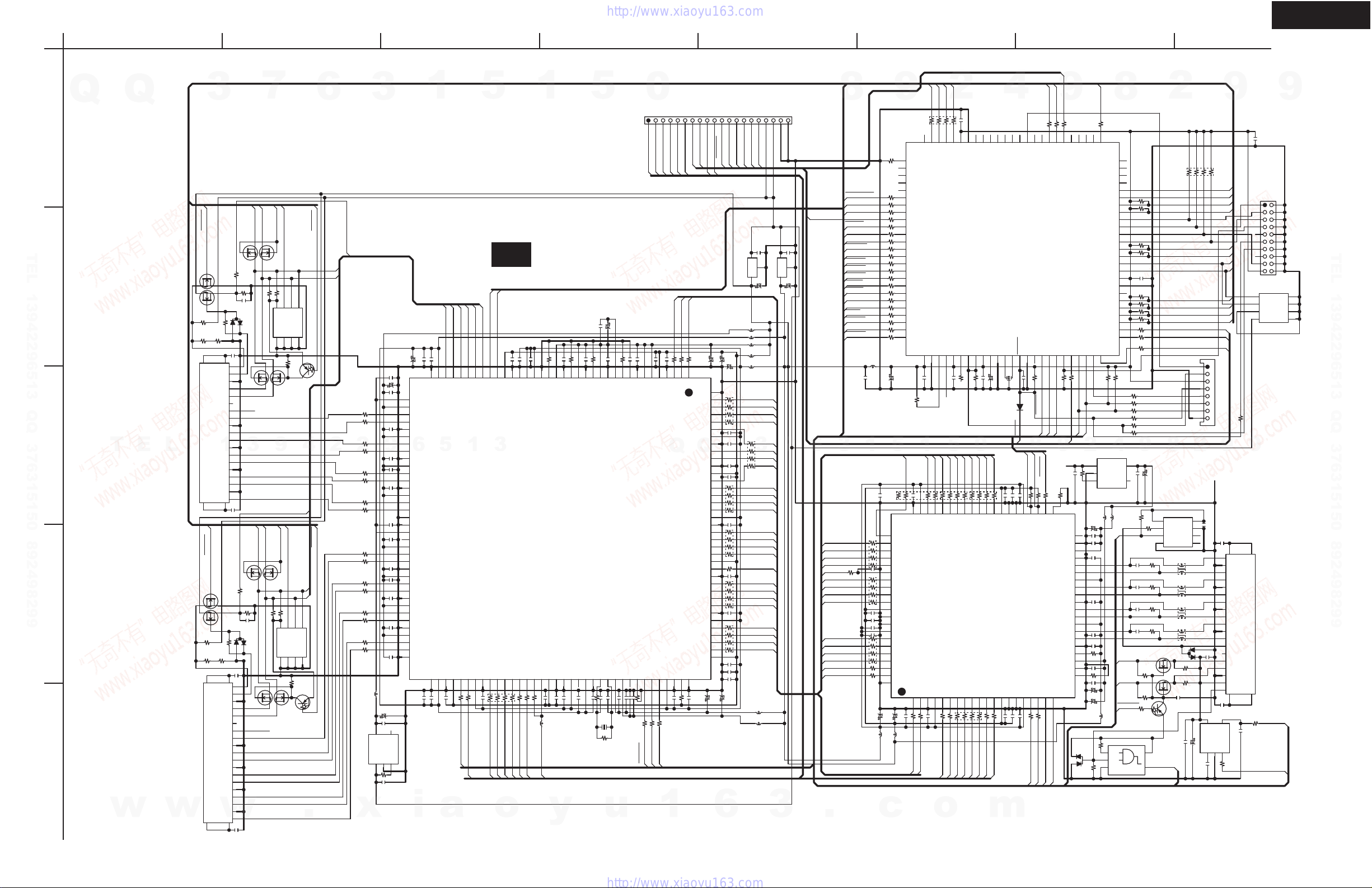
DTR-7.6
A
BCDEFGH
SCHEMATIC DIAGRAM
HDMI section
R0PWR5V
Q8504
UM6K1N
R8536
R8535
C8581
2
1
D8501
19
18
17
16
15
14
13
12
11
10
9
8
7
6
5
4
3
2
1
105Z
Q8604
UM6K1N
R8636
104Z
D8601
1
105Z
19
18
17
16
15
14
13
12
11
10
9
8
7
6
5
4
3
2
1
C8698
21
105Z
5
10K
10K
3
1SS226
5
Q8503
UM6K1N
R0XCN
R0XCP
R0X0P
3
R0X0N
R0X1N
R0X1P
R0X2N
R0X2P
R1PWR5V
5
10K
R8635
10K
C8681
2
3
1SS226
Q8603
UM6K1N
7
SCL_DDC0
4
1
6
3
3.3K
R8542
DSCL0
DSDA0 SDA_DDC0
+3_3VHD1
4
3
CEC
SCL_DDC1
SDA_DDC1
4
1
6
3
3.3K
R8642
DSCL1
DSDA1
4
5
3
CEC
R1XCN
R1XCP
R1X0N
R1X0P
R1X1N
R1X1P
R1X2N
R1X2P
SWEP0
PROEP0
2
3.3K
R8543
6
8
7
WP
VCC
Q8506
A02A13A24GND
1
1
2
6
9
SWEP1
PROEP1
2
R8643
7
8
WP
VCC
Q8606
A02A13A24GND
+3_3VHD1
1
1
2
6
5
SCL
10K
R8544
3.3K
6
SCL
R8644
DTA144EE
6
R0_HPR
SDA
BR24L02FV-W
4
R1_HPR
5
SDA
BR24L02FV-W
10K
Q8607
.
Q8507
DTA144EE
2
0
R8567
0
0
R8569
2
0
R8570
0
R8571
0
R8572
0
R8573
0
0
R8575
0
0
R8577
0
R8578
0
R8579
0
R8580
0
R8581
0
R8582
x
3
PVCC
R8568
R8574
R8576
L8506
BLM21PG221
+3_3VPLL
C8623
105Z
5
VOUT
Q8602
VIN2VSS3CE
XC6213B332M
1
1K
C8622
+5VHD
C8523
C8525
C8528
C8532
C8624
105Z
C8519
102J
C8520
C8521
102J
C8522
102J
102J
9
C8524
105Z
102J
C8526
102J
C8527
102J
102J
C8529
105Z
C8530
102J
C8531
102J
105Z
220/4
R8633
4
NC
Q
Q
3
1
+5VHD
R0_HPR
TEL 13942296513 QQ 376315150 892498299
Q8505
+3_3VHD1
UM6K1N
2
3
T
E
L
4
5
w
w
6
2
1K
R8545
R8538
10K
22
HP DET
Shield
DDC DATA
DDC CLK
CERemote
CK Shield
P8501
D0 Shield
HDMI IN1
D1 Shield
D2 Shield
Val
Shield
23
R1_HPR
+3_3VHD1
6
2
1K
R8645
R8638
10K
22
Shield
DDC DATA
DDC CLK
CERemote
CK Shield
P8601
D0 Shield
HDMI IN2
D1 Shield
Val
D2 Shield
Shield
23
453
1
104Z
R8534
10K
R8541
10K
C8599
105Z
20
+5V
GND
NC
CK-
CK+
D0-
1
D0+
D1-
D1+
D2-
D2+
21
C8598
+5VHD
Q8605
UM6K1N
453
1
R8634
10K
R8641
10K
C8699
20
HP DET
+5V
GND
NC
CK-
CK+
D0-
D0+
D1-
D1+
D2-
w
D2+
22/4
37
38
39
40
41
42
43
44
45
46
47
48
49
50
51
52
53
54
55
56
57
58
59
60
61
62
63
64
65
66
67
68
69
70
71
72
22/4
GND
1
5
1
U01
DSCL0
DSCL1
DSDA0
DSDA1
SCL_RX
31
30
DSCL1
DSDA0
1
102J
R8509
33
HDMISPF
29
DSDA1
C8536
R8511
SDA_RX
28
27
26
CSCL
CSDA
3
33X4
PCMSBLR
PCMCSW
PCMSLR
o
102J
C8515
25
IOVCC
IOGND
PCMLR
105Z
C8513
C8514
24
23
22
CVGND
CVCC18
R8514
R851333R8512
33
33
PCMBCK
PCMLRCK
105Z
75
102J
R8507
21
18
20
19
AnBPb
DACVCCB
DACDGND
DACDVCC18
Q8501
SII9031
HDMI Receiver
C8539
C8537
C8538
102J
L8517
105Z
C8537
BK1608LM182
MCK_HDMI
y
R0PWR5V
R1PWR5V
102J
C8517 105Z
C8518
C8516
33
32
34
35
36
DGND
DSCL0
DVCC18
PVCC0
AVCC
R0XCR0XC+
AGND
AVCC
R0X0+
6
R0X0AGND
AVCC
R0X1R0X1+
AGND
AVCC
R0X2R0X2+
AGND
TMDSPGND
PVCC1
RSVD_A
AVCC
R1XCR1XC+
AGND
AVCC
R1X0R1X0+
AGND
AVCC
R1X1R1X1+
AGND
AVCC
R1X2R1X2+
AGND
105Z
i
R1PWR5V
R0PWR5V
5
DGND74DVCC1875IOGND76IOVCC77MUTEOUT78SPDIF79CVCC80CGND81SD382SD283SD184SD085WS86SCK87MCLKIN88MCLKOUT89IOVCC90IOGND91CGND92CVCC1893NC94AUDPVCC18
73
102J
R8508
C8534
C8535
33
102J
C8533
MUTEOUT
a
R850675C8512
17
16
AnGY
DACGNDB
C8540
102J
105Z
5
+3_3VHD1
MPU
105Z
C8510
102J
75
C8508
C8511
R8505
15
14
13
12
AnRPr
DACVCCR
DACVCCG
DACGNDG
AUDPGND96XTALOUT97XTALIN98XTALVCC99REGVCC
95
C8541
102J
180J
R8516
C8542
X8501
33
R8515
1M
X8501
28.332MHz
u
22/4
330
C8509
105Z
R8504
11
COMP
DACGNDR
180J
C8543
C8544
105Z
0
P8003
123456789
PCMLRCK
PCMBCK
105Z
105Z
105Z
C8505
C8507
C8506
6
8
7
9
VREF10RSET
DACAVCC
DACOVCC
DACAGND
RSVDL
RESET#
SCDT
100NC101
102
103
R8519
R8518
C8546105Z
C8547102J
C8545
R8517
100
100
102J
4.7K
RX_RST
SCDT
PCMCSW
PCMLR
HDM_VSYNC
102J
33
C8504
3
5
4
IOVCC
IOGND
Q
INT
CVCC18
104
105
106
105Z
C8548
R8520
100
INT_RX
1
RXMUTE
PCMSLR
PCMSBLR
HDM_BLNK
HDM_HSYNC
33
R8501
R850233R8503
2
1
DE
VSYNC
HSYNC
CVCC18
CGND
IOGND
IOVCC
CVCC18
CGND
IOVCC
ODCK
IOGND
CGND
CVCC18
IOVCC
CGND
CLK48B
IOGND
107
108
102J
C8549
R8521
10K
1011121314151617181920
VDMRST
VDM_SCK
VDM_SI
VDM_SO
444
C8502
GND
C8551
C8501
22/4
R8528
C8562
C8561
102J
105Z
C8560
C8559
R8526
102J
C8558
R8525
R8524
102J
R8523
C8555
R8522
C8554
C8553
C8552
L8501
22/4
33
22/4
Q8591
BA33BC0FP
BLM21PG221
BLM21PG221
L8502
BLM21PG221
BLM21PG221
BLM21PG221
IOVCC
CVCC18
33X4
105Z
R8527
102J
33X4
33X4
HDM_PIXCLK
C8556
33X4
102J
33X4
105Z
102J
105Z
BLM21PG221
BLM21PG221
VDM_STB
+5VHD
1
3
+3_3VHD1
L8505
HDM_CB2
HDM_CB3
HDM_CB4
HDM_CB5
HDM_Y6
HDM_Y7
HDM_Y8
HDM_Y9
HDM_CR2
HDM_CR3
HDM_CR4
HDM_CR5
HDM_CR6
HDM_CR7
HDM_CR8
HDM_CR9
HDMISPF
TXMUTE
DVCC
22/4
ePAD
Q0
Q1
Q2
Q3
Q4
Q
Q5
Q6
Q7
Q8
Q9
Q10
Q11
Q12
Q13
Q14
Q15
Q16
Q17
Q18
Q19
Q20
Q21
Q22
Q23
C8550
MCK_HDMI
C8503
145
144
143
142
141
140
139
138
137
136
135
134
133
132
131
130
129
128
127
126
125
124
123
122
121
120
119
118
117
116
115
114
113
112
111
110
109
22/4
6
+10S
C8591
105Z
I
2
G
O
C8592
100/4
L8503
L8504
HDM_CB6
HDM_CB7
3
HDM_CB8
HDM_CB9
33X4
HDM_Y2
HDM_Y3
HDM_Y4
HDM_Y5
L8508
L8507
+5VHD
+5VHD
Q8592
BA18BC0FP
3
GND
GND
C8593
+5VHD
105Z
1
I
2
G
O
3
100/4
C8594
7
+1_8VHD2
+3_3VHD1
6
HDM_Y6
HDM_Y5
HDM_Y4
HDM_Y3
HDM_PIXCLK
HDM_Y2
HDM_CB9
HDM_CB8
HDM_CB7
HDM_CB6
HDM_CB5
HDM_CB4
HDM_CB3
HDM_CB2
HDM_BLNK
.
8
DVDA_ENH
PASS_ANA
PASS_HDM
RXMUTE
INT_VD
RTC
HDMI_POW
DVIHDMI
TEST0
RX_RST
R0_HPR
R1_HPR
VDOFF
IP_RST
HPLG_TX
HPLGDET
HDOE
VE_RST
SCDT
VD_RST
3
R8421
22X4
100D
R8422
22X4
105Z
C8424
102J
C8425
105Z
C8426
102J
C8427
22X4
22
22
22
22
22
22
22
22
22
22
22
22
22
22
22
22
22
22
22
22
0
22
L8701
4.7U
105Z
C8708
1
102J
C8428
R8423
R8424
R8425
R8426
22/4
BLM21PG221
+1_8VHD2
c
2
SWEP0
SWEP1
PROEP0
PROEP1
22X4
75
R8737
DB3
74
DB1
DB2
72
73
PDL2/AD2
PDL3/AD3
PDL4/AD4
C8707
DB0
71
70
BVDD
PDL0/AD0
PDL1/AD1
105Z
69
BVSS
66
68
67
PCT4/_RD
PCT6/ASTB
PCT1/_WR1
MPD70F3261YGC-8EA
AVREF02 AVSS03 P10/ANO04 P11/ANO15 AVREF16 PDH4/A207 PDH5/A218 FLMD09 VDD0
1
105Z
105Z
C8702
C8701
MODE1
MODE0
4.7K
5
1
R8416,R8417:22X4
HDM_Y8
HDM_Y9
105Z
HDM_CR3
HDM_CR2
HDM_CR4
59
CGND
CVCC18
HDMI Transmitter
HSYNC2VSYNC3CGND4CVCC185SPDIF6MCLK7SD38SD29SD110SD011WS12SCK13IOVCC14IOGND15CGND16CVCC1817INT18HPD19DSDA20DSCL
C8404
R840222R8401
102J
22
HDMISPF
MCK_HDMI
R840422R8403
PCMSBLR
22
HDM_VSYNC
o
10
R8706
C8704
R8705
C8703
1K
10K
105Z
CSTCR5M00G53-B0
0
HDM_CR7
HDM_CR6
HDM_CR5
HDM_CR8
R8417
SII9030
Q8401
R8405
22X4
PCMLR
PCMLRCK
PCMSLR
PCMCSW
m
REGC
HDM_CR9
49
R8406
22
PCMBCK
R8738
47K
R8739
R8758
R8757
R8756
R8755
R8754
R8740
R8741
R8752
R8747
R8748
R8749
R8750
R8751
R8742
R8743
R8753
R8744
R8745
R8746
C8709
C8423
61
62
63
64
65
66
67
68
69
70
71
72
73
74
75
76
77
78
79
80
81
C8401
L8401
0
9
76
77
78
79
80
81
82
83
84
85
86
87
88
89
90
91
92
93
94
95
96
97
98
99
100
220/4
5
HDM_Y7
22x4
R8418
D13
D12
D11
D10
D9
IDCK
D8
D7
D6
D5
IOVCC
IOGND
CGND
CVCC18
D4
D3
D2
D1
D0
DE
ePAD
22/4
C8402
105Z
L8402
+3_3VHD1
PDL5/FLMD1
PDL6/AD6
PDL7/AD7
PDL8/AD8
PDL9/AD9
PDL10/AD10
PDL11/AD11
PDL12/AD12
PDL13/AD13
PDL14/AD14
PDL15/AD15
PDH0/A16
PDH1/A17
P711/ANI11
P710/ANI10
P79/ANI9
P78/ANI8
P77/ANI7
P76/ANI6
P75/ANI5
P74/ANI4
P73/ANI3
P72/ANI2
P71/ANI1
P70/ANI0
R8701
C8422
60
1
C8403
HDM_HSYNC
4
63
65
64
PCT0/_WRO
PCM2/_HLDAK
PCM3/_HLDRQ
Q8701
VSS0
11
12 X113 X214
4.7/50
X8701
D8701
102J
102J
105Z
C8421
C8420
R8416
46
47
48
D2350D2251D2152D2053D1954D1855D1756D1657D1558D14
IOVCC
IOGND
R8407
C8405
22
102J
105Z
62
59
61
60
PHD3/A19
PCM0/_WAIT
PCM1/CLKOUT
RESET
XT1
XT2
15
16
17
10K
R8707
C8705
105Z
TX_RST
1SS355
VDMRST
8
SCL_TX
SDA_TX
C8419
4.7k
R8415
44
43
45
CSCL
CSDA
CGND
CVCC18
R8408
C8406
C8407
22
22
102J
HPLG_TX
INT_TX
9
INT_VS
TXMUTE
22
MUTEOUT
22
R8732
R8731
R8730
57
58
56
PDH12/A18
P914/INTP5
P915/INTP6
P02/NMI
P04/INTP0
P04/INTP1
18
19
20
10K
R8710
DRST
INT_TX
INT_RX
9
+5VHD
TX_RST
4.7k
4.7k
R8413
R8414
41
42
CI2CA
RESET#
PGND2
PVCC2
AGND
TX2+
TX2-
AVCC
TX1+
TX1-
AGND
TX0+
TX0-
AVCC
TXC+
TXC-
AGND
EXT_SWING
PVCC1
PGND1
RSVDL
R8409
SDA_ODDC
SCL_ODDC
22
55
53
54
P911/SOB3
P913/INTP4
P912/_SCKB3
P05/INTP2/_
P06/INTP3
PP40/SDA01
21
22
23
22
R8709
SCL_TX
SDA_TX
VDM_STB
2
1K
R8452
C8451
105Z
4.7k
R8411
40
NC
39
38
37
36
35
34
33
32
31
30
29
28
27
26
25
24
23
22
21
GND
C8408
22/4
1SS226
3
1
2
D8301
CEC_IO
22
R8729
52
51
P98/SOB1
P910/SIB3
P99/SCKB1
P97/SIB1
P96/A6
P95/A5
P94/A4
P93/A3
P92/A2
P91/SCL02
P90/SDA02
P55/DMS
P54/DCK
P53/DDO
P52/DDI
P39/SCL00
P38/SDA00
EVDD
EVSS
P32/ASCKA0
P31/RXDA0
P41/SCL01
P42
P30TXDA0
24
25
2.2K
R8712
Q8404
XC6213B332M
1
VIN
2
VSS
3
CE4NC
BLM21PG221
L8404
C8418
C8417
22/4
C8416
105Z
102J
C8415
102J
C8414
105Z
C8413
102J
C8412
R8410
105Z
470
C8411
102J
R8427
4.7K
C8410
105Z
C8409
22/4
L8403
Q8306
4.7K
1
R8324
2
3
47K
R8325
8
50
49
48
47
2.2K
46
R8727
45
44
43
R8726
42
2.2K
41
2.2K
40
R8734
39
38
P51
37
P50
R8733
36
2.2k
35
C8706
34
105Z
33
32
P37
31
P36
30
P35
P34
29
P33
28
R8721
27
R8720
26
R8719
22
2.2K
R8711
GND
R8713
R8714
R8715
R8716
R8717
R8718
9
4
105Z
5
VOUT
C8452
R8462
L8405
CEC
BLM21PG221
CEC_IO
104K
C8304
104K
C8303
104K
C8302
104K
C8301
SCL_ODDC
4.7K
R8337
SDA_ODDC
R8338
4.7K
DVIHDMI
1K
R8333
BLM21PG221
TX_HPLG
+3_3VHD1
TC7SZ08FU
VCC
INA
INB
OUTY
GND
2
SCL_ODDC
SDA_ODDC
SCL_DDC1
SDA_DDC1
OC_DMS
OC_DCK
OC_DDO
OC_DDI
R8725
R8724
R8723
R8722
22
22
HS
FWVDD
22
FWSCK
22
FWSO
22
FWSI
FWRESET
22
0
FWFLMD0
0
8
C8453
220/4
GND
+3_3VHD1
SN74CB3Q3305PWR
27K
1
1OE
R8461
2
1A
0
3
1B
4
GND52A
ACM2012D-900-2P
330
R8304
ACM2012D-900-2P
330
R8303
ACM2012D-900-2P
330
R8302
ACM2012D-900-2P
330
R8301
CEC
1SS226
UM6K1N
1
6
4
3
5 2
C8330
DTA144EE
5
HPLGDET
4
SCL_DDC0
SDA_DDC0
SCL_VDVE
SDA_VDVE
2.2K
2.2K
2.2K
2.2K
VDM_SCK
P8702
OC_FLMDO
VCC
2OE
2B
Q8461
1234
L8409
1234
L8408
1234
L8407
3
2
4 1
2
D8461
R8334
2.2K
R8335
Q8309
2.2K
105Z
Q8308
105Z
C8329
C8328
R8728
10KX4
SCL_RX
SDA_RX
SCL_IP
SDA_IP
VDM_SI
VDM_SO
1
2
3
4
5
6
7
8
2
8
7
6
TX2+
TX2TX1+
TX1TX0+
TX0TXC+
TXC-
L8406
1
C8332
3
105Z
22/16
C8327
4
105Z
105Z
VO
GND
C8461
C8398
C8399
9
FLASHWRITER
9
P8302
105Z
21
1
D2+
2
D2 Shield
3
D2-
4
D1+
5
D1 Shield
6
D1-
7
D0+
8
D0 Shield
9
D0-
10
CK+
11
CK Shield
12
CK-
13
CERemote
14
NC
15
DDC CLK
16
DDC DATA
17
GND
18
+5V
19
HP DET
20
105Z
5
VIN
CONT2GND3BYP
1
NJM2860F3-05
10K
R8323
C8710
1
2
3
4
5
6
7
8
9
10 20
BR24L08FV-W
5
6
7
8
+5VHD
OC_SYSRST
R87080
9
Val
23
Shield
Shield
22
R8341
10
105Z
C8326
Q8305
HDMI_POW
9
105Z
P8703
11
12
13
14
15
16
17
18
19
4
SDA
GND
3
SCL
A2
2
WP
A1
VCC1A0
Q8702
HDMI OUT
+10S
TEL 13942296513 QQ 376315150 892498299
Page 19
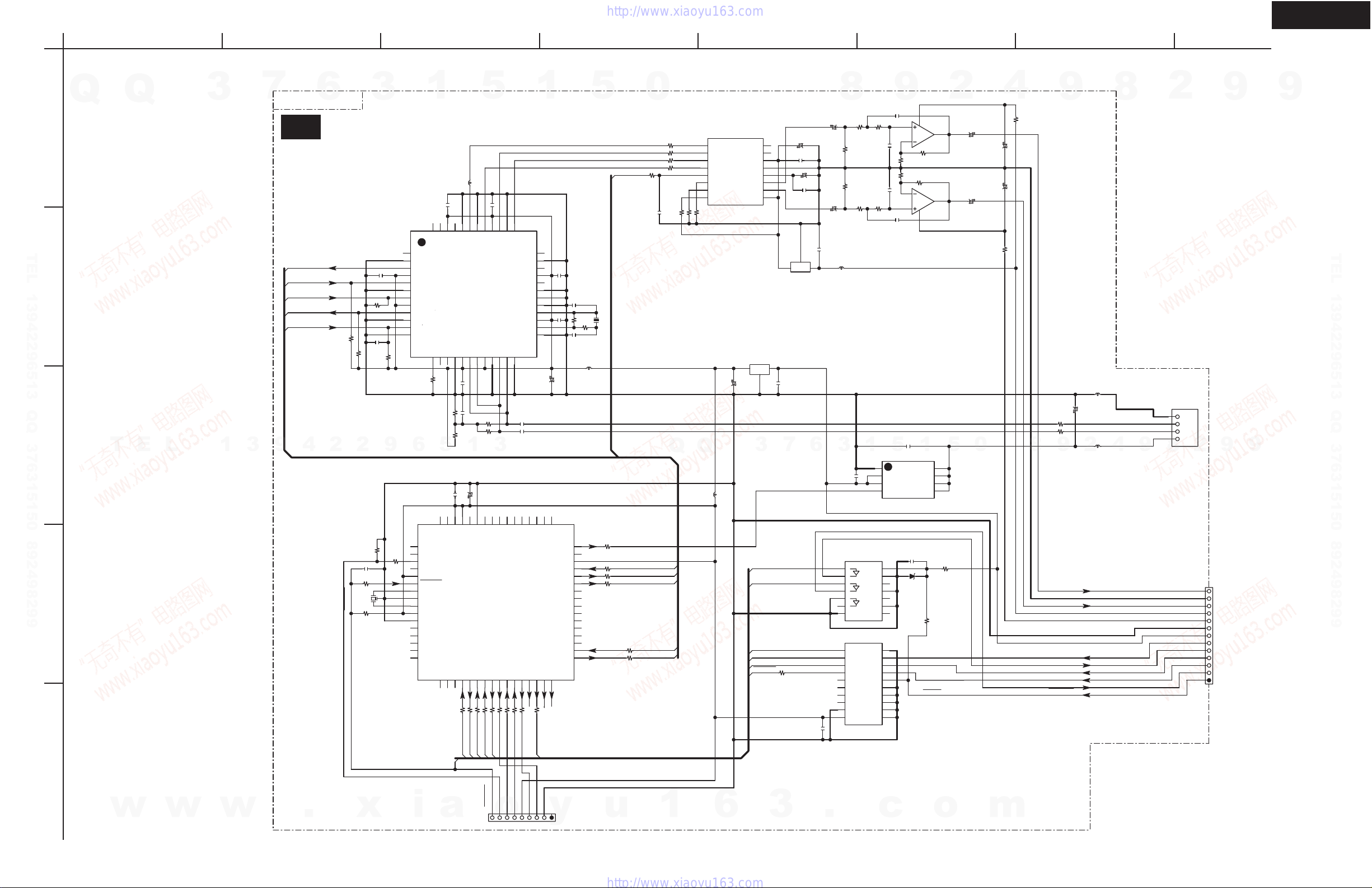
DTR-7.6
A
BCDEFGH
SCHEMATIC DIAGRAM 11
XM RADIO SECTION (North American models)
Q
Q
3
1
TEL 13942296513 QQ 376315150 892498299
2
3
T
E
L
1
7
3
NARF-8688
6
U08
XMSDI_L
XMSDO_L
XM_COM_SEL
XM_ERR_IRQ
XM_RESET
9
4
2
100K
R7101
R7103
100K
2
3
C7101
104Z
R7102
100K
C7102
102K
R7104
9
1
LSDP
2
VSS
3
SC_TX_OUT
4
VDD
5
SC_RX_IN
6
VSS
7
CMD_SEL
8
VDD
9
ERR_IRQ
10
VSS
11
RST
12
100K
6
1
104Z
C7118
46
47
48
SAII_EN
SAII_DA
COMM_RX_DIG
COMM_TX_DIG
13
14
15
100K
R7105
R7111
R7112
5
C7002
63
5
L7103
BK1608LM182
C7116
41
42
43
44
45
VDD
VSS
VSS
SAII_CLK
I2S_OCLK
Q7101
XMDTIC
F2602-01
12 SLAVE_SEL
COMM_TX_EN
VSS17VDD18COMM_RX_P
COMM_RX_M
16
19
20
104Z
C7103
104Z
100
1K
C7104
R7113
1K
R7114
100
1
104Z
C7003
58
59
61
60
62
I2S_OCLK
I2S_SCLK
I2S_SDO
I2S_LRCLK
104Z
37
38
39
40
VSS
VDD
I2S_DA
I2S_CLK
HSDP_EN
I2S_LRCLK
VDD21VSS22COMM_TX_M
100/16
57
3
56
VSS
HSDP_CLK
VDD
HSDP_DA
VSS
TEST
VSS
OSC_IN
VDD
OSC_OUT
VSS
COMM_TX_P
VSS
23
24
C7105
104Z
C7106
104Z
53
54
55
1
36
35
34
33
32
31
30
29
28
27
26
25
52
C7114
C7111
49
C7115
104Z
C7113
C7112
104Z
040C
100/16
080D
R7116
1M
R7115
680
L7105
022K
5
DAC_RESET
X7101
45.1584MHz
0
R7117
R7118
R7119
R7120
R7121
+3.3VVDD
102K
C7119
Q
100
330
330
330
0
R71270R7128
R71260
1
MCLK
2
BICK
3
SDTI
4
LRCK
5
PDN
6
SMUTE/CSN
7
ACKS/CCLK
8
DIF0/CDTI9P/S
0
Q
L7001
Q7102
VCOM
AK4384ET
AOUTL
AOUTR
TA48033AF
C7007
470/6.3
022K
16
DZFL
15
DZFR
14
VDD
13
VSS
12
11
10
Q7004
3
O
I
G
2
3
XM_PWR_CTRL
1
C7121
1
C7006
7
C7123
470/6.3
C7122
104Z
C7120
104Z
O3I
Q7105
78L05
104Z
10/50
2
G
6
C7125
10/50
C7137
C7124
10/50
104Z
L7104
022K
3
8
R7130
2.2K
R7142
100K
100K
R7143
R7131
2.2K
C7134
104Z
R7132
R7133
1
C7128
2.2K
821J
C7126
821J
C7127
2.2K
1
2
IN
3
IN
4
EN
TPS2011AD
9
821J
C7129
821J
C7135
5
104Z
GND
Q7104
3
Q7103
2
R7134
3.3K
R7135
R7137
6
Q7103
5
8
R7136
4
OUT
OUT
OUT
OUT
2
NE5532APSR
1
2.2K
3.3K
2.2K
7
NE5532APSR
5
1
8
7
6
5
C7130
10/50
C7131
10/50
0
R_OUT
4
R7138
C7132
C7133
100/16
22
R7139
22
L_OUT
100/16
8
R7141
22
R7140
22
9
9
8
L7102
BLM21PG221SN1
C7136
100/16
L7101
4
2
BLM21PG221SN1
9
2
4
3
2
1
8
P7102
GND
D+
D-
+V
2
9
9
9
TEL 13942296513 QQ 376315150 892498299
9
P9364P92
P100
AVSS
VREF
1
P91
1K
R7001
2
3
4
5
6
7
8
9
10
11
12
13
14
15
16
P90
CNVSS
P87
P86
RESET
XOUT
VSS
XIN
VCC
P85
P84
P83
P82
P81
P80
10K
R7002
C7001
104Z
R7003
1K
4
RESET
CNVSS
X7001
20MHz
R7033
10K
5
w
w
w
.
x
i
AVCC
M30281FAHP
P7718P7619P7520P7421P7322P7223P7124P7025P6726P6627P6528P6429P3330P3231P3132P30
17
1K
1K
1K
R7005
R7006
R7007
MSREQ
MCLK
MHREQ
a
P103
P102
P101
Q7001
220
1K
1K
R7008
R7009
R7010
MSDI
MSDO
CNVSS
RESET
o
P105
P104
220
220
R7011
R7012
FW_RXD
FW_SCLK
P107
P106
220
R7013
DAC_RESET
VCC
FW_TXD
FW_BUSY
1K
R7014
GND
y
P0250P0151P00
P03
P15
P16
P17
P20
P21
P22
P23
P24
P25
P26
P27
P60
P61
P62
P63
P7001A
123456789
R7024
1K
R7023
R7022
R7021
1K
u
XM_PWR_CTRL
XM_ERR_IRQ
1K
1K
XM_RESET
XM_COM_SEL
R7018
220
XMSDI_L
XMSDO_L
R7017
220
1
6
MSDO
MSREQ
MSDI
MCLK
MHREQ
RESET
R7004
10K
3
Q7003
TC74HCT7007AF
1
2
3
4
5
6
7
GND8OUT4
11
Y8
12
Y7
13
Y6
14
Y5
15
Y4
16
Y3
17
Y2
18
Y1
19
_G2
20
VCC1_G1
104Z
C7004
.
14
VCC
13
IN6
12
OUT6
11
IN5
10
OUT5
9
IN4
10
GND
9
A8
8
Q7002
A7
7
A6
6
A5
5
A4
4
A3
3
A2
2
A1
TC74VHC541FT
c
C7005
104Z
D7001
R7025
220
UDZS5.1B
10K
R7032
XMSDO
XMCLK
XMREQ1
XMRST
o
m
L_OUT
AGND
R_OUT
+12V
-12V
GND
+5V
XMSDO
XMSDI
XMCLK
XMREQ1
XMREQ2
XMRST
13
12
11
10
9
8
7
6
5
4
3
2
1
P710B
48
47
46
45
44
43
42
41
40
39
38
37
36
35
34
33
Page 20
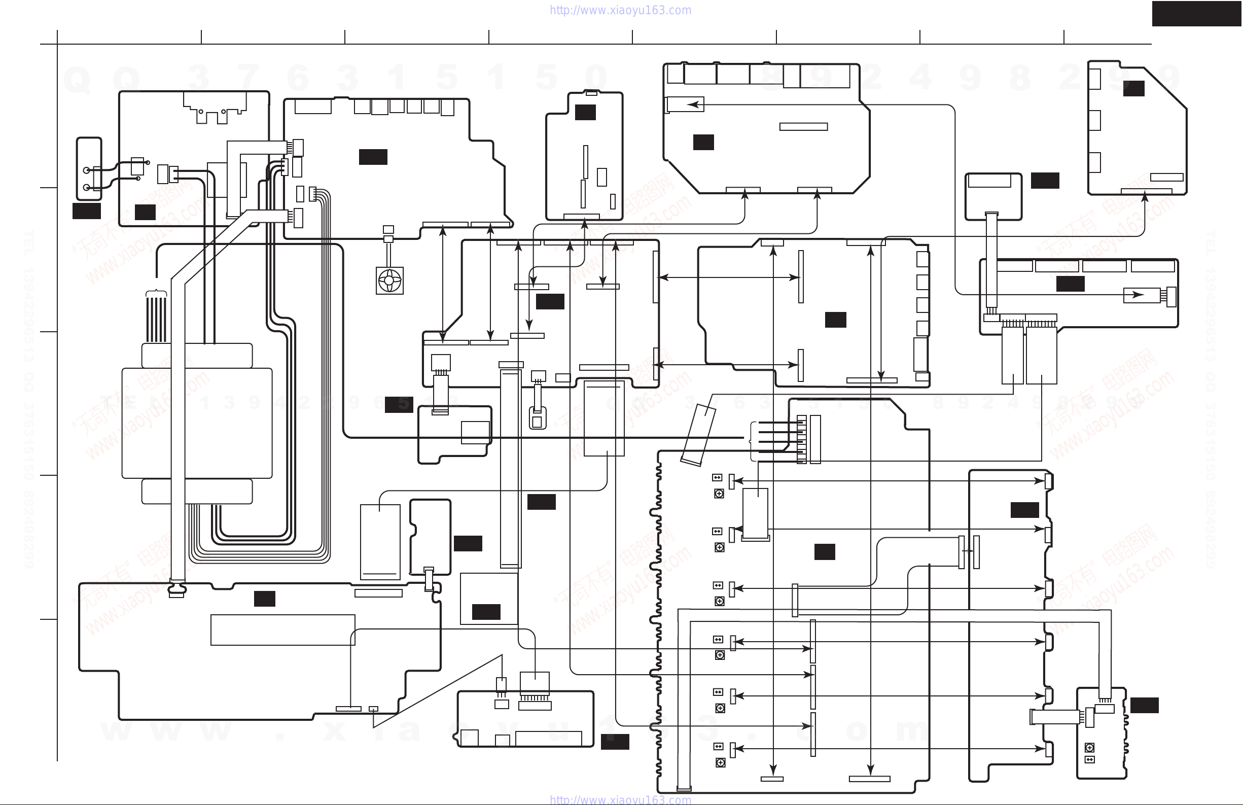
DTR-7.6
A
BCDEFGH
PRINTED CIRCUIT BOARD CONNECTION DIAGRAM
P912
Sch. 7
JL957A
3
P910
P905A
Power
1
transformer
Sch. 7
Q
1
P907B
NAETC-8671
P906B
U047
TEL 13942296513 QQ 376315150 892498299
AC inlet
Sch. 7
2
3
4
P908
T
Q
NAPS-8664
Primary
circuit
P901A
P906A
E
P907A
U04
To P6952A
L
T902
3
7
P904A
JL911A
9
U07
4
6
JL957B
2
P5501
JL911B
P951
P952
2
3
P5502
9
Headphone
terminal
P7534B
P5503
U042
P955
6
Sch. 9
1
P5505
P5506
Secondary circuit
FAN
U073
5
5
P5507
P5504
NAPS-8665
Sch. 8
P959B
P959A
1
JL7542B
NAETC8685
NAETC-8687
JL7503B
JL7503A
3
P954B
P954A
JL7452A
P7602
U075
Volume
Sch. 9
TUNER
PACK
U011
1
P3105B
P701A
5
Sch. 11
P7101A
P710B
P3104B
P2005A
U032
P710A
JL703B
JL703A
Thermal
detector
Sch. 5
U062
NAETC8680
XM radio
North American
models
0
P7102
U08
NARF-8688
P7005A
JL101B
P7001A
P3103B
P2004A
NAAR8661
Main
microprocessor
P7534A
P702
Sch. 3
Q
P602B
Q
P601B
P2003
P2007
Video circuit
JL2006
U02
3
P6080
R6040
P6081
R6041
P6082
R6042
7
JL6600A
P6001A
P6083
P2002
NAVD-8657
Sch. 1
P2005
P3102B
NADG-8660
6
P6000A
JL6603A
P6002A
P6003A
P2001
8
3
P2202
P2305A
P2004
5
1
Amplifier
Sch. 4 & 5
NAAF-8678
P5004B
P2201
9
P602A
Sch. 2
P601A
P6952A
U06
P3105A
P3101B
U03
DSP
1
P801A
2
5
0
4
P101
P102
P6602
2
NAAF8668
Sch. 6
8
NAETC-
8667
NAETC-8666
JL6600B
4
P6000A
U045
P6001A
P6002A
9
JL6602A
JL6602B
U101 U102 U103 U104 U105
9
8
P5004A
2
U044
Speaker
terminal C
Sch. 7
P6600
JL6603B
9
U043
8
Driver
circuit
9
P8501
P8601
P8302
Sch. 7
Speaker terminal
2
U01
HDMI
video
circuit
NAVD-8655
9
Sch. 10
P8003
P6607P6605
JL2006B
9
9
P8703
TEL 13942296513 QQ 376315150 892498299
NADIS-8683
Display circuit
5
w
w
w
Sch. 9
.
JL7504A
x
i
JL7501A
a
o
Front video
U7641
P7601
JL7501B
y
JL7540B
u
Sch. 9
NAETC-
8684
P7631
1
U072
6
R6043
P6084
R6044
P6085
3
R6045
JL6200A
P6004A
P6005A
.
P3102A
c
P3104A
P3103A
o
m
P3101A
P6003A
P6004A
JL6006A
P6005A
R6046
JL6200B
JL6006B
NAAF-8682
P6086
U064
Surround
back
amplifier
Sch. 5
Page 21
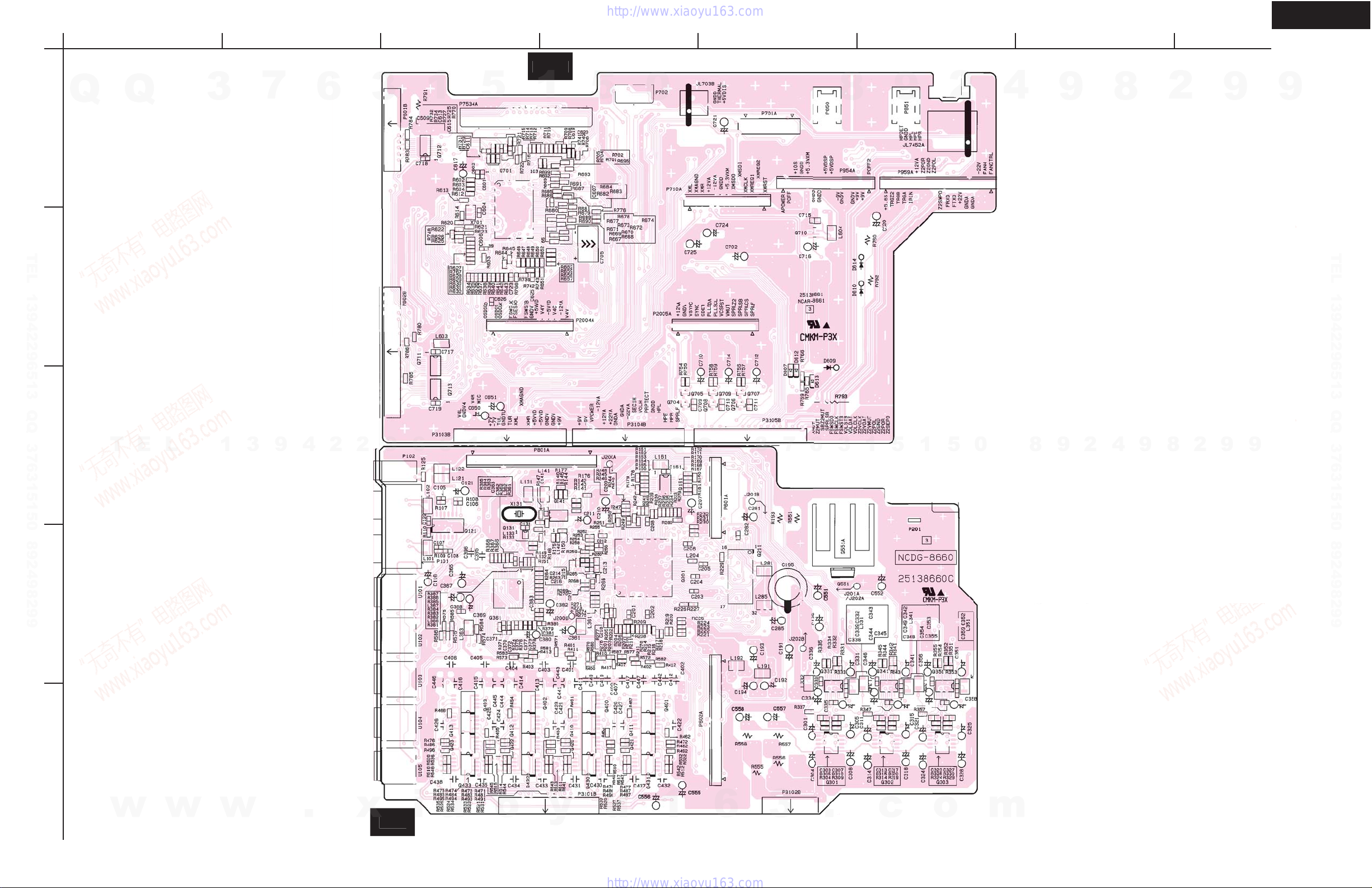
d
DTR-7.6
A
PRINTED CIRCUIT BOARD VIEW
DIGITAL AND MAIN MICRO-
Q
PROCESSOR PC BOARD
1
TEL 13942296513 QQ 376315150 892498299
2
Q
3
7
BCDEFGH
6
3
1
5
1
5
NADG-8660, DSP circuit PC board
0
8
9
2
4
9
8
2
9
9
TEL 13942296513 QQ 376315150 892498299
3
4
5
T
E
L
1
3
9
4
2
2
9
6
5
1
3
Q
Q
3
7
6
3
1
5
1
5
0
8
9
2
9
2
8
9
4
U033
NAETC-8662,
Front video PC board
9
w
w
w
.
x
U03
i
a
o
y
NAAR-8661,Main micropocessor PC boar
u
1
6
3
.
c
o
m
Page 22
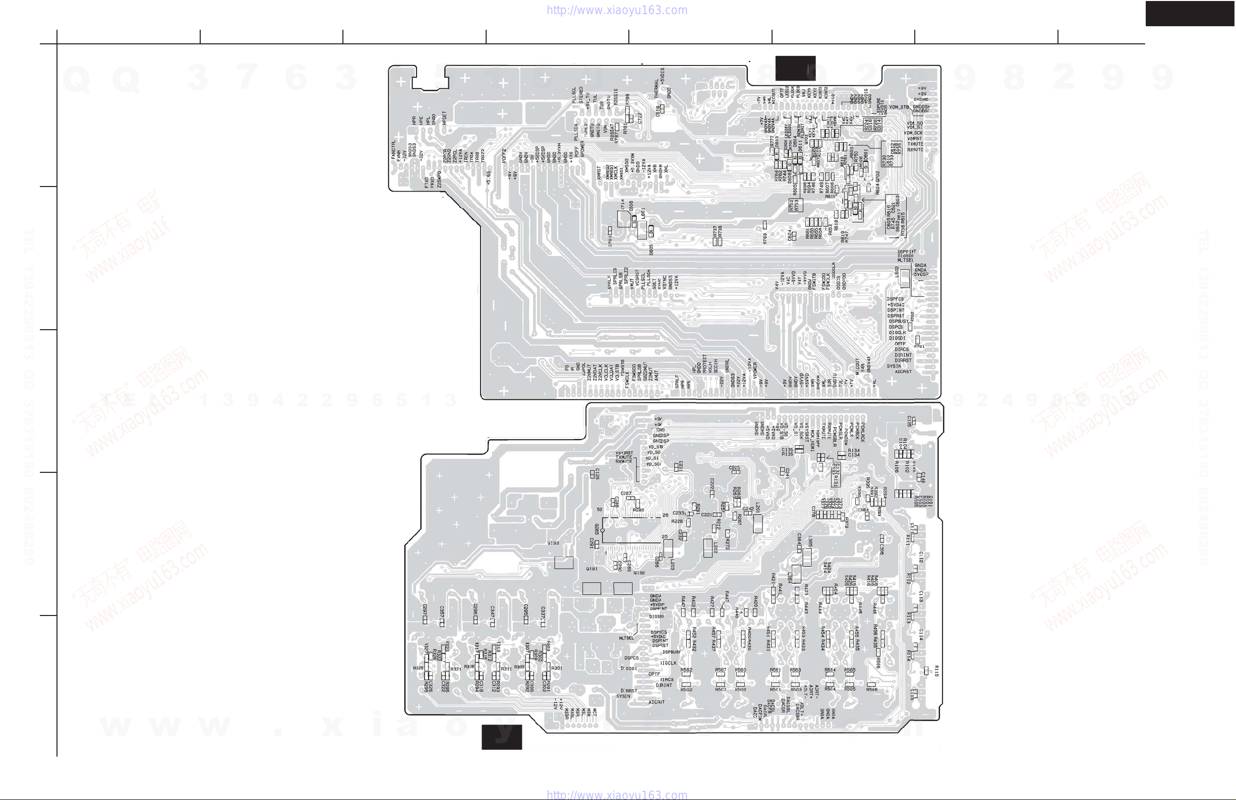
d
,p
DTR-7.6
A
PRINTED CIRCUIT BOARD VIEW
DIGITAL AND MAIN MICRO-
Q
PROCESSOR PC BOARD
1
TEL 13942296513 QQ 376315150 892498299
2
Q
3
7
BCDEFGH
6
U033
3
1
5
1
5
0
8
9
2
4
9
8
2
9
9
TEL 13942296513 QQ 376315150 892498299
3
4
5
T
E
L
1
3
9
4
2
2
9
6
5
1
3
Q
Q
3
7
6
3
1
5
1
5
0
8
9
2
4
9
8
2
9
9
w
w
w
.
x
i
a
o
y
u
NADG-8660, DSP circuit PC boar
1
6
3
.
c
o
m
Page 23
w
d
DTR-7.6
A
PRINTED CIRCUIT BOARD VIEW
AMPLIFIER SECTION
Q
PC BOARD
1
TEL 13942296513 QQ 376315150 892498299
2
Q
3
7
BCDEFGH
6
3
1
5
1
5
0
8
9
2
4
9
8
2
9
9
TEL 13942296513 QQ 376315150 892498299
3
4
5
T
E
L
1
3
9
4
2
2
9
6
5
1
3
Q
Q
3
7
6
3
1
5
1
5
0
8
9
2
4
9
8
2
9
9
U06
w
NAAF-8678,Po
w
w
er amplifier PC boar
.
x
i
a
o
y
u
1
6
3
.
c
o
m
Page 24
DTR-7.6
A
PRINTED CIRCUIT BOARD VIEW
DISPLAY CIRCUIT PC BOARD
Q
1
TEL 13942296513 QQ 376315150 892498299
2
Q
3
7
BCDEFGH
6
3
1
5
1
5
0
U072
NAETC-8684,
Front video PC board
U073
NAETC-8685,
Headphone terminal
8
PC board
9
2
4
U075
NAETC-8687,
Volume PC board
9
8
2
9
9
TEL 13942296513 QQ 376315150 892498299
3
4
5
T
E
L
1
3
9
4
2
2
9
6
5
1
3
Q
Q
3
7
6
3
1
5
1
5
0
8
9
2
9
9
2
8
9
4
U07
NADIS-8683,
Display circuit PC board
w
w
w
.
x
i
a
o
y
u
1
6
3
.
c
o
m
Page 25
,
C
,
board
,
Volume PC board
BOARD VIEW
D
,
l
d
2
3
5
DTR-7.6
A
DISPLAY CIRCUIT P BOAR
Q
1
TEL 13942296513 QQ 376315150 892498299
2
Q
3
7
BCDEFGH
6
3
7
NAETC-8687
1
NAETC-8685
5
7
Headphone termina
PC boar
1
5
NAETC-8684
0
7
PC
8
9
2
4
9
8
2
9
9
TEL 13942296513 QQ 376315150 892498299
3
4
5
T
E
L
1
3
9
4
2
2
9
6
5
1
3
Q
Q
3
7
6
3
1
5
1
5
0
8
9
4
2
NADIS-8683
9
8
2
9
boardDisplay circuit P
9
w
w
w
.
x
i
a
o
y
u
1
6
3
.
c
o
m
Page 26
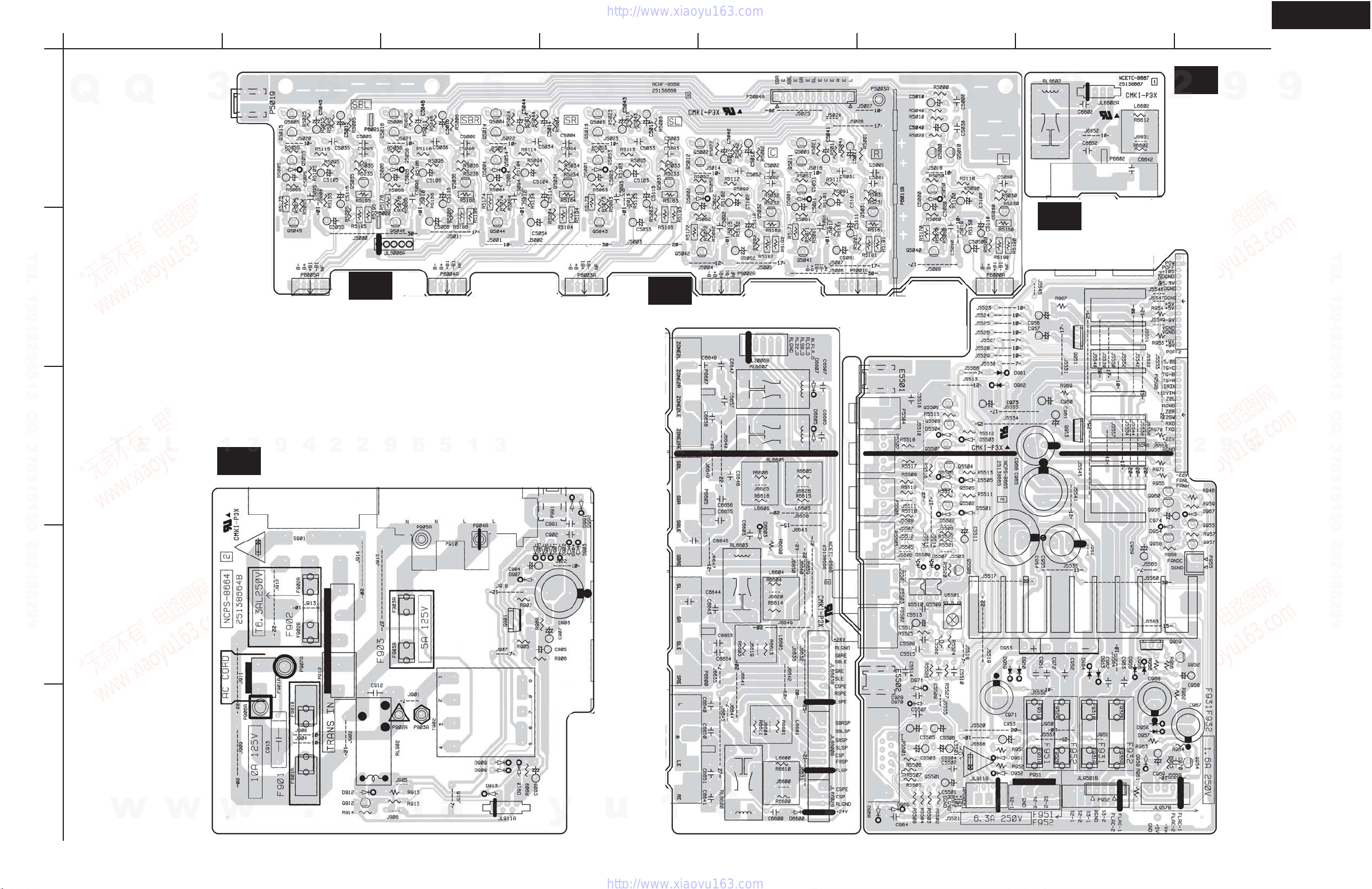
12
DTR-7.6
A
PRINTED CIRCUIT BOARD VIEW
Power supply and
Q
Driver sections
1
TEL 13942296513 QQ 376315150 892498299
2
Q
3
7
BCDEFGH
6
3
U045
NAAF-8668, Driver circuit PC board
1
5
1
5
0
U043
NAETC-8666, Speaker terminal PC board
8
9
2
4
9
U042
NAPS-8665, Secondary
circuit PC board
8
U044
2
NAETC-8667,
Speaker terminal C
PC board
9
9
TEL 13942296513 QQ 376315150 892498299
NASW-8669,
Power switch
PC board
3
4
T
E
L
1
U04
3
9
4
2
2
9
6
5
1
NAPS-8664, Primary circuit PC board
3
Q
Q
3
7
6
3
1
5
1
5
0
8
9
2
4
9
8
2
9
9
5
w
w
w
.
x
i
a
o
y
u
1
6
3
.
c
o
m
Page 27
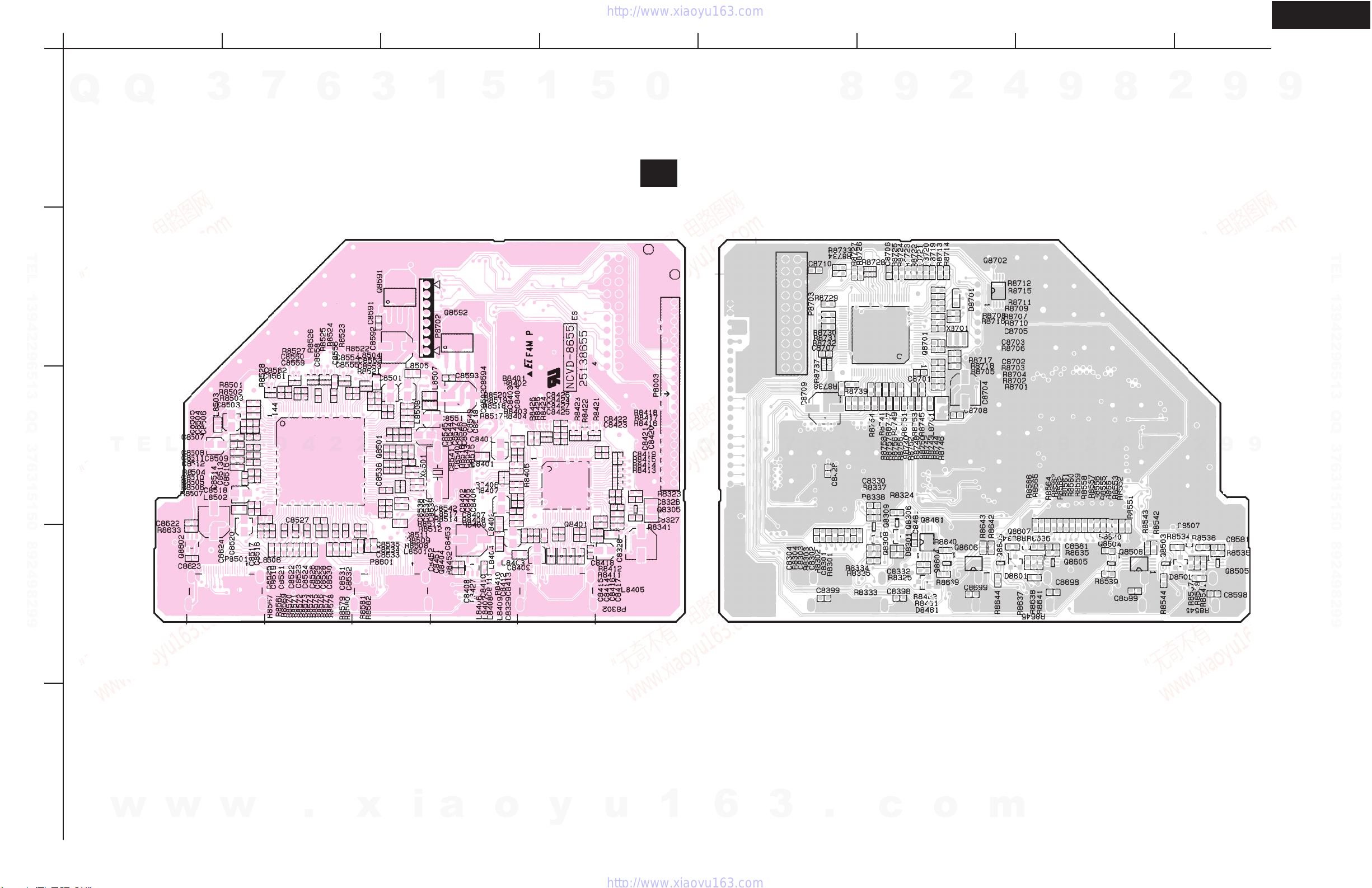
DTR-7.6
A
PRINTED CIRCUIT BOARD VIEW
HDMI CIRCUIT PC BOARD
Q
1
TEL 13942296513 QQ 376315150 892498299
2
Q
3
7
BCDEFGH
6
3
1
5
1
5
NAVD-8655,HDMI circuit PC board
0
U01
8
9
2
4
9
8
2
9
9
TEL 13942296513 QQ 376315150 892498299
3
4
5
T
E
L
1
3
9
4
2
2
9
6
5
1
3
Q
Q
3
7
6
3
1
5
1
5
0
8
9
2
4
9
8
2
9
9
w
w
w
.
x
i
a
o
y
u
1
6
3
.
c
o
m
Page 28

Q
IC BLOCK DIAGRAMS AND DESCRIPTIONS
ADV7172 (Digital PAL/NTSC Video Encoder with Six DACs (10-Bits))
7
Q
3
BLOCK DIAGRAM
6
3
1
5
1
5
0
8
9
2
4
9
8
DTR-7.6
2
9
9
CLOCK
48
14
HSYNC
FIELD/
15
VSYNC
16
TEL 13942296513 QQ 376315150 892498299
BLANK
RESET
TTX
TTXREQ
P0-P7
(COLOR
DATA)
TEL
44
41
INSERTION BLOCK
40
4:2:2 TO
2
4:4:4
|
INTER-
9
POLATOR
13942296513
PAL_NTSC
43
VIDEO TIMING
GENERATOR
TELETEXT
8 8
VCrCb
TO
8
YUV
MATRIX
8
CSO_HSO45VSO14CLAMP
10
BRIGHTNESS AND
CONTRAST CONTROL
Y
U
8
8V
ADD SYNC
INTERPOLATOR
SATURATION CONTROL
ADD BURST
INTERPOLATOR
SCLOCK21SDATA
20
2
I C MPU PORT
10
10
10
REAL-TIME
CONTROL CIRCUIT
39
SCRESET/RTC
Q
Q
ALSB
17
LUMA
PROGRAMMABLE
FILTER
SHARPNESS
FILTER
PROGRAMMABLE
CHROMA
FILTER
3
PIN LAYOUT
1
11192730323446
12,13,18,26,31,47
3
6
7
VAA
GND
1
YUV TO
RGB
MATRIX
YUV
LEVEL
CONTROL
BLOCK
MODULATOR
HUE
CONTROL
10 10
SIN/COS
DDS SLOCK
5
1
5
0
10
10
10
10
10
10
8
10
10
10
MULTI-PLEXER
10
10
MULTI-PLEXER
10
2
9
10BIT
DAC
10BIT
DAC
10BIT
DAC
DAC
CONTROL
BLOCK
10BIT
DAC
10BIT
DAC
10BIT
DAC
DAC
CONTROL
BLOCK
9
4
8
2
35
33
29
37
22
23
25
24
28
38
36
9
DAC A
DAC B
DAC C
VREF
RESET2
COMP2
DAC E
DAC F
DAC D
RESET1
COMP1
9
TEL 13942296513 QQ 376315150 892498299
w
w
w
.
xia
VAA
P0
P1
P2
P3
P4
P5
P6
P7
CSO_HSO
V
GND
CLOCK
GND
VAAVSO
RESET
48
47 46 45 44 43 42 41 40 39 38 37
1
2
3
4
5
6
7
8
9
10
11
AA
12
13 14 15 16 17 18 19 20 21 22 23 24
GND
HSYNC
o
FIELD/VSYNC
y
PAL_NTSC
TOP VIEW
GND
ALSB
BLANK
u
1
CLAMP
TTX
AA
V
SCLOCK
TTXREQ
SCRESET/RTC
ESET2
R
SDATA
6
3
ESET1
R
VREF
DAC F
COMP2
36
35
34
33
32
31
30
29
28
27
26
25
.
COMP1
DAC A
V
AA
DAC B
V
AA
GND
AA
V
DAC C
DACD
AA
V
GND
DAC E
c
o
m
Page 29
Q
IC BLOCK DIAGRAMS AND DESCRIPTIONS
ADV7172 (Digital PAL/NTSC Video Encoder with Six DACs (10-Bits))
7
Q
3
TERMINAL DESCRIPTION
No. Name I/O Description
6
3
1
5
1
5
0
8
9
2
4
9
8
DTR-7.6
2
9
9
9-2
48
14
15
TEL 13942296513 QQ 376315150 892498299
16
39
37
38
22
TEL
w
13942296513
36
23
35
33
29
28
25
24
20
21
42
43
45
10
17
44
41
40
1, 11, 19, 27, 30, 32, 34, 46
w
w
12, 13, 18, 26, 31, 47
.
P7-P0
CLOCK
HSYNC
FIELD/VSYNC
BLANK
SCRESET/RTC
V
REF
RSET1
RSET2
COMP1
COMP2
DAC A
DAC B
DAC C
DAC D
DAC E
DAC F
SCLOCK
SDATA
CLAMP
PAL_NTSC
VSO
CSO_HSO
ALSB
RESET
TTX
TTXREQ
AA
V
xia
GND
I/O
I/O
I/O
I/O
I/O
o
I
8-Bit 4:2:2 Multiplexed YCrCb Pixel Port (P7-P0) P0 represents the LSB.
I
TTL Clock Input. Requires a stable 27 MHz reference clock for standard operation. Alternatively,
a 24.5454 MHz (NTSC) or 29.5 MHz (PAL) can be used for square pixel operation.
HSYNC (Modes 1 and 2) Control Signal. This pin may be configured to output (Master
Mode) or as an input and accept (Slave Mode) Sync signals.
Dual Function FIELD (Mode 1) and VSYNC (Mode 2) Control Signal. This pin may be
configured to output (Master Mode) or as an input (Slave Mode) and accept these
control signals.
Video Blanking Control Signal. The pixel inputs are ignored when this is Logic Level "0"
This signal is optional.
I
This pin can be configured as an input by setting MR42 and MR41 of Mode Register 4. It
can be configured as a subcarrier reset pin, in which case a low-to-high transition on this
pin will reset the subcarrier phase to Field 0. Alternatively it may be configured as a RealTime Control (RTC) Input.
Voltage Reference Input for DACs or Voltage Reference Output (1.235 V).
I
A 150 ohms resistor connected from this pin to GND is used to control full-scale amplitudes
the Video Signals from DACs A, B, and C (the "large" DACs).
I
A 600 ohms resistor connected from this pin to GND is used to control full-scale amplitudes
the Video Signals from DACs D, E, and F (the "small" DACs).
O
Compensation Pin for DACs A, B, and C. Connect a 0.1 uF Capacitor from COMP to
V
COMP1 capacitor can be lowered to as low as 2.2 nF.
Compensation Pin for DACs D, E, and F. Connect a 0.1 uF Capacitor from COMP to VAA.
O
GREEN/Composite/Y Analog Output. This DAC is capable of providing 34.66 mA output.
O
BLUE/S-Video Y/U Analog Output. This DAC is capable of providing 34.66 mA output.
O
RED/S-Video C/V Analog Output. This DAC is capable of providing 34.66 mA output.
O
GREEN/Composite/Y Analog Output. This DAC is capable of providing 8.66 mA output.
O
BLUE/S-Video Y/U Analog Output. This DAC is capable of providing 8.66 mA output.
O
RED/S-Video C/V Analog Output. This DAC is capable of providing 8.66 mA output.
O
MPU Port Serial Interface Clock Input.
I
MPU Port Serial Data Input/Output.
TTL Output Signal to external circuitry to enable clamping of all video signals.
O
Input signal to select PAL or NTSC mode of operation, pin set to Logic "1" selects PAL.
I
VSO TTL Output Sync Signal.
O
Dual Function CSO or HSO TTL Output Sync Signal.
O
TTL Address Input. This signal sets up the LSB of the MPU address.
I
The input resets the on-chip timing generator and sets the ADV7172/ADV7173 into
I
default mode. This is NTSC operation, Timing Slave Mode 0, DACs A, B, and C powered
OFF, DACs D, E, and F powered ON, Composite and S-Video out.
Teletext Data Input Pin.
I
Teletext Data Request output signal used to control teletext data transfer.
O
Power Supply (3 V to 5 V).
P
y
Ground Pin.
G
Q
AA. For Optimum Dynamic Performance in Low Power Mode, the value of the
u
1
Q
3
6
3
7
6
3
.
1
1
5
c
0
5
o
9
8
m
2
4
9
8
2
9
TEL 13942296513 QQ 376315150 892498299
9
Page 30

IC BLOCK DIAGRAMS AND DESCRIPTIONS
DTR-7.6
ADV7183 (Advanced Video Decoder with 10-Bit ADC and Component Support)
Q
Q
BLOCK DIAGRAM
ISO
REFOUT
AIN1
AIN2
TEL 13942296513 QQ 376315150 892498299
AIN3
AIN4
AIN5
AIN6
3
ADV7183
7
6
ANALOG I/P
MULTIPLEXING
AUTOMATIC
GAIN
CONTROL
(AGC)
CLAMP AND
DC RESTRE
3
1
10-BIT
27MHz
10-BIT
ADC
ADC
5
1
SHAPING
AND
NOTCH LPF
LUMA
ANTIALIAS
LPF
SWITCH
VIDEO TIMING AND
CONTROL BLOCK
5
0
PEAKING
HPF/LPF
SUB-
CARRIER
RECOVERY
DTO
CHROMA
ANTIALIAS
LPF
27MHz XTAL
OSCILLATOR
BLOCK
8
RESAMPLING
AND
HORIZONTAL
SCALING
SYNC
DETECTION
RESAMPLING
AND
HORIZONTAL
SCALING
SHAPING
LPF
2
9
LUMA
DELAY
BLOCK
2H LINE
MEMORY
CHROMA
COMB
FILTER
I2C-COMPATIBLE
INTERFACE PORT
4
8
9
P15-P0
PIXEL
O/P PORT
FIFO CONTROL
BLOCK
AND
PIXEL
OUTPUT
FORMATTER
LLC
SYNTHESIS
WITH LINE-
LOCKED
OUTPUT
CLOCK
2
9
AFF
HFF/QCLK
AEF
DV
RD
OE
GL/CLKIN
LLC1
LLC2
LLCREF
ELPF
9
TEL 13942296513 QQ 376315150 892498299
PWRDN
TERMINAL DESCRIPTION
TEL
w
13942296513
Pin Mnemonic Input/Output Function
1 VS/VACTIVE O VS or Vertical Sync. A dual-function pin, (OM_SEL[1:0] = 0, 0) is an
2 HS/HACTIVE O
3, 14 DVSSIO G Digital I/O Ground
4, 15 DVDDIO P Digital I/O Supply Voltage (3.3 V)
5-8, 19-24, P15-P0 O Video Pixel Output Port. 8-bit multiplexed YCrCb pixel port (P15-P8),
32, 33, 73-76
9, 31, 71 DVSS1-3 G Ground for Digital Supply
10, 30, 72 DVDD1-3 P Digital Supply Voltage (3.3 V)
11 AFF O Almost Full Flag. A FIFO control signal indicating when the FIFO has
12 HFF/QCLK/GL I/O Half Full Flag. A multifunction pin, (OM_SEL[1:0] = 1, 0) is a FIFO
13 AEF O Almost Empty Flag. A FIFO control signal, it indicates when the FIFO
16 CLKIN I Asynchronous FIFO Clock. This asynchronous clock is used to output
w
w
.
17, 18, 34, 35 GPO[3:0] O General-Purpose Outputs controlled via I
HSYNC FIELD VSYNC HREF VREF CLOCK
output signal that indicates a vertical sync with respect to the YUV pixel
data. The active period of this signal is six lines of video long. The polarity
of the VS signal is controlled by the PVS bit. VACTIVE (OM_SEL[1:0] =
1, 0 or 0, 1) is an output signal that is active during the active/viewable
period of a video field. The polarity of VACTIVE is controlled by PVS bit.
HS or Horizontal Sync. A dual-function pin, (OM_SEL[1:0] = 0, 0) is a
programmable horizontal sync output signal. The rising and falling edges
can be controlled by HSB[9:0] and HSE[9:0] in steps of 2 LLC1. The polarity
of the HS signal is controlled by the PHS bit. HACTIVE (OM_SEL[1:0]=
1, 0 or 0, 1) is an output signal that is active during the active/viewable
period of a video line. The active portion of a video line is programmable on
the ADV7183. The polarity of HACTIVE is controlled by PHS bit.
16-bit YCrCb pixel port (P15-P8 = Y and P7-P0 = Cb,Cr).
reached the almost full margin set by the user (use FFM[4:0]). The polarity
of this signal is controlled by the PFF bit.
control signal that indicates when the FIFO is half full. The QCLK
(OM_SEL[1:0] = 0, 1) pin function is a qualified pixel output clock when
using FIFO SCAPI mode. The GL (OM_SEL[1:0] = 0, 0) function
(Genlock output) is a signal that contains a serial stream of data that contains
information for locking the subcarrier frequency. The polarity of HFF signal
is controlled by PFF bit.
has reached the almost empty margin set by the user (use FFM[4:0]). The
polarity of this signal is controlled by PFF bit.
xia
o
data onto the P19-P0 bus and other control signals.
y
u
Q
1
Q
3
6
CLOCK
6
7
3
3
.
1
5
c
2
C
SDATA
1
SCLOCKRESET ALSB
0
5
o
m
8
9
2
4
9
8
2
9
9
Page 31

IC BLOCK DIAGRAMS AND DESCRIPTIONS
DTR-7.6
ADV7183 (Advanced Video Decoder with 10-Bit ADC and Component Support)
Q
Q
TERMINAL DESCRIPTION
TEL 13942296513 QQ 376315150 892498299
TEL
w
w
7
3
13942296513
w
6
Pin Mnemonic Input/Output Function
25 LLCREF O Clock Reference Output. This is a clock qualifier distributed by the inter-
26 LLC2 O Line-Locked Clock System Output Clock/2 (13.5 MHz)
27 LLC1/PCLK O Line-Locked Clock System Output Clock. A dual-function pin (27 MHz 5%)
28 XTAL1 O Second terminal for crystal oscillator; not connected if external clock
29 XTAL I Input terminal for 27MHz crystal oscillator or connection for external
36 PWRDN I Power-Down Enable. A logical low will place part in a power-down status.
37 ELPF I This pin is used for the External Loop Filter that is required for the LLC PLL.
38 PVDD
39
40, 47, 53, 56,
63
41, 43, 45, 57,
59, 61
42, 44, 46, 58,
60, 62
48, 49
50
51
52
54, 55
64
65
66
67
68
69
70
77
78
79
80
.
xia
1
3
PVSS G
AVSS
AVSS1-6
AIN1-6
CAPY1-2
AVDD
REFOUT
CML
CAPC1-2
RESET
ISO
ALSB
SDATA
SCLK
VREF/VRESET
HREF/HRESET
RD
DV
OE
FIELD
5
P
G
G
I
I
P
O
O
I
I/O
I
I
I/O
I
O
O
I
O
I
O
o
1
y
5
0
nal CGC for a data rate of LLC2. The polarity of LLCREF is controlled
by the PLLCREF bit.
or a FIFO output clock ranging from 20 MHz to 35 MHz.
source is used.
oscillator with CMOS-compatible square wave clock signal
Ground for Analog Supply
Analog Input Channels. Ground if single-ended mode is selected. These
pins should be connected directly to REFOUT when differential mode is
selected.
Video Analog Input Channels
ADC Capacitor Network
Analog Supply Voltage (5 V)
Internal Voltage Reference Output
Common-Mode Level for ADC
ADC Capacitor Network
System Reset Input. Active Low.
Input Switch Over. A low to high transition on this input indicates to the
Q
decoder core that the input video source has been changed externally and
configures the decoder to reacquire the new timing information of the new
source. This is useful in applications where external video muxes are used.
This input gives the advantage of faster locking to the external muxed
video sources. A low to high transition triggers this input.
TTL Address Input. Selects the MPU address:
MPU address = 88h ALSB = 0, disables I C filter
MPU address = 8Ah ALSB = 1, enables I C filter
MPU Port Serial Data Input/Output
MPU Port Serial Interface Clock Input
VREF or Vertical Reference Output Signal. Indicates start of next field.
VRESET or Vertical Reset Output is a signal that indicates the beginning
of a new field. In SCAPI/CAPI mode this signal is one clock wide and
active low relative to CLKIN. It immediately follows the HRESET pixel,
and indicates that the next active pixel is the first active pixel of the next field.
HREF or Horizontal Reference Output Signal. A dual-function pin
(enabled when Line-Locked Interface is selected, OM_SEL[1:0] = 0,0),
this signal is used to indicate data on the YUV output. The positive slope
indicates the beginning of a new active line; HREF is always 720 Y samples
long. HRESET or Horizontal Reset Output (enabled when SCAPI or
CAPI is selected, OM_SEL[1:0] = 0, 1 or 1, 0) is a signal that indicates the
beginning of a new line of video. In SCAPI/CAPI this signal is one clock
cycle wide and is output relative to CLKIN. It immediately follows the last
active pixel of a line. The polarity is controlled via PHVR.
Asynchronous FIFO Read Enable Signal. A logical high on this pin enables
a read from the output of the FIFO.
DV or Data Valid Output Signal. In SCAPI/CAPI mode, DV performs to
functions, depending on whether SCAPI or CAPI is selected. It toggles
high when the FIFO has reached the AFF margin set by the user, and
remains high until the FIFO is empty. The alternative mode is where it can
be used to control FIFO reads for bursting information out of the FIFO. In
API mode DV indicates valid data in the FIFO, which includes both pixel
information and control codes. The polarity of this pin is controlled via PDV.
Output Enable Controls Pixel Port Outputs. A logic high will three-state
P19-P0.
ODD/EVEN Field Output Signal. An active state indicates that an even
field is being digitized. The polarity of this signal is controlled by the PF bit.
u
1
Q
3
6
3
7
8
6
3
.
1
9
5
2
2
c
2
1
0
5
o
4
8
m
9
9
2
8
4
2
9
8
2
9
9
9
TEL 13942296513 QQ 376315150 892498299
9
Page 32

Q
IC BLOCK DIAGRAMS AND DESCRIPTIONS(XM radio only)
TPS2012AD/MAX1930ESA(POWER-DISTRIBUTION)
Q
1
2
3
4
IN
IN
EN
3
GND
OUT
OUT
OUT
OUT
6
8
1
7
2,3
6
4
5
5~8
7
M30281FAHP(XM MICROPROCESSOR)
1
5
3
EN
Enable input. Logic low turns power switch on.
IN
Input voltage
GND
Ground
OUT
Power switch output
1
5
0
8
9
2
4
9
8
DTR-7.6
2
9
9
60
62
63
P9364P92
1
P91
2
P90
3
CNVSS
4
P87
5
P86
6
RESET
7
TEL 13942296513 QQ 376315150 892498299
CRYSTAL
OSC.
20MHz
No. PIN NAME I/O DESCRIPTION
3 Cnvss Connect to Vcc.
TEL
5 FW_CE I Port for writing flash.
6 ~RESET I Reset input
7 Xout Connect to the crystal oscillator.
8 Vss Ground for power supply
9 Xin Connect to the crystal oscillator.
10 Vcc Power supply Vcc
20 MHREQ I Request signal to transfer the serial data from main microprocessor. (System)
21 MSREQ O Request signal to transfer the serial data to main microprocessor. (Local)
22 MCLK I Serial clock input from main microprocessor.
23 MSDI I Serial data input from main microprocessor.
24 MSDO O Serial data output to main microprocessor.
25 FW_TXD O Port for writing flash.
26 FW_RXD I Port for writing flash.
27 FW_SCLK I Port for writing flash.
28 FW_BUSY O Port for writing flash.
29 DACSDO O Serial data output for DAC.
30 DACRESET O Reset output for DAC.
31 DACCS O Serial communication chip select for DAC.
32 DACCLK O Serial communication clock for DAC.
33 XMSDO O Serial data output for XM IC.
34 XMSDI I Serial data input for XM IC.
43 XM_COM_SEL O Command select output for XM IC.
44 XM_RESET O Reset output for XM IC.
45 XM_ERR_IRQ I Error interrupt request li ne for XM IC.
46 FW_P16 I Port for writing flash.
48 XM_PWR_CTRL O Power supply control for XM IC.
59 AVSS Ground for A/D converter.
61 Vref Reference power supply for A/D converter.
62 AVcc Power supply for A/D converter.
XOUT
8
VSS
9
XIN
10
VCC
11
P85
12
P84
13
P83
14
P82
15
P81
16
P80
13942296513
AVCC
P7718P7619P7520P7421P7322P7223P7124P7025P6726P6627P6528P6429P3330P3231P3132P30
17
57
59
61
P10258P101
P100
AVSS
VREF
Q7001
M30281FAHP
MSDI
MSREQ
MCLK
MHREQ
55
56
P103
MSDO
FW_TXD
52
53
54
P106
P105
P104
FW_RXD
FW_BUSY
FW_SCLK
49
P0250P0151P00
P107
DAC_RESET
P03
P15
P16
P17
P20
P21
P22
P23
P24
P25
P26
P27
P60
P61
P62
P63
48
47
46
45
44
43
42
41
40
39
38
37
36
35
34
33
XM_PWR_CTRL
XM_ERR_IRQ
XM_RESET
XM_COM_SEL
XMSDI_L
XMSDO_L
Q
Q
3
7
6
3
1
5
1
5
0
8
9
2
4
9
8
2
9
TEL 13942296513 QQ 376315150 892498299
9
w
w
w
.
xia
o
y
u
1
6
3
.
c
o
m
Page 33

K
IC BLOCK DIAGRAMS AND DESCRIPTIONS
∆Σ
5
0
MCLK
Clock
Divider
∆Σ
Modulator
∆Σ
Modulator
SCF
LPF
SCF
LPF
AK4384(106dB 192kHz 24-Bit 2ch DAC)
7
DIF0/CDTI
LRCK
BICK
SDTI
3
Q
Q
SMUTE/CSN
ACKS/CCL
TEL 13942296513 QQ 376315150 892498299
6
P/S
µP
Interface
Audio
Data
Interface
PDN
3
ATT
ATT
1
5
De-emphasis
Control
Interpolator
Interpolator
1
8X
8X
8
9
VDD
VSS
VCOM
DZFL
DZFR
AOUTL
AOUTR
2
4
1
2
3
4
5
6
7
8
8
9
Pin Layout
DTR-7.6
2
9
16
15
14
13
12
11
10
9
9
TEL 13942296513 QQ 376315150 892498299
TEL
No. Pin Name I/O Function
1 MCLK I Master Clock Input Pin
2 BICK I Audio Serial Data Clock Pin
13942296513
3 SDTI I Audio Serial Data Input Pin
4 LRCK I L/R Clock Pin
5 PDN I Power-Down Mode Pin
SMUTE I Soft Mute Pin in parallel mode
6
CSN I Chip Select Pin in serial mode
7
ACKS I Auto Setting Mode Pin in parallel mode
CCLK I Control Data Clock Pin in serial mode
DIF0 I Audio Data Interface Format Pin in parallel mode 8
CDTI I Control Data Input Pin in serial mode
9 P/S I
10 AOUTR O Rch Analog Output Pin
11 AOUTL O Lch Analog Output Pin
12 VCOM O Common Voltage Pin, VDD/2
13 VSS - Ground Pin
14 VDD - Power Supply Pin
15 DZFR O Rch Data Zero Input Detect Pin
16 DZFL O Lch Data Zero Input Detect Pin
Note: All input pins except pull-up pin should not be left floating.
An external TTL clock should be input on this pin.
When at “L”, the AK4384 is in the power-down mode and is held in reset. The
“L”: Manual Setting Mode, “H”: Auto Setting Mode
Parallel/Serial Select Pin (Internal pull-up pin)
“L”: Serial control mode, “H”: Parallel control mode
Normally connected to VSS with a 0.1µF ceramic capacitor in parallel with a
Q
Q
AK4384 should always be reset upon power-up.
“H”: Enable, “L”: Disable
10µF electrolytic cap.
3
7
6
3
1
9
9
2
8
9
4
2
9
8
0
5
1
5
w
w
w
.
xia
o
y
u
1
6
3
.
c
o
m
Page 34

IC BLOCK DIAGRAMS AND DESCRIPTIONS
BD3814FV(5.1ch Electronic Volume)
Q
Q
INN1
OUT1
AGND1
INN2
OUT2
AGND2
INSW
AGND3
TEL 13942296513 QQ 376315150 892498299
INSR
AGND4
AGND5
AGND6
INFR
AGND7
3
INP1
INP2
INSL
INC
INFL
VEE
7
1
2
3
4
5
6
7
8
9
10
11
12
13
14
15
16
17
18
19
20
6
3
-
+
-
+
MASTER VOLUME
0~-95dB
1dB/step,MUTE
1
BASS
TREBLE
5
LOGIC
1
40
39
38
37
36
35
34
33
32
31
30
29
28
27
26
25
24
23
22
21
5
AGND10
VCC
AGND9
CL
DA
MUTE
DGND
AGND8
OUTSW
OUTSR
OUTSL
OUTC
OUTFR
OUTFL
BNF2L
BNF1L
BNF2R
BNF1R
TNFL
TNFR
0
8
9
2
4
9
8
2
DTR-7.6
9
9
TEL 13942296513 QQ 376315150 892498299
TEL
No. Terminal Description No. Terminal Description
1 INP1 Input terminal 1 21 TNFR Rch treble filter terminal
2 INN1 Input terminal 1 22 TNFL Lch treble filter terminal
3 OUT1 Output terminal 1 23 BNF1R Rch bass filter terminal 1
13942296513
4 AGND1 Analog ground terminal 1 24 BNF2R Rch bass filter terminal 2
5 INP2 Input terminal 2 25 BNF1L Lch bass filter terminal 1
6 INN2 Input terminal 2 26 BNF2L Lch bass filter terminal 2
7 OUT2 Output terminal 2 27 OUTFL Front Lch output terminal
8 AGND2 Analog ground terminal 2 28 OUTFR Front Rch output terminal
9 INSW Subwoofer input terminal 29 OUTC Center ch output terminal
10 AGND3 Analog ground terminal 3 30 OUTSL Surround Lch output terminal
11 INSR Surrond Rch input terminal 31 OUTSR Surround Rch output terminal
12 AGND4 Analog ground terminal 4 32 OUTSW Subwoofer output terminal
13 INSL Surround Lch input terminal 33 AGND8 Analog ground terminal 8
14 AGND5 Analog ground terminal 5 34 DGND Digital ground terminal
15 INC Center channel input terminal 35 MUTE Mute temrinal
16 AGND6 Analog ground terminal 6 36 DA Serial data and latch input terminal
17 INFR Front Rch input terminal 37 CL Serial clock input terminal
18 AGND7 Analog ground terminal 7 38 AGND9 Analog ground terminal 9
19 INFL Front Lch input terminal 39 VCC Power supply trerminal +
20 VEE Power supply terminal - 40 AGND10 Analog ground terminal 10
Q
Q
3
7
6
3
1
5
1
5
0
8
9
2
4
9
8
2
9
9
w
w
w
.
xia
o
y
u
1
6
3
.
c
o
m
Page 35

IC BLOCK DIAGRAMS AND DESCRIPTIONS
DTR-7.6
Q
TEL 13942296513 QQ 376315150 892498299
BR24L02FV-W/08FV-W(256X8 bit EEPROM)
Q
A0
A1
A2
GND
3
7
1
2
3
4
6
High-voltage
generation circuit
Terminal
Vcc
1
3
8bit
Address
Decorder
Control circuit
5
1
5
0
2k Bit EEPROM Array
Slave word
8bit
address register
START STOP
Power voltage
detection
I/O
-
Function
Apply a power source.
ACK
8
8bit
Data
register
9
2
8
7
6
5
4
Vcc
WP
SCL
SDA
9
8
2
9
9
TEL 13942296513 QQ 376315150 892498299
TEL
GND
13942296513
A0,A1,A2
SCL
SDA
WP
I
I
I/O
I
Ground termional
1
3
6
7
3
Q
Q
Slave address setting terminal
Serial clock input
Slave and word address.
Serial data input and output
Write protect terminal
5
1
5
0
8
9
2
4
9
8
2
9
9
w
w
w
.
xia
o
y
u
1
6
3
.
c
o
m
Page 36

IC BLOCK DIAGRAMS AND DESCRIPTIONS
CS42528 (8-Ch Codec with S/PDIF Receiver)
7
Q
Q
TEL 13942296513 QQ 376315150 892498299
TEL
3
RXP0
RXP1/GPO1
RXP2/GPO2
RXP3/GPO3
RXP4/GPO4
RXP5/GPO5
RXP6/GPO6
RXP7/GPO7
MUTEC
FILT+
VQ
REFGND
VA
AGND
AINL+
AINL-
AINR+
AINR-
AOUTA1+
AOUTA1-
AOUTB1+
AOUTB1-
AOUTA2+
AOUTA2-
AOUTB2+
AOUTB2-
AOUTA3+
AOUTA3-
13942296513
AOUTB3+
AOUTB3-
AOUTA4+
AOUTA4-
AOUTB4+
AOUTB4-
6
TXP VARX AGND LPFLT DGND DGND
1
5
1
5
DAC#1
DAC#2
DAC#3
DAC#4
DAC#5
DAC#6
DAC#7
DAC#8
0
Q
S/P DIF
Decoder
DEM
Gain & Chip
Gain & Chip
3
Q
Ref
3
Rx
GPO
MUTE
ADC#1
ADC#2
Analog Filter
Clock/Data
Recovery
Digital Filter
Digital Filter
Digital Filter
7
6
8
C&U Bit
Data Buffer
Format
Detector
Internal MCLK
ADC
Serial
Data
1
3
VD VD
2
9
Volume Control
5
1
5
4
Mult/Div
Interface
CODEC
0
Control
Port
Serial
Audio
Port
Serial
Port
8
9
9
2
8
4
DTR-7.6
2
9
INT
RST
AD0/CS
AD1/CDIN
SDA/CDOUT
SCL/CCLK
VLC
OMCK
RMCK
SAI_LRCK
SAI_SCLK
SAI_SDOUT
VLS
ADCIN1
ADCIN2
CX_SDOUT
CX_LRCK
CX_SCLK
CX_SDIN1
CX_SDIN2
CX_SDIN3
CX_SDIN4
2
8
9
9
9
TEL 13942296513 QQ 376315150 892498299
9
w
w
w
.
xia
CX_SDIN1
CX_SCLK
CX_LRCK
VD
DGND
VLC
SCL/CCLK
SDA/CDOUT
AD1/CDIN
AD0/CS
INT
RST
AINR-
AINR+
AINL+
AINL-
CX_SDIN2
CX_SDIN3
CX_SDIN4
SAI_SCLK
SAI_LRCK
OMCK
ADCIN1
ADCIN2
CX_SDOUT
646362616059585756555453525150
1
2
3
4
5
6
7
8
9
10
11
12
13
14
15
16
171819202122232425262728293031
VQ
o
y
FILT+
u
REFGND
AOUTB4-
CS42528
1
6
AOUTA4-
AOUTB4+
AOUTA4+
VA
AGND
RMCK
SAI_SDOUT
3
AOUTB3-
AOUTB3+
VLS
DGNDVDTXP
.
AOUTA3-
AOUTB2-
AOUTA3+
RXPO
49
32
c
AOUTB2+
AOUTA2+
48
RXP1/GPO1
47
RXP2/GPO2
46
RXP3/GPO3
45
RXP4/GPO4
44
RXP5/GPO5
43
RXP6/GPO6
42
RXP7/GPO7
41
VARX
40
AGND
39
LPFLT
38
MUTEC
37
AOUTA1-
36
AOUTA1+
35
AOUTB1+
34
AOUTB1-
33
AOUTA2-
o
PIN LAYOUT
BLOCK DIAGRAM
m
Page 37

IC BLOCK DIAGRAMS AND DESCRIPTIONS
CS42528 (8-Ch Codec with S/PDIF Receiver)
Q
7
Q
3
TERMINAL DESCRIPTION
6
3
1
5
1
5
0
8
9
2
4
9
8
DTR-7.6
2
9
9
Pin Name #
1
CX_SDIN1
CX_SDIN2
CX_SDIN3
CX_SDIN4
CX_SCLK CODEC Serial Clock (Input/Output) - Serial clock for the CODEC serial audio interface
CX_LRCK
TEL 13942296513 QQ 376315150 892498299
VD
DGND
VLC
SCL/CCLK
SDA/CDOUT
AD1/CDIN
AD0/CS 10 Address Bit 0 (I C)/Control Port Chip Select (SPI) (Input) - AD0 is a chip address pin in I C mode; CS
TEL
13942296513
INT 11 Interrupt (Output) - The CS42528 will generate an interrupt condition as per the Interrupt Mask register.
Codec Serial Audio Data Input (Input) - Input for two's complement serial audio data.
64
63
62
2
3
CODEC Left Right Clock (Input/ Output) - Determines which channel, Left or Right, is currently active on
the CODEC serial audio data line.
4
Digital Power (Input) - Positive power supply for the digital section.
51
5
Digital Ground (Input) - Ground reference. Connects to digital ground.
52
6
Control Port Power (Input) - Determines the required signal level for the control port.
7
Serial Control Port Clock (Input) - Serial clock for the serial control port.
8
Serial Control Data (Input/Output) - SDA is a data I/O line in IC mode and requires an external pull-up
resistor to the logic interface voltage. CDOUT is the output
data line for the control port interface in SPI mode.
Address Bit 1 (I C)/Serial Control Data (SPI) (Input) - AD1 a chip address pin in I C mode; CDIN is
9
the input data line for control port interface in SPI mode.
is the chip select signal in SPI mode.
Pin Description
2
2
Q
Q
3
7
6
3
1
5
1
5
0
8
2
9
2
2
4
9
8
2
9
TEL 13942296513 QQ 376315150 892498299
9
RST 12 Reset (Input) - The device enters a low power mode and all internal registers are reset to their default
settings when low.
AINRAINR+
AINLAINL+
VQ 17 Quiescent Voltage (Output) - Filter connection for internal quiescent reference voltage.
FILT+ 18 Positive Voltage Reference (Output) - Positive reference voltage for the internal sampling circuits.
REFGND 19 Reference Ground (Input) - Ground reference for the internal sampling circuits.
AOUTA1 +, -
AOUTB1 +, AOUTA2 +, AOUTB2 +, AOUTA3 +, AOUTB3 +, AOUTA4 +, AOUTB4 +, -
VA
VARX
AGND
1314Differential right Channel Analog Input (Input) - Signals are presented differentially to the delta-sigma
modulators via the AINR+/- pins.
1516Differential right Channel Analog Input (Input) - Signals are presented differentially to the delta-sigma
modulators via the AINR+/- pins.
36, 37
35, 34
32, 33
31, 30
28, 29
27, 26
22, 23
21, 20
Differential Analog Output (Output) - The full-scale differential analog output level is specified in the
Analog Characteristics specification table.
2441Analog Power (Input) - Positive power supply for the analog section.
25
Analog Ground (Input) - Ground reference. Connectes to analog ground.
40
w
w
w
.
xia
o
y
u
1
6
3
.
c
o
m
Page 38

IC BLOCK DIAGRAMS AND DESCRIPTIONS
CS42528 (8-Ch Codec with S/PDIF Receiver)
7
Q
Q
TEL 13942296513 QQ 376315150 892498299
TEL
3
TERMINAL DESCRIPTION
Pin Name # Pin Description
VA
VARX
AGND 25
MUTEC 38 Mute Control (Output) - The Mute Control pin outputs high impedance following an initial power -on con-
LPFLT 39 PLL Loop Filer (Output) - An RC network should be connected between this pin and ground.
RXP7/GPO7
RXP6/GPO6
RXP5/GPO5
RXP4/GPO4
RXP3/GPO3
RXP2/GPO2
RXP1/GPO1
RXP0 49 S/PDIF Receiver Input (Input) - Dedicated receiver input for S/PDIF encoded data.
TXP 50 S/PDIF Transmitter Output (Output) - S/PDIF encoded data output, mapped directly from one of the
VLP 53 Serial Port Interface Power (Input) - Determines the required signal level for the serial port interfaces.
13942296513
SAI_SDOUT 54
RMCK 55 Recovered Master Clock (Output) - Recovered master clock output from the External Clock Reference
6
24
41
40
42
43
44
45
46
47
48
1
5
1
3
Analog Power (Input) - Positive power supply for the analog section.
Analog Ground (Input) - Ground reference. Connects to analog ground.
dition or whenever the PDN bit is set to a "1", forcing the codec into power -down mode. The signal will
remain in a high impedance state as long as the part is in power-down mode. The Mute Control pin goes
to the selected "active" state during reset, muting, or if the master clock to left/right clock frequency ratio
is incorrect. This pin is intended to be used as a control for external mute circuits to prevent the clicks
and pops that can occur in any single supply system. The use of external mute circuits are not mandatoy but may be desired for designs requiring the absolute minimum in extraneous clicks and pops.
S/PDIF Receiver Input/ General Purpose Output (Input/ Output) - Receiver inputs for S/PDIF encoded
data. The CS42528 has an internal 8:2 multiplexer to select the active receiver port, according to the
Receiver Mode Control 2 resister. These pins can also be configured as general purpose output pins,
ADC Overflow indicators or Mute Control outputs according to the RXP/General Purpose Pin Control
resisters.
receiver inputs as indicated by the Receiver Mode Control 2 resister.
Serial Audio Interface Serial Data Output (Output) - Output for two's complement serial audio PCM
data from the S/PDIF incoming stream. This pin can also be configured to transmit the output of the internal and external ADCs.
5
0
Q
Q
3
7
8
6
3
1
9
5
2
1
5
0
4
9
8
9
2
8
4
TX-SR803/E
2
9
9
2
8
9
9
TEL 13942296513 QQ 376315150 892498299
9
CX_SDOUT 56 CODEC Serial Data Output (Output) - Output for two's complement serial audio data the internal
and external ADCs.
ADCIN1
ADCIN2
OMCK
SAI_LRCK
SAI_SCLK 61 Serial Audio Interface Serial Clock (Input/Output) - Serial clock for the Serial Audio Interface
w
w
w
58
57
59
60 Serial Audio Interface Left/Right Clock (Input/Output) - Determines which channel, Left of Right, is
.
External ADC Serial Input (Input) - The CS42528 provides for up two external stereo analog to digital
converter inputs to provide a maximum of six channels on serial data output line when the CS42528
is placed in One Line mode.
External Reference Clock (Input) - External clock reference that must be within the ranges specified in
currently active on the serial audio data line.
currently active on the serial audio data line.
xia
o
y
u
1
6
3
.
c
o
m
Page 39

Q
IC BLOCK DIAGRAMS AND DESCRIPTIONS
CS494003(Audio Decoder DSP)
Q
3
7
6
3
1
5
1
5
0
8
9
2
4
9
8
DTR-7.6
2
9
9
Compressed
Digital
Interface
Digital
Audio
Input
DSP AB
TEL 13942296513 QQ 376315150 892498299
PLL Clock
Manager
AUDATA1
AUDATA0
CMPCLK,FSCLKN2
TEL
HDATA2,GPIO2
13942296513
CMPREQ,FLRCLKN2
CMPDAT,FSDATAN2
RD,R/W,GPIO11
FSCLKN1,STCCLK2
SCDOUT,SCDIO
UHS,_CS_OUT,GPIO17
VSS3
VDD3
HDATA1,GPIO1
HDATA0,GPIO0
FLRCLKN1
WR,DS,GPIO10
PLLVSS
FILT2
FILT1
PLLVDD
XTALO
CLKIN,XTALI
CLKSEL
CS,GPIO9
A0,GPIO13
FSDATAN1
VDD4
VSS4
_SCS
SCDIN
VSS5
VDD5
A1,GPIO12
HINBSY,GPIO8
SCCLK
_RESET
109
110
111
112
113
114
115
116
117
118
119
120
121
122
123
124
125
126
127
128
129
130
131
132
133
134
135
136
137
138
139
140
141
142
143
144
Frame
Shifter
Input
Buffer
RAM
AUDATA3,XMT958A
AUDATA2
LRCLK0
105
106
107
108
1
2
3
4
Multi-Standard
Audio Decoder
Paraller or Serial
Host Interface
VSS2
AUDATA4,GPIO28
HDATA4,GPIO4
SCLK0
HDATA3,GPIO3
101
102
103
104
5
7
8
6
100
9
VDD2
99
10
MCLK
HDATA6,GPIO6
HDATA5,GPIO5
SCLK1
96
97
98
13
11
12
Shared Memory
VDD1
VSS1
AUDATA7,XMT958B,GPIO31
AUDATA6,GPIO30
AUDATA5,GPIO29
HDATA7,GPIO7
90
91
92
93
94
95
Q
Q
Q201
CS494003
17
14
16
15
18
89
3
20
NC1
88
21
SAI0
SAI1
SAI2
SAI3
DSP C
Programmable
32-Bit DSP
DSP
RAM
NC3
LRCLKN,GPIO23
SCLKN,GPIO22
LRCLK1
NC2
84
85
86
87
1
3
6
7
22
23
25
24
Serial
Audio
Interface
DSP
ROM
SDATAN2,GPIO26
SDATAN1,GPIO25
SDATAN0,GPIO24
NC4
80
81
82
83
1
5
27
29
28
Internal Bus
SD_ADDR3,EXTA3
_SD_RAS
_SD_CAS
SDATAN3,GPIO27
76
77
78
79
0
5
32
33
31
30
External Memory
Interface
Digital
Audio
Output
GPIO and I/O
Controller
Paraller or Serial
Host Interface
SD_ADDR0,EXTA0
SD_ADDR1,EXTA1
SD_ADDR2,EXTA2
73
74
75
72
71
70
69
68
4
2
9
8
67
66
65
64
63
62
61
60
59
58
57
56
55
54
53
52
51
50
49
48
47
46
45
44
43
42
41
40
39
38
37
34
35
36
DAO 0
DA01
SD_ADDR10,EXTA10
SD_BA,EXTA19
VDDSD1
VSSSD1
9
_SD_CS
SD_ADDR4,EXTA4
SD_ADDR5,EXTA5
SD_ADDR6,EXTA6
SD_CLK_EN
SD_ADDR7,EXTA7
SD_ADDR8,EXTA8
SD_CLK_IN
SD_ADDR9,EXTA9
SD_CLK_OUT
VDDSD2
VSSSD2
SD_ADAT8,EXTA11
SD_DATA9,EXTA11
SD_DATA10,EXTA13
SD_DATA11,EXTA14
SD_DATA12,EXTA15
VDDSD3
VSSSD3
SD_DATA13,EXTA16
NC5
SD_DATA14,EXTA17
SD_DATA15,EXTA18
SD_DQM1
SD_DATA7,EXTD7
SD_DATA6,EXTD6
VDDSD4
VSSSD4
SD_DATA5,EXTD5
SD_DQM0
SD_DATA4,EXTD4
SD_DATA3,EXTD3
8
2
9
TEL 13942296513 QQ 376315150 892498299
9
w
w
w
.
xia
_INTREQ
FA1,FSCDIN
UHS0,GPIO18
UHS1,GPOI19
GPOI20
GPIO21
o
FA0,FSCCLK
FSCDIO,FSCDOUT
VDD6
FDAT7
y
VSS6
_FCS
FDAT6
u
FHS0,_FWR,_FDS
_FINTREQ
1
FSH1,_FRD,FR/_W
FDAT519FDAT4
FDBCK
6
VSS7
VDD7
3
FDAT3
FDBDA
.
DBDA26DBCK
FDAT2
FDAT1
c
TEST
FDAT0
o
_NV_WE,GPIO16
_SD_WE
m
_NV_CS,GPIO14
_NV_OE,GPIO15
SD_DATA0,EXTD0
SD_DATA1,EXTD1
SD_DATA2,EXTD2
Page 40

IC BLOCK DIAGRAMS AND DESCRIPTIONS
CS494003(Audio Decoder DSP)
Q
Q
TEL 13942296513 QQ 376315150 892498299
TEL
w
PIN NO.
1
2
3
4
5
6
7
8
9
10
11
12
13
14
15
16
17
18
19
20
21
22
23
24
25
26
27
28
29
30
31
32
33
34
35
36
37
38
39
40
41
42
43
44
45
46
47
48
w
3
13942296513
w
6
TERMINAL NAME/DESCRIPTION
UHS0, GPIO18 :DSPC control mode select Bit 0, General Purpose I/O
UHS1, GPIO19 :DSPC control mode select Bit 1, General Purpose I/O
INTREQ:Control Port Interrupt Request
FA1, FSCDIN
GPIO20:General Purpose I/O can be individually configured and controlled by DSPC.
FAO, FSCCLK
FHS2, FSCDIO, FSCDOUT:Mode select bit 2 or serial control port data input and output,parallel porttype select
GPIO21:General Purpose I/O can be individually configured and controlled by DSPC.
FDAT7:DSPAB Bidirectional Data Bus input
VDD6:2.5V supply voltage.
VSS6:2.5V ground.
FHS0, FWR, FDS:Mode select bit 0 or host write strobe or host data strobe
FHS1, FRD, FR/W:Mode select bit 1 or host parallel output enable or host parallel R/W
FDAT6:DSPAB Bidirectional Data Bus input
FCS:Host parallel chip select,Host serial SPI chip select
FINTREQ:Control port interrupt request
FDBCK:Reversed input:This pin is reversed and is pulled up with an external resistor.
FDAT5:DSPAB Bidirectional Data Bus input
FDAT4:DSPAB Bidirectional Data Bus input
VDD7:2.5V supply voltage.
VSS7:2.5V ground.
FDAT3:DSPAB Bidirectional Data Bus input
FDBDAReversed input:This pin is reversed and is pulled up with an external resistor.
FDAT2:DSPAB Bidirectional Data Bus input
DBDA:Debug data
DBCK:Debug clock
FDAT1:DSPAB Bidirectional Data Bus input
TEST:This pin is connected low for normal operation.
FDAT0:DSPAB Bidirectional Data Bus input
NV_WE, GPIO16:SRAM write enable output, General Purpose I/O
NV_OE, GPIO15:SRAM output Enable output, General Purpose I/O
NV_CS, GPIO14:SRAM Chip Select output, General Purpose I/O
SD_WE
SD_DATA0, EXTD0:SDRAM data bus. SRAM external data bus input.
SD_DATA1, EXTD1:SDRAM data bus. SRAM external data bus input.
SD_DATA2, EXTD2:SDRAM data bus. SRAM external data bus input.
SD_DATA3, EXTD3:SDRAM data bus. SRAM external data bus input.
SD_DATA4, EXTD4:SDRAM data bus. SRAM external data bus input.
SD_DQM0:SDRAM data mask 0 output.
SD_DATA5, EXTD5:SDRAM data bus. SRAM external data bus input.
VSSSD4:3.3V SDRAM / SRAM / EPROM Interface ground.
VDDSD4:3.3V SDRAM / SRAM / EPROM Interface supply
SD_DATA6, EXTD6:SDRAM data bus. SRAM external data bus input.
SD_DATA7, EXTD7:SDRAM data bus. SRAM external data bus input.
SD_DQM1:SDRAM data mask 1 output.
SD_DATA15, EXTA18:SDRAM data bus output, SRAM external address bus output
SD_DATA14, EXTA17:SDRAM data bus output, SRAM external address bus output
NC5:No connect. Connect to ground.
:SDRAM write enable output.
.
xia
7
1
5
1
y
5
u
0
Q
1
Q
3
6
3
3
:Host parallel address bit zero or SPI rerial control data input
:Host Parallel Address Bit Zero or Serial Control Port Clock
o
7
8
6
3
.
1
9
5
c
2
1
0
5
o
4
8
m
9
9
2
8
4
DTR-7.6
2
2
8
9
9
9
9
TEL 13942296513 QQ 376315150 892498299
9
Page 41

IC BLOCK DIAGRAMS AND DESCRIPTIONS
CS494003(Audio Decoder DSP)
Q
Q
TEL 13942296513 QQ 376315150 892498299
TEL
w
PIN NO.
49
50
51
52
53
54
55
56
57
58
59
60
61
62
63
64
65
66
67
68
69
70
71
72
73
74
75
76
77
78
79
80
81
82
83
84
85
86
87
88
89
90
91
92
93
94
95
96
w
3
13942296513
w
6
TERMINAL NAME/DESCRIPTION
SD_DATA13, EXTA16:SDRAM data bus output, SRAM external address bus output
VSSSD3:3.3V SDRAM / SRAM / EPROM Interface ground.
VDDSD3:3.3V SDRAM / SRAM / EPROM Interface supply
SD_DATA12, EXTA15:SDRAM data bus output, SRAM external address bus output
SD_DATA11, EXTA14:SDRAM data bus output, SRAM external address bus output
SD_DATA10, EXTA13:SDRAM data bus output, SRAM external address bus output
SD_DATA9, EXTA12:SDRAM data bus output, SRAM external address bus output
SD_DATA8, EXTA11:SDRAM data bus output, SRAM external address bus output
VSSSD2:3.3V SDRAM / SRAM / EPROM Interface ground.
VDDSD2:3.3V SDRAM / SRAM / EPROM Interface supply
SD_CLK_OUT:SDRAM clock output.
SD_ADDR9, EXTA9:SDRAM address bus output. SRAM external address output.
SD_CLK_IN:SDRAM re-timing clock input.
SD_ADDR8, EXTA8:SDRAM address bus output. SRAM external address output.
SD_ADDR7, EXTA7:SDRAM address bus output. SRAM external address output.
SD_CLK_EN:SDRAM clock enable output.
SD_ADDR6, EXTA6:SDRAM address bus output. SRAM external address output.
SD_ADDR5, EXTA5:SDRAM address bus output. SRAM external address output.
SD_ADDR4, EXTA4:SDRAM address bus output. SRAM external address output.
SD_CS:SDRAM Chip select
VSSSD1:3.3V SDRAM / SRAM / EPROM Interface ground.
VDDSD1:3.3V SDRAM / SRAM / EPROM Interface supply
SD_BA, EXTA19:SDRAM bank address select, SRAM external address bus 19.
SD_ADDR10, EXTA10:SDRAM address bus output. SRAM external address output.
SD_ADDR0, EXTA0:SDRAM address bus output. SRAM external address output.
SD_ADDR1, EXTA1:SDRAM address bus output. SRAM external address output.
SD_ADDR2, EXTA2:SDRAM address bus output. SRAM external address output.
SD_ADDR3, EXTA3:SDRAM address bus output. SRAM external address output.
SD_RAS:SDRAM row address strobe output.
SD_CAS:DRAM column address strobe output.
SDATAN3, GPIO27:Digital-audio PCM data input. General purpose I/O
SDATAN2, GPIO26:Digital-audio PCM data input. General purpose I/O
SDATAN1, GPIO25:Digital-audio PCM data input. General purpose I/O
SDATAN0, GPIO24:Digital-audio PCM data input. General purpose I/O
NC4:No connect. Connect to ground.
NC3:No connect. Connect to ground.
LRCLKN, GPIO23:PCM Audio Input Sample Rate Clock, General Purpose I/O
SCLKN, GPIO22:PCM Audio Input Bit Clock, General Purpose I/O
LRCLK1:Audio Output Sample Rata Clock
NC2:No connect. Connect to ground.
NC1:No connect. Connect to ground.
VDD1:2.5V supply voltage.
VSS1:2.5V ground
AUDATA7, XMT958B, GPIO31:PCM digital-audio data output 7, S/PDIF Transmitter, General Purpose I/O
AUDATA6, GPIO30:PCM digital-audio data output 6, General Purpose I/O
AUDATA5, GPIO29:PCM digital-audio data output 5, General Purpose I/O
HDATA7, GPIO7:DSPC Bidirectional Data Bus, General Purpose I/O
HDATA6, GPIO6:DSPC Bidirectional Data Bus, General Purpose I/O
.
xia
7
3
1
5
o
1
y
5
u
0
Q
1
Q
3
6
3
7
8
6
3
.
1
9
5
c
2
1
0
5
o
4
8
m
9
9
2
8
4
DTR-7.6
2
9
2
8
9
9
9
TEL 13942296513 QQ 376315150 892498299
9
Page 42

IC BLOCK DIAGRAMS AND DESCRIPTIONS
CS494003(Audio Decoder DSP)
Q
Q
TEL 13942296513 QQ 376315150 892498299
TEL
w
PIN NO.
97
98
99
100
101
102
103
104
105
106
107
108
109
110
111
112
113
114
115
116
117
118
119
120
121
122
123
124
125
126
127
128
129
130
131
132
133
134
135
136
137
138
139
140
141
142
w
143
144
3
13942296513
w
6
TERMINAL NAME/DESCIPTION
HDATA5, GPIO5:DSPC Bidirectional Data Bus, General Purpose I/O
SCLK1
:Audio Output Bit Clock:Bidirectional digital-audio output bit clock for AUDATA4, to AUDATA7.
As an output, SCLK1 can provide 32 fs, 64 fs, 128 fs, 256 fs, or 512 fs frequencies and is synchronous to MCLK.
MCLK:Bidirectional master audio clock. As an output, MCLK provides a low jitter oversampling clock.
VDD2:2.5V supply voltage.
VSS2:2.5V ground.
AUDATA4, GPIO28:Digital Audio Output 4, General Purpose I/O.PCM digital-audio data output.
HDATA4, GPIO4:DSPC Bidirectional Data Bus, General Purpose I/O
SCLK0
HDATA3, GPIO3:DSPC Bidirectional Data Bus, General Purpose I/O
AUDATA3, XMT958A:Digital Audio Output 3, S/PDIF Transmitter
AUDATA2:PCM digital-audio data output.
LRCLK0:Audio Output Sample Rate Clock
AUDATA1:PCM digital-audio data output.
AUDATA0:PCM digital-audio data output.
CMPCLK, FSCLKN2:PCM Audio Input Bit Clock:Digital- audio bit clock input.
HDATA2, GPIO2:DSPC Bidirectional Data Bus, General Purpose I/O
VSS3:2.5V ground.
VDD3:2.5V supply voltage.
HDATA1, GPIO1:DSPC Bidirectional Data Bus, General Purpose I/O
HDATA0, GPIO0:DSPC Bidirectional Data Bus, General Purpose I/O
CMPREQ, FLRCLKN2:PCM audio input request
CMPDAT, FSDATAN2:Digital-audio data input that can accept either one compressed line or 2 channels of PCM data.
FLRCLKN1:Digital-audio frame clock input.
WR, DS, GPIO10:Host Write Strobe, Host Data Strobe, General Purpose I/O
RD, R/W, GPIO11:Host Parallel Output Enable, Host Parallel R/W, General Purpose I/O
PLLVSS :PLL Ground Voltage
FILT2:
FILT1:
PLLVDD:2.5V PLL supply voltage.
XTALO:
CLKIN, XTALI:External Clock input / Crystal Oscillator input:12MHz crystal oscillator is connected.
CLKSEL:DSP Clock select input
CS, GPIO9:Host Parallel Chip Select, General Purpose I/O
A0, GPIO13:Host Address Bit 0, General Purpose I/O
FSDATAN1:Digital-audio data input can accept from one compressed line or 2 channels of PCM data.
VDD4:2.5V supply voltage.
VSS4:2.5V ground.
FSCLKN1, STCCLK2:Digital audio bit clock input.
SCS:Host Serial SPI Chip Select:SPI mode active-low chip-select input signal.
SCDIN:SPI Serial Control Data Input:In SPI mode this pin serves as the data input pin.
VSS5:2.5V ground.
VDD5:2.5V supply voltage.
A1, GPIO12:Host Address Bit 1, General Purpose I/O
SCDOUT, SCDIO:Serial Control Port Data Input and Output:In SPI mode this pin serves as the data output pin.
HINBSY, GPIO8:
SCCLK
UHS2, CS_OUT, GPIO17:Mode Select Bit 2, External Serial Memory Chip Select,General Purpose I/O
RESET :Master Reset Input:Asynchronous active-low master reset input.
:Audio Output Bit Clock:Bidirectional digital-audio output bit clock for AUDATA0, to AUDATA3.
Phase-Locked Loop Filter.
Phase-Locked Loop Filter.
Crystal oscillator output.
or parallel communication data written to the DSP has not been read yet.
:This pin serves as the serial SPI clock input.
.
xia
7
1
5
1
3
Input host Message Status, General Purpose I/O. This pin is indicates that serial
o
5
0
7
3
Q
Q
Connects to an external filter for the phase-locked loop.
Connects to an external filter for the phase-locked loop.
y
u
1
6
3
6
8
3
.
9
1
1
5
c
2
5
o
4
0
m
8
9
9
8
2
4
DTR-7.6
2
9
2
8
9
9
9
TEL 13942296513 QQ 376315150 892498299
9
Page 43

g
g
p
g g
g
p
g
IC BLOCK DIAGRAMS AND DESCRIPTIONS
DTR-7.6
CS5340-CZZ(101dB,192kHz, Multi-Bit Audio A/D Converter)
Q
Q
TEL 13942296513 QQ 376315150 892498299
3
7
6
FILT+
AINL
AINR
1
3
VQ REFGND
Voltage Reference
+
S/H
-
S/H
+
-
3.3V-5.0V
5
VA
1
LP Filter
DAC
LP Filter
DAC
5
0
L
V
1.8V-5.0V SCLK LRCK SDOUT MCLK
Serial Output Interface
Q
Q
GND
Digital
Decimation
Filter
Digital
Decimation
Filter
8
9
High
Pass
Filter
High
Pass
Filter
VD
3.3V-5.0V
2
4
9
RST
M0
M1
8
2
9
9
TEL 13942296513 QQ 376315150 892498299
TEL
Pin Pin Name I/O Description
13942296513
1M0 I
16 M1 I
2 MCLK I Master Clock-Clock source for the delta-si
3VL Lo
4 SDOUT O Serial Audio Data Out
5,14 GND Ground-Connect to the analo
6VD IDi
7 SCLK I/O Serial Clock-Serial clock for the serial audio interface.
8 LRCK I/O
9 RST I Reset-The device enters a low
10 AINL I
12 AINR I
11 VQ O
13 VA Analo
15 FILT+ O
Mode Selection-Determines the operational mode of the device.
ic Power-Positive power supply for digital input/output.
ital Power-Positive power supply for the digital section.
Left Right Clock-Determines which channel, Left and Right, is currently
active on the serial audio data line.
Analog Input-The full scale analog input level is 0.56Vp-p.
Quiescent Voltage-Filter connection for the internal quiescent
reference voltage.
Power-Positive power supply for the analog section.
Positive Voltage Reference-Positive reference voltage for the internal
sampling circuits.
Q
Q
ut-Output for two's complement serial audio data.
6
7
3
round.
ower mode when low.
5
1
3
ma modulator and digital filters.
1
5
0
8
9
2
4
9
8
2
9
9
w
w
w
.
xia
o
y
u
1
6
3
.
c
o
m
Page 44

IC BLOCK DIAGRAMS AND DESCRIPTIONS
DTR-7.6
LC74763-9836 (On-Screen Display IC)
Q
Q
BLOCK DIAGRAM
CS
SIN
SCLK
RST
SECAM
TEL 13942296513 QQ 376315150 892498299
525/625
NTSC/PAL
3.58/4.43
VDD1
VDD2
SYNCDET
VCOIN
VCOOUT
TEL
AMPIN
AMPOUT
PDOUT
VSS
FC
7
3
13942296513
6
Serialparallel
converter
Composite
synchronization
signal
control
AFC
circuit
3
8-bit latch
and
command
decoder
Sync
detector
Composite
synchronization
signal separator
control
1
5
Horizontal
character
size register
Horizontal
size
counter
1
5
Vertical
character
size register
Vertical
size
counter
Timing generator
0
Q
Horizontal
display
position
register
Horizontal
dot counter
Horizontal
display
position
detection
Character
control
counter
Q
3
Synchronization
signal generator
7
8
Vertical
display
position
register
Vertical
dot counter
Vertical
display
position
detection
Line
control
counter
3
6
1
9
5
4
2
Flashing/
reversal
control
register
Flashing/
reversal
control
circuit
0
5
1
Character output control
Background control
video output control
9
Display
control
register
8
9
2
8
RAM write
address
counter
4
2
Decoder
9
8
9
Display RAM
Decoder
Font ROM
9
2
Shift register
9
TEL 13942296513 QQ 376315150 892498299
9
SYSIN
w
w
SEPC
w
Sync
separator
.
HSYNOUT
VSYNOUT
xia
o
y
u
Xtal IN1
1
Xtal OUT1
6
3
Xtal IN2
.
Xtal OUT2
c
o
CVOUTCVINCVCR
m
Page 45

IC BLOCK DIAGRAMS AND DESCRIPTIONS
DTR-7.6
LC74763-9836 (On-Screen Display IC)
Q
Q
TERMINAL DESCRIPTION
Pin No. Symbol Function Description
TEL 13942296513 QQ 376315150 892498299
TEL
7
3
1V
2Xtal
3Xtal
4 HSYNC
5Xtal
6Xtal
7 VSYNC
8 CS Enable input
9 SIN Data input Serial data input (hysteresis input). Pull-up resistor built in (metal option).
10 SCLK Clock input Clock input for serial data input (hysteresis input). Pull-up resistor built in (metal option).
11 SECAM
12 525/625
13 NTSC/PAL
14 3.58/4.43 3.58/4.43 switch input/output During output, functions as general output port or halftone output (command switch).
6
SS
IN1
OUT1
OUT
IN2
OUT2
OUT
13942296513
15 RST Reset input
16 CV
17 V
18 CV
19 CV
20 SYNC
21 SEP
22 V
23 PD
24 AMP
25 AMP
26 FC Control voltage input AFC control voltage input
27 VCO
28 VCO
29 SYNC
30 V
OUT
DD2
IN
CR
IN
C
SS
OUT
IN
OUT
IN
OUT
DET
DD1
1
5
1
3
Ground Ground connection
Crystal oscillator connection
Horizontal synchronization Outputs the horizontal synchronization signal (AFC). The output polarity can be selected
output (metal option). Also functions as general output port (command switch).
Crystal oscillator connection
Vertical synchronization output
SECAM mode switch input/
output (command switch)
525/625 switch input/output
(command switch)
NTSC/PAL switch input/output
(command switch)
(command switch) Low = 3.58, high = 4.43
Video signal output Composite video output
Power supply connection Power supply connection for composite video signal level generation
Video signal input Composite video input
Video signal input SECAM chroma signal input
Sync separator circuit input Built-in sync separator circuit video signal input
Sync separator circuit Built-in sync separator circuit
Ground Ground connection
Control voltage output AFC control voltage output
AFC filter connection Filter connection
LC oscillator connection VCO LC oscillator circuit coil and capacitor connection
External synchronization signal
detection output
Power supply connection Power supply connection (+5 V: digital system power supply)
5
0
Connection for the crystal and capacitor used to form the crystal oscillator that generates
the internal synchronization signal. The oscillator can be selected with a command switch.
Connection for the crystal and capacitor used to form the crystal oscillator that generates
the internal synchronization signal.
Outputs the vertical synchronization signal. The output polarity can be selected (metal
option). Also functions as general output port (command switch).
Enables/disables serial data input. Serial data is enabled when this pin is low (hysteresis
input). Pull-up resistor built in (metal option).
During input, switches between SECAM and other modes.
During output, functions as general output port or internal V output (command switch).
Low = other modes, high = SECAM mode
During input, switches between 525 scan lines and 625 scan lines.
During output, functions as general output port or character data output (command switch).
Low = 525 lines, high = 625 lines
Switches the color mode between NTSC and PAL.
During output, functions as general output port or frame data output (command switch).
Low = NTSC, high = PAL
Switch FSC between 3.58 MHz and 4.43 MHz.
3
Q
Q
System reset input pin, low is active (hysteresis input).
Pull-up resistor built in (metal option).
Outputs the exclusive NOR of the horizontal synchronization signal (AFC) and CSYNC (sync
separator). The output polarity can be selected (metal option). Also functions as general
output port (command switch).
7
8
6
3
1
9
5
2
1
5
0
4
9
8
9
2
8
4
2
9
8
2
9
9
9
TEL 13942296513 QQ 376315150 892498299
9
w
w
w
.
xia
o
y
u
1
6
3
.
c
o
m
Page 46

Q
IC BLOCK DIAGRAM AND TERMINAL DESCRIPTIONS
LA7106M (6ch AMP + Driver)
Q
7
3
BLOCK DIAGRAM
6
3
1
5
1
5
0
8
9
2
4
9
8
2
DTR-7.6
9
9
VIN1+
NFB1
TEL 13942296513 QQ 376315150 892498299
TEL
13942296513
MUTE1
VIN2+
NFB2
-VCC1
VIN3+
NFB3
1
2
3
4
5
6
7
8
6dB DR
6dB DR
6dB DR
Q
Q
3
7
6
3
1
16
15
14
13
12
11
10
9
5
+VCC
VOUT1
GND
VOUT2
DR CTL
VOUT3
MUTE2
-VCC2
0
5
1
8
9
2
4
9
8
2
9
TEL 13942296513 QQ 376315150 892498299
9
w
w
w
TRUTH TABLE
Pins 3 , 10
Through
H
L
.
xia
Pin 12
150 ohm Drive
75 ohm DriveMute
o
y
u
1
6
3
.
c
o
m
Page 47

IC BLOCK DIAGRAMS AND TERMINAL DESCRIPTIONS
IC42S16100 (16-Mbit Synchronous Dynamic RAM)
7
CLK
CKE
CS
RAS
CAS
WE
A11
A10
A9
A8
A7
A6
A5
A4
A3
A2
A1
A0
1
3
COMMAND
DECODER
GENERATOR
11
Q
Q
BLOCK DIAGRAM
TEL 13942296513 QQ 376315150 892498299
6
&
CLOCK
REFRESH
CONTROLLER
REFRESH
COUNTER
ROW
ADDRESS
LATCH
3
MODE
REGISTER
1
5
11
SELF
REFRESH
CONTROLLER
MULTIPLEXER
1
11
8
11
5
ADDRESS
BUFFER
COLUMN
ADDRESS
BUFFER
0
ROW
11
ADDRESS LATCH
BURST COUNTER
ROW
11
COLUMN
ROW DECODER ROW DECODER
9
8
MEMORY CELL
2048
8
ADDRESS BUFFER
2048
ARRAY
BANK 0
SENSE AMP I/O GATE
256
COLUMN DECODER
256
SENSE AMP I/O GATE
MEMORY CELL
ARRAY
BANK 1
2
4
9
16
DATA OUT
16 16
8
DATA IN
BUFFER
BUFFER
DTR-7.6
2
9
DQM
16
I/O 0-15
Vcc/VccQ
GND/GNDQ
9
TEL 13942296513 QQ 376315150 892498299
TEL
VCC
I/O0
I/O1
GNDQ
I/O2
I/O3
VCCQ
I/O4
I/O5
GNDQ
I/O6
I/O7
VCCQ
M
LDQ
WE
CAS
RAS
CS
A11
A10
A0
A1
A2
A3
VCC
w
w
13942296513
PIN LAYOUT
GND
1
2
3
4
5
6
7
8
9
10
11
12
13
14
15
16
17
18
19
20
21
22
23
24
25
w
50
49
48
47
46
45
44
43
42
41
40
39
38
37
36
35
4
3
33
2
3
1
3
0
3
9
2
28
7
2
6
2
.
xia
I/O15
I/O14
GNDQ
I/O13
I/O12
VCC
I/O11
I/O10
GNDQ
I/O9
I/O8
VCC
NC
UDQ
CLK
CKE
NC
A9
A8
A7
A6
A5
A4
GND
Q
Q
M
Pin No. Pin name Function
20 to 24
27 to 32
2, 3, 5, 6, 8, 9,
11, 12, 39, 40,
42, 43, 45, 46,
48, 49
14, 36 LDQM,
7, 13, 38, 44 V
1, 25 V
4, 10, 41, 47 GNDQ GNDQ is the output buffer ground.
26, 50 GND GND is the device internal ground.
o
A0-A10 A0 to A10 are address inputs. A0-A10 are used as row address inputs during active command input
19 A11 A11 is the bank selection signal. When A11 is LOW, bank 0 is selected and when high, bank 1 is
16 CAS CAS, in conjunction with the RAS and WE, forms the device command. See the "Command Truth
34 CKE The CKE input determines whether the CLK input is enabled within the device.
35 CLK CLK is the master clock input for this device. Except for CKE, all inputs to this device are acquired
18 CS The CS input determines whether command input is enabled within the device.
I/O0
to
I/O15
UDQM
17 RAS RAS, in conjunction with CAS and WE, forms the device command. See the "Command Truth
15 WE WE, in conjunction with RAS and CAS, forms the device command. See the "Command Truth
CCQVCCQ is the output buffer power supply.
CC VCC is the device internal power supply.
y
u
Q
Q
and A0-A7 as column address inputs during read or write command input. A10 is also used to
determine the precharge mode during other commands. If A10 is LOW during precharge command,
the bank selected by A11 is precharged, but if A10 is HIGH, both banks will be precharged.
When A10 is HIGH in read or write command cycle, the precharge starts automatically after
the burst access.
These signals become part of the OP CODE during mode register set command input.
selected. This signal becomes part of the OP CODE during mode register set command input.
Table" item for details on device commands.
When is CKE HIGH, the next rising edge of the CLK signal will be valid, and when LOW, invalid.
When CKE is LOW, the device will be in either the power-down mode, the clock suspend mode,
or the self refresh mode. The CKE is an asynchronous input.
in synchronization with the rising edge of this pin.
Command input is enabled when CS is LOW, and disabled with CS is HIGH. The device remains in
the previous state when CS is HIGH.
I/O0 to I/O15 are I/O pins. I/O through these pins can be controlled in byte units using the LDQM and
UDQM pins.
LDQM and UDQM control the lower and upper bytes of the I/O buffers. In read mode, LDQM and
UDQM control the output buffer. When LDQM or UDQM is LOW,
the corresponding buffer byte is enabled, and when HIGH, disabled. The outputs go to theHIGH
impedance state when LDQM/UDQM is HIGH. This function corresponds to OE in conventional
DRAMs. In write mode, LDQM and UDQM control the input buffer.
When LDQM or UDQM is LOW, the corresponding buffer byte is enabled, and data can be written to
the device. When LDQM or UDQM is HIGH, input data is masked and cannot be written to the device.
Table" item for details on device commands.
Table" item for details on device commands.
1
6
3
6
7
3
3
.
1
5
c
1
0
5
o
9
8
m
2
4
9
8
2
9
9
Page 48

IC BLOCK DIAGRAMS AND DESCRIPTIONS
MX26LV040-70/EN29LV040A(4M-bit CMOS High Speed Flash Memory)
Q
Q
3
7
6
BLOCK DIAGRAM
3
1
5
1
5
0
8
9
2
4
9
8
DTR-7.6
2
9
9
WE
OE
CE
TEL 13942296513 QQ 376315150 892498299
A0~A18
TEL
13942296513
CONTROL
INPUT
LOGIC
ADDRESS
LATCH
AND
BUFFER
PROGRAM/ERASE
HIGH VOLT A GE
X-DECODER
FLASH
ARRAY
Y-DECODER
Y-PASS GATE
SENSE
AMPLIFIER
Q
Q
PGM
DATA
3
PROGRAM
DATA LATCH
HV
7
ARRAY
SOURCE
HV
3
6
1
5
1
5
WRITE
STATE
MACHINE
(WSM)
STATE
REGISTER
COMMAND
DATA
DECODER
COMMAND
8
0
DATA LATCH
9
2
4
9
8
2
9
TEL 13942296513 QQ 376315150 892498299
9
w
w
BLOCK DIAGRAM
1
A11
2
A9
3
A8
4
A13
5
A14
6
A17
7
WE
8
Vcc
9
A18
10
A16
11
A15
12
A12
13
A7
14
A6
15
A5
16
A4
w
.
xia
Q0-Q7
o
32
31
30
29
28
27
26
25
24
23
22
21
20
19
18
17
y
OE
A10
CE
Q7
Q6
Q5
Q4
Q3
GND
Q2
Q1
Q0
A0
A1
A2
A3
u
I/O BUFFER
PIN DESCRIPTION
SYMBOL PIN NAME
A0~A18 Address Input
Q0~Q7 Data Input/Output
CE Chip Enable Input
WE Write Enable Input
OE Output Enable Input
VCC Power Supply Pin (+5V)
GND Ground Pin
1
6
3
.
c
o
m
Page 49

IC BLOCK DIAGRAMS AND DESCRIPTIONS
DTR-7.6
Q
TEL 13942296513 QQ 376315150 892498299
NJU7311AM (Analog Function Switch)
Q
BLOCK DIAGRAM
3
7
6
3
L1
L2
L-COM1
L3
L4
L-COM2
L5
L6
L-COM3
L7
L-COM4
ST
1
5
1
5
Level Shifter
0
Latch Circuit
Latch Circuit
9
8
Level Shifter
2
4
R1
R2
R-COM1
R3
R4
R-COM2
R5
R6
R-COM3
R7
R-COM4
DATA
9
8
2
9
9
TEL 13942296513 QQ 376315150 892498299
TEL
w
13942296513
TERMINAL DESCRIPTION
Pin No. Pin Name Description
1
2
3
4
5
6
7
8
9
10
11
12
13
14
w
w
VEE
L1
L2
L-COM1
L3
L4
L-COM2
L5
L6
L-COM3
L7
L-COM4
ST
VSS
.
xia
VDD
VEE
Negative Voltage Supply
Analog switch input/output
Analog switch input/output
L1, L2, Common
Analog switch input/output
Analog switch input/output
L3, L4 common
Analog switch input/output
Analog switch input/output
L5, L6 Common
Analog switch input/output
L7 Common
Chip enable
GND
o
y
Control Circuit
Q
Q
u
1
CK
0
5
1
5
1
3
6
7
3
Pin No. Pin Name Description
3
CK
DATA
R-COM4
R7
R-COM3
R6
R5
R-COM2
R4
R3
R-COM1
R2
R1
VDD
.
c
15
16
17
18
19
20
21
22
23
24
25
26
27
28
6
VSS
Clock input
Data input
R7 Common
Analog switch input/output
R5, R6 Common
Analog switch input/output
Analog switch input/output
R3, R4 Common
Analog switch input/output
Analog switch input/output
R1, R2, Common
Analog switch input/output
Analog switch input/output
Positive voltage supply
o
9
8
m
2
4
9
8
2
9
9
Page 50

IC BLOCK DIAGRAMS AND DESCRIPTIONS
NJW1157(8-Channel Electronic Volume with Input Selector)
Q
Q
Multi-Channel Input A
LSAIN
RSAIN
LBAIN
RBAIN
SWAIN
TEL 13942296513 QQ 376315150 892498299
2 Channel Input
TEL
L10IN
R10N
L11IN
R11IN
L12IN
R12IN
7
3
LAIN
RAIN
CAIN
L1IN
R1IN
L2IN
R2IN
L3IN
R3IN
L4IN
R4IN
L5IN
R5IN
L6IN
R6IN
L7IN
R7IN
L8IN
R8IN
13942296513
L9IN
R9IN
6
3
1
5
1
5
DCLA1 DCLA2
DCRA1 DCRA2
Att Gain
Att Gain
FL+
0
FR+
FL-
Q
FR-
Q
RBIN
LBIN
3
LSBIN
CBIN
RSBIN
7
LBBIN
8
3
6
SWBIN
RBBIN
9
RECA1L
RECA1R
5
1
2
RECA2L
RECA2R
RECA3L
Multi-channel
0
5
1
Amp
Gain
4
RECA3R
TONE
TONE
FIL3_L
FIL4_L
9
RECB1L
RECB1R
9
8
FIL4_R
FIL1_L
FIL2_L
RECB2L
2
BSW
FIL2_R
FIL3_R
8
RECB2R
TSW
4
FIL1_R
DTR-7.6
2
9
Supply
Voltage
uCOM
Interface
SW
SW
2
8
9
SSW
V+
GND
VLATCH
DATA
CLOCK
L OUT
ROUT
COUT
LSOUT
RSOUT
LBOUT
9
RBOUT
SWOUT
9
TEL 13942296513 QQ 376315150 892498299
9
w
w
Input Selector
w
.
xia
REC Out Selector
o
y
u
Multi-Channel Input B
1
6
3
.
c
o
m
Page 51

IC BLOCK DIAGRAMS AND DESCRIPTIONS
NJW1157(8-Channel Electronic Volume with Input Selector)
Q
Q
7
3
PIN FUNCTION
6
3
1
5
80
1
5
0
8
51
9
2
4
9
8
DTR-7.6
2
9
9
81
TEL 13942296513 QQ 376315150 892498299
No. SYMBOL FUNCTION No. SYMBOL FUNCTION
1 LOUT Lch output 51 L1IN "Input selector" Lch input 1
2 ROUT Rch output 52 R1IN "Input selector" Rch input 1
3 COUT Cch output 53 L2IN "Input selector" Lch input 2
4 LSOUT LSch output 54 R2IN "Input selector" Rch input 2
5 RSOUT RSch output 55 L3IN "Input selector" Lch input 3
6 LBOUT LBch output 56 R3IN "Input selector" Rch input 3
7 RBOUT RBch output 57 L4IN "Input selector" Lch input 4
8 SWOUT SWch output 58 R4IN "Input selector" Rch input 4
9 DC_L1 Lch Bass filter DC cut capacitor output terminal 59 L5IN "Input selector" Lch input 5
10 DC_L2 Lch Bass filter DC cut capacitor input terminal 60 R5IN "Input selector" Rch input 5
11 FIL_BL Lch Bass filter terminal 61 L6IN "Input selector" Lch input 6
12 FIL_TL Lch Treble filter terminal 62 R6IN "Input selector" Rch input 6
13 DC_R1 Rch Bass filter DC cut capacitor output terminal 63 L7IN "Input selector" Lch input 7
14 DC_R2 Rch Bass filter DC cut capacitor input terminal 64 R7IN "Input selector" Rch input 7
TEL
w
13942296513
15 FIL_BR Rch Bass filter terminal 65 L8IN "Input selector" Lch input 8
16 FIL_TR Rch Treble filter terminal 66 R8IN "Input selector" Rch input 8
17 N.C. No connect 67 L9IN "Input selector" Lch input 9
18 N.C. No connect 68 R9IN "Input selector" Rch input 9
19 V+ + Power supply voltage input 69 L10IN "Input selector" Lch input 10
20 V-* - Power supply voltage input 70 R10IN "Input selector" Rch input 10
21 REC_A1L "Input selector" Lch REC output A1 71 L11IN "Input selector" Lch input 11
22 REC_A1R "Input selector" Rch REC output A1 72 R11IN "Input selector" Rch input 11
23 REC_A2L "Input selector" Lch REC output A2 73 L12IN "Input selector" Lch input 12
24 REC_A2R "Input selector" Rch REC output A2 74 R12IN "Input selector" Rch input 12
25 REC_A3L "Input selector" Lch REC output A3 75 NC No connect
26 REC_A3R "Input selector" Rch REC output A3 76 DGND Digital Ground
27 REC_B1L "Input selector" Lch REC output B1 77 DATA Control data signal input
28 REC_B1R "Input selector" Rch REC output B1 78 CLOCK Clock signal input
29 REC_B2L "Input selector" Lch REC output B2 79 LATCH Latch signal input
30 REC_B2R "Input selector" Rch REC output B2 80 LAIN Multi-channel Lch input A
31 DCCAP_L Switching noise rejection capacitor 81 RAIN Multi-channel Rch input A
32 DCCAP_R Switching noise rejection capacitor 82 CAIN Multi-channel Cch input A
33 DCCAP_C Switching noise rejection capacitor 83 LSAIN Multi-channel LSch input A
34 GND Ground 84 RSAIN Multi-channel RSch input A
35 GND Ground 85 LBAIN Multi-channel LBch input A
36 DCCAP_LS Switching noise rejection capacitor 86 RBAIN Multi-channel RBch input A
37 DCCAP_RS Switching noise rejection capacitor 87 SWAIN Multi-channel SWch input A
38 DCCAP_LB Switching noise rejection capacitor 88 LBIN Multi-channel Lch input B
39 DCCAP_RB Switching noise rejection capacitor 89 RBIN Multi-channel Rch input B
40 DCCAP_SW Switching noise rejection capacitor 90 CBIN Multi-channel Cch input B
41 DCL_OUT "Input selector" Lch output 91 LSBIN Multi-channel LSch input B
42 DCL_IN "Multi-channel selector" Lch output 92 RSBIN Multi-channel RSch input B
43 DCR_OUT "Input selector" Rch output 93 LBBIN Multi-channel LBch input B
44 DCR_IN "Multi-channel selector" Rch output 94 RBBIN Multi-channel RBch input B
45 FL+ "Input selector gain control" Lch no-inverted output 95 SWBIN Multi-channel SWch input B
46 FL- "Input selector gain control" Lch inverted output 96 GND Ground
47 FR+ "Input selector gain control" Rch no-inverted output 97 GND Ground
48 FR- "Input selector gain control" Rch inverted output 98 VSSOUT2 Internal Digital -Power Supply Output 2
w
w
49 VDDOUT Internal Digital +Power Supply Output 99 VDDOUT2 Internal Digital +Power Supply Output 2
50 VSSOUT Internal Digital -Power Supply Output 100 TCCAP Switching noise rejection capacitor
.
xia
100
130
3
Q
Q
o
y
u
1
6
3
7
6
3
.
1
50
31
5
c
1
0
5
o
9
8
m
2
4
9
8
2
9
TEL 13942296513 QQ 376315150 892498299
9
Page 52

Q
IC BLOCK DIAGRAMS AND DESCRIPTIONS
SiI9030(HDMI PanelLink Transmitter)
Q
3
7
6
3
1
5
1
5
0
8
9
2
4
9
8
DTR-7.6
2
9
9
CSDA
CSCL
CI2CA
RESET
#
TEL 13942296513 QQ 376315150 892498299
DCK
I
D[23:0]
HSYNC
VSYNC
DE
SPDIF
MCL
K
SCK
TEL
13942296513
WS
SD[3:0
]
I2C
Slav
e
Video Data
Capture /
DE Gen /
656
Logic
k
Bloc
Audio Data
Capture
Logic
k
Bloc
Registers
----------------
Configuration
Logic Bloc
k
4:2:2 to
4:4:4
control signals
audio data
Q
Q
3
Receiver Sense + Interrupt Logic
HDCP
Encryption
Engine
CSC XO R
5
1
3
6
7
1
HDCP
Keys
EEPRO
encrypted
data
PanelLink
0
5
E-DDC
Maste
M
TMDS
Digital
Core
9
8
r
2
4
DSDA
DSCL
IN
HP
EXT_SWIN
TXC±
TX0±
TX1±
TX2
8
9
T
D
2
TEL 13942296513 QQ 376315150 892498299
±
9
9
w
w
w
DDC
TMDS
HDMI Connector Port 0
TMDS
DDC
DDC
HDMI Connector Port 1
.
xia
EDID
DDC
PROM0
BR24L02F
HDMI
RECEIVER
BR24L02F
Microcontroller
MPD70F3261
Other Audio Source
SiI9031
EDID
PROM1
o
y
Digital Video
2
I S
SPDIF
MCLK
2
I C
u
Block Diagram
HDMI
TRANSMITTER
2
I S
SiI9030
Audio DSP
CS494003
1
6
3
System Application
Audio DAC
CS42528
.
c
o
TMDS
DDC
HDMI Connector
Amplifier
m
Page 53

y
y
g
g
p
p
pply
g
g
p
g
g
y
g
pply
g
g
g
g
g
pply
g
g
pply
g
g
p
pply
g
g
p
IC BLOCK DIAGRAMS AND DESCRIPTIONS
SiI9030(HDMI PanelLink Transmitter)
7
Q
Q
3
TEL 13942296513 QQ 376315150 892498299
TEL
w
13942296513
w
w
6
Pin # Pin Name I/O Description Use
1 HSYNC I Horizontal S
2VSYNC IVertical S
3CGND Di
4 CVCC18 Di
5 SPDIF I S/PDIF Audio in
6 MCLK I Audio In
7 SD3 I I2S Serial Data Video and Audio
8 SD2 I I2S Serial Data Video and Audio
9 SD1 I I2S Serial Data Video and Audio
10 SD0 I I2S Serial Data Video and Audio
11 WS I I2S Word Select Video and Audio
12 SCK I I2S Serial Clock Video and Audio
13 IOVCC IO Pin VCC. Connect to 3.3V su
14 IOGND IO Pin GND. Ground
15 CGND Di
16 CVCC18 Di
17 INT O Interru
18 HPD I Hot Plug Detect Input. Confirration/Programmin
19 DSDA I/O DDC data Control
20 DSCL I/O DDC Clock Control
21 RSVDL I Reserved for use b
22 PGND1 TMDS Core PLL Ground. Ground
23 PVCC1 TMDS Core PLL Power. Connect to 3.3V su
24 EXT_SWING I
25 AGND Analo
26 TXC- O
27 TXC+ O
28 AVCC Analo
29 TX0- O
30 TX0+ O
31 AGND Analo
32 TX1- O
33 TX1+ O
34 AVCC Analo
35 TX2- O
36 TX2+ O
37 AGND Analo
38 PVCC2 Filter PLL Power. Connect to 3.3V su
39 PGND2 Filter PLL Ground. Ground
40 NC Not connected.
41 CI2CA I I2C device address select Control
42 RESET I Reset Pin. Active LOW Control
43 CSCL I I2C Clock Control
44 CSDA I/O I2C Data Control
45 CVCC18 Di
46 CGND Di
47 IOGND IO Pin GND. Ground
48 IOVCC IO Pin VCC. Connect to 3.3V su
49 D23 I
50 D22 I
51 D21 I
52 D20 I
53 D19 I
54 D18 I
55 D17 I
56 D16 I
57 D15 I
58 D14 I
59 CVCC18 Di
60 CGND Di
61 D13 I
62 D12 I
63 D11 I
64 D10 I
65 D9 I
66 IDCK I In
67 D8 I
68 D7 I
69 D6 I
70 D5 I
71 IOVCC IO Pin VCC. Connect to 3.3V su
72 IOGND IO Pin GND. Ground
73 CGND Di
74 CVCC18 Di
75 D4 I
76 D3 I
77 D2 I
78 D1 I
79 D0 I
.
80 DE I Data enable Video and Audio
xia
3
1
5
1
5
0
nc input control signal Video and Audio
nc input control signal Video and Audio
ital core GND. Ground
ital core VCC. Connect to 1.8V supply. Power
ital core GND. Ground
ital core VCC. Connect to 1.8V supply. Power
Voltage Swing Adjustment. The resistor between AVCC and this pin
determines the am
GND. Ground
TMDS output clock.
VCC. Connect to 3.3Vsupply. Power
TMDS output data.
GND. Ground
TMDS output data.
VCC. Connect to 3.3Vsupply. Power
TMDS output data.
GND. Ground
ital core VCC. Connect to 1.8V supply. Power
ital core GND. Ground
12-bit Input Pixel Data Bus. These pins are used in 24-bit mode, singleedge mode.
ital core VCC. Connect to 1.8V supply. Power
ital core GND. Ground
12-bit Input Pixel Data Bus. These pins are used in 24-bit mode, singleedge mode.
ut Data Clock Video and Audio
12-bit Input Pixel Data Bus. These pins are used in 24-bit mode, singleedge mode.
ital core GND. Ground
ital core VCC. Connect to 1.8V supply. Power
12-bit Input Pixel Data Bus. These pins are used in 24-bit mode, singleedge mode.
o
ut Video and Audio
ut Master Clock Video and Audio
. Power
t Output. Confirration/Programmin
Silicon image, and must be tied LOW. Confirration/Programmin
litude of the voltage swing.
3
.POwer
Q
Q
. Power
. Power
y
u
1
6
3
2
9
8
. Power
Differential signal data
Differential signal data
Differential signal data
Differential signal data
Differential signal data
5
1
5
1
3
6
7
Video and Audio
Video and Audio
Video and Audio
Video and Audio
.
c
o
4
0
m
9
8
9
2
8
4
DTR-7.6
2
9
2
8
9
9
9
TEL 13942296513 QQ 376315150 892498299
9
Page 54

Q
IC BLOCK DIAGRAMS AND DESCRIPTIONS
SiI9031(HDMI PanelLink Cinema Receiver)
Q
3
7
6
3
1
5
1
5
0
8
9
2
4
9
8
DTR-7.6
2
9
9
DSDA0
DSCL0
DSDA1
DSCL1
R1XC+
TEL 13942296513 QQ 376315150 892498299
R1X0+
R1X1+
R1X2+
TEL
R0XC+
R0X0+
R0X1+
R0X2+
R0PWR5V
R1PWR5V
Port
MUX
-
PanelLink
-
-
-
TMDS
Digital
Core
13942296513
-
PanelLink
-
TMDS
Digital
-
Core
-
2
I C
Slave
HS.VS.
DE
Port
MUX
HS.VS.
DE
24-Bit
Data
24-Bit
Data
HDCP Keys
EEPROM
HDCP &
Repeater
Decryption
Engine
24-Bit Encrypted
Pixel Data
Port
Detect
XCR
Mask
Control Signals
Q
Q
3
7
6
Registers
Configuration
Logic Block
24-Bit
Decrypted
Pixel Data
Video Color
5
1
3
Space
Converter
Up/Down
Sampling
Aux
Data
HDMI
Mode
Control
1
5
0
30
8
Auto A/V
Exception
Handling
9
2
I C
Slave
MCLK
Gen
Audio
Data
Deode
10-Bit
Video
DAC
2
24
4
9
8
RESET
INT
CSDA
CSCL
MCLKIN
MCLKOUT
XTALIN
XTALOUT
SCK
WS
SD(3:0)
SPDIF
COMP
RSET
AnGY
AnRPr
AnBPr
9
2
DE
HSYNC
VSYNC
ODCK
Q(23:0)
CLK48B
MUTEOUT
SCDT
TEL 13942296513 QQ 376315150 892498299
9
w
w
w
.
xia
o
y
u
1
6
3
.
c
o
m
Page 55

g
y
y
p
p
)
p
)
g
)
g
g
g
(
)
g
(
)
g
(
)
g
g
g
)
g
)
g
p
p
)
g
g
g
g
g
g
g
g
g
)
(
)
g
)
p
p
g
g
)
p
p
g
g
)
p
p
g
g
)
p
p
g
(
)
,
g
)
p
p
g
g
)
p
p
g
g
)
p
p
g
g
)
p
p
g
p
IC BLOCK DIAGRAMS AND DESCRIPTIONS
SiI9031(HDMI PanelLink Cinema Receiver)
7
Q
Q
3
TEL 13942296513 QQ 376315150 892498299
TEL
w
13942296513
w
w
6
Pin # Pin Name I/O Description Use
1 DE O Data Enable Di
2 HSYNC O Horizontal Sn
3 VSYNC O Vertical Sn
4 IOGND In
5 IOVCC In
6 DACOVCC DAC Out
7 DACAVCC DAC Analo
8 DACAGND DAC Analo
9VREF Confi
10 RSET Connects Full Scale Adjust Resistor. Analog Video
12 DACGNDR DAC Red GND Ground
13 DACVCCR DAC Red VCC
14 AnRPr O Analo
15 DACGNDG DAC Green GND Ground
16 DACVCCG DAC Green VCC
17 AnGY O Analo
18 DACGNDB DAC Blue GND Ground
19 DACVCCB DAC Blue VCC
20 AnBPb O Analo
21 DACDGND DAC Di
22 DACDVCC18 DAC Di
23 CVCC18 Di
24 CGND Di
25 IOGND In
26 IOVCC In
27 CSDA I/O Confi
28 CSCL I Configuration I2C Clock Configuration/Programmin
29 DSDA1 I/O DDC I2C Data for Port 1 Configuration/Programmin
30 DSCL1 I DDC I2C Clock for Port 1 Configuration/Programmin
31 DSDA0 I/O DDC I2C Data for Port 0 Configuration/Programmin
32 DSCL0 I DDC I2C Clock for Port 0 Configuration/Programmin
33 R1PWR5V I Port 1 Transm it t er Detect Configuration/Programmin
34 R0PWR5V I Port 0 Transm it t er Detect Configuration/Programmin
35 DVCC18 ACR PLL VCC (1.8V
36 DGND ACR PLL GND Ground
37 PVCC0 TMDS Port 0 PLL VCC
38 AVCC TMDS Analo
39 R0XC- I TMDS In
40 R0XC+ I TMDS In
41 AGND TMDS Analo
42 AVCC TMDS Analo
43 R0X0- I TM DS I n
44 R0X0+ I TMDS In
45 AGND TMDS Analo
46 AVCC TMDS Analo
47 R0X1- I TM DS I n
48 R0X1+ I TMDS In
49 AGND TMDS Analo
50 AVCC TMDS Analo
51 R0X2- I TM DS I n
52 R0X2+ I TMDS In
53 AGND TMDS Analo
54 TMDSPGND TMDS PLL G ND Ground
55 PVCC1 TMDS Port 1 PLL VCC
56 RSVD_A Reserved Pin
57 AVCC TMDS Analog VCC (3.3V
58 R1XC- I TMDS In
59 R1XC+ I TMDS In
60 AGND TMDS Analo
61 AVCC TMDS Analo
62 R1X0- I TM DS I n
63 R1X0+ I TMDS In
64 AGND TMDS Analo
65 AVCC TMDS Analo
66 R1X1- I TM DS I n
67 R1X1+ I TMDS In
68 AGND TMDS Analo
69 AVCC TMDS Analo
70 R1X2- I TM DS I n
71 R1X2+ I TMDS In
72 AGND TMDS Analo
.
xia
3
1
5
1
5
0
c Output Control signal Digital Video
ut/Output Pin GND Ground
ut/Output Pin VCC (3.3V
Compensation. Provides compensation for the
DAC's internal reference am
ut/Output Pin GND Ground
ut/Output Pin VCC (3.3V
o
c Output Control signal Digital Video
ut VCC (3.3V
VCC (3.3V
GND Ground
lifier.
Video Red, Pr Output. Analog Video
Video Green, Y Output. Analog Video
Video Blue, Pb Output. Analog Video
ital Logic VCC (1.8V
ital Logic GND Ground
uration I2C Data Configuration/Programmin
y
3.3V
3.3V
3.3V
ital GND Ground
ital VCC (1.8V
3
Q
Q
1
3.3V
3.3V
6
3
VCC (3.3V
ut Clock for HDMI Port 0. Diffrential Signal
ut Clock for HDMI Port 0. Diffrential Signal
GND Ground
VCC (3.3V
ut data for HDMI Port 0. Diffrential Signal
ut data for HDMI Port 0. Diffrential Signal
GND Ground
VCC (3.3V
ut data for HDMI Port 0. Diffrential Signal
ut data for HDMI Port 0. Diffrential Signal
GND Ground
VCC (3.3V
ut data for HDMI Port 0. Diffrential Signal
ut data for HDMI Port 0. Diffrential Signal
GND Ground
leave unconnected. Configuration/Programmin
ut Clock for HDMI Port 1. Diffrential Signal
ut Clock for HDMI Port 1. Diffrential Signal
GND Ground
VCC (3.3V
ut data for HDMI Port 1. Diffrential Signal
ut data for HDMI Port 1. Diffrential Signal
GND Ground
VCC (3.3V
ut data for HDMI Port 1. Diffrential Signal
ut data for HDMI Port 1. Diffrential Signal
GND Ground
VCC (3.3V
ut data for HDMI Port 1. Diffrential Signal
ut data for HDMI Port 1. Diffrential Signal
GND Ground
u
7
8
6
3
.
1
9
5
c
4
2
ital Video
Power
Power
Power
uration/Programmin
Analog Video11 COMP
Power
Power
Power
Power
Power
Power
0
5
1
Power
Power
Power
Power
Power
Power
Power
Power
Power
Power
Power
o
9
9
8
m
2
8
4
DTR-7.6
2
9
2
8
9
9
9
TEL 13942296513 QQ 376315150 892498299
9
Page 56

(
)
p
p
)
p
p
g
)
g
p
p
p
p
p
p
p
p
p
)
p
g
g
)
g
g
)
y
y
y
g
g
g
g
g
g
g
)
g
g
g
p
)
p
p
p
p
g
)
g
p
p
p
p
p
p
p
)
p
p
p
p
g
g
)
p
p
p
p
p
p
)
p
p
p
g
g
)
p
p
p
p
p
IC BLOCK DIAGRAMS AND DESCRIPTIONS
SiI9031(HDMI PanelLink Cinema Receiver)
7
Q
Q
3
TEL 13942296513 QQ 376315150 892498299
TEL
13942296513
6
Pin # Pin Name I/O Description Use
73 DGND ACR PLL GND Ground
74 DVCC18 ACR PLL VCC
75 IOGND In
76 IOVCC In
77 MUTEOUT O Mute Audio O ut
78 SPDIF O S/PDIF Audio Out
79 CVCC18 Di
80 CGND Di
81 SD3 O I2S Serial Data Out
82 SD2 O I2S Serial Data Out
83 SD1 O I2S Serial Data Out
84 SD0 O I2S Serial Data Out
85 WS O I2S Word Select Out
86 WCK O I2S Serial Clock Out
87 MCLKIN I Audio Master Clock In
88 MCLKOUT O Audio Master Clock Out
89 IOVCC In
90 IOGND In
91 CGND Di
92 CVCC18 Di
93 NC No connect. Confi
94 AUDPVCC18 ACR PLL VCC (1.8V
95 AUDPGND ACR PLL GND Ground
96 XTALOUT O Cr
97 XTALIN I Cr
98 XTALVCC ACR PLL Cr
99 REGVCC ACR PLL Re
100 NC No connect. Confi
101 RSVDL I Reversed, must be tied LOW. Configuration/Programmin
102 RESET I Reset pin Active Low. Conf iguration/Programmin
103 SCDT O Indicates active video at HDMI input port. Configuration/Programmin
104 INT O Interrupt Output. Configuration/Programmin
105 CVCC18 Digital Logic VCC (1.8V
106 CGND Di
107 CLK48B I/O Data Bus latch enable Confi
108 IOGND Input/Output Pin GND Ground
109 IOVCC In
110 Q23 O 24-bit Out
111 Q22 O 24-bit Out
112 Q21 O 24-bit Out
113 Q20 O 24-bit Out
114 CVCC18 Di
115 CGND Di
116 Q19 O 24-bit Out
117 Q18 O 24-bit Out
118 Q17 O 24-bit Out
119 Q16 O 24-bit Out
120 IOGND In
121 ODCK O Out
122 IOVCC In
123 Q15 O 24-bit Out
124 Q14 O 24-bit Out
125 Q13 O 24-bit Out
126 Q12 O 24-bit Out
127 CGND Di
128 CVCC18 Di
129 Q11 O 24-bit Out
130 Q10 O 24-bit Out
131 Q9 O 24-bit Out
132 Q8 O 24-bit Out
133 Q7 O 24-bit Out
134 IOVCC In
135 IOGND In
136 Q6 O 24-bit Out
137 Q5 O 24-bit Out
138 CGND Di
139 CVCC18 Di
140 Q4 O 24-bit Out
141 Q3 O 24-bit Out
142 Q2 O 24-bit Out
143 Q1 O 24-bit Out
144 Q0 O 24-bit Out
3
1
5
1
5
0
ut/Output Pin GND Ground
ut/Output Pin VCC (3.3V
ital Logic VCC (1.8V
ital Logic GND Ground
ut/Output Pin VCC (3.3V
ut/Output Pin GND Ground
ital Logic GND Ground
ital Logic VCC (1.8V
stal Clock Output Digital Audio
stal Clock Input Digital Audio
ital Logic GND Ground
ut/Output Pin VCC (3.3V
ital Logic VCC (1.8V
ital Logic GND Ground
ut/Output Pin GND Ground
ut Data Clock Digital Video
ut/Output Pin VCC (3.3V
ital Logic GND Ground
ital Logic VCC (1.8V
ut/Output Pin VCC (3.3V
ut/Output Pin GND Ground
ital Logic GND Ground
ital Logic VCC (1.8V
1.8V
ut Digital Audio
ut Digital Audio
ut Digital Audio
ut Digital Audio
ut Digital Audio
ut Digital Audio
ut Digital Audio
ut Digital Audio
ut Reference Digital Audio
ut Digital Audio
stal Input VCC Power
ulator VCC Power
3
Q
Q
ut Pixel Data Bus. Digital Video
ut Pixel Data Bus. Digital Video
ut Pixel Data Bus. Digital Video
ut Pixel Data Bus. Digital Video
ut Pixel Data Bus. Digital Video
ut Pixel Data Bus. Digital Video
ut Pixel Data Bus. Digital Video
ut Pixel Data Bus. Digital Video
ut Pixel Data Bus. Digital Video
ut Pixel Data Bus. Digital Video
ut Pixel Data Bus. Digital Video
ut Pixel Data Bus. Digital Video
ut Pixel Data Bus. Digital Video
ut Pixel Data Bus. Digital Video
ut Pixel Data Bus. Digital Video
ut Pixel Data Bus. Digital Video
ut Pixel Data Bus. Digital Video
ut Pixel Data Bus. Digital Video
ut Pixel Data Bus. Digital Video
ut Pixel Data Bus. Digital Video
ut Pixel Data Bus. Digital Video
ut Pixel Data Bus. Digital Video
ut Pixel Data Bus. Digital Video
ut Pixel Data Bus. Digital Video
7
8
6
3
1
9
5
2
1
5
4
9
Power
Power
Power
Power
Power
uration/Programmin
Power
uration/Programmin
Power
uration/Programmin
8
0
Power
Power
Power
Power
Power
Power
9
2
8
4
DTR-7.6
2
9
2
8
9
9
9
TEL 13942296513 QQ 376315150 892498299
9
w
w
w
.
xia
o
y
u
1
6
3
.
c
o
m
Page 57

IC BLOCK DIAGRAMS AND DESCRIPTIONS
DTR-7.6
74HC04F(Hex Inverter)
Q
Q
TEL 13942296513 QQ 376315150 892498299
GND
TC74VHC541FT/T541AFT(Octal buss buffer)
G1
A1
A2
A3
A4
TEL
A5
A6
A7
A8
GND
7
3
1A
1Y
2A
2Y
3A
3Y
1
2
3
4
5
6
13942296513
7
8
9
10
6
1
2
3
4
5
6
7
3
1
14
13
12
11
10
9
8
20
19
18
17
16
15
14
13
12
11
5
Vcc
6A
6Y
5A
5Y
4A
4Y
Vcc
G2
Y1
Y2
Y3
Y4
Y5
Y6
Y7
Y8
1
SELECT
TC74VHC157FT(Quad 2-channel Multiplexer)
5
0
1
Q
A S G
B
Y
A
B
An
X
X
3
H
L
Y Y B
INPUTS
H
X
L
L
Q
2
3
4
5
6
7
8
G2
X
H
L
L
1A
1B
1Y
2A
2B
2Y
GND
Truth Table
G1
X:Don't care
Z:High Impedance
8
A
B
Y
A
OUTPUT
Yn
Z
Z
3
6
7
H
L
16
15
14
13
12
11
10
9
1
9
Vcc
ST
4A
4B
4Y
3A
3B
3Y
5
4
2
TC7WU04FU(3 Inverter)
0
5
1
9
Truth Table
ST SELECT A B
GND
INPUTS
HXXX L
LLLXL
LLHXH
LHXL L
LHXHH
X:Don't care
1A
1
3Y
2
2A
3
2
9
8
4
8
4
2
9
8
7
6
8
5
9
OUTPUT
Vcc
1Y
3A
2
2Y
9
9
TEL 13942296513 QQ 376315150 892498299
9
w
w
w
.
xia
o
y
u
1
6
3
.
c
o
m
Page 58

IC BLOCK DIAGRAM AND DESCRIPTION
DTR-7.6
FL TUBE(HNA-16SM10T)
7
Q
Q
TEL 13942296513 QQ 376315150 892498299
M66005 (FL tube driver)
TEL
3
P6 P7 P8 P9 P10
P11 P12 P13 P14 P15
P16 P17 P18 P19 P20
P21 P22 P23 P24 P25
P26 P27 P28 P29 P30
P31 P32 P33 P34 P35
13942296513
SDATA
XOUT
RESET
6
P4 P11 P7 P8 P32 P9 P33 P10 P14 P15 P16 P31 P22 P23 P22 P25 P27
P3 P6 P13 P17 P18 P19 P20 P24 P26
15G 14G 13G 12G 11G 10G 9G 8G 7G 6G 5G 4G 3G 2G 1G
1G~15G
P1 P2 P3 P4 P5
BLOCK DIAGRAM
14
CS
SCK
15
16
21
XIN
20
13
1
3
Serial
receive
circuit
Clock
generator
5
data
timing
clock
1
5
0
M66005 TERMINAL DESCRIPTION
SYMBOL
13
RESET Reset input This pin is used to initialize the internal state of the M66005.
CS Chip select input
14
SCK Shift clock input At the rising edge from "L" to "H", input data is shifted.
15
SDATA Serial data input Character code or command data to display is input from MSB.
16
21,
XIN,
20
XOUT
DIG00 ~
1~12
DIG15
61~64
SEG00 ~
23~31
SEG39
33~59
P0, P1 Output port (static operation)
17, 18
VCC1
19
VCC2
60
VSS GND
22
VP Negative power supply for VFD drive.
32
Q
Q
Display code RAM
Bank 1 : 8bit x 16
Bank 2 : 8bit x 64
code
write
Code/
command
control
circuit
Display
controller
dot data
write
code
select
PIN NAME DESCRIPTIONPIN NO.
Clock input
Clock output
Digit output
Segment output
3
8
3
6
7
CGROM
(35bit x 160)
CGRAM
(35bit x 16)
scan pulse
P34
9
"L" : Communication with the MCU is possible.
"H" : Any instruction from the MCU is neglected.
This pin is used to connect a resister and a capacitor externally to
set oscillation frequency.
These pins are used to connect to digit pins of VFD.
These pins are used to connect to segment pins of VFD.
Positive power supply for internal logic.
Positive power supply for high-pressure-resistant output port.
1
5
1
2
5
4
0
Segment
output
circuit
Segment/
Digit
select/
output
circuit
Digit
output
circuit
9
8
9
2
8
4
59
33
31
24
23
64
63
62
61
12
1
9
2
9
16G
P29
9
2
8
SEG00
SEG26
SEG27
SEG34
SEG35
DIG12/SEG36
DIG13/SEG37
DIG14/SEG38
DIG15/SEG39
DIG00
DIG11
9
TEL 13942296513 QQ 376315150 892498299
9
w
w
Vcc1
Vcc2
Vss
Vp
w
19
60
22
32
.
xia
o
y
u
1
6
3
.
2
c
o
m
18
17
P0
P1
Page 59

DTR-7.6
A
BCDEFGH
MICROPROCESSOR-CONNECTION DIAGRAM
Q
Q
Q7501
FLUORESCENT
TUBE
3
SEGMENTS
7
DIGITS
1
U7501
REMOTE
SENSOR
TEL 13942296513 QQ 376315150 892498299
NAVD-8657
2
Q2101,Q2104
VIDEO
ENCODER
NARF-8688
Q7001
XM MICRO
CONTROLLER
M30281FAHP
3
T
NORTH AMERICAN MODEL ONLY
E
NADG-8660
4
MULTIPLEXER
1
2
3
4
FLASH
WRITER
5
6
7
8
9
P702
Q2004
OSD
LC74763
S VIDEO
DET. CIRCUIT
VODEO
AMP.
LA7106M
L
ADCS
CS5340
Q361
DIR
CS42528
Q201
DSP
CS494003
RESET
CNVSS
FRXD
FCLK
+5VCPU
FBUSY
FTXD
GNDD
APOWER
BUFFER
1
3
OPERATION
9
Q7502
6
FL TUBE
DRIVER
M66005
KEYS
4
D602
POWER
FAILURE
DET.
2
2
3
9
Q702
SYSTEM
RESET
6
VMUT
VDM_SCK
VDM_SI
VDM_SO
FTXD
FRXD
1
OSDSDO
OSDCLK
OSDCS
XMRST
XMSDO
XMSDI
XMCLK
XMREQ1
XMREQ2
CNVSS
5
SDET
SYNC
RESET
X701
6MHz
VSYNC
REMIN
POFF
ADCRST
DIRINT
DIRCS
DIRRST
DSPFCS
DSPCS
1
FBUSY
5
KEY0
128
1
2
3
4
P100/AN0
5
6
7
8
P92/TB2IN/SOUT3
9
P91/TB1IN/SIN3
10
P90/TB0IN/CLK3
11
P141
12
P140
13
BYTE
14
CNVSS
3
15
P87/XCIN
16
P86/XCOUT
17
RESET
18
XOUT
19
VSS
20
XIN
21
VCC1
22
P85/NMI
23
P84/INT2
24
P83/INT1
25
P82/INT0
26
P81/TA4IN/U
27
P80/TA4OUT/U
28
P77/TA3IN
29
P76/TA3OUT
30
P75/TA2IN/W
31
P74/TA2OUT/W
32
P73/CTS2/RTS2/TA1IN/V
33
P72/CLK2/TA1OUT/V
34
P71/RXD2/SCL2/TA0IN/TB5IN
35
P70/TXD2/SDA2/TA0OUT
36
P67/TXD1/SDA1
37
VCC1
P66/RXD1/SCL1
38
39
KEY1
127
126
AVSS
P101/AN1
40
41
FCLK
1
KEY3
KINT0
KEY2
125
123
124
P103/AN3
P102/AN2
P104/AN4/KI0
1:
2:
3:
4:
5:
6:
7:
42
43
44
PLLSDA
PLLSCL
STEREO
KINT1
122
P105/AN5/KI1
45
TUNED
VREF
AVCC
P97/_ADTRG/SIN4
P96/ANEX1/SOUT4
P95/ANEX0/CLK4
FLDCS
FLDCLK
FLDRST
FLDSDO
KINT3
KINT2
117
118
119
120
P112
P111
P110
P107/AN7/KI3
P03/AN03/D3
108:
/CTS0/CLKS1
VSS
P64/CTS1/RTS1
P63/TXD0/SDA0
P65/CLK1
41:
42:
40:
P13648P13549P134
50
47
DSPINT
VDM_STB
TXMUTE
RXMUTE
116
P113
P04/AN04/D4
107:
P62/RXD0/SCL0
43:
P56/ALE52P55/HOLD
51
DSPFINT
121
P106/AN6/KI2
P94/DA1/TB4IN
P93/DA0/TB3IN
39:
46
VDMRST
NADIS-8683 NAETC-
5
113
114
115
P116
P07/AN07/D7
P06/AN06/D6
104: P07/AN07/D7
105: P06/AN06/D6
106: P05/AN05/D5
P137
P61/CLK0
P60/CTS0/RTS0
46:
44:
45:
P54/HLDA
P13355P13256P13157P13058P53/BCLK
53
54
0
VAJ
VBJ
INITIA-
LIZING
BAND
INT3
INT2
INT1
LEDZONE2
110
112
111
P117
P00/AN00/D0
P20/AN20/A0(/D0/-)
P21/AN21/A1(/D1/D0)
P22/AN22/A2(/D2/D1)
P23/AN23/A3(/D3/D2)
P24/AN24/A4(/D4/D3)
P25/AN25/A5(/D5/D4)
P26/AN26/A6(/D6/D5)
103: D10/D8
P27/AN27/A7(/D7/D6)
68:
P44/CS0
67:
P45/CS1
50:P57/RDY/CLKOUT
66:
P46/CS2
65:
P47/CS3
106
107
108
109
P11/D9
P12/D10
P13/D11
P14/D12
P15/D13/INT3
P16/D14/INT4
P02/AN02/D2
P01/AN01/D1
P17/D15/INT5
P30/A8(/-/D7)
P31/A09
P32/A10
Q701
P33/A11
M30627FHPGP
P34/A12
P35/A13
P36/A14
P37/A15
P40/A16
P41/A17
P42/A18
P43/A19
P52/RD60P51/WRH/BHE
P50/WRL/WR
59
61
FCE
Q7506
HPDET
MICDET
HPRL
104
105
103
Q
VSS
VCC2
P120
P121
P122
P123
P124
P12763P12664P125
62
102
101
100
99
98
97
96
95
94
93
92
91
90
89
88
87
86
85
84
83
82
81
80
79
78
77
76
75
74
73
72
71
70
69
68
67
66
65
+5V
LEDSTBY
Q
ZONE2
LEDPURE
SYSOUT
RDSCLK/POFF2
IRIN
SYSIN
RDSSIG
RDSDAT
FSWSDO
FSWCLK
FSWSTB
PROTECT
THERMAL
VOLH
SEC1H
FANCTRL
FANH
APOWER
VPOWER
STANDBY
TRGZ2
TRGB
TRGA
DSPBUSY
DIGCLK
DIGSDI
DIGSDO
SPRLZ2
SPRLSB
SPRLCS
SPRLF
AMUTM
SBZ2MUTM
Z2MUTM
3
+5V
7
NAAR-8661
VCSRST
VOLSTB
VOLCLK
Z2VDAT
Z2VMUT
VOLDAT
DSPRST
Z2VCLK
MLTSEL
8687
VOLUME
6
S7591
8
3
GATE
CIRCUIT
9
NAETC8684
P7601
MIC.
+5V
Q703
BUFFER
5
1
BIAS SELECT RELAY
FAN CONTROLLER
NAPS-8665
1
2
NAETC8685
5
4
P7602
PHONES
NAETC-8680
Q6380
THERMAL
DETECTOR
LM61C1Z
0
FAN
8
9
9
2
U5501
8
12V
TRIGGER
CONTROL
CIRCUIT
Q3002
RECORDING
OUTPUT SW
NAAF-8678
CURRENT/
VOLTAGE
DETECTION
4
POWER AMP.
LEVEL DET.
Q912
POWER
RELAY
SW
D5508
IRLED
2
NADG-8660
9
8
Q361
DIR
CS42528
Q201
DSP
CS494003
RL902
POWER
RELAY
RI
TERMINAL
NAPS-8664
9
9
2
NADG-8660
NAPS-8665
IRIN
9
IROUT
12VTRG C
12VTRG B
12VTRG A
9
TEL 13942296513 QQ 376315150 892498299
FRONT
5
P5501
RS-232C
w
Q6501
INTERFACE
w
NAPS-8665
w
.
Q8701
VIDEO
MICROPROCESSOR
MPD78F3261
x
NAVD-8655
i
a
o
TUNER
PACK
y
u
Q3009
ZONE 2
VOLUME
1
Q3003
VOLUME,TONE,
SELECTOR
NJW1157
6
NAAF-8678
3
PREOUT.
MUTING SWITCH
TRANSISTORS
.
c
o
CENTER
SPEAKER
RELAY
m
NAETC-8666/8667
SPEAKER
RELAY
SURROUND
SPEAKER
RELAY
SURROUND
BACK
SPEAKER
RELAY
ZONE2
SPEAKER
RELAY
Page 60

No. Pin Name Function I/O Act. Description
1 Vref Vref A/D Reference Vltage (Vcc)
2 AVcc AVcc A/D Power supply
3 P97/~ADTRG/SIN4 O
O
O
H No connect
4 P96/ANEX1/SOUT4 OSDSDO H Data output for on-screen display.
5 P95/ANEX0/CLK4 OSDCLK CLK OSD IC Serial Communication Clock Output.
6 P94/DA1/TB4IN OSDCS O H OSD IC Chip Select Output
7 P93/DA0/TB3IN XMRST O L Reset output to XM microprocessor.
8 P92/TB2IN/SOUT3 XMSDO O H Serial data output to XM microprocessor.
9 P91/TB1IN/SIN3 XMSDI I H Serial data input from XM microprocessor.
10 P90/TB0IN/CLK3 XMCLK O CLK Serial clock output to XM microprocessor.
11 P141 ~XMREQ1 L Serial data chip request input from XM microprocessor.
12 P140 ~XMREQ2 H Serial data chip request output to XM microprocessor.
13 BYTE BYTE External bus width select pin. Connects to the ground.
14 CNVSS CNVss Processor mode select pin. Connects to the ground via resistor.
15 P87/XCIN ~SDET I L S Video input detection pin.
16 P86/XCOUT ~SYNC I L Sync. detection pin.
17 ~RESET ~RESET I L Reset input
18 XOUT Xout Ceramic oscillator connection pin.
19 VSS Vss Power supply Ground
20 XIN Xin Ceramic oscillator connection pin.
21 VCC1 Vcc1 Power supply Vcc.
22 P85/~NMI ~NMI I L Connect the pull-up resistor.
23 P84/~INT2 ~VSYNC L Vertical sync signal detection input.
24 P83/~INT1 ~REMIN I L Remote control input.
25 P82/~INT0 POFF I H Power failure detection input pin.
26 P81/TA4IN/~U ~ADCRST O L Multi channel AD Reset output
27 P80/TA4OUT/U DIRINT I H DIR interrupt request detection pin.
28 P77/TA3IN ~DIRCS O L DIR/CODEC chip select output pin.
29 P76/TA3OUT ~DIRRST O L DIR/CODEC reset output pin.
30 P75/TA2IN/~W ~DSPFCS O L Chip select output pin for DSP AB
31 P74/TA2OUT/W ~DSPCS O L Chip select output pin for DSP C
32 P73/~CTS2/~RTS2/TA1IN/~V ~VMUT O L Video mute control output pin
33 P72/CLK2/TA1OUT/V VDM_SCK O H Clock output pin to Video microprocessor.
34 P71/RXD2/SCL2/TA0IN/TB5IN VDM_SI I H Data output pin to Video microprocessor.
35 P70/TXD2/SDA2/TA0OUT VDM_SO O H Data input pin from Video microprocessor.
36 P67/TXD1/SDA1 FTXD O H Port for writing Flash./RS232 port output.
37 Vcc1
38 P66/RXD1/SCL1 FRXD I H Port for writing Flash./RS232 port input.
39 Vss
40 P65/CLK1 FCLK O CLK Port for writing Flash.
41
P64/~CTS1/~RTS1/~CTS0/CLKS1
FBUSY O H Port for writing Flash.
42 P63/TXD0/SDA0 PLLSDA/VCSDA I/O H
Tuner I2C bus data pin/Video Dec/Enc serial communication data output pin
43 P62/RXD0/SCL0 PLLSCL/VCSCL O CLK
Tuner I2C bus clock output pin/Video Dec/Enc serial communication clock output pin
44 P61/CLK0 ~STEREO I L FM stereo broadcast defection input
45 P60/~CTS0/~RTS0 ~TUNED I L Tuner tuned detection input pin
46 P137 ~VDMRST O H Reset output pin to video microprocessor.
47 P136 VDM_STB I H Strobe input pin from video microprocessor.
48 P135 TXMUTE O H Muting output pin to video microprocessor.
49 P134 RXMUTE I H Muting input pin from video microprocessor.
50 P57/~RDY/CLKOUT ~DSPINT I L Interrupt request detection pin for DSP C.
51 P56/ALE ~DSPFINT I L Interrupt request detection pin for DSP AB.
52 P55/~HOLD Connect to the ground.
53 P54/~HLDA ~DSPRST O L DSP reset output pin
54 P133 MLTSEL O H Multi Ch AD and HDMI(I2S) select pin
55 P132 Z2VCLK O H Serial clock output pin for Zone2 Volume IC.
56 P131 Z2VDAT O H Serial data output pin for Zone2 Volume IC.
57 P130 Z2VMUT O H Mute control output pin for Zone2 Volume IC.
58 P53/BCLK VOLSTB O H Strobe output for Volume
59 P52/~RD VOLCLK O CLK Serial clock output for Volume
60 P51/~WRH/~BHE VOLDAT O H Serial data output for Volume
61 P50/~WRL/~WR ~FCE I H Port for writing Flash.
62 P127 ~VCRST O L Video Dec/Enc reset control pin
63 P126
64 P125
MICROPROCESSOR TERMINAL DESCRIPTIONS
DTR-7.6
7
Q
Q
TEL 13942296513 QQ 376315150 892498299
TEL
w
3
13942296513
w
w
6
.
xia
3
1
5
1
5
0
I
O
I
6
7
3
Q
Q
Power supply
Ground
o
y
u
1
6
3
8
3
.
1
9
5
c
2
1
0
5
o
4
8
m
9
9
2
8
4
2
9
8
2
9
9
9
TEL 13942296513 QQ 376315150 892498299
9
Page 61

No. Pin Name Function I/O Act. Description
65 P47/~CS3 Z2MUT O H Zone2 Out mute control pin
66 P46/~CS2 SBZ2MUT O H Surround back/Zone2 mute control.
67 P45/~CS1 AMUT O H Audio mute control pin
68 P44/~CS0 SPRLF O H Front speaker relay control pin
69 P43/A19 SPRLCS O H Center/Surround back speaker relay control pin.
70 P42/A18 SPRLSB O H Surround back speaker relay control pin.
71 P41/A17 SPRLZ2 O H Zone2 speaker relay control pin
72 P40/A16 DIGSDO O H Serial communication data output pin for DIR/CODEC/DSP.
73 P37/A15 DIGSDI I H Serial communication data input pin for DIR/CODEC/DSP.
74 P36/A14 DIGCLK O CLK Serial communication clock output pin for DIR/CODEC/DSP.
75 P35/A13 DSPBUSY I H Busy detection pin for DSP C.
76 P34/A12 DGSW1 O H DIGITAL AUDIO MCK select 1. Not used.
77 P33/A11 DGSW2 O H DIGITAL AUDIO MCK select 2. Not used.
78 P32/A10 VPOWER O H Power control output for video section
79 P31/A09 APOWER O H Power source control output
80 P124 FANH O L Fan speed control pin. High: Low speed Low: High speed
81 P123 FANCTRL O L Fan operation control pin. High: Stop Low: Rotation
82 P122 TRGA O H 12V trigger output A
83 P121 TRGB O H 12V trigger output B
84 P120 TRGZ2 O H 12V trigger output ZONE2
85 VCC2 Vcc2 Power supply
86 P30/A8(/-/D7) SEC1H O H Voltage select control pin
87 VSS Vss Ground
88 P27/AN27/A7(/D7/D6) VOLH I A/D Signal level detection circuit
89 P26/AN26/A6(/D6/D5) THERMAL I A/D Thermal detection pin
90 P25/AN25/A5(/D5/D4) PROTECT I H Protection circuit detection circuit
91 P24/AN24/A4(/D4/D3) FSWSTB O H Strobe output pin for function switch
92 P23/AN23/A3(/D3/D2) FSWCLK O H Serial clock output pin for function switch
93 P22/AN22/A2(/D2/D1) FSWSDO O H Serial data output pin for function switch
94 P21/AN21/A1(/D1/D0) RDSDAT I H Serial data input pin for RDS
95 P20/AN20/A0(/D0/-) RDSSIG I H Demodulator data input pin for RDS
96 P17/D15/~INT5 SYSIN I H RI input pin
97 P16/D14/~INT4 ~IRIN I L IRIN remote control input pin
98 P15/D13/~INT3 ~RDSCLK/POFF2 I L Serial clock input pin for RDS
99 P14/D12 ~SYSOUT O L RI output pin
100 P13/D11 LEDPURE O H Pure Audio LED control output pin
101 P12/D10
102 P11/D9 LEDSTBY O H STANDBY LED control pin
103 P10/D8 HPRL O H Headphone relay control pin
104 P07/AN07/D7 HPDET I H Headphone detection input
105 P06/AN06/D6 ~MICDET I L Microphone detection input
106 P05/AN05/D5 VOLB I
CLK
Rotary encoder input for Volume
107 P04/AN04/D4 VOLA I Rotary encoder input for Volume
108 P03/AN03/D3 INIT3 I A/D Initializing pin 3
109 P02/AN02/D2 INIT2 I A/D Initializing pin 2
110 P01/AN01/D1 INIT1 I A/D Initializing pin 1
111 P00/AN00/D0 BAND I A/D Initializing pin for tuner section
112 P117 LEDZONE2 O H Zone2 LED control pin
113 P116
114 P115
115 P114
116 P113 FLDSDO O H Serial data output for FL driver
117 P112 FLDCLK O H Serial clock output for FL driver
118 P111 FLDCS O H Chip select output for FL driver
119 P110 ~FLDRST O L Reset output for FL driver
120 P107/AN7/~KI3 ~KEYINT3 I L Key input interrupt 3
121 P106/AN6/~KI2 ~KEYINT2 I L Key input interrupt 2
122 P105/AN5/~KI1 ~KEYINT1 I L Key input interrupt 1
123 P104/AN4/~KI0 ~KEYINT0 I L Key input interrupt 0
124 P103/AN3 KEY3 I A/D Key input 3
125 P102/AN2 KEY2 I A/D Key input 2
126 P101/AN1 KEY1 I A/D Key input 1
127 AVSS AVss Ground for A/D
128 P100/AN0 KEY0 I A/D Key input 0
MICROPROCESSOR TERMINAL DESCRIPTIONS
DTR-7.6
7
Q
Q
TEL 13942296513 QQ 376315150 892498299
TEL
w
3
13942296513
w
w
6
.
xia
3
1
5
1
5
0
Q
Q
CLK
o
y
u
1
3
6
6
7
3
8
3
.
1
9
5
c
2
1
0
5
o
4
8
m
9
9
2
8
4
2
9
8
2
9
9
9
TEL 13942296513 QQ 376315150 892498299
9
Page 62

ADJUSTMENT AND CONFIRMATION PROCEDURES 1
Idling current adjustment
Q
Q
Before Idling current adjustment, turn the trimming resistors R6040 to R6046 to counter-clockwise.
Connect the DC voltmeter at the sockets P6080 to P6086 via the carbon resistors 100 ohm 1/4W.
After turn POWER to ON, adjust the trimming resistors R6040, R6041 and R6042 so that the reading of
voltmeter becomes 2.5 mV. (Front and center channels)
Adjust the trimming resistors R6043, R6044, R6045 and R6046 so that the reading of
voltmeter becomes 1.5 mV. (Surround and surround back channels)
After adjustment, attach the top cover.
TEL 13942296513 QQ 376315150 892498299
Confirm the voltage of points above after about five minutes.
Front and center channels
When less than 9.0 mV, readjust the resistors above so that the voltage becomes 9.0 mV.
When 9.0 mV to 11.0 mV, you are not necessary to adjust.
When more than 11.0 mV, readjust the resistors above so that the voltage becomes 11.0 mV.
Surround and surround back channels
When less than 6.0 mV, readjust the resistors above so that the voltage becomes 6.0 mV.
When 6.0 mV to 8.0 mV, you are not necessary to adjust.
When more than 6.0 mV, readjust the resistors above so that the voltage becomes 8.0 mV.
Note: No load and No signal
3
7
6
3
DC voltmeter
1
5
100 ohm
1/4watts
1
5
Jig terminal
0
Test point
8
ID+
ID-
9
2
4
9
8
DTR-7.6
2
9
9
TEL 13942296513 QQ 376315150 892498299
TEL
w
13942296513
P6952A
P6000A
R6046
JL6006B
P6086
NAAF-8682
Confirmation of protection circuit
1. Confirmation of operation of speaker relay
Confirm that the speaker relays turn ON approximate 5 seconds after the power switch is turned ON.
Confirm that the speaker relays turn OFF immediately after the power switch is turned OFF.
2. Confirmation of DC detection circuit
Press and hold down CD button, then press STANDBY/ON button to set the unit to "Test- 1".
After "Test- 1" on the FL tube light on, press DVD button to set the unit to "Test- 1-00".
Apply DC 1.5 to 3.5V to the MULTI-CH INPUT terminal with no load.
Confirm that the speaker relay turns OFF.
Apply DC -1.5 to -3.5 V to the MULTI-CH INPUT terminal with no load.
Confirm that the speaker relay turns OFF.
w
Caution: Don't apply DC voltage more than 1 sec..
w
JL6200B
.
U064
Surround
back
amplifier
xia
JL6600A
o
P6080
y
R6040
u
Q
Q
P6001A
P6081
1
7
3
U06
NAAF-8678
JL6603A
P6002A
R6041
6
3
6
P5004B
P6082
3
R6042
.
1
1
5
P3105A
P6003A
P6083
c
5
o
0
R6043
m
8
P3104A
P6004A
P6084
9
2
9
4
P3103A
P6005A
R6044
8
P6085
2
9
9
R6045
P3101A
P3102A
JL6200A
Page 63

ADJUSTMENT AND CONFIRMATION PROCEDURES 2
3. Confirmation of Current detection circuit
Q
TEL 13942296513 QQ 376315150 892498299
Set the unit to "Test- 1-00".
Q
Connect the differentiating circuit and apply the 50Hz square signal to MULTI CHANNEL INPUT terminal
of each channel.
Adjust the attenuator or Volume so that the output level becomes 35V p-p.
Confirm that the speaker relay does not turn OFF when a 3.0 ohm load is connected.
Confirm that the speaker relay turns OFF when a 1.0 ohm load is connected.
7
3
CR
OSCILLATOR
50Hz
SQUARE
INPUT
6
3.3k
1
3
DIFFERENTIATING
CIRCUIT
0.1 F
5
1SS133x6
1
ATTENUATOR
5
0
MULTI
CHANNEL
INPUT
3.3k
UNIT
8
2
9
SPEAKER
TERMINAL
4
9
OSCILLOSCOPE
8
DTR-7.6
2
9
9
TEL 13942296513 QQ 376315150 892498299
OUTPUT
10k
GND
Differentiating Circuit
TEL
Test Mode
1. Turn POWER button on.
2. Press and hold down CD button, then press STANDBY/ON button.
3. After "Test - " on the FL tube is displayed, press CD button to set the unit to the test mode of FL tube.
Note: DVD :Test- 1 VIDEO 1 :Test- 2
VIDEO 2 :Test- 3 VIDEO 3:Test- 4
Change of item
Tone + ....UP
Tone - ......DOWN
Check of unit by test mode
Voltage detection circuit
Set the unit to "Test- 4-21".
The microprocessor checks the output voltage of all channels automatically
When the output voltage is abnormal, "Protect NG" is displayed on FL tube.
When the voltage of all channels is normal, "Test- 4-35" is displayed on FL tube.
4-21:FL 4-22:FR 4-23:C 4-24:SL 4-25:SR 4-26:SBL 4-27:SBR
Current detection circuit
Set the unit to "Test- 4-35".
Connect the hollow resistor 3 ohm across the speaker terminal.
Check that the speaker relay turn On.
When connect the hollow resistor 1.5 ohm, check that the speaker relay turn Off.
Note: Check the all channels.
13942296513
Q
Q
0.01 F
7
3
5
1
3
6
Test- X-YZ
1
5
0
8
9
2
Item
35Vp-p
9
4
8
2
9
9
w
w
w
.
xia
o
y
u
1
6
3
.
c
o
m
Page 64

Q
ADJUSTMENT AND CONFIRMATION PROCEDURES 3
FL tube
Press and hold down CD button, then press STANDBY/ON button.
Q
After "Test - " on the FL tube is displayed, press CD button to set the unit to the test mode of FL tube.
UP
direction
3
7
6
All segments
light on.
3
1
DOWN
direction
5
1
5
0
Press STANDBY button
to finish the test mode of FL tube.
8
9
2
4
9
8
DTR-7.6
2
9
9
TONE +
"FEDCBA987654321"
light on.
TEL 13942296513 QQ 376315150 892498299
The segments of even
number light on .
The segments of odd
number light on .
"Model,Destination"
light on.
TEL
13942296513
Confirmation of voltage sensor and thermal protector
1. Set the unit to "Test- 4-36 " and "4-37".
Confirm that FM STEREO is displayed and Speaker relays RL6901 and RL6902 turn Off.
2. Set the unit to "Test- 4-38 ".
Confirm that FM STEREO is displayed and Speaker relays RL6901 and RL6902 turn Off.
Confirmation of cooling fan
1. Confirm that the fan does not rotate when no input signal.
2. Set the unit to "Test- 4-36 " and "4-37".
Confirm that the fan rotates at a low speed.
3. Set the unit to "Test- 4-39 ".
Confirm that the fan rotates at a high speed.
TONE -
Q
Q
3
7
6
3
1
5
1
5
0
8
9
2
4
9
8
2
9
TEL 13942296513 QQ 376315150 892498299
9
w
w
w
.
xia
o
y
u
1
6
3
.
c
o
m
Page 65

FW UPGRADE
How to check version
7
Q
Q
TEL 13942296513 QQ 376315150 892498299
TEL
3
DISPLAY
Ver.1.08/05Y29a
Within 3 sec.
SETUP
DSP V er .:
Within 3 sec.
ENTER
DSP F/W Update
13942296513
+
6
STANDBY/ON
FL tube
FL tube
F
L tube
3
1
5
1
1. Hold down "Display" and then press "Standby" button to show Main version.
2. Press "Setup" within 3 seconds.
When you press "Setup", another version of program is shown.
Front Display shows each version of programs in the following order:
DSP Ver.
HDM Ver. (HDMI)
Tun Ver. (XM Radio) -- blank except MDD
3. DSP Ver. is not shown easily.
To check the version of DSP FW,
3-1 When "DSP Ver. " is shown, press "Enter" within 3 seconds.
"DSP F/W Update" will be shown.
3-2 Press any input selector button to exit "DSP F/W Update".
3-3 Hold down "Display" and then press "Standby" button to show Main version.
3-4 Press "Setup" within 3 seconds.
DSP V er .:05Y28a
Within 3 sec.
SETUP
HDM V er .:05X04b
Within 3 sec.
5
0
FL tube
FL tube
Q
Main FW and DSP FW
1) If both FWs need to be upgraded, DSP FW Upgrade should
be done first.
2) If either of Main Board or DSP Board is replaced, certain
combinations of Main-DSP FW versions do not allow you to
upgrade DSP FW.
In that case, rewrite a compatible version of Main FW,
upgrade DSP FW, and then upgrade Main FW.
DSP: Ver.05723a - Main: Ver. 1.04/05921a,1.06/05X06b,
DSP: Ver. 05Y28a - Main: Ver. 1.08/05Y25a
3
Q
7
8
6
3
1
9
5
2
1
5
0
4
9
8
9
2
8
4
2
9
8
2
DTR-7.6
9
9
9
9
TEL 13942296513 QQ 376315150 892498299
Selector key
SETUP
TUN V er .:05807A
FL tube
w
w
w
.
xia
o
y
u
1
6
3
.
c
o
m
Page 66

FW UPGRADE
DTR-7.6
DSP/Video FW Upgrade
Q
Q
0. Unzip “firmware.zip” and store the unzipped folder
& files and "Update.exe" as below.
\Updater_SR803\Update.exe
\firmware\SR803\fdist.fdf
\FW803.dcf
\DSP7803_05Y28A.s28
\05X04B_video803.hex
You can name the uppermost folder "\Updater_SR803" as you like.
TEL 13942296513 QQ 376315150 892498299
1. Hold down "Display" and then press "Standby" button
to show Main version.
2. Press "Setup" within 3 seconds.
3. Press "Enter" while DSP version is shown to enter Setup mode.
"DSP F/W Update" will be shown.
4. Connect your unit and PC with Flashwriter Jig and put the unit
into Standby mode.
5. Double-click "Update.exe".
PC
(Personal computer)
3
7
6
3
0JFLASH
1
5
Flashwriter Jig
1
5
0JFLASHEX
FFC
P702
0
6. Click "DSP Updade" or "Video Update".
DSP
Video
8
9
2
4
9
8
2
9
9
TEL 13942296513 QQ 376315150 892498299
RS232C
TEL
If you get the message like below, FW files are not properly stored.
Check the path.
13942296513
NAAR-8661
Q
8
9
4
2
9
8
0
5
1
5
1
3
6
7
3
Q
7. Update completes when Front Display stops showing the progress.
Note: Even if you try to check the DSP version, you might not be able
to get is due to the wrong combination of DSP and Main.
In this case, check the version after upgrading Main FW.
Main FW Upgrade
Write the latest main program using FlashSta.exe.
2
9
9
w
w
w
.
xia
o
y
u
1
6
3
.
c
o
m
Page 67

Q
P A CKING VIEW
7
Q
3
6
3
1
5
1
5
0
A845
A843
Accessary bag
9
8
2
4
9
8
2
DTR-7.6
9
9
A841
A851
TEL 13942296513 QQ 376315150 892498299
A820
A821
A605
A826
A827
A606
TEL
13942296513
A607
Q
Q
3
A609
A603
7
6
3
U12
1
A831
1
5
5
A846
Put the label A801 between
page 2 and page 3 of
instruction manual E.
2
9
8
0
P901
Left
Left
Front
Front
Front
Left
Front
Left
Speaker Cable
4
Left
Zone 2
/
SP-B
Zone 2
/
SP-B
Left
A801
Left
Front
Front
Right
Right
Right
Right
Zone 2
Zone 2
Zone 2
/
/
/
SP-B
SP-B
SP-B
Zone 2
Zone 2
Zone 2
/
/
/
SP-B
Right
Front
Right
Front
Right
SP-B
Left
SP-B
Right
1
2
9
TEL 13942296513 QQ 376315150 892498299
Left
Left
Left
Left
Left
Left
Right
Right
Right
Right
Right
Right
Center
Center
Zone 2
Zone 2
Zone 2
Zone 2
Surround
Surround
Surround
Surround
Surround Back
Surround Back
Surround Back
Surround Back
Zone 2
Right
Zone 2
Left
Surround
Right
Center
Surround
Left
Zone 2
Right
Zone 2
Left
Surround Back
Right
Surround Back
Left
Surround
Right
Center
Surround
Left
Surround Back
Right
Surround Back
Left
3
9
9
2
8
A607
w
w
w
A612
.
xia
A610
o
y
A601
u
A601
A610
1
6
3
.
c
o
A601
m
Page 68

DTR-7.6
Q
TEL 13942296513 QQ 376315150 892498299
Q
EXPLODED VIEW-PARTS LIST
REF.NO. PART NO. DESCRIPTION
A001 27111427A Front bracket
A002 28325756 Knob, standby
A003 801618 3TTB+8B(CU)SR,Screw
A005 27268128 Guide, volume
A008 28133418 Back plate
A009 28192078 Clear plate
A010 27215377 Decorative frame
A011 28198905 Facet
A012 28141650 Cushion
T
E
A015 27141787 Retainer HP
A019 28135278 Badge
A020 28141562 t5*30*5,Cushion
A037 838430088GR 3TTB+8B(3BC),Screw
A040 28326231 Knob, volume
A044 28141637 Cushion
A050 27100468A Chassis
A051 27130991A Bracket FR
A052 27190470 KGLS-18S,Holder
A053 27190524 KGLS-14RT,Holder
A054 27190991 Holder
A055 260208 BSK-1,Wire tie
A056 830440089GR 4TTC+8C(3BC),Screw
A057 801618 3TTB+8B(CU)SR,Screw
A059 27190802 KGPS-14RF,Holder
A060 27130990 Bracket, fan
A062 838450108GR 5TTB+10B(3BC),Screw
A063 27270439 Spacer
A064 27190608-1 UA-0 V0,Clamp
A065 27270147 8X3X0.188,Spacer
3
L
7
NOTE: THE COMPONENTS IDENTIFIED BY MARK !
ARE CRITICAL FOR RISK OF FIRE AND
ELECTRIC SHOCK. REPLACE ONLY WITH
PART NUMBER SPECIFIED.
CAUTION: Replacement for transistor of mark *, if necessary
must be made from the same beta group (h
the original type.
NOTE: <D>: USA model only <A>:Australian model only
139
6
4229651
3
1
5
3
1
5
FE) as
0
Q
Q
3
7
6
8
3
1
9
5
1
2
5
0
4
8
9
9
2
8
4
9
2
8
2
9
9
9
TEL 13942296513 QQ 376315150 892498299
9
w
w
w
.
x
i
a
o
y
u
1
6
3
.
c
o
m
Page 69

DTR-7.6
Q
TEL 13942296513 QQ 376315150 892498299
Q
A067 27131004 Bracket U
A077 801618 3TTB+8B(CU)SR,Screw
A080 27160565A Heat sink
A081 29110083 Cloth tape
A082 801606 3SMH10W.SW+15B(CU),Screw
A083 29110083 Cloth tape
A087 27130745 Bracket
A089 28141585 W15*3t,Cushion
A090 27150507 Shield plate FFC
A095 28184952 Top cover
A096 28141563 t3*50*10,Cushion
A099 29364123 Label, cover
A100 838440089GR 4TTB+8C(3BC),Screw
A101 838430088GR 3TTB+8B(3CM),Screw
A105 801618 3TTB+8B(CU)SR,Screw
A106 838430088GR 3TTB+8B(3BC),Screw
A110 29364345 Label PT
A111 27175418 Leg
A114 838430088GR 3TTB+8B(3BC),Screw
A115 27255004 CS-1U,Clip
A119 28141647 Cushion
T
E
A401 27123492 Rear panel <D>
A402 838430088GR 3TTB+8B(3BC),Screw
3
L
7
139
27123493 Rear panel <A>
6
4229651
3
1
5
3
1
5
0
Q
Q
3
7
6
8
3
1
9
5
1
2
5
0
4
8
9
9
2
8
4
9
2
8
2
9
9
9
TEL 13942296513 QQ 376315150 892498299
9
REF.NO. PART NO. DESCRIPTION
A403 87643010GR W3*10F(3BC),Washer
A404 838130088GR 3TTB+8B(3CM),Screw
A405 838440089GR 4TTB+8C(3BC),Screw
A408 82143010GR 3P+10FN(3BC),Screw
A409 27270463 T0.5*Φ8*Φ3.5,Spacer
A410 27212840 Front panel <D>
27212841 Front panel <A>
A420 29363195 Label, hookup <D>
F6901,F6902 252301GR ! 12A-TUL-250V,Fuse
F901 252079GR ! 6.3A-SE-EAK,Fuse <A>
252330GR ! 10A-UL/T-233,Fuse <D>
F903 252075GR ! 2.5A-SE-EAK,Fuse <A>
252326GR ! 5A-UL/T-233,Fuse <D>
F931,F932 252073GR ! 1.6A-SE-EAK,Fuse
w
w
w
.
x
i
a
o
y
u
1
6
3
.
c
o
m
Page 70

DTR-7.6
Q
TEL 13942296513 QQ 376315150 892498299
Q
F951,F952 252079GR ! 6.3A-SE-EAK,Fuse
P691 24502319 D09A-12PG(EX),Fan
P701 2047131012 NCFC7-131012,FFC
P7534 2045405512 NCFC5-405012,FFC
Q6050,Q6051,Q6052 2203686 or * MN150S-P or
Q6053,Q6054 2203683 or * MN150S-O or
Q6055,Q6056 2203684 * MN150S-Y,Transistor
Q6050A 223024 AC238,Isolated plate
Q6060,Q6061,Q6062 2203696 or * MP150S-P or
Q6063,Q6064 2203693 or * MP150S-O or
Q6065,Q6066 2203694 * MP150S-Y,Transistor
T901 2301830 ! NPT-1526D,Power transformer <D>
U01 1B104555-1A NAVD-8655-1A,HDMI video circuit PC board ass'y
U02 1B104557-1D NAVD-8657-1D, Video circuit PC board ass'y <D>
U03 1B104560-1U NADG-8660-1U, DSP circuit PC board ass'y <A>
U032 1B104561-1U NAAR-8661-1U,Main microprocessor PC board ass'y <A>
U032 1B104563-1U NAETC-8663-1U,Holder PC board ass'y <A>
T
E
U04 1B104564-1H NAPS-8664-1H, Primary circuit PC board ass'y <D>
U042 1B104565-1H NAPS-8665-1H, Secondary circuit PC board ass'y <D>
U043 1B104566-1H NAETC-8666-1H, Speaker terminal PC board ass'y <D>
U044 1B104567-1H NAETC-8667-1H, Speaker terminal C PC board ass'y <D>
U045 1B104568-1H NAAF-8668-1H, Driver circuit PC board ass'y <D>
U048 1B104571-1H NAETC-8671-1H,AC inlet PC board ass'y <D>
U06 1B104578-1H NAAF-8678-1H,Amplifier PC board ass'y
U062 1B104580-1H NAETC-8680-1H,Thermal detector PC board ass'y
U063 1B104581-1H NAETC-8681-1H,Holder PC board ass'y
U064 1B104582-1H NAAF-8682-1H,Surround back amplifier PC board ass'y
U07 1B104583-1C NADIS-8683-1C,Display circuit PC board ass'y
U072 1B104584-1C NAETC-8684-1C,Front video PC board ass'y
3
L
7
2301831 ! NPT-1526P,Power transformer <A>
1B104557-1H NAVD-8657-1H, Video circuit PC board ass'y <A>
1B104560-1V NADG-8660-1V, DSP circuit PC board ass'y <D>
1B104561-1V NAAR-8661-1V,Main microprocessor PC board ass'y <D>
139
1B104563-1V NAETC-8663-1V,Holder PC board ass'y <D>
1B104564-1Y NAPS-8664-1Y, Primary circuit PC board ass'y <A>
1B104565-1Y NAPS-8665-1Y, Secondary circuit PC board ass'y <A>
1B104566-1Y NAETC-8666-1Y, Speaker terminal PC board ass'y <A>
1B104567-1Y NAETC-8667-1Y, Speaker terminal C PC board ass'y <A>
1B104568-1Y NAAF-8668-1Y, Driver circuit PC board ass'y <A>
1B104571-1Y NAETC-8671-1Y,AC inlet PC board ass'y <A>
6
4229651
3
1
5
3
1
5
0
Q
Q
3
7
6
8
3
1
9
5
1
2
5
0
4
8
9
9
2
8
4
9
2
8
2
9
9
9
TEL 13942296513 QQ 376315150 892498299
9
w
w
w
.
x
i
a
o
y
u
1
6
3
.
c
o
m
Page 71

DTR-7.6
Q
TEL 13942296513 QQ 376315150 892498299
Q
U073 1B104585-1C NCETC-8685-1C,Headphone terminal PC board ass'y
U075 1B104587-1C NAETC-8687-1C,Volume PC board ass'y
U076 1B104521-1C NAETC-8721-1C,Holder PC board ass'y
U077 1B104522-1C NAETC-8722-1C,Holder PC board ass'y
U08 1B104588-1A NARF-8688-1A,XM radio PC board ass'y <D>
U11 240155 FAE485-E12EX,Tuner unit <A>
PACKNG VIEW-PARTS LIST
REF.NO. PART NO. DESCRIPTION
T
E
A601 29092286A Pad
A603 29054470 Carton, accessory
A605 29100153 1020x770,Polybag
A606 29110149 Cellophane tape
A607 29110148 Tape PP
A609 29100097-1A 350*250,Polyabg
A610 29054450A Carton box <D>
A612 29364240 Label EAN <A>
A801 29363059A Label, cable SP
A820 29344081 Instruction manual En
A821 29344082 Instruction manual, digest <D>
A826 29344100 Instruction manual U9
A827 29355538 Instruction sheet XM <D>
A831 24140621 RC-621M,Remote control
A841 3010358 LR6/AA(UM-3),Battery
A843 232140 NMA-3057,AM loop antenna
A845 292191 FM antenna
A846 29100217 t0.1*70*100,Polybag
3
L
7
240152 or FAE385-A11US or
240156 ENG06507QFUS,Tuner unit <D>
NOTE: THE COMPONENTS IDENTIFIED BY MARK !
ARE CRITICAL FOR RISK OF FIRE AND
ELECTRIC SHOCK. REPLACE ONLY WITH
PART NUMBER SPECIFIED.
NOTE: <D>: USA model only <A>:Australian model only
139
29054469A Carton box <A>
29364244 Label UPC <D>
6
4229651
3
1
5
3
1
5
0
Q
Q
3
7
6
8
3
1
9
5
1
2
5
0
4
8
9
9
2
8
4
9
2
8
2
9
9
9
TEL 13942296513 QQ 376315150 892498299
9
w
w
w
.
x
i
a
o
y
u
1
6
3
.
c
o
m
Page 72

DTR-7.6
Q
TEL 13942296513 QQ 376315150 892498299
Q
A851 29365089A Warranty card <D>
P901 253297KAW or ! AS-UC-2 or
U12 1B068MIC MIC-5000,Microphone
T
E
3
L
7
253352TES ! AS-UC-2,Power supply cord <D>
253391VOL ! AS-SAA,Power supply cord <A>
139
6
4229651
3
1
5
3
1
5
0
Q
Q
3
7
6
8
3
1
9
5
1
2
5
0
4
8
9
9
2
8
4
9
2
8
2
9
9
9
TEL 13942296513 QQ 376315150 892498299
9
w
w
w
.
x
i
a
o
y
u
1
6
3
.
c
o
m
Page 73

T
y
(h
)
g
y
t
E
r
r
(
)
r
r
(
)
A
r
r
r
r
r
r
r
r
r
r
r
r
DTR-7.6
Q
TEL 13942296513 QQ 376315150 892498299
Q
PRINTED CIRCUIT BOARD-PARTS LIS
HDMI VIDEO CIRCUIT PC BOARD (NAVD-8655-1A)
CIRCUIT NO.
Q8305 IC
Q8306 IC
Q8401 IC
Q8404 IC
Q8461 IC
Q8501 IC
Q8506 IC
Q8591
Q8592
T
E
Q8602 IC
Q8606 IC
Q8701 IC
Q8702 IC
Q8308,Q8507,Q8607 TR
Q8309,Q8503,Q8504
,Q8505
Q8603,Q8604,Q8605
D8301,D8461,D8501,
D8601
D8701
L8401,L8402,L8403 CHOKE COIL
L8404,L8405 CHOKE COIL
L8406,L8407 CORE
L8408,L8409 CORE
L8501,L8502,L8503 CHOKE COIL
L8504,L8505,L8506 CHOKE COIL
L8507,L8508 CHOKE COIL
L8517 EMIFIL
L8701 CHOKE COIL
X8501 CRYSTAL
w
3
L
w
7
NOTE: THE COMPONENTS IDENTIFIED BY MARK !
ARE CRITICAL FOR RISK OF FIRE AND
ELECTRIC SHOCK. REPLACE ONLY WITH
PART NUMBER SPECIFIED.
CAUTION: Replacement for transistor of mark *, if necessar
must be made from the same beta group
the ori
NOTE:<D>: USA model <A>:Australian model onl
NSP: Not supplied par
PART NAM
IC
IC
IC
IC
139
TR ARRAY
TR ARRAY
TR ARRAY
TR ARRAY
C-DIODE
DIODE
C-DIODE
C-DIODE
C-DIODE
C-DIODE
w
6
3
inal type.
4229651
.
x
1
PART NO.
NJM2860F3-05
TC7SZ08FU
SII9030
XC6213B332MR
SN74CB3Q3305PWR
SII9031
BR24L02FV-W
BA33BC0FP o
TA48033AF
BA18BC0FP o
TA48018AF
XC6213B332MR
BR24L02FV-W
MPD70F3261YGC-8E
BR24L08FV-W
DTA144EE
UM6K1N o
UPA672T
UM6K1N o
UPA672T
1SS226 o
DAN217T146
KDS4148U o
1SS352 o
MA2J111 o
1SS355
BLM21PG221SN1
BLM21PG221SN1
ACM2012D-900-2P-T00
ACM2012D-900-2P-T00
BLM21PG221SN1
BLM21PG221SN1
BLM21PG221SN1
BK1608LL241-T
NCH-1473
HC-49-28.332MHz
i
a
5
TE16L、NQ
TE16L、NQ
3
o
1
FE
y
5
as
0
DESCRIPTION
22242105R2
22242071R2TO
22242256R3
22242277R2
22242258R2
22242257R3
22242069R2
22278033DR2RH o
22278033DR2T
22278018DR2RH o
22278018DR2T
22242277R2
22242069R2
W0006R301571M102
22242070R2
2216380R2
226066R2 o
226067R2
226066R2 o
226067R2
223266R2 o
223285R2
223283R2 o
223234R2 o
223279R2 o
223269R2
230949R2
230949R2
230987R2
230987R2
230949R2
230949R2
230949R2
230959R1
231237M047R2
3010417R2
u
Q
1
Q
6
3
7
3
8
REMARKS
3
6
.
1
9
5
c
1
2
5
o
4
0
m
8
9
9
2
8
4
9
2
8
2
9
9
9
TEL 13942296513 QQ 376315150 892498299
9
Page 74

DTR-7.6
Q
TEL 13942296513 QQ 376315150 892498299
Q
X8701 CERA LOCK
C8301,C8302 C-CERA C
C8303,C8304 C-CERA C
C8326,C8327,C8329 C-CERA C
C8328 CHIP ELECT C
C8330,C8332,C8398 C-CERA C
C8399,C8403,C8405 C-CERA C
C8401,C8402,C8408 CHIP ELECT C
C8404,C8406,C8407 C-CERA C
C8409,C8418,C8501 CHIP ELECT C
C8410,C8412,C8414 C-CERA C
C8411,C8413,C8415 C-CERA C
C8416,C8419,C8421 C-CERA C
C8417,C8420,C8422 C-CERA C
C8423,C8425,C8427 C-CERA C
C8424,C8426,C8451 C-CERA C
C8428 C-CERA C
C8452,C8461,C8505 C-CERA C
C8453,C8624,C8709 CHIP ELECT C
C8502,C8503,C8509 CHIP ELECT C
C8504,C8510,C8513 C-CERA C
C8506,C8507,C8508 C-CERA C
C8511,C8512,C8514 C-CERA C
C8515,C8516,C8519 C-CERA C
T
E
C8517,C8524,C8529 C-CERA C
C8518,C8520 CHIP ELECT C
C8521,C8522,C8523 C-CERA C
C8525,C8526,C8527 C-CERA C
C8528,C8530,C8531 C-CERA C
C8532,C8533,C8537 C-CERA C
C8534,C8535,C8536 C-CERA C
C8538,C8539,C8541 C-CERA C
C8540,C8544,C8546 C-CERA C
C8542,C8543 C-CERA C
C8545,C8547,C8549 C-CERA C
C8548,C8552,C8554 C-CERA C
C8550,C8551 CHIP ELECT C
C8553,C8555,C8556 C-CERA C
C8558,C8559,C8561 C-CERA C
C8560,C8562,C8598 C-CERA C
C8581,C8591 C-CERA C
C8592,C8594 CHIP ELECT C
C8593,C8681 C-CERA C
C8599,C8622,C8623 C-CERA C
C8698,C8699,C8701 C-CERA C
C8702,C8703,C8705 C-CERA C
C8704 CHIP ELECT C
C8706,C8707 C-CERA C
C8708,C8710 C-CERA C
w
3
L
w
7
139
w
6
3
4229651
.
x
1
CSTCR5M00G53-B0
CK725B1C-104K1
CK725B1C-104K1
CK725F1A-105Z1
CEWX16V-22M
CK725F1A-105Z1
CK725F1A-105Z1
CEWX4V-22M
CC725CH1H-102J1
CEWX4V-22M
CK725F1A-105Z1
CC725CH1H-102J1
CC725CH1H-102J1
CK725F1A-105Z1
CC725CH1H-102J1
CK725F1A-105Z1
CC725CH1H-100D1
CK725F1A-105Z1
CEWX4V-220M
CEWX4V-22M
CC725CH1H-102J1
CK725F1A-105Z1
CK725F1A-105Z1
CC725CH1H-102J1
CK725F1A-105Z1
CEWX4V-22M
CC725CH1H-102J1
CC725CH1H-102J1
CC725CH1H-102J1
CK725F1A-105Z1
CC725CH1H-102J1
CC725CH1H-102J1
CK725F1A-105Z1
CC725CH1H-180J1
CC725CH1H-102J1
CK725F1A-105Z1
CEWX4V-22M
CC725CH1H-102J1
CC725CH1H-102J1
CK725F1A-105Z1
CK725F1E-104Z1
CEWX4V-100M
CK725F1E-104Z1
CK725F1A-105Z1
CK725F1A-105Z1
CK725F1A-105Z1
CEWX50V-4.7M
CK725F1A-105Z1
CK725F1A-105Z1
i
a
5
3
o
1
y
5
0
3010356R2
332121045R1
332121045R1
332181050R1
356742209R2
332181050R1
332181050R1
3567A2209R2
342101024R1
3567A2209R2
332181050R1
342101024R1
342101024R1
332181050R1
342101024R1
332181050R1
342101002R1
332181050R1
3567A2219R2
3567A2209R2
342101024R1
332181050R1
332181050R1
342101024R1
332181050R1
3567A2209R2
342101024R1
342101024R1
342101024R1
332181050R1
342101024R1
342101024R1
332181050R1
342101804R1
342101024R1
332181050R1
3567A2209R2
342101024R1
342101024R1
332181050R1
332161040R1
3567A1019R2
332161040R1
332181050R1
332181050R1
332181050R1
356780479R2
332181050R1
332181050R1
u
Q
1
Q
6
3
7
3
6
8
3
.
1
9
5
c
1
2
5
o
4
0
m
8
9
9
2
8
4
9
2
8
2
9
9
9
TEL 13942296513 QQ 376315150 892498299
9
Page 75

DTR-7.6
Q
TEL 13942296513 QQ 376315150 892498299
Q
R8301,R8302,R8303 C-CARBON R
R8304,R8504 C-CARBON R
R8323,R8521,R8534 C-CARBON R
R8324,R8337,R8338 C-CARBON R
R8325,R8738 C-CARBON R
R8333,R8452,R8545 C-CARBON R
R8334,R8335 C-CARBON R
R8341 C-CARBON R
R8401,R8402,R8403 C-CARBON R
R8404,R8406,R8407 C-CARBON R
R8405,R8416,R8417 C-R NET
R8408,R8409,R8422 C-CARBON R
R8410 C-CARBON R
R8411,R8413,R8414 C-CARBON R
R8415,R8427 C-CARBON R
R8418,R8421,R8423 C-R NET
R8424,R8737 C-R NET
R8425,R8426,R8709 C-CARBON R
R8461,R8567,R8568 C-CARBON R
R8462 C-CARBON R
R8501,R8502,R8503 C-CARBON R
R8505,R8506,R8507 C-CARBON R
R8508,R8509,R8512 C-CARBON R
R8511,R8522,R8523 C-R NET
T
E
R8513,R8514,R8516 C-CARBON R
R8515 C-CARBON R
R8517,R8701 C-CARBON R
R8518,R8519,R8520 C-CARBON R
R8524 C-CARBON R
R8525,R8526 C-R NET
R8527,R8528 C-R NET
R8535,R8536,R8538 C-CARBON R
R8541,R8544,R8634 C-CARBON R
R8542,R8543 C-CARBON R
R8569,R8570,R8571 C-CARBON R
R8572,R8573,R8574 C-CARBON R
R8575,R8576,R8577 C-CARBON R
R8578,R8579,R8580 C-CARBON R
R8581,R8582,R8708 C-CARBON R
R8633,R8645,R8705 C-CARBON R
R8635,R8636,R8638 C-CARBON R
R8641,R8644 C-CARBON R
R8642,R8643 C-CARBON R
R8706,R8707,R8710 C-CARBON R
R8711,R8712,R8722 C-CARBON R
R8713,R8714,R8715 C-CARBON R
R8716,R8719,R8720 C-CARBON R
R8717,R8718 C-CARBON R
R8721,R8729,R8730 C-CARBON R
w
3
L
w
7
139
w
6
3
4229651
.
x
1
RN72K1J-331JE
RN72K1J-331JE
RN72K1J-103JE
RN72K1J-472JE
RN72K1J-473JE
RN72K1J-102JE
RN72K1J-222JE
RN72K2E-100JE
RN72K1J-220JE
RN72K1J-220JE
RM7LJ220X04
RN72K1J-220JE
RN72K1J-471JE
RN72K1J-472JE
RN72K1J-472JE
RM7LJ220X04
RM7LJ220X04
RN72K1J-220JE
RN72K1J-000JE
RN72K1J-273JE
RN72K1J-330JE
RN72K1J-750JE
RN72K1J-330JE
RM7LJ330X04
RN72K1J-330JE
RN72K1J-105JE
RN72K1J-472JE
RN72K1J-101JE
RN72K1J-330JE
RM7LJ330X04
RM7LJ330X04
RN72K1J-103JE
RN72K1J-103JE
RN72K1J-332JE
RN72K1J-000JE
RN72K1J-000JE
RN72K1J-000JE
RN72K1J-000JE
RN72K1J-000JE
RN72K1J-102JE
RN72K1J-103JE
RN72K1J-103JE
RN72K1J-332JE
RN72K1J-103JE
RN72K1J-222JE
RN72K1J-220JE
RN72K1J-220JE
RN72K1J-000JE
RN72K1J-220JE
i
5
a
3
o
1
y
5
0
435033314R1
435033314R1
435031034R1
435034724R1
435034734R1
435031024R1
435032224R1
435221004R1
435032204R1
435032204R1
43484722004R2
435032204R1
435034714R1
435034724R1
435034724R1
43484722004R2
43484722004R2
435032204R1
435030004R1
435032734R1
435033304R1
435037504R1
435033304R1
43484733004R2
Q
435033304R1
435031054R1
435034724R1
435031014R1
435033304R1
43484733004R2
43484733004R2
435031034R1
435031034R1
435033324R1
435030004R1
435030004R1
435030004R1
435030004R1
435030004R1
435031024R1
435031034R1
435031034R1
435033324R1
435031034R1
435032224R1
435032204R1
435032204R1
435030004R1
435032204R1
u
1
Q
6
3
7
3
6
8
3
.
1
9
5
c
1
2
5
o
4
0
m
8
9
9
2
8
4
9
2
8
2
9
9
9
TEL 13942296513 QQ 376315150 892498299
9
Page 76

V
)
E
(
r
r
(
r
r
r
r
r
r
r
r
r
r
r
r
r
r
r
r
r
r
r
r
r
r
z
DTR-7.6
Q
TEL 13942296513 QQ 376315150 892498299
Q
R8723,R8724,R8725 C-CARBON R
R8726,R8727 C-CARBON R
R8728 C-R NET
R8731,R8732,R8739 C-CARBON R
R8733,R8734 C-CARBON R
R8740,R8741,R8742 C-CARBON R
R8743,R8745,R8747 C-CARBON R
R8744,R8746 C-CARBON R
R8748,R8749,R8750 C-CARBON R
R8751,R8752,R8753 C-CARBON R
R8754,R8755,R8756 C-CARBON R
R8757,R8758 C-CARBON R
P8302,P8501,P8601 HDMI JACK
P8003 SOCKET
P8702 PLUG
IDEO CIRCUIT PC BOARD (NAVD-8657-1D/1H
CIRCUIT NO.
Q2001,Q2002,Q2003 IC
Q2004 IC
Q2101 IC
Q2102
Q2103
T
E
Q2104 IC
Q2106,Q2107 IC
Q2111 IC
Q2005,Q2201,Q2202
Q2006,Q2007,Q2012 TR
Q2013,Q2017,Q2018 TR
Q2008,Q2009,Q2022
Q2010
Q2020,Q2023,Q2024 TR
Q2025 TR
Q2051,Q2052,Q2053 TR
Q2054,Q2105 TR
Q2108,Q2109 TR
D2001,D2002 C-DIODE
D2003,D2201 C-DIODE
D2202 C-DIODE
X2001 CRYSTAL
X2002 CRYSTAL
X2101 CRYSTAL
L2001 CHOKE COIL
w
3
L
w
7
PART NAM
IC(REGULATOR)
IC(REGULATOR)
IC(REGULATOR)
IC(REGULATOR)
139
TR
TR
TR
TR
TR
TR
TR
C-DIODE
w
6
3
4229651
.
x
1
RN72K1J-222JE
RN72K1J-222JE
RM7LJ103X04
RN72K1J-220JE
RN72K1J-222JE
RN72K1J-220JE
RN72K1J-220JE
RN72K1J-000JE
RN72K1J-220JE
RN72K1J-220JE
RN72K1J-220JE
RN72K1J-220JE
YKF-45-7010
NSCT-20P1031
NPLG-8P660
DESCRIPTION
NJM2595M
LC74763-9836
ADV7183B
TA48033AF
BA33BC0FP
TA48018AF
BA18BC0FP
ADV7172
LA7106MFP
NJU7313AM
KTC3875-GR o
2SC2712-GR
RN1443 o
KRC286S
KTA1504-GR o
2SA1162-GR
KRA102S o
RN2402 o
UNR2111
RN1443 o
KRC286S
KRC101S o
RN1401
2SK3019
KDS4148U o
1SS352 o
1SS355 o
MA2J111
HC-49/U0314.318M
HC-49/U0317.734M
FCX-03-28.6363MH
NCH-1572
i
5
TE16L、NQ) o
TE16L、NQ) o
a
3
o
1
y
5
0
435032224R1
435032224R1
43484710304R2
435032204R1
435032224R1
435032204R1
435032204R1
435030004R1
435032204R1
435032204R1
435032204R1
435032204R1
25053102R3
25051241
25055704
PART NO. REMARKS
22241946R2
22241779
22242202R3
22278033DR2T o
22278033DR2RH
22278018DR2T o
22278018DR2RH
22242155R3
22241465R2
22242211R2
2216175R2 o
2213145R2
2215510R2 o
2217250R2
2216185R2 o
2214375R2
2216220R2 o
2214530R2 o
2217110R2
2215510R2 o
2217250R2
2216330R2 o
2214460R2
2216520R2
223283R2 o
223234R2 o
223269R2 o
223279R2
3010363
3010364 <A>
3010408R2
231292J056R2
u
Q
1
Q
3
6
7
3
6
8
3
.
1
9
5
c
1
2
5
o
4
0
m
8
9
9
2
8
4
9
2
8
2
9
9
9
TEL 13942296513 QQ 376315150 892498299
9
Page 77

r
r
K
(VR)
(VR)
(VR)
(VR)
(VR)
(VR)
(VR)
(VR)
(VR)
(VR)
(VR)
(VR)
r
r
DTR-7.6
Q
TEL 13942296513 QQ 376315150 892498299
Q
L2002,L2007 CHOKE COIL
L2101,L2104,L2105 CHOKE COIL
L2102,L2103 CHOKE COIL
C2001,C2002,C2003 C-CERA C
C2004,C2005,C2007 VR C
C2006,C2009,C2015 C-CERA C
C2008,C2013,C2014 VR C
C2010,C2011,C2012 C-CERA C
C2016,C2017,C2018 C-CERA C
C2019,C2020 VR C
C2021,C2022,C2025 C-CERA C
C2023,C2024,C2027 VR C
C2026,C2029,C2030 C-CERA C
C2028,C2031,C2032 VR C
C2033,C2052,C2066 C-CERA C
C2041 C-CERA C
C2042 C-CERA C
C2043 C-CERA C
C2044 C-CERA C
C2045,C2046,C2047 C-CERA C
C2048,C2050 C-CERA C
C2049,C2057 VR C
C2051,C2073,C2078 VR C
C2053,C2065,C2177 VR C
T
E
C2054 VR C
C2055 C-CERA C
C2056 TF C
C2058 TF C
C2059 C-CERA C
C2060 C-CERA C
C2061 VR C
C2063 TF C
C2067,C2068,C2071 C-CERA C
C2072,C2090,C2101 C-CERA C
C2091,C2092 VR C
C2102,C2136 VR C
C2103,C2105,C2106 C-CERA C
C2104,C2112,C2115 CHIP TANTAL
C2117,C2119,C2164 CHIP TANTAL
C2107,C2108,C2109 C-CERA C
C2110,C2124 C-CERA C
C2111,C2113,C2114 C-CERA C
C2116,C2118,C2120 C-CERA C
C2121,C2122 C-CERA C
C2123,C2125,C2126 C-CERA C
C2128,C2129 C-CERA C
C2130,C2134,C2137 C-CERA C
C2131,C2135 C-CERA C
C2132 C-FILM C
w
3
L
w
7
139
w
6
3
4229651
.
x
1
NCH-1471 o
NCH-1587-022
NCH-1477
CK725B1H-102K1
CE04W50V-10M
CK725F1E-104Z1
CE04W50V-10M
CC725CH1H-470J1
CC725CH1H-470J1
CE04W50V-10M
CK725F1E-104Z1
CE04W16V-100M
CK725F1E-104Z1
CE04W16V-100M
CK725F1E-104Z1
CC725CH1H-100D1
CC725CH1H-180J1
CC725CH1H-180J1
CC725CH1H-080D1
CC725CH1H-470J1
CC725CH1H-470J1
CE04W50V-1M
CE04W10V-470M
CE04W16V-100M
CE04W50V-0.33M
CK725B1H-122K1
ECQ-B50V-682J
ECQ-B50V-223J
CC725CH1H-220J1
CC725CH1H-270J1
CE04W50V-0.47M
ECQ-V50V-334J
CK725F1E-104Z1
CK725F1E-104Z1
CE04W50V-10M
CE04W10V-470M
CK725F1E-104Z1
F93-16V-10M o
TCFGA-1C106M8R
CK725F1E-104Z1
CK725B1H-103K1
CK725F1E-104Z1
CK725F1E-104Z1
CK725B1H-102K1
CK725F1E-104Z1
CC725CH1H-080D1
CK725F1E-104Z1
CK725B1H-103K1
ECHU16V-823J
i
a
5
3
o
1
y
5
0
231237K022R2 o
233533K022R2
231237K220R2
332101025R1
394681007
332161040R1
394681007
342104704R1
342104704R1
394681007
332161040R1
394641017
332161040R1
394641017
332161040R1
342101002R1
342101804R1
342101804R1 <A>
342100802R1 <A>
342104704R1
342104704R1
394680107
394634717
394641017
394683397
332101225R1
374726824
374722234
342102204R1
342102704R1
394684797
374723344
332161040R1
332161040R1
394681007
394634717
332161040R1
395541007R2 o
396041007R2
332161040R1
332101035R1
332161040R1
332161040R1
332101025R1
332161040R1
342100802R1
332161040R1
332101035R1
373048234R2
u
1
Q
Q
6
3
7
3
6
8
3
.
1
9
5
c
1
2
5
o
4
0
m
8
9
9
2
8
4
9
2
8
2
9
9
9
TEL 13942296513 QQ 376315150 892498299
9
Page 78

K
K
(VR)
DTR-7.6
Q
TEL 13942296513 QQ 376315150 892498299
Q
C2133 C-FILM C
C2141,C2142,C2161 C-CERA C
C2162,C2163,C2178 C-CERA C
C2171,C2172,C2173 C-CERA C
C2174,C2175,C2176 C-CERA C
C2179,C2182,C2183 C-CERA C
C2180,C2181,C2184 VR C
C2185,C2186 C-CERA C
C2188,C2189 C-CERA C
C2201,C2002 C-CERA C
R2001,R2002,R2003 C-CARBON R
R2004,R2005,R2006 C-CARBON R
R2007,R2008,R2009 C-CARBON R
R2010,R2011,R2012 C-CARBON R
R2013,R2014,R2015 C-CARBON R
R2016,R2017,R2018 C-CARBON R
R2019,R2020,R2021 C-CARBON R
R2041,R2042,R2043 C-CARBON R
R2044,R2064 C-CARBON R
R2045,R2065 C-CARBON R
R2046,R2055,R2101 C-CARBON R
R2047,R2057 C-CARBON R
R2048,R2053 C-CARBON R
R2049 C-CARBON R
T
E
R2050,R2058,R2059 C-CARBON R
R2051 C-CARBON R
R2052 C-CARBON R
R2054,R2094,R2095 C-CARBON R
R2056,R2061 C-CARBON R
R2060 C-CARBON R
R2062 C-CARBON R
R2063 C-CARBON R
R2066,R2067 C-CARBON R
R2070 C-CARBON R
R2071,R2072,R2073 C-CARBON R
R2074,R2075,R2076 C-CARBON R
R2077,R2078,R2079 C-CARBON R
R2080,R2081,R2082 C-CARBON R
R2083,R2084,R2085 C-CARBON R
R2086,R2162,R2164 C-CARBON R
R2087
R2088 C-CARBON R
R2089 C-CARBON R
R2090 C-CARBON R
R2091,R2096 C-CARBON R
R2092,R2097 C-CARBON R
R2093,R2098 C-CARBON R
R2102,R2103,R2104 C-CARBON R
R2105,R2106,R2107 C-CARBON R
w
3
L
w
7
139
C-CARBON R
w
6
3
4229651
.
x
1
ECHU16V-103J
CK725F1E-104Z1
CK725F1E-104Z1
CK732B1A-105
CK732B1A-105
CK725F1E-104Z1
CE04W16V-100M
CK725F1E-104Z1
CK725F1E-104Z1
CK725B1H-102K1
RN72K1J-103JE
RN72K1J-750JE
RN72K1J-750JE
RN72K1J-750JE
RN72K1J-750JE
RN72K1J-750JE
RN72K1J-750JE
RN72K1J-222JE
RN72K1J-222JE
RN72K1J-103JE
RN72K1J-102JE
RN72K1J-473JE
RN72K1J-682JE
RN72K1J-332JE
RN72K1J-221JE
RN72K1J-824JE
RN72K1J-152JE
RN72K1J-121JE
RN72K1J-272JE
RN72K1J-123JE
RN72K1J-333JE
RN72K1J-680JE
RN72K1J-221JE
RN72K1J-220JE
RN72K1J-104JE
RN72K1J-104JE
RN72K1J-104JE
RN72K1J-104JE
RN72K1J-104JE
RN72K1J-104JE
RN72K1J-331JE
RN72K1J-750JE
RN72K1J-082JE
RN72K1J-022JE
RN72K1J-103JE
RN72K1J-471JE
RN72K1J-820JE
RN72K1J-102JE
RN72K1J-102JE
i
5
a
3
o
1
y
5
0
373041034R2
332161040R1
332161040R1
337361055R2
337361055R2
332161040R1
394641017
332161040R1
332161040R1
332101025R1
435031034R1
435037504R1
435037504R1
435037504R1
435037504R1
435037504R1
435037504R1
435032224R1
435032224R1
435031034R1
435031024R1
435034734R1
435036824R1
435033324R1
435032214R1
435038244R1
435031524R1
435031214R1
435032724R1
435031234R1
435033334R1
435036804R1
435032214R1
435032204R1
435031044R1
435031044R1
435031044R1
435031044R1
435031044R1
435031044R1
435033314R1
435037504R1
435030824R1
435030224R1
435031034R1
435034714R1
435038204R1
435031024R1
435031024R1
u
Q
1
Q
6
3
7
3
6
8
3
.
1
9
5
c
1
2
5
o
4
0
m
8
9
9
2
8
4
9
2
8
2
9
9
9
TEL 13942296513 QQ 376315150 892498299
9
Page 79

r
r
r
r
r
r
r
r
r
r
(
)
)
)
E
r
r
r
r
DTR-7.6
Q
TEL 13942296513 QQ 376315150 892498299
Q
R2108,R2115 C-CARBON R
R2109,R2111,R2112 C-CARBON R
R2110,R2113 C-CARBON R
R2114,R2130,R2131 C-CARBON R
R2116 C-CARBON R
R2121,R2122,R2123 C-CARBON R
R2124,R2125,R2126 C-CARBON R
R2127,R2128,R2129 C-CARBON R
R2132,R2133,R2143 C-CARBON R
R2134,R2135 C-CARBON R
R2141,R2142 C-CARBON R
R2144 C-CARBON R
R2145 C-CARBON R
R2161,R2163,R2165 C-CARBON R
R2166,R2168 C-CARBON R
R2167,R2169,R2171 C-CARBON R
R2170,R2172 C-CARBON R
R2173,R2174 C-CARBON R
R2175 C-CARBON R
R2176,R2177,R2178 C-CARBON R
R2179,R2180 C-CARBON R
R2181,R2182,R2183 C-CARBON R
R2184,R2185,R2186 C-CARBON R
R2187,R2188,R2189 C-CARBON R
T
E
R2190,R2191,R2192 C-CARBON R
R2201,R2202,R2203 C-CARBON R
R2204,R2205 C-CARBON R
R2207,R2208,R2209 C-CARBON R
RL2201,RL2202 RELAY
RL2203,RL2204 RELAY
RL2205
P2001,P2002 PIN JACK
P2003 PIN JACK
P2007
P2201
P2202 PIN JACK
JL2006A WIRE HOL
P2004A,P2005A SOCKET
DSP CIRCUIT PC BOARD
MAIN MICROPROCESSOR PC BOARD (NAAR-8661-1U/1V
HOLDER PC BOARD (NAETC-8663-1U/1V
CIRCUIT NO.
Q121
Q131 IC
w
3
L
w
7
139
RELAY
RELAY
PIN JACK
PIN JACK
PIN JACK
PIN JACK
NADG-8660-1U/1V
PART NAM
IC
IC
IC
w
6
3
4229651
.
x
1
RN72K1J-102JE
RN72K1J-101JE
RN72K1J-222JE
RN72K1J-472JE
RN72K1J-681JE
RN72K1J-330JE
RN72K1J-330JE
RN72K1J-330JE
RN72K1J-101JE
RN72K1J-122JE
RN72K1J-122JE
RN72K1J-330JE
RN72K1J-472JE
RN72K1J-101JE
RN72K1J-104JE
RN72K1J-101JE
RN72K1J-104JE
RN72K1J-101JE
RN72K1J-180JE
RN72K1J-820JE
RN72K1J-391JE
RN72K1J-820JE
RN72K1J-820JE
RN72K1J-680JE
RN72K1J-680JE
RN72K1J-475JE
RN72K1J-102JE
RN72K1J-000JE
NPL-2P1A-DC4.5-169 o
NRL-2P2A-DC4.5-173
NPL-2P1A-DC4.5-169 o
NRL-2P2A-DC4.5-173
NPJ-10PDSY628 o
NPJ-10PDBY481
NPJ-5PDSY629 o
NPJ-5PDBY482
NPJ-9PDGLR630 o
NPJ-9PDGLR520
NPJ-3PDGLR631
NSCT-5P896
NSCT-13P2193
DESCRIPTION
74HCU04F o
SN74HCU04NSR
TC7WU04FU
TC74VHC157FT o
i
a
5
3
o
1
y
5
0
435031024R1
435031014R1
435032224R1
435034724R1
435036814R1
435033304R1
435033304R1
435033304R1
435031014R1
435031224R1
435031224R1
435033304R1
435034724R1
435031014R1
435031044R1
435031014R1
435031044R1
435031014R1
435031804R1
435038204R1
435033914R1
435038204R1
435038204R1
435036804R1
435036804R1
435034754R1
435031024R1
435030004R1
25065645 o
25065658
25065645 o
25065658
25045849 o
25045684
25045850 o
25045685
25045851 o
25045732
25045852
25051109
25052296
PART NO. REMARKS
222740046R2 o
222740046R2TI
22240935R2
22274157ER2TO o
u
Q
1
Q
3
6
7
3
6
8
3
.
1
9
5
c
1
2
5
o
4
0
m
8
9
9
2
8
4
9
2
8
2
9
9
9
TEL 13942296513 QQ 376315150 892498299
9
Page 80

(
r
r
(
r
r
(
r
r
r
r
R
(
)
r
r
(
)
r
(
r
r
r
r
K
r
r
r
r
r
r
r
r
r
r
r
r
r
r
r
r
r
r
z
Q141,Q161
DTR-7.6
Q
Q191
Q192
Q
3
TEL 13942296513 QQ 376315150 892498299
Q193
Q201 IC
Q211 IC
Q285
Q301,Q302,Q303 IC
Q331,Q341,Q351 IC
Q361 IC
Q400,Q401,Q402 IC
Q403,Q410,Q411 IC
Q412,Q413,Q420 IC
Q421,Q422,Q423 IC
Q430,Q431,Q432 IC
Q433 IC
Q551 IC
Q701 IC
Q710 IC
T
E
L
Q711
Q712,Q713
Q714 IC
Q702,Q705,Q707 TR
Q709 TR
Q703,Q704,Q706 TR
Q708 TR
U101,U102,U103 PHT CP
U104 PHT CP
U105
D601,D602,D605,D6
06,D607,D611,D612,
D613
D604
D609,D610,D614
X131 CRYSTAL
X701 CERA LOCK
L101,L102,L131 CHOKE COIL
w
w
7
IC
IC(REGULATOR)
IC(REGULATOR)
IC(REGULATOR)
IC
IC(REGULATOR)
IC(REGULATOR)
IC(REGULATOR)
IC
IC
139
IC
IC
IC
IC
IC
PHT CP
PHT CP
C-DIODE
C-DIODE
C-DIODE
C-DIODE
ZENER D
ZENER D
DIODE
DIODE
w
6
3
4229651
.
x
1
SN74AHC157PWR
TA48033AF
BA33BC0FP
TA48025AF
BA25BCOFP
TA4805AF
MPC2905AT o
NJM2391DL1-05
CS494003CQZ
EN29LV040A-70TCP
IC42S16100 o
M12L16161A-7TG
NE5532APSR
CS5340-CZ
CS42528-CQZR-D
NE5532APSR
NE5532APSR
NE5532APSR
NE5532APSR
NE5532APSR
NE5532APSR
LM2940CT-5.0
M30627FHPGP U5C
XC6213B332MR
TC74VHCT541AFT or
SN74AHCT541PWR
TC74VHC541FT
TC74VHC541FT o
SN74AHC541PWR
S-812C56AUA-C3
KRC104S o
RN1404
KRA102S o
RN2402
GP1FAV51RKF5 o
TORX177L
GP1FAV51TKBF o
TOTX177L
KDS4148U o
1SS352 o
1SS355 o
MA2J111
UDZS5.1B o
HZU5.1B
RL1N4003 o
GP104003E
HC-49U0312.288MH
CSTCR6M0055-R0
NCH-1471
i
5
TE16L、NQ) o
TE16L、NQ) o
TE16L、NQ) o
a
3
EKJ) o
o
1
0156
0155
5
y
0
22274157IR2TI
22278033DR2T o
22278033DR2RH
22278025DR2TO o
22241835R2
22278005DR2TO o
22278005DR2NE o
22278005DR2J
22242039R3
222W0043R301566
22242123R2 o
22242278R3
22242283R2
22242187R2
22242275R2
22242283R2
22242283R2
22242283R2
22242283R2
22242283R2
22242283R2
22242242
222W0025R301550
22242277R2
Q
22274541GR2TO o
22274541GR2TI
22274541E1R2TO o
22274541ER2TO o
22274541IR2TI
22242207R2
2216210R2 o
2214490R2
2216220R2 o
2214530R2
24120129 o
24120127
24120132 o
24120126
223283R2 o
223234R2 o
223269R2 o
223279R2
224550510R2 o
224660514R2
22380260 o
22380035
3010414
3010397R2
231237K022R2
u
1
Q
6
3
7
3
6
8
3
.
1
9
5
c
1
2
5
o
4
0
m
8
9
9
2
8
4
9
2
8
2
9
9
9
TEL 13942296513 QQ 376315150 892498299
9
Page 81

(VR)
(VR)
(VR)
(VR)
(VR)
(VR)
(VX)
(VX)
(VX)
(VX)
(VX)
(VR)
DTR-7.6
Q
TEL 13942296513 QQ 376315150 892498299
Q
L121,L122,L331 CHOKE COIL
L133 EMIFIL
L141,L161 CHOKE COIL
L142,L204 EMIFIL
L191,L192 CHOKE COIL
L201,L202,L203 CHOKE COIL
L281,L285,L332 CHOKE COIL
L341,L351 CHOKE COIL
L342,L352,L361 CHOKE COIL
L362,L366,L367 EMIFIL
L363,L364,L365 CHOKE COIL
L601,L602 CHOKE COIL
L603,L604 CHOKE COIL
C101,C102,C218 C-CERA C
C103,C104,C108 C-CERA C
C105,C106,C107 C-CERA C
C111,C112,C113 C-CERA C
C114,C115,C122 C-CERA C
C116,C121 VR C
C125,C146 C-CERA C
C131,C134,C201 C-CERA C
C132,C133 C-CERA C
C141,C161 C-CERA C
C191,C193 VR C
T
E
C192,C194,C196 VR C
C195 VX C
C202,C203,C204 C-CERA C
C205,C206,C208 C-CERA C
C207,C210,C211 VR C
C209,C212,C216 C-CERA C
C213 CHIP TANTAL
C214 C SERA C
C215 C-CERA C
C217,C282,C286 C-CERA C
C281,C285,C331 VR C
C287,C288,C289 C-CERA C
C290,C291,C332 C-CERA C
C301,C304 VX C
C302,C306,C312 C-CERA C
C303,C307,C313 C-CERA C
C305,C308,C311 VX C
C314,C315,C318 VX C
C316,C322,C326 C-CERA C
C317,C323,C327 C-CERA C
C321,C324,C325 VX C
C328,C334,C344 VX C
C333,C335,C337 C-CERA C
C336,C338,C341 VR C
C339,C342,C343 C-CERA C
w
3
L
w
7
139
w
6
3
4229651
.
x
1
NCH-1479
BK1608HS102-T
NCH-1471
BK1608LL241-T
NCH-1473
NCH-1471
NCH-1471
NCH-1479
NCH-1471
BK1608LM182-T
NCH-1471
NCH-1471
NCH-1471
CC725CH1H-101J1
CK725B1C-104K1
CC725CH1H-080D1
CK725F1E-104Z1
CK725F1E-104Z1
CE04W16V-100M
CK725B1H-102K1
CK725F1E-104Z1
CC725CH1H-120J1
CK725F1E-104Z1
CE04W6.3V-470M
CE04W16V-100M
CE04W16V-1000M
CK725F1E-104Z1
CK725F1E-104Z1
CE04W16V-100M
CK725F1E-104Z1
CS772SB1C-2.2M
CC725CH1H-122J1
CC725CH1H-680J1
CK725F1E-104Z1
CE04W16V-100M
CK725F1E-104Z1
CK725F1E-104Z1
CE04W50V-10M
CC725CH1H-101J1
CC732CH1H-222J
CE04W50V-10M
CE04W50V-10M
CC725CH1H-101J1
CC732CH1H-222J
CE04W50V-10M
CE04W50V-10M
CK725F1E-104Z1
CE04W16V-100M
CK725F1E-104Z1
i
a
5
3
o
1
y
5
0
231237K470R2
230955R2
231237K022R2
230959R1
231237M047R2
231237K022R2
231237K022R2
231237K470R2
231237K022R2
230958R1
231237K022R2
231237K022R2
231237K022R2
342101014R1
332121045R1
342100802R1
332161040R1
332161040R1
394641017
332101025R1
332161040R1
342101204R1
332161040R1
394624717
394641017
394641027
332161040R1
332161040R1
394641017
332161040R1
395640227R2
342101224R1
342106804R1
332161040R1
394641017
332161040R1
332161040R1
393381007
342101014R1
347342224R2
393381007
393381007
342101014R1
347342224R2
393381007
393381007
332161040R1
394641017
332161040R1
u
1
Q
Q
6
3
7
3
6
8
3
.
1
9
5
c
1
2
5
o
4
0
m
8
9
9
2
8
4
9
2
8
2
9
9
9
TEL 13942296513 QQ 376315150 892498299
9
Page 82

(VR)
(VX)
(VR)
(VX)
(
)
(VX)
K
K
K
K
K
(VR)
(VX)
(VX)
(VR)
(VX)
(VR)
DTR-7.6
Q
TEL 13942296513 QQ 376315150 892498299
Q
C345,C347,C349 C-CERA C
C346,C348,C351 VR C
C352,C353,C355 C-CERA C
C354,C551 VX C
C356,C358,C367 VR C
C357,C359,C362 C-CERA C
C361,C369 VX C
C363,C366,C368 C-CERA C
C365 RFS C
C370 C-CERA C
C371 C-CERA C
C372,C383,C384 C-CERA C
C373,C374,C375 C-CERA C
C376,C377,C378 C-CERA C
C379,C381 C-CERA C
C380,C382 VX C
C395,C396 TF C
C400,C401,C402 TF C
C403,C404,C405 TF C
C406,C440,C441 TF C
C407 TF C
C410,C411,C412 TF C
C413,C414,C415 TF C
C416,C420,C421 TF C
T
E
C417,C427 TF C
C422,C423,C424 TF C
C425,C426 TF C
C430,C431,C432 TF C
C433,C434,C435 TF C
C436,C437 TF C
C442,C443,C444 TF C
C445,C446,C447 TF C
C552 VR C
C555,C556 VX C
C557,C558 VX C
C601,C602,C603 C-CERA C
C604,C605 C-CERA C
C606,C607 C-CERA C
C609,C610,C611 C-CERA C
C612,C613,C614 C-CERA C
C615,C616,C619 C-CERA C
C617 VR C
C618,C621,C624 C-CERA C
C620 C-CERA C
C625,C626 C-CERA C
C650,C651 VX C
C701,C717,C718 C-CERA C
C702,C716,C720 VR C
C705 EDL C
w
3
L
w
7
139
w
6
3
4229651
.
x
1
CK725F1E-104Z1
CE04W16V-100M
CK725F1E-104Z1
CE04W50V-10M
CE04W16V-100M
CK725F1E-104Z1
CE04W6.3V-220M
CK725F1E-104Z1
CE04W25V-47M
CK725B1H-222K1
CK725B1H-473K1
CK725F1E-104Z1
CC725CH1H-330J1
CC725CH1H-330J1
CC725CH1H-330J1
CE04W6.3V-220M
ECQ-B50V-222J
ECQ-B50V-471J
ECQ-B50V-471J
ECQ-B50V-471J
ECQ-V50V-333J
ECQ-B50V-121
ECQ-B50V-121
ECQ-B50V-121
ECQ-B50V-153J
ECQ-B50V-121
ECQ-B50V-121
ECQ-B50V-122J
ECQ-B50V-122J
ECQ-B50V-122J
ECQ-B50V-471J
ECQ-B50V-471J
CE04W16V-100M
CE04W25V-220M
CE04W25V-220M
CK725F1E-104Z1
CK725F1E-104Z1
CK725F1E-104Z1
CC725CH1H-102J1
CC725CH1H-102J1
CC725CH1H-102J1
CE04W50V-4.7M
CK725F1E-104Z1
CC725CH1H-102J1
CC725CH1H-101J1
CE04W50V-10M
CK725F1E-104Z1
CE04W16V-100M
DX-5R5L224
i
a
5
RFS
3
o
1
y
5
0
332161040R1
394641017
332161040R1
393381007
394641017
332161040R1
393322217
332161040R1
395954707
332102225R1
332104735R1
332161040R1
342103304R1
342103304R1
342103304R1
393322217
374722224
374724714
374724714
374724714
374723334
374721215
374721215
374721215
374721534
374721215
374721215
374721224
374721224
374721224
374724714
374724714
394641017
393352217
393352217
332161040R1
332161040R1
332161040R1
342101024R1
342101024R1
342101024R1
394680477
332161040R1
342101024R1
342101014R1
393381007
332161040R1
394641017
3000079
u
Q
1
Q
6
3
7
3
6
8
3
.
1
9
5
c
1
2
5
o
4
0
m
8
9
9
2
8
4
9
2
8
2
9
9
9
TEL 13942296513 QQ 376315150 892498299
9
Page 83

(VR)
(VR)
DTR-7.6
Q
TEL 13942296513 QQ 376315150 892498299
Q
C709,C711,C713 C-CERA C
C710,C712,C714 VR C
C715 C-CERA C
C719,C723 C-CERA C
C724 VR C
R101,R102 C-CARBON R
R103,R104 C-CARBON R
R105,R106,R110 C-CARBON R
R107,R108,R109 C-CARBON R
R111,R112,R113 C-CARBON R
R114,R115 C-CARBON R
R125,R204,R206 C-CARBON R
R131,R617 C-CARBON R
R133 C-CARBON R
R135,R150,R281 C-CARBON R
R141,R142,R144 C-CARBON R
R143,R146 C-CARBON R
R145,R147,R148 C-CARBON R
R161,R162,R164 C-CARBON R
R163,R165,R166 C-CARBON R
R167,R170 C-CARBON R
R168,R169 C-CARBON R
R171,R172,R175 C-CARBON R
R193 METAL R
T
E
R201,R202,R203 C-CARBON R
R205,R209,R210 C-CARBON R
R207,R214,R233 C-CARBON R
R208,R211,R212 C-CARBON R
R213,R217,R218 C-CARBON R
R215,R216,R220 C-CARBON R
R219,R221,R224 C-CARBON R
R222,R223,R276 C-CARBON R
R225,R226,R227 C-CARBON R
R228,R229,R230 C-CARBON R
R231,R232,R240 C-CARBON R
R234,R235,R236 C-CARBON R
R237,R238,R239 C-CARBON R
R241,R242,R245 C-CARBON R
R243,R244,R247
R246,R248,R255 C-CARBON R
R249,R250,R251 C-CARBON R
R252,R253,R254 C-CARBON R
R256,R257,R261 C-CARBON R
R258,R259,R260 C-CARBON R
R262,R266,R267 C-CARBON R
R263,R270,R271 C-CARBON R
R264,R371,R732 C-CARBON R
R265,R268,R269 C-CARBON R
R272,R304,R305 C-CARBON R
w
3
L
w
7
139
C-CARBON R
w
6
3
4229651
.
x
1
CK732B1C-474K
CE04W50V-1M
CK732B1C-474K
CK725F1E-104Z1
CE04W16V-100M
RN72K1J-750JE
RN72K1J-100JE
RN72K1J-224JE
RN72K1J-103JE
RN72K1J-221JE
RN72K1J-221JE
RN72K1J-331JE
RN72K1J-105JE
RN72K1J-681JE
RN72K1J-000JE
RN72K1J-470JE
RN72K1J-331JE
RN72K1J-470JE
RN72K1J-470JE
RN72K1J-331JE
RN72K1J-331JE
RN72K1J-470JE
RN72K1J-470JE
RNU1WCJ-4.7
RN72K1J-332JE
RN72K1J-103JE
RN72K1J-470JE
RN72K1J-332JE
RN72K1J-103JE
RN72K1J-332JE
RN72K1J-103JE
RN72K1J-332JE
RN72K1J-103JE
RN72K1J-103JE
RN72K1J-103JE
RN72K1J-470JE
RN72K1J-470JE
RN72K1J-103JE
RN72K1J-470JE
RN72K1J-103JE
RN72K1J-470JE
RN72K1J-470JE
RN72K1J-103JE
RN72K1J-470JE
RN72K1J-103JE
RN72K1J-331JE
RN72K1J-272JE
RN72K1J-470JE
RN72K1J-103JE
i
5
a
3
o
1
y
5
0
337394745R1
394680107
337394745R1
332161040R1
394641017
435037504R1
435031004R1
435032244R1
435031034R1
435032214R1
435032214R1
435033314R1
435031054R1
435036814R1
435030004R1
435034704R1
435033314R1
435034704R1
435034704R1
435033314R1
435033314R1
435034704R1
435034704R1
453630474
435033324R1
435031034R1
435034704R1
435033324R1
435031034R1
435033324R1
435031034R1
435033324R1
435031034R1
435031034R1
435031034R1
435034704R1
435034704R1
435031034R1
435034704R1
435031034R1
435034704R1
435034704R1
435031034R1
435034704R1
435031034R1
435033314R1
435032724R1
435034704R1
435031034R1
u
Q
1
Q
6
3
7
3
6
8
3
.
1
9
5
c
1
2
5
o
4
0
m
8
9
9
2
8
4
9
2
8
2
9
9
9
TEL 13942296513 QQ 376315150 892498299
9
Page 84

DTR-7.6
Q
TEL 13942296513 QQ 376315150 892498299
Q
R273,R274,R275 C-CARBON R
R277 C-CARBON R
R278,R301,R306 C-CARBON R
R285,R331,R341 C-CARBON R
R291,R292,R293 C-CARBON R
R294,R295,R296 C-CARBON R
R302,R307,R312 C-CARBON R
R303,R308,R313 C-CARBON R
R309,R310,R314 C-CARBON R
R311,R316,R321 C-CARBON R
R315,R319,R320 C-CARBON R
R317,R322,R327 C-CARBON R
R318,R323,R328 C-CARBON R
R324,R325,R329 C-CARBON R
R326,R332,R334 C-CARBON R
R330,R333,R343 C-CARBON R
R335,R337,R342 C-CARBON R
R344,R345,R347 C-CARBON R
R351,R361,R362 C-CARBON R
R352,R354,R355 C-CARBON R
R353,R420,R421 C-CARBON R
R357,R372,R373 C-CARBON R
R363,R364,R365 C-CARBON R
R366,R367,R368 C-CARBON R
T
E
R374,R375,R376 C-CARBON R
R377,R378 C-CARBON R
R379,R380 C-CARBON R
R381,R382,R383 C-CARBON R
R384,R385,R386 C-CARBON R
R387,R765,R785 C-CARBON R
R391,R392 C-CARBON R
R393,R394 C-CARBON R
R395,R396 C-CARBON R
R400,R401,R402 C-CARBON R
R403,R404,R405 C-CARBON R
R406,R407,R410 C-CARBON R
R411,R412,R413 C-CARBON R
R414,R415,R416 C-CARBON R
R417,R447,R457 C-CARBON R
R422,R423,R424 C-CARBON R
R425,R426,R427 C-CARBON R
R430,R431,R432 C-CARBON R
R433,R434,R435 C-CARBON R
R436,R437,R460 C-CARBON R
R440,R441,R442 C-CARBON R
R443,R444,R445 C-CARBON R
R446,R450,R451 C-CARBON R
R452,R453,R454 C-CARBON R
R455,R456 C-CARBON R
w
3
L
w
7
139
w
6
3
4229651
.
x
1
RN72K1J-331JE
RN72K1J-221JE
RN72K1J-331JE
RN72K1J-470JE
RN72K1J-104JE
RN72K1J-104JE
RN72K1J-122JE
RN72K1J-152JE
RN72K1J-103JE
RN72K1J-331JE
RN72K1J-103JE
RN72K1J-122JE
RN72K1J-152JE
RN72K1J-103JE
RN72K1J-331JE
RN72K1J-103JE
RN72K1J-331JE
RN72K1J-331JE
RN72K1J-470JE
RN72K1J-331JE
RN72K1J-103JE
RN72K1J-331JE
RN72K1J-221JE
RN72K1J-221JE
RN72K1J-331JE
RN72K1J-331JE
RN72K1J-331JE
RN72K1J-470JE
RN72K1J-470JE
RN72K1J-470JE
RN72K1J-560JE
RN72K1J-560JE
RN72K1J-392JE
RN72K1J-332JE
RN72K1J-332JE
RN72K1J-332JE
RN72K1J-332JE
RN72K1J-332JE
RN72K1J-332JE
RN72K1J-103JE
RN72K1J-103JE
RN72K1J-103JE
RN72K1J-103JE
RN72K1J-103JE
RN72K1J-181JE
RN72K1J-181JE
RN72K1J-181JE
RN72K1J-181JE
RN72K1J-181JE
i
a
5
3
o
1
y
5
0
435033314R1
435032214R1
435033314R1
435034704R1
435031044R1
435031044R1
435031224R1
435031524R1
435031034R1
435033314R1
435031034R1
435031224R1
435031524R1
435031034R1
435033314R1
435031034R1
435033314R1
435033314R1
435034704R1
435033314R1
435031034R1
435033314R1
435032214R1
435032214R1
435033314R1
435033314R1
435033314R1
435034704R1
435034704R1
435034704R1
435035604R1
435035604R1
435033924R1
435033324R1
435033324R1
435033324R1
435033324R1
435033324R1
435033324R1
435031034R1
435031034R1
435031034R1
435031034R1
435031034R1
435031814R1
435031814R1
435031814R1
435031814R1
435031814R1
u
Q
1
Q
6
3
7
3
6
8
3
.
1
9
5
c
1
2
5
o
4
0
m
8
9
9
2
8
4
9
2
8
2
9
9
9
TEL 13942296513 QQ 376315150 892498299
9
Page 85

DTR-7.6
Q
TEL 13942296513 QQ 376315150 892498299
Q
R461,R462,R463 C-CARBON R
R464,R465,R466 C-CARBON R
R467,R470,R471 C-CARBON R
R472,R473,R474 C-CARBON R
R475,R476,R477 C-CARBON R
R480,R481,R482 C-CARBON R
R483,R484,R485 C-CARBON R
R486,R487,R530 C-CARBON R
R490,R491,R492 C-CARBON R
R493,R494,R495 C-CARBON R
R496,R497,R500 C-CARBON R
R501,R502,R503 C-CARBON R
R504,R505,R506 C-CARBON R
R507,R510,R511 C-CARBON R
R512,R513,R514 C-CARBON R
R515,R516,R517 C-CARBON R
R520,R521,R522 C-CARBON R
R523,R524,R525 C-CARBON R
R526,R527 C-CARBON R
R531,R532,R533 C-CARBON R
R534,R535,R536 C-CARBON R
R537,R540,R541 C-CARBON R
R542,R543,R544 C-CARBON R
R545,R546,R547 C-CARBON R
T
E
R551,R791 METAL R
R555,R556 METAL O R
R557,R558 METAL O R
R570,R571,R572 C-CARBON R
R573,R574,R575 C-CARBON R
R576,R577,R580 C-CARBON R
R581,R582,R583 C-CARBON R
R584,R585,R586 C-CARBON R
R587 C-CARBON R
R602,R603,R604 C-CARBON R
R605,R606 C-CARBON R
R607 C-CARBON R
R608,R609 C-CARBON R
R610,R612,R613 C-CARBON R
R611,R614,R629 C-CARBON R
R615,R616,R618 C-CARBON R
R617 C-CARBON R
R619,R620,R621 C-CARBON R
R622,R623,R625 C-CARBON R
R624 C-CARBON R
R627,R628,R630 C-CARBON R
R631 C-CARBON R
R632,R633,R634 C-CARBON R
R635,R644,R645 C-CARBON R
R636,R638,R695 C-CARBON R
w
3
L
w
7
139
w
6
3
4229651
.
x
1
RN72K1J-103JE
RN72K1J-103JE
RN72K1J-103JE
RN72K1J-103JE
RN72K1J-103JE
RN72K1J-152JE
RN72K1J-152JE
RN72K1J-152JE
RN72K1J-223JE
RN72K1J-223JE
RN72K1J-223JE
RN72K1J-223JE
RN72K1J-223JE
RN72K1J-223JE
RN72K1J-223JE
RN72K1J-223JE
RN72K1J-223JE
RN72K1J-223JE
RN72K1J-223JE
RN72K1J-152JE
RN72K1J-152JE
RN72K1J-152JE
RN72K1J-152JE
RN72K1J-152JE
RNU1/2WCJ-0.47
RS1/2WBJ-22
RS1/2WBJ-22
RN72K1J-681JE
RN72K1J-681JE
RN72K1J-681JE
RN72K1J-681JE
RN72K1J-681JE
RN72K1J-681JE
RN72K1J-221JE
RN72K1J-221JE
RN72K1J-221JE
RN72K1J-221JE
RN72K1J-221JE
RN72K1J-103JE
RN72K1J-221JE
RN72K1J-105JE
RN72K1J-221JE
RN72K1J-221JE
RN72K1J-473JE
RN72K1J-221JE
RN72K1J-103JE
RN72K1J-221JE
RN72K1J-221JE
RN72K1J-000JE
i
5
a
3
o
1
y
5
0
435031034R1
435031034R1
435031034R1
435031034R1
435031034R1
435031524R1
435031524R1
435031524R1
435032234R1
435032234R1
435032234R1
435032234R1
435032234R1
435032234R1
435032234R1
435032234R1
435032234R1
435032234R1
435032234R1
435031524R1
435031524R1
435031524R1
435031524R1
435031524R1
453534794
443522204
443522204
435036814R1
435036814R1
435036814R1
435036814R1
435036814R1
435036814R1
435032214R1
435032214R1 <D>
435032214R1
435032214R1 <D>
435032214R1
435031034R1
435032214R1
435031054R1
435032214R1
435032214R1
435034734R1
435032214R1
435031034R1
435032214R1
435032214R1
435030004R1
u
Q
1
Q
6
3
7
3
6
8
3
.
1
9
5
c
1
2
5
o
4
0
m
8
9
9
2
8
4
9
2
8
2
9
9
9
TEL 13942296513 QQ 376315150 892498299
9
Page 86

DTR-7.6
Q
TEL 13942296513 QQ 376315150 892498299
Q
R637,R639 C-CARBON R
R640,R642 C-CARBON R
R641,R643 C-CARBON R
R646,R647,R653 C-CARBON R
R648,R649,R652 C-CARBON R
R650,R651,R661 C-CARBON R
R654,R655,R656 C-CARBON R
R657,R658,R659 C-CARBON R
R662,R667,R668 C-CARBON R
R669 C-CARBON R
R670,R671,R672 C-CARBON R
R673,R674,R677 C-CARBON R
R678,R679,R680 C-CARBON R
R681,R682,R683 C-CARBON R
R684,R685,R687 C-CARBON R
R686,R776 C-CARBON R
R688,R690,R697 C-CARBON R
R689,R691,R692 C-CARBON R
R693,R699,R701 C-CARBON R
R700 C-CARBON R
R702,R716,R720 C-CARBON R
R704,R705,R706 C-CARBON R
R707,R763 C-CARBON R
R708 C-CARBON R
T
E
R709 C-CARBON R
R710,R711 C-CARBON R
R712
R713
R714 C-CARBON R
R715 C-CARBON R
R721,R722,R723 C-CARBON R
R724,R726,R727 C-CARBON R
R728,R729,R730 C-CARBON R
R731 C-CARBON R
R733,R734,R735 C-CARBON R
R736,R737,R738 C-CARBON R
R739,R740,R741 C-CARBON R
R742,R743 C-CARBON R
R745,R746 C-CARBON R
R747,R748,R749 C-CARBON R
R751,R754,R756 C-CARBON R
R752 C-CARBON R
R753 C-CARBON R
R755,R757,R759 C-CARBON R
R758,R767,R768 C-CARBON R
R760 METAL O R
R766,R769 C-CARBON R
w
3
L
w
7
139
C-CARBON R
C-CARBON R
C-CARBON R
C-CARBON R
w
6
3
4229651
.
x
1
RN72K1J-222JE
RN72K1J-102JE
RN72K1J-273JE
RN72K1J-221JE
RN72K1J-221JE
RN72K1J-103JE
RN72K1J-221JE
RN72K1J-221JE
RN72K1J-221JE
RN72K1J-221JE
RN72K1J-221JE
RN72K1J-221JE
RN72K1J-221JE
RN72K1J-221JE
RN72K1J-221JE
RN72K1J-223JE
RN72K1J-103JE
RN72K1J-221JE
RN72K1J-221JE
RN72K1J-103JE
RN72K1J-221JE
RN72K1J-102JE
RN72K1J-102JE
RN72K1J-472JE
RN72K1J-333JE
RN72K1J-563JE
RN72K1J-103JE
RN72K1J-333JE
RN72K1J-333JE
RN72K1J-563JE
RN72K1J-103JE
RN72K1J-000JE
RN72K1J-221JE
RN72K1J-472JE
RN72K1J-472JE
RN72K1J-472JE
RN72K1J-272JE
RN72K1J-103JE
RN72K1J-103JE
RN72K1J-103JE
RN72K1J-103JE
RN72K1J-103JE
RN72K1J-103JE
RN72K1J-224JE
RN72K1J-101JE
RN72K1J-222JE
RN72K1J-103JE
RS1/2WBJ-10
RN72K1J-271JE
i
a
5
3
o
1
y
5
0
435032224R1
435031024R1
435032734R1
435032214R1
435032214R1
435031034R1
435032214R1
435032214R1
435032214R1
435032214R1
435032214R1
435032214R1
435032214R1
435032214R1
435032214R1
435032234R1
435031034R1
435032214R1
435032214R1
435031034R1
435032214R1
435031024R1
435031024R1
435034724R1
435033334R1
435035634R1
435031034R1 <A>
435033334R1 <D>
435033334R1 <A>
435035634R1 <D>
435031034R1 <A>
435030004R1 <D>
435032214R1
435034724R1
435034724R1
435034724R1
435032724R1
435031034R1
435031034R1
435031034R1
435031034R1
435031034R1
435031034R1
435032244R1
435031014R1
435032224R1
435031034R1
443521004
435032714R1
u
Q
1
Q
6
3
7
3
6
8
3
.
1
9
5
c
1
2
5
o
4
0
m
8
9
9
2
8
4
9
2
8
2
9
9
9
TEL 13942296513 QQ 376315150 892498299
9
Page 87

C
(
)
(
)
R
)
)
)
)
)
)
)
E
(
)
r
r
r
r
r
r
DTR-7.6
Q
TEL 13942296513 QQ 376315150 892498299
Q
R770 C-CARBON R
R777 C-CARBON R
R780,R781,R782 C-CARBON R
R783,R784,R785 C-CARBON R
R786 C-CARBON R
R792 METAL R
R793 METAL R
P101 PIN JACK
P102 ST JACK
JL703B WIRE TRAP
JL7452A SOCKET
P3101B SOCKET
P3102B SOCKET
P3103B,P3104B SOCKET
P3105B SOCKET
P601B SOCKET
P602B SOCKET
P701A SOCKET
P702 SOCKET
P7534A SOCKET
P2004A,P2005A PLUG
P601A PLUG
P602A PLUG
P710A PLUG
T
E
P801A PLUG
P954A PLUG
P959A PLUG
P655 TRM
P201 WS CLAMP
Q551A HEAT SINK
Q551B SCREW
PRIMARY CIRCUIT PC BOARD (NAPS-8664-1H/1Y
SECONDARY CIRCUIT PC BOARD (NAPS-8665-1H/1Y
SPEAKER TERMINAL PC BOARD (NAETC-8666-1H/1Y
SPEAKER TERMINAL C PC BOARD (NAETC-8667-1H/1Y
DRIVER CIRCUIT PC BOARD (NAAF-8668-1H/1Y
AC INLET PC BOARD (NAETC-8671-1H/1Y
TRANSFORMER TERMINAL PC BOARD (NAPS-8673-1H/1Y
CIRCUIT NO.
U5501 REMO SENS
Q5501 IC
Q951 IC
Q952 IC
Q953 IC
Q5000,Q5001 TR
Q5002,Q5003 TR
Q5004,Q5005 TR
Q5006 TR
Q5010,Q5011 TR
w
3
L
w
7
139
PART NAM
w
6
3
4229651
.
x
1
RN72K1J-221JE
RN72K1J-000JE
RN72K1J-331JE
RN72K1J-470JE
RN72K1J-470JE
RNU1/2WCJ-0.22
RNU2WCJ-8.2
NPJ-2PDO543
LGY2502-0200F
NPLG-3P586
NSCT-5P110
NSCT-15P2195
NSCT-8P2188
NSCT-17P2197
NSCT-17P2197
IMSA-9115S-12L
NSCT-20P2200
NSCT-13P2106
NSCT-9P2427
NSCT-40P2274
NPLG-13P0968
IMSA-9115B-12
NPLG-20P0975
NPLG-13P0968
NPLG-20P668
IMSA-9115B-15
IMSA-9115B-18
NTM-1P232
CB-71683
RAD-141
3P+10FN
DESCRIPTION
GP1UM281XKVFH=16MM
ICL3221ECVZ
LM2940CT-5.0
S-812C53AY-Z-G
7812HF
2SC2240-BL o
2SC1845-E
2SC2240-BL o
2SC1845-E
2SC2240-BL o
i
L=50
3BC
TA7812S
a
5
3
o
1
5
y
0
435032214R1
435030004R1
435033314R1
435034704R1
435034704R1
453532294
452730824F
25045758
25045696
25055624
25050282
25052298
25052291
25052300
25052300
25052992
25052303
25052209
25052530
25052377
25056018
25056342
25056025
25056018 <D>
25055712
25056345
25056348
25060301
260261
27160472
82143010G
PART NO. REMARKS
241361
22242268R2
22242242
22242271 <D>
222780124TOS
2211406 o
2211733 *
2211406 o
2211733 *
2211406 o
u
Q
1
Q
3
6
7
3
6
8
3
*
*
*
.
1
9
5
c
1
2
5
o
4
0
m
8
9
9
2
8
4
9
2
8
2
9
9
9
TEL 13942296513 QQ 376315150 892498299
9
Page 88

r
r
Y
Y
Y
Y
Y
Y
r
r
r
r
r
r
r
r
r
r
r
r
r
r
r
r
Y
r
r
r
r
r
r
r
r
r
r
r
r
r
r
(DS) or
r
r
r
A
(DS) or
r
r
r
A
(DS) or
r
DTR-7.6
Q
TEL 13942296513 QQ 376315150 892498299
Q
Q5012,Q5013 TR
Q5014,Q5015 TR
Q5016 TR
Q5030,Q5031,Q5032 TR
Q5033,Q5034 TR
Q5035,Q5036 TR
Q5040,Q5041,Q5042 TR
Q5043,Q5044 TR
Q5045,Q5046 TR
Q5050,Q5051 TR
Q5052,Q5053 TR
Q5054,Q5055 TR
Q5056 TR
Q5502 TR
Q5503,Q5504 TR
Q5505,Q5506,Q5507
Q5508
Q5509,Q5510
Q912
T
E
Q954 TR
Q955 TR
Q956
Q957 TR
Q958
Q959 TR
Q960
D5000,D5001 ZENER D
D5002,D5003 ZENER D
D5004,D5005 ZENER D
D5006 ZENER D
D5501,D5502 DIODE
D5503,D5504 DIODE
D5505,D5506 DIODE
D5507,D5508 SPCF D
D6600,D6603,D6605,
D6607
D901,D902,D903 DIODE
w
3
L
w
7
TR
TR
TR
TR
PHT CP
PHT CP
TR
TR
TR
139
TR
TR
TR
TR
TR
TR
TR
TR
TR
DIODE
DIODE
DIODE
w
6
3
4229651
.
x
1
2SC1845-E
2SC2240-BL o
2SC1845-E
2SA9492SA9492SA9492SC22292SC22292SC22292SC2240-BL o
2SC1845-E
2SC2240-BL o
2SC1845-E
2SB1240-R
2SB1240-R
KRC102M o
DTC114ES
KRA102M o
DTA114ES
TLP421 o
PC817X
2SC1740S-R o
2SC2458-GR o
2SC1740S-S o
KTC3199-GR
2SA9652SD1858-R
KRC102M o
DTC114ES
2SA1015-GR
KRC102M o
DTC114ES
2SA1930
2SC1740S-R o
2SC1740S-S o
2SC2458-GR o
KTC3199-GR
DZ-5.6BSB o
MTZJ5.6B
DZ-5.6BSB o
MTZJ5.6B
1SS133
1SS133 o
1SS270
SIR-34ST3F
1SS133
1SS133 o
1SS270
1SS133
i
a
5
3
o
1
y
5
0
2211733 *
2211406 o
2211733 *
2211354
2211354
2211354
2211634
2211634
2211634
2211406 o
2211733
2211406 o
2211733
2213794
2213794
2215960 o
2213290
2215770 o
2213510
24120103 o
24120080
2213284 o
2212115 o
2213285 o
2215864
2211644
2213214
2215960 o
2213290
2211455
2215960 o
2213290
2203000
2213284 o
2213285 o
2212115 o
2215864
224850562 o
224470562
224850562 o
224470562
223280 o
223163 o
223205
225456
223280 o
223163 o
223205
223280 o
u
Q
1
Q
6
3
3
7
6
8
*
3
.
1
9
5
c
1
2
5
o
4
0
m
8
9
9
2
8
4
9
2
8
2
9
9
9
TEL 13942296513 QQ 376315150 892498299
9
Page 89

r
r
A
r
r
r
r
r
r
r
r
(DS) or
r
r
r
A
r
r
r
r
r
r
r
r
(DS) or
r
r
r
A
(DS) or
r
r
r
A
K
K
K
(VX)
(VX)
(VX)
(VX)
(VX)
(VX)
(VX)
(VX)
(VX)
(VX)
(VX)
(VX)
DTR-7.6
Q
Q
D904,D905,D906 DIODE
D907,D908,D909 DIODE
D910
3
TEL 13942296513 QQ 376315150 892498299
D910
D912,D913 DIODE
D951,D952 DIODE
D953 DIODE
D954
D956,D957
D958
D961,D962,D963 DIODE
D964,D965,D966 DIODE
D967
D968,D969 DIODE
T
E
D970,D971 DIODE
D991,D992 DIODE
L5501,L5502 CHOKE COIL
L6600,L6601,L6602 S COIL
L6603,L6604 S COIL
L6605,L6606 S COIL
T902
C5000,C5001,C5002 TF C
C5003,C5004 TF C
C5005,C5006 TF C
C5010,C5011,C5012 VX C
C5013,C5014 VX C
C5015,C5016 VX C
C5020,C5021,C5022 VX C
C5023,C5024 VX C
C5025,C5026 VX C
C5040,C5041,C5042 VX C
C5043,C5044 VX C
C5045,C5046 VX C
C5050,C5051,C5052 VX C
C5053,C5054 VX C
C5055,C5056 VX C
C5080,C5081,C5082 CERA C
C5083,C5084 CERA C
w
L
w
7
ZENER D
ZENER D
ZENER D
ZENER D
ZENER D
ZENER D
DIODE
ZENER D
ZENER D
DIODE
DIODE
ZENER D
ZENER D
DIODE
DIODE
DIODE
139
P TRANS
P TRANS
w
6
3
4229651
.
x
1
1SS133 o
1SS270
DZ-6.8BSC o
MTZJ6.8C o
DZ-6.8BSB o
MTZJ6.8B
DZ-5.6BSB o
MTZJ5.6B
1SS133
1SS133 o
1SS270
D10XB60H
MTZJ8.2C o
MTZ8.2C
RL1N4003 o
GP104003E
DZ-33BSD o
MTZJ33D
RL1N4003 o
GP104003E
1SS133
1SS133 o
1SS270
1SS133
1SS133 o
1SS270
NCH-1452 022M
S-1.3C
S-1.3C
S-1.3C
NPT-1520JQ
NPT-1519GQ
ECQ-B50V-221
ECQ-B50V-221
ECQ-B50V-221
CE04W50V-47M
CE04W50V-47M
CE04W50V-47M
CE04W50V-10M
CE04W50V-10M
CE04W50V-10M
CE04W25V-220M
CE04W25V-220M
CE04W25V-220M
CE04W50V-47M
CE04W50V-47M
CE04W50V-47M
CC45SL50V-040C
CC45SL50V-040C
i
5
a
3
o
1
y
5
0
223163 o
223205
224850683 o
224470683 o
224850682 o
224470682 <D>
224850562 o
224470562 <A>
223280 o
223163 o
223205
22380337
224470823 o
224450823
22380260 o
22380035
224853304 o
224473304
22380260 o
22380035
223280 o
223163 o
223205
223280 o
223163 o
223205
233454M022
231176S <A>
231176S <A>
231176S <A>
2301812 ! <D>
2301811 ! <A>
374722215
374722215
374722215
393384707
393384707
393384707
393381007
393381007
393381007
393352217
393352217
393352217
393384707
393384707
393384707
345020401
345020401
u
Q
1
Q
6
3
7
3
6
8
<D>
<D>
<D>
<A>
3
.
1
9
5
c
1
2
5
o
4
0
m
8
9
9
2
8
4
9
2
8
2
9
9
9
TEL 13942296513 QQ 376315150 892498299
9
Page 90

K
K
K
(VR)
(VR)
(VR)
(VR)
(VR)
(VR)
(VR)
(VR)
(VR)
(VR)
K
(VR)
(VR)
(VR)
r
r
(VR)
(VR)
(VR)
(VR)
(VR)
(VR)
(VR)
(VR)
(VR)
(VR)
(VR)
(VR)
DTR-7.6
Q
TEL 13942296513 QQ 376315150 892498299
Q
C5085,C5086 CERA C
C5090,C5091,C5092 TF C
C5093,C5094 TF C
C5095,C5096 TF C
C5100,C5101,C5102 VR C
C5103,C5104 VR C
C5105,C5106 VR C
C5110,C5111,C5112 VR C
C5113,C5114 VR C
C5115,C5116 VR C
C5501 VR C
C5502,C5507 CERA C
C5503,C5504 VR C
C5505,C5506 VR C
C5508,C5509 TF C
C5510 TF C
C5511,C5512 VR C
C5513,C970 CERA C
C5514 CERA C
C5515,C5516 CERA C
C6600 ,C6602,C6603 CERA C
C6605,C6607 CERA C
C6640,C6641,C6642 TF C
C6643,C6644,C6645 TF C
T
E
C6646,C6647,C6648 TF C
C6650,C6651,C6652 TF C
C6653,C6654,C6655 TF C
C6656,C6657,C6658 TF C
C902 TF C
C903 VR C
C904 VR C
C906,C953 VR C
C912
C929,C964 TF C
C951,C952 TF C
C954 VR C
C955 VR C
C956 VR C
C957 VR C
C958 VR C
C959 VR C
C960,C961 VR C
C962,C963 TF C
C965 VR C
C966 VR C
C967 VR C
C968 VR C
C969 VR C
w
3
L
w
7
139
IS C
IS C
w
6
3
4229651
.
x
1
CC45SL50V-040C
ECQ-B50V-101
ECQ-B50V-101
ECQ-B50V-101
CE04W100V-10M
CE04W100V-10M
CE04W100V-10M
CE04W100V-10M
CE04W100V-10M
CE04W100V-10M
CE04W16V-100M
CK45F50V-223Z
CE04W50V-1M
CE04W50V-1M
ECQ-B50V-102J
ECQ-B50V-102J
CE04W16V-100M
CK45F50V-223Z
CK45B50V-102
CK45F50V-103Z
CK45F50V-103Z
CK45F50V-103Z
ECQ-B50V-103J
ECQ-B50V-103J
ECQ-B50V-103J
ECQ-B50V-102J
ECQ-B50V-102J
ECQ-B50V-102J
ECQ-B50V-223J
CE04W35V-2200M
CE04W50V-100M
CE04W50V-3.3M
RE275V-103M o
LE103-C3.5
ECQ-B50V-102J
ECQ-V50V-334J
CE04W16V-10000M
CE04W16V-3300M
CE04W50V-10M
CE04W16V-100M
CE04W50V-10M
CE04W16V-100M
CE04W50V-10M
ECQ-V50V-334J
CE04W35V-3300M
CE04W35V-1000M
CE04W50V-220M
CE04W63V-220M
CE04W50V-47M
i
a
5
3
o
1
y
5
0
345020401
374721015
374721015
374721015
394691007
394691007
394691007
394691007
394691007
394691007
394641017
335622230
394680107
394680107
374721024
374721024
394641017
335622230
335321025
335621030
335621030
335621030
374721034 <A>
374721034 <A>
374721034 <A>
374721024 <A>
374721024 <A>
374721024 <A>
374722234
394662227S
394681017
394680337
3500196S o
3800042S !
374721024
374723344
394641037S
394643327S
394681007
394641017
394681007 <D>
394641017 <D>
394681007
374723344
394663327S
394661027S
394682217
394672217
394684707
u
Q
1
Q
6
3
7
3
6
8
3
!
.
1
9
5
c
1
2
5
o
4
0
m
8
9
9
2
8
4
9
2
8
2
9
9
9
TEL 13942296513 QQ 376315150 892498299
9
Page 91

(VR)
(VR)
(VR)
K
K
K
K
K
K
K
K
K
K
K
K
K
K
K
K
K
K
K
K
K
K
K
K
K
K
K
K
K
K
DTR-7.6
Q
TEL 13942296513 QQ 376315150 892498299
Q
C971 VR C
C972 TF C
C973 VR C
C974 VR C
C991 TF C
R5000,R5001,R5002 CARBON R
R5003,R5004 CARBON R
R5005,R5006 CARBON R
R5010,R5011,R5012 CARBON R
R5013,R5014 CARBON R
R5015,R5016 CARBON R
R5020,R5021,R5022 CARBON R
R5023,R5024 CARBON R
R5025,R5026 CARBON R
R5030,R5031,R5032 CARBON R
R5033,R5034 CARBON R
R5035,R5036 CARBON R
R5040,R5041,R5042 CARBON R
R5043,R5044 CARBON R
R5045,R5046 CARBON R
R5050,R5051,R5052 CARBON R
R5053,R5054 CARBON R
R5055,R5056 CARBON R
R5060,R5061,R5062 CARBON R
T
E
R5063,R5064 CARBON R
R5065,R5066 CARBON R
R5080,R5081,R5082 CARBON R
R5083,R5084 CARBON R
R5085,R5086 CARBON R
R5090,R5091,R5092 CARBON R
R5093,R5094 CARBON R
R5095,R5096 CARBON R
R5100,R5101,R5102 CARBON R
R5103,R5104 CARBON R
R5105,R5106 CARBON R
R5110,R5111,R5112 CARBON R
R5113,R5114 CARBON R
R5115,R5116 CARBON R
R5130,R5131,R5132 CARBON R
R5133,R5134 CARBON R
R5135,R5136 CARBON R
R5160,R5161,R5162 NF CARBON R
R5163,R5164 NF CARBON R
R5165,R5166 NF CARBON R
R5170,R5171,R5172 NF CARBON R
R5173,R5174 NF CARBON R
R5175,R5176 NF CARBON R
R5180,R5181,R5182 NF CARBON R
R5183,R5184 NF CARBON R
w
3
L
w
7
139
w
6
3
4229651
.
x
1
CE04W16V-1000M
ECQ-B50V-334J
CE04W16V-470M
CE04W50V-10M
ECQ-B50V-222J
R16J-1
R16J-1
R16J-1
R16J-56
R16J-56
R16J-56
R16J-330
R16J-330
R16J-330
R16J-120
R16J-120
R16J-120
R16J-2.2
R16J-2.2
R16J-2.2
R16J-4.7
R16J-4.7
R16J-4.7
R16J-1.2
R16J-1.2
R16J-1.2
R16J-470
R16J-470
R16J-470
R16J-100
R16J-100
R16J-100
R16J-100
R16J-100
R16J-100
R16J-1
R16J-1
R16J-1
R16J-22
R16J-22
R16J-22
R25J-100
R25J-120
R25J-120
R25J-100
R25J-120
R25J-120
R25J-10
R25J-10
i
a
5
3
o
1
y
5
394641027S
374723344
394644717
394681007
374722224
417341024
417341024
417341024
417345634
417345634
417345634
417343314
417343314
417343314
417341244
417341244
417341244
417342224
417342224
417342224
417344724
417344724
417344724
417341224
417341224
417341224
417344714
417344714
417344714
417341044
417341044
417341044
417341044
417341044
417341044
417341024
417341024
417341024
417342234
417342234
417342234
415471014
415471214
415471214
415471014
415471214
415471214
415471004
415471004
u
0
Q
1
Q
6
3
7
3
6
8
3
.
1
9
5
c
1
2
5
o
4
0
m
8
9
9
2
8
4
9
2
8
2
9
9
9
TEL 13942296513 QQ 376315150 892498299
9
Page 92

K
K
K
K
K
K
K
K
K
K
K
K
K
K
K
K
K
K
r
r
DTR-7.6
Q
TEL 13942296513 QQ 376315150 892498299
Q
R5185,R5186 NF CARBON R
R5190,R5191,R5192 NF CARBON R
R5193,R5194 NF CARBON R
R5195,R5196 NF CARBON R
R5200,R5201,R5202 CARBON R
R5203,R5204 CARBON R
R5205,R5206 CARBON R
R5230,R5231,R5232 CARBON R
R5233,R5234 CARBON R
R5235,R5236 CARBON R
R5502,R5503 CARBON R
R5504,R5505,R5506 CARBON R
R5507,R5508 CARBON R
R5509,R5510,R5521 CARBON R
R5511,R5512,R5513 CARBON R
R5514,R5515,R5516 CARBON R
R5517,R5518,R5519 CARBON R
R5520 CARBON R
R5522 CARBON R
R5524 CARBON R
R5525,R5526 CARBON R
R5527 CARBON R
R6600,R6601,R6602 CARBON R
R6603,R6604,R6605 CARBON R
T
E
R6606,R6610,R6611 CARBON R
R6612,R6613,R6614 CARBON R
R6615,R6616 CARBON R
R6690 METAL R
R909,R914 CARBON R
R913 CARBON R
R946 METAL O R
R951,R952 METAL R
R953,R967 METAL R
R954 METAL R
R955 METAL R
R956 METAL R
R957,R959 CARBON R
R958 CARBON R
R961 METAL R
R962 METAL R
R963 METAL O R
R964 CARBON R
R965 CARBON R
R966 METAL R
R969 METAL R
R970 METAL R
R971 METAL R
RL6600,RL6602 RELAY
RL6603,RL6605 RELAY
w
3
L
w
7
139
w
6
3
4229651
.
x
1
R25J-10
R25J-10
R25J-10
R25J-10
R16J-22
R16J-22
R16J-22
R16J-120
R16J-120
R16J-120
R16J-330
R16J-10
R16J-330
R16J-100
R16J-3.9
R16J-1
R16J-220
R16J-100
R16J-10
R16J-1
R16J-100
R16J-100
R16J-22
R16J-22
R16J-22
R16J-22
R16J-22
RNU1/2WCJ-0.22
R16J-100
R16J-1
RS1/2WBJ-10
RNU1/2WCJ-2.2
RNU1WCJ-0.22
RNU1/2WCJ-2.2
RNU1/2WCJ-2.2
RNU1/4WJ-33
R16J-2.2
R16J-1
RNU1/2WCJ-4.7
RNU1/2WCJ-2.2
RS1/2WBJ-22
R16J-15
R16J-33
RNU1/2WCJ-0.22
RNU1/2WCJ-0.22
RNU1WCJ-2.2
RNU1/2WCJ-2.2
NRL-2P5A-DC24-158 o
NRL-2P5A-DC24-129
i
a
5
3
o
1
y
5
0
415471004
415471004
415471004
415471004
417342234
417342234
417342234
417341244
417341244
417341244
417343314
417341034
417343314
417341014
417340394
417341024
417342244
417341044
417341034
417341024
417341014
417341014
417342204 <A>
417342204 <A>
417342204 <A>
417342204 <A>
417342204 <A>
453532294
417341044
417341024
443521004
453530224
453632294
453530224
453530224
4500185 <D>
417342224
417341024
453530474
453530224
443522204
417341534
417343334
453532294 <D>
453532294
453630224
453530224
25065618 o
25065563
u
Q
1
Q
6
3
7
3
6
8
3
.
1
9
5
c
1
2
5
o
4
0
m
8
9
9
2
8
4
9
2
8
2
9
9
9
TEL 13942296513 QQ 376315150 892498299
9
Page 93

r
r
r
r
DTR-7.6
Q
TEL 13942296513 QQ 376315150 892498299
Q
RL6607
RL902 RELAY
P5502 PIN JACK
P5503 PIN JACK
P5505,P5506,P5507 ST JACK
P6600
P6602
P6605
P6607
P908 AC INLET
P910
F901A,F901B FUSE HOL
F903A.F903B FUSE HOL
F931A,F931B FUSE HOL
F932A,F932B FUSE HOL
F951A,F951B FUSE HOL
F952A,F952B FUSE HOL
F901C LABEL
T
E
F903C LABEL
F931C LABEL
F951C LABEL
JL2006B SOCKET
JL6006A WIRE HOL
JL6600B SOCKET
JL6602A WIRE HOL
JL6602B SOCKET
JL6603B SOCKET
JL911A WIRE HOL
JL9501A WIRE HOL
JL9501B SOCKET
JL957B SOCKET
P5501
P6000A,P6001A SOCKET
P6002A,P6003A SOCKET
P6004A,P6005A SOCKET
P954B SOCKET
P959B SOCKET
JL911B WIRE TRAP
P5004A PLUG
P912 PLUG
P951 PLUG
P952 PLUG
w
3
L
w
7
RELAY
RELAY
TRM
TRM
TRM
TRM
TRM
TRM
TRM
TRM
AC OUTLET
AC OUTLET
139
SOCKET
SOCKET
w
6
3
4229651
.
x
1
NRL-2P5A-DC24-158 o
NRL-2P5A-DC24-129
NRL-1P10A-DC9-186
NPJ-1PDP526
NPJ-2PDBL249
HSJ1002-01-1020
NTM-8PDMN368
NTM-8PDMN375
NTM-2PDMN369
NTM-2PDMN376
NTM-4PDMN367
NTM-4PDMN374
NTM-4PDMN366
NTM-4PDMN373
NPLG-2P913
NSCT-4P913
NSCT-2P2013
NSCT-1P2031
NSCT-1P2031
NSCT-1P2031
NSCT-1P2031
NSCT-1P2031
NSCT-1P2031
T6.3AL/250V
T2.5AL250V
T1.6AL250V
T6.3AL/250V
NSCT-5P97
NSCT-5P896
NSCT-7P99
NSCT-4P895
NSCT-4P96
NSCT-9P101
NSCT-6P877
NSCT-7P898
NSCT-7P99
NSCT-5P97
7906-09FHA o
NSCT-9P2277
NSCT-5P2185
NSCT-5P2185
NSCT-5P2185
IMSA-9115S-15L
IMSA-9115S-18L
NPLG-6P589
NPLG-13P141
NPLG-2P631
NPLG-4P151
NPLG-5P119
i
a
5
3
o
1
y
5
0
25065618 o
25065563
25065683 !
25045738
25045424
25045647
25060439 <D>
25060446 <A>
25060440 <D>
25060447 <A>
25060438 <D>
25060445 <A>
25060437 <D>
25060444 <A>
25055960 !
25051126 ! <D>
25052115 ! <A>
25052133 !
25052133 !
25052133 !
25052133 !
25052133 !
25052133 !
29361681 <A>
29361747 <A>
29361769 <A>
29361681 <A>
25050269
25051109
25050271
25051108
25050268
25050273
25051090
25051111
25050271
25050269
25053103 o
25052379
25052288
25052288
25052288
25052995
25052998
25055627
25055157
25055675
25055167
25055135
u
Q
1
Q
6
3
7
3
6
8
3
.
1
9
5
c
1
2
5
o
4
0
m
8
9
9
2
8
4
9
2
8
2
9
9
9
TEL 13942296513 QQ 376315150 892498299
9
Page 94

(
)
(U)
R
(
)
R
(
)
R
(
)
R
)
)
)
E
(
r
r
r
r
(
)
(
r
r
(
)
(
r
r
r
r
(
)
K
(
r
r
(
r
r
(
)
K
r
r
r
r
DTR-7.6
Q
TEL 13942296513 QQ 376315150 892498299
Q
P955 PLUG
D953B,Q951D HEAT SINK
P6011B RETAINER
Q951F RETAINER
Q951H SPACER
D953A,Q951A,Q951GSCREW
Q953A SCREW
Q959A SCREW
AMPLIFIER PC BOARD (NAAF-8678-1H
THERMAL DETECTOR PC BOARD (NAETC-8680-1H
SURROUND BACK AMPLIFIER PC BOARD (NAAF-8682-1H
CIRCUIT NO.
Q3001 IC
Q3002 IC
Q3003 IC
Q3004 IC
Q3005
Q3006 IC(REGULATOR)
Q3007 IC
Q3009 IC
Q3505 IC
T
E
Q3506
Q3507
Q3508
Q6380 IC
Q3200,Q3201,Q3202 TR
Q3203,Q3204,Q3205 TR
Q3206,Q3207,Q3210 TR
Q3211,Q3212,Q3213 TR
Q3214,Q3215,Q3216 TR
Q3217 TR
Q3251,Q3252
Q3401,Q3402,Q3403 TR
Q3404,Q3405,Q3406 TR
Q6000,Q6001,Q6002 TR
Q6003,Q6004,Q6005 TR
Q6006,Q6010,Q6011 TR
Q6012,Q6013,Q6014 TR
Q6015,Q6016 TR
Q6030,Q6031 TR
Q6032,Q6033 TR
w
3
L
w
7
PART NAM
IC(REGULATOR)
IC(REGULATOR)
IC(REGULATOR)
IC(REGULATOR)
139
IC(REGULATOR)
IC(REGULATOR)
IC(REGULATOR)
IC(REGULATOR)
IC(REGULATOR)
IC(REGULATOR)
IC(REGULATOR)
TR
TR
w
6
3
4229651
.
x
1
NPLG-2P83
RAD-183
BUS-U
8X3X0.188
3P+10FN
3P+10FN
3P+10FN
DESCRIPTION
NE5532APSR
NJU7311AM
NJW1157B
NE5532APSR
78L07
NJM78L07UA o
TA78L07F
79L07
NE5532APSR
BD3814FV
LM2940CT-5.0
79005HF
7905FA
7812HF
7812 o
7812PI
79012HF
7912FA
7912PI
LM61CIZ
RN1443
RN1443
RN1443
RN1443
RN1443
RN1443
KRC102S o
RN1402
RN1443
RN1443
2SC1740S-S
2SC1740S-S
2SC1740S-S
2SC1740S-S
2SC1740S-S
2SC5171 o
2SC5993-Q,P
SMT) o
SMT
TA79005S) o
NJM7905FA
TA7812S) o
S7812PI
TA79012S) o
NJM7912FA) o
S7912PI
i
a
3BC
3BC
3BC
5
3
o
1
y
5
0
25055099
27160526
27141859
27142012
82143010G
82143010G
82143010G
82143010G
PART NO. REMARKS
22242283R2
22242209R2
22242193R3
22242283R2
222780073R2 o
222780073R2JR o
222780073R2TO
222790073R2
22242283R2
22242157R2
22242242
222790054TOS o
Q
222790054JRC
222780124TOS o
222780124 o
222780124AU
222790124TOS o
222790124JRC o
222790124AU
22242212
2215510R2
2215510R2
2215510R2
2215510R2
2215510R2
2215510R2
2216190R2 o
2214470R2
2215510R2
2215510R2
2213285
2213285
2213285
2213285
2213285
2203010 o
2217161
u
1
Q
3
6
7
3
6
8
3
.
1
9
5
c
1
2
5
o
4
0
m
8
9
9
2
8
4
9
2
8
2
9
9
9
TEL 13942296513 QQ 376315150 892498299
9
Page 95

r
r
r
r
r
r
r
r
r
r
r
r
r
r
r
r
r
r
r
r
r
r
(DS) or
r
r
r
A
(DS) or
r
r
r
A
r
r
K
(VX)
(VX)
(S)
(VX)
DTR-7.6
Q
TEL 13942296513 QQ 376315150 892498299
Q
Q6034,Q6035 TR
Q6036 TR
Q6040,Q6041 TR
Q6042,Q6043 TR
Q6044,Q6045 TR
Q6046 TR
Q6070,Q6071 TR
Q6072,Q6073 TR
Q6074,Q6075 TR
Q6076 TR
Q6701,Q6702
Q6703 TR
Q6704
Q6707
D3005,D3006 C-DIODE
D3201,D3202,D3938 C-DIODE
D3939,D3940,D3941 C-DIODE
D6701,D6702,D6902 C-DIODE
D6000,D6001,D6002 DIODE
D6003,D6004 DIODE
D6005,D6006,D6010 DIODE
T
E
D6011,D6012,D6013 DIODE
D6014,D6015,D6016
D6703,D6704
D6901,D6903 DIODE
C3001,C3002 TF C
C3005,C3006,C3007 C-CERA C
C3008,C3011,C3012 C-CERA C
C3015,C3016,C3017 C-CERA C
C3018,C3019,C3020 C-CERA C
C3021,C3022,C3106 C-CERA C
C3023,C3024 C-CERA C
C3025,C3026 C-CERA C
C3027,C3028 TF C
C3029,C3030,C3031 C-CERA C
C3032,C3052,C3053 C-CERA C
C3033,C3034 C-CERA C
C3035,C3036 VX C
C3037,C3038 VX C
C3041,C3042 TF C
C3043,C3044 TF C
C3045,C3046 ELECT C
C3047,C3048 VX C
C3049,C3050 C-CERA C
w
3
L
w
7
TR
TR
TR
TR
TR
TR
139
DIODE
DIODE
ZENER D
ZENER D
w
6
3
4229651
.
x
1
2SC5171 o
2SC5993-Q,P
2SA1930 o
2SA2140-Q,P
2SA1930 o
2SA2140-Q,P
2SC2229-Y o
2SC2229-O
2SC2229-Y o
2SC2229-O
KTC3875-GR o
2SC2712-GR
2SA1163-BL
KTA1504-GR o
2SA1162-GR
KTC3875-GR o
2SC2712-GR
KDS4148U o
1SS352 o
1SS355 o
MA2J111
1SS133
1SS133 o
1SS270
1SS133
1SS133 o
1SS270
UDZS5.1B o
HZU5.1B
D10XB60H
ECQ-B50V-221
CC725CH1H-221J1
CC725CH1H-221J1
CC725CH1H-221J1
CC725CH1H-221J1
CC725CH1H-221J1
CC725CH1H-221J1
CC725CH1H-221J1
ECQ-B50V-102J
CC725CH1H-102J1
CC725CH1H-102J1
CC725CH1H-102J1
CE04W25V-47M
CE04W10V-220M
ECQ-B50V-123J
ECQ-B50V-392J
CE04W50V-10M
CE04W25V-47M
CC725CH1H-101J1
i
a
5
3
o
1
y
5
0
2203010 o
2217161
2203000 o
2217151
2203000 o
2217151
2211634 o
2211633
2211634 o
2211633
2216175R2 o
2213145R2
2216756R2
2216185R2 o
2214375R2
2216175R2 o
2213145R2
223283R2 o
223234R2 o
223269R2 o
223279R2
223280 o
223163 o
223205
223280 o
223163 o
223205
224550510R2 o
224660514R2
22380337
374722215
342102214R1
342102214R1
342102214R1
342102214R1
342102214R1
342102214R1
342102214R1
374721024
342101024R1
342101024R1
342101024R1
393354707
393332217
374721234
374723924
353781009
393354707
342101014R1
u
1
Q
Q
6
3
7
3
6
8
3
.
1
9
5
c
1
2
5
o
4
0
m
8
9
9
2
8
4
9
2
8
2
9
9
9
TEL 13942296513 QQ 376315150 892498299
9
Page 96

(VX)
(VX)
(VX)
(VX)
(VX)
(VX)
(VX)
(VX)
(VX)
(VX)
(VX)
(VX)
(VX)
(VX)
(VX)
(VX)
(VX)
(VX)
(VX)
(VX)
(VX)
(VX)
(VX)
(VX)
(VX)
(VX)
(VX)
(VX)
(VX)
(VX)
(VX)
(VX)
(VX)
(VX)
DTR-7.6
Q
TEL 13942296513 QQ 376315150 892498299
Q
C3051,C3052,C3053 C-CERA C
C3054,C3055 C-CERA C
C3057,C3058 C-CERA C
C3059,C3060,C3061 VX C
C3062,C3071,C3072 VX C
C3063,C3064,C3065 VX C
C3066,C3067,C3068 VX C
C3069,C3070,C3084 VX C
C3077,C3078,C3079 VX C
C3080,C3081,C3082 VX C
C3083,C3085,C3086 VX C
C3087 VX C
C3088,C3091 VX C
C3089,C3092 TF C
C3090,C3093 TF C
C3096,C3097 VX C
C3098,C3099 VX C
C3100,C3101 VX C
C3103,C3104 C-CERA C
C3105,C3108,C3132 VX C
C3107 C-CERA C
C3109,C3110 VX C
C3111,C3113,C3114 C-CERA C
C3115,C3116 VX C
T
E
C3121,C3122 VX C
C3123,C3124 VX C
C3133,C3134,C3135 VX C
C3136,C3137 VX C
C3200,C3201,C3202 VX C
C3203,C3204 VX C
C3205,C3206 VX C
C3401,C3402 VX C
C3403,C3404 VX C
C3405,C3406 TF C
C3407,C3408 TF C
C3409,C3410 TF C
C3411,C3412 VX C
C3415,C3416 C-CERA C
C3417 VX C
C3939,C3940,C3941 VX C
C3942,C3943,C3944 VX C
C3945 VX C
C3946,C6706 VX C
C6020,C6021,C6022 VX C
C6023,C6024 VX C
C6025,C6026 VX C
C6030,C6031,C6032 TF C
C6033,C6034 TF C
C6035,C6036 TF C
w
3
L
w
7
139
w
6
3
4229651
.
x
1
CC725CH1H-102J1
CC725CH1H-102J1
CC725CH1H-102J1
CE04W50V-10M
CE04W50V-10M
CE04W25V-47M
CE04W25V-47M
CE04W25V-47M
CE04W50V-10M
CE04W50V-10M
CE04W50V-10M
CE04W50V-1M
CE04W50V-4.7M
ECQ-V50V-224J
ECQ-B50V-472J
CE04W16V-470M
CE04W50V-10M
CE04W25V-220M
CC725CH1H-330J1
CE04W50V-10M
CK725B1H-103K1
CE04W25V-220M
CC725CH1H-102J1
CE04W10V-220M
CE04W25V-47M
CE04W25V-47M
CE04W50V-10M
CE04W50V-10M
CE04W50V-47M
CE04W50V-47M
CE04W50V-47M
CE04W50V-10M
CE04W25V-47M
ECQ-V50V-104J
ECQ-V50V-104J
ECQ-B50V-472J
CE04W50V-22M
CK725B1H-103K1
CE04W50V-4.7M
CE04W50V-10M
CE04W50V-10M
CE04W10V-100M
CE04W50V-10M
CE04W50V-47M
CE04W50V-47M
CE04W50V-47M
ECQ-V100-473J
ECQ-V100-473J
ECQ-V100-473J
i
a
5
3
o
1
y
5
0
342101024R1
342101024R1
342101024R1
393381007
393381007
393354707
393354707
393354707
393381007
393381007
393381007
393380107
393380477
374722244
374724724
393344717
393381007
393352217
342103304R1
393381007
332101035R1
393352217
342101024R1
393332217
393354707
393354707
393381007
393381007
393384707
393384707
393384707
393381007
393354707
374721044
374721044
374724724
393382207
332101035R1
393380477
393381007
393381007
393331017
393381007
393384707
393384707
393384707
374734734
374734734
374734734
u
Q
1
Q
6
3
7
3
6
8
3
.
1
9
5
c
1
2
5
o
4
0
m
8
9
9
2
8
4
9
2
8
2
9
9
9
TEL 13942296513 QQ 376315150 892498299
9
Page 97

(VR)
(VR)
DTR-7.6
Q
TEL 13942296513 QQ 376315150 892498299
Q
C6701 VR C
C6703,C6705 C-CERA C
C6704 VR C
C6901,C6902 ELECT C
C6911 C-CERA C
C6912,C6913 TF C
C6915,C6916 TF C
R3001,R3002,R3005 C-CARBON R
R3006,R3009,R3010 C-CARBON R
R3007,R3008,R3019 C-CARBON R
R3013,R3014,R3017 C-CARBON R
R3018,R3021,R3022 C-CARBON R
R3020,R3027,R3028 C-CARBON R
R3025,R3026,R3029 C-CARBON R
R3030,R3033,R3034 C-CARBON R
R3037,R3038,R3041 C-CARBON R
R3039,R3040,R3043 C-CARBON R
R3042 C-CARBON R
R3044 C-CARBON R
R3045,R3046 C-CARBON R
R3047,R3048 C-CARBON R
R3053,R3054,R3057 C-CARBON R
R3058,R3061 C-CARBON R
R3059,R3060,R3063 C-CARBON R
T
E
R3062 C-CARBON R
R3064 C-CARBON R
R3065,R3066 C-CARBON R
R3067,R3068 C-CARBON R
R3069,R3070 C-CARBON R
R3071,R3072 C-CARBON R
R3073,R3074 C-CARBON R
R3075,R3076 C-CARBON R
R3077,R3078 C-CARBON R
R3079,R3080 C-CARBON R
R3081,R3082 C-CARBON R
R3083,R3084,R3085 C-CARBON R
R3086,R3087,R3088
R3089,R3090 C-CARBON R
R3091,R3092,R3104 C-CARBON R
R3093,R3094 C-CARBON R
R3095,R3096,R3097 C-CARBON R
R3098,R3099,R3100 C-CARBON R
R3101,R3102 C-CARBON R
R3103,R3419 C-CARBON R
R3105 C-CARBON R
R3106,R6702,R6707 C-CARBON R
R3112,R3113,R3114 C-CARBON R
R3117,R3118 METAL O R
R3119,R3120,R3121 C-CARBON R
w
3
L
w
7
139
C-CARBON R
w
6
3
4229651
.
x
1
CE04W16V-220M
CK725F1H-223Z1
CE04W50V-1M
CE69W71V-15000M
CC725CH1H-102J1
ECQ-V100-334J
ECQ-V50V-334J
RN72K1J-331JE
RN72K1J-331JE
RN72K1J-563JE
RN72K1J-331JE
RN72K1J-331JE
RN72K1J-563JE
RN72K1J-331JE
RN72K1J-331JE
RN72K1J-331JE
RN72K1J-563JE
RN72K1J-331JE
RN72K1J-563JE
RN72K1J-331JE
RN72K1J-563JE
RN72K1J-101JE
RN72K1J-101JE
RN72K1J-224JE
RN72K1J-101JE
RN72K1J-224JE
RN72K1J-101JE
RN72K1J-224JE
RN72K1J-474JE
RN72K1J-561JE
RN72K1J-274JE
RN72K1J-223JE
RN72K1J-122JE
RN72K1J-101JE
RN72K1J-100JE
RN72K1J-221JE
RN72K1J-221JE
RN72K1J-220JE
RN72K1J-122JE
RN72K1J-471JE
RN72K1J-103JE
RN72K1J-103JE
RN72K1J-220JE
RN72K1J-473JE
RN72K1J-153JE
RN72K1J-103JE
RN72K1J-000JE
RS1/2WBJ-22
RN72K1J-104JE
i
a
5
3
o
1
y
5
0
394642217
332152230R1
394680107
3504434
342101024R1
374733344
374723344
435033314R1
435033314R1
435035634R1
435033314R1
435033314R1
435035634R1
435033314R1
435033314R1
435033314R1
435035634R1
435033314R1
435035634R1
435033314R1
435035634R1
435031014R1
435031014R1
435032244R1
435031014R1
435032244R1
435031014R1
435032244R1
435034744R1
435035614R1
435032744R1
435032234R1
435031224R1
435031014R1
435031004R1
435032214R1
435032214R1
435032204R1
435031224R1
435034714R1
435031034R1
435031034R1
435032204R1
435034734R1
435031534R1
435031034R1
435030004R1
443522204
435031044R1
u
Q
1
Q
6
3
7
3
6
8
3
.
1
9
5
c
1
2
5
o
4
0
m
8
9
9
2
8
4
9
2
8
2
9
9
9
TEL 13942296513 QQ 376315150 892498299
9
Page 98

K
K
K
K
K
K
K
K
K
DTR-7.6
Q
TEL 13942296513 QQ 376315150 892498299
Q
R3123,R3124 C-CARBON R
R3125,R3126 C-CARBON R
R3127,R3128 C-CARBON R
R3129,R3130 C-CARBON R
R3210,R3211,R3212 C-CARBON R
R3213,R3214 C-CARBON R
R3215,R3216 C-CARBON R
R3217,R6708 C-CARBON R
R3220,R3221,R3222 C-CARBON R
R3223,R3224 C-CARBON R
R3225,R3226,R3227 C-CARBON R
R3230,R3231 C-CARBON R
R3232,R3233,R3234 C-CARBON R
R3235,R3236,R3237 C-CARBON R
R3251,R3252 METAL O R
R3401,R3402,R3403 C-CARBON R
R3404,R3405 C-CARBON R
R3407,R3408 C-CARBON R
R3409,R3410 C-CARBON R
R3411,R3412 C-CARBON R
R3417,R3418 C-CARBON R
R3419 C-CARBON R
R3420 C-CARBON R
R3421 C-CARBON R
T
E
R3422 C-CARBON R
R3423 C-CARBON R
R3509,R3510 METAL R
R6010,R6011,R6012 CARBON R
R6013,R6014 CARBON R
R6015,R6016 CARBON R
R6020,R6021,R6022 CARBON R
R6023,R6024 CARBON R
R6025,R6026 CARBON R
R6030,R6031,R6032 CARBON R
R6033,R6034 CARBON R
R6035,R6036 CARBON R
R6040,R6041,R6042 TRIM R
R6043,R6044 TRIM R
R6045,R6046 TRIM R
R6050,R6051,R6052 CARBON R
R6053,R6054 CARBON R
R6055,R6056 CARBON R
R6070,R6071,R6072 NF CARBON R
R6073,R6074 NF CARBON R
R6075,R6076 NF CARBON R
R6080,R6081,R6082 CARBON R
R6083,R6084 CARBON R
R6085,R6086 CARBON R
R6090,R6091,R6092 CARBON R
w
3
L
w
7
139
w
6
3
4229651
.
x
1
RN72K1J-331JE
RN72K1J-563JE
RN72K1J-100JE
RN72K1J-000JE
RN72K1J-224JE
RN72K1J-224JE
RN72K1J-224JE
RN72K1J-224JE
RN72K1J-271JE
RN72K1J-271JE
RN72K1J-271JE
RN72K1J-101JE
RN72K1J-101JE
RN72K1J-101JE
RS1WBJ-120
RN72K1J-101JE
RN72K1J-472JE
RN72K1J-223JE
RN72K1J-271JE
RN72K1J-101JE
RN72K1J-472JE
RN72K1J-473JE
RN72K1J-472JE
RN72K1J-271JE
RN72K1J-101JE
RN72K1J-223JE
RNU1/2WCJ-0.22
R16J-5.6
R16J-5.6
R16J-5.6
R16J-3.9
R16J-3.9
R16J-3.9
R16J-470
R16J-470
R16J-470
N06HR2KBC
N06HR2KBC
N06HR2KBC
R16J-3.3
R16J-3.3
R16J-3.3
R25J-82
R25J-150
R25J-220
R25J-0.22
R25J-0.22
R25J-0.22
R25J-0.22
i
5
a
3
o
1
y
5
0
435033314R1
435035634R1
435031004R1
435030004R1
435032244R1
435032244R1
435032244R1
435032244R1
435032714R1
435032714R1
435032714R1
435031014R1
435031014R1
435031014R1
443621214
435031014R1
435034724R1
435032234R1
435032714R1
435031014R1
435034724R1
435034734R1
435034724R1
435032714R1
435031014R1
435032234R1
453532294
417345624
417345624
417345624
417343924
417343924
417343924
417344714
417344714
417344714
5210390
5210390
5210390
417343324
417343324
417343324
415478204
415471514
415472214
415472294
415472294
415472294
415472294
u
Q
1
Q
6
3
7
3
6
8
3
.
1
9
5
c
1
2
5
o
4
0
m
8
9
9
2
8
4
9
2
8
2
9
9
9
TEL 13942296513 QQ 376315150 892498299
9
Page 99

r
r
r
K
K
K
K
K
K
K
K
K
K
K
K
K
K
K
K
K
K
r
r
r
r
DTR-7.6
Q
TEL 13942296513 QQ 376315150 892498299
Q
R6093,R6094 CARBON R
R6095,R6096 CARBON R
R6100,R6101,R6102 METAL PR
R6103,R6104 METAL PR
R6105,R6106 METAL PR
R6120,R6121,R6122 NF CARBON R
R6123,R6124 NF CARBON R
R6125,R6126 NF CARBON R
R6130,R6131,R6132 METAL R
R6133,R6134 METAL R
R6135,R6136 METAL R
R6140,R6141,R6142 CARBON R
R6143,R6144 CARBON R
R6145,R6146 CARBON R
R6150,R6151,R6152 CARBON R
R6153,R6154 CARBON R
R6155,R6156 CARBON R
R6160,R6161,R6162 CARBON R
R6163,R6164 CARBON R
R6165,R6166 CARBON R
R6180,R6181 METAL O R
R6190,R6191,R6192 CARBON R
R6193,R6194 CARBON R
R6195,R6196 CARBON R
T
E
R6197 METAL R
R6210,R6211,R6212 CARBON R
R6213,R6214 CARBON R
R6215,R6216 CARBON R
R6240,R6241,R6242 CARBON R
R6243,R6244 CARBON R
R6245,R6246 CARBON R
R6701 C-CARBON R
R6704,R6903 C-CARBON R
R6705,R6710 C-CARBON R
R6706 C-CARBON R
R6708 C-CARBON R
R6709 C-CARBON R
R6902 C-CARBON R
RL3201,RL3202
RL6901,RL6902
F6901A,F6901B FUSE HOLDER
F6902A,F6902B FUSE HOLDER
P3001 PIN JACK
P3002,P3003 PIN JACK
P3004 PIN JACK
P3005 PIN JACK
P3006,P3009 PIN JACK
w
3
L
w
7
139
RELAY
RELAY
RELAY
RELAY
w
6
3
4229651
.
x
1
R25J-0.22
R25J-0.22
MPR5W+5W 0R22 or
RGC55 0.22 o
RF-5EGKR22
R25J-2.2
R25J-2.2
R25J-2.2
RNU1WCJ-8.2
RNU1WCJ-8.2
RNU1WCJ-8.2
R16J-22
R16J-22
R16J-22
R16J-12
R16J-12
R16J-12
R16J-33
R16J-33
R16J-33
RS1/2WBJ-390
R16J-47
R16J-47
R16J-47
RNU1/2WCJ-0.22
R16J-47
R16J-47
R16J-47
R16J-220
R16J-220
R16J-220
RN72K1J-223JE
RN72K1J-473JE
RN72K1J-183JE
RN72K1J-224JE
RN72K1J-333JE
RN72K1J-562JE
RN72K1J-102JE
NRL-2P2A-DC4.5-173 o
NPL-2P1A-DC4.5-169
NRL-1P10A-DC12-140 o
NRL-1P10A-DC12-143
SN5051
SN5051
NPJ-2PDBL249
NPJ-6PDRW394
NPJ-4PDRW393
NPJ-6PDWRLEGP522
NPJ-2PDNT523
i
a
5
3
o
1
y
5
0
415472294
415472294
4000233 o
4000132 o
4000201
415470224
415470224
415470224
453630824
453630824
453630824
417342234
417342234
417342234
417341234
417341234
417341234
417343334
417343334
417343334
443523914
417344734
417344734
417344734
453532294
417344734
417344734
417344734
417342244
417342244
417342244
435032234R1
435034734R1
435031834R1
435032244R1
435033334R1
435035624R1
435031024R1
25065658 o
25065645
25065584 o
25065588
250113 !
250113 !
25045424
25045583
25045582
25045734
25045735
u
Q
1
Q
6
3
3
7
6
8
3
.
1
9
5
c
1
2
5
o
4
0
m
8
9
9
2
8
4
9
2
8
2
9
9
9
TEL 13942296513 QQ 376315150 892498299
9
Page 100

(
r
r
(
)
(
)
(
)
(
)
R
(
)
R
(
)
R
)
)
)
V
)
)
)
E
A
r
r
r
r
r
r
r
r
DTR-7.6
Q
TEL 13942296513 QQ 376315150 892498299
Q
P3008 PIN JACK
JL6006B,JL6200B SOCKET
JL6200A WIRE HOL
JL6600A WIRE HOL
JL6603A WIRE HOL
JL703A WIRE HOL
P5004B SOCKET AS
P3101A PLUG
P3102A PLUG
P3103A,P3104A PLUG
P3105A PLUG
P6000A,P6001A PLUG
P6002A,P6003A PLUG
P6004A,P6005A PLUG
P6080,P6081,P6082 PLUG
P6083,P6084 PLUG
P6085,P6086 PLUG
P6952A PLUG
P6380
P6911A RETAINER
Q3505A HEAT SINK
D6901A HEAT SINK
P6800 WS CLAMP
T
E
D6901B,D6903B SCREW
Q3505B,Q3506B SCREW
Q3507B,Q3508B SCREW
DISPLAY CIRCUIT PC BOARD (NADIS-8683-1C
FRONT VIDEO PC BOARD (NAETC-8684-1C
HEADPHONE TERMINAL PC BOARD (NAETC-8685-1C
OLUME PC BOARD (NAETC-8687-1C
HOLDER PC BOARD (NAETC-8721-1C
HOLDER PC BOARD (NAETC-8722-1C
CIRCUIT NO.
Q7501 FL TUBE
Q7502 IC
Q7515,Q7601 IC
Q7503,Q7510
Q7506
Q7509
Q7602,Q7605,Q7607 TR
U7501 REMO SENS
U7641 PHT CP
D7501
D7502 LED
w
3
L
w
7
RETAINER
RETAINER
139
PART NAM
TR
TR
TR
TR
TR
TR
ZENER D
ZENER D
w
6
3
4229651
.
x
1
NPJ-6PDWRLEGP522
NSCT-5P97
NSCT-5P896
NSCT-7P898
NSCT-9P900
NSCT-3P874
NSAS-26P1494
NPLG-15P0970
NPLG-8P0963
NPLG-17P0972
NPLG-17P0972
NPLG-5P0960
NPLG-5P0960
NPLG-5P0960
NPLG-2P29
NPLG-2P29
NPLG-2P29
NPLG-10P157
PTH) o
PTH
BUS-D
RAD-165
RAD-164
CB-71683
3P+10FN
3P+10FN
3P+10FN
DESCRIPTION
HNA-16SM10T
M66005-0001AHP
NE5532APSR
KTC3875-GR o
2SC2712-GR
KRC102S o
RN1402
KRA102S o
RN2402
RN1441
GP1UM281XKVFH=16MM
TORX177L
UDZS8.2B o
HZU8.2B
SLI-343URC-TE7
i
L=50
3BC
3BC
3BC
a
5
3
o
1
5
y
0
25045734
25050269
25051109
25051111
25051113
25051087
2009990954UL
25056020
25056013
25056022
25056022
25056010
25056010
25056010
25055038
25055038
25055038
25055173
27141884-1 o
27141884
27141860
27160500
27160499
260261
82143010G
82143010G
82143010G
PART NO. REMARKS
212249GR
22242208R3
22242283R2
2216175R2 o
2213145R2
2216190R2 o
2214470R2
2216220R2 o
2214530R2
2215410R2
241361
24120127
224550820R2 o
224660824R2
225449
u
Q
1
Q
3
6
7
3
6
8
3
.
1
9
5
c
1
2
5
o
4
0
m
8
9
9
2
8
4
9
2
8
2
9
9
9
TEL 13942296513 QQ 376315150 892498299
9
 Loading...