HIT HA12188AF Datasheet

HA12188AF
Pre-Amplifier and Servo IC for Quadruple-Speed CD-ROM
ADE-207-183(Z)
1st. Edition
October 1995
Description
The typical values of built-in capacitances in this IC are reduced 10% compared with those in I C
HA12188F. The values of Electrical Characteristics of this IC are same as those of IC HA12188F.
Functions
• RF amplifier
• Focus error amplifier
• Tracking error amplifier
• FOK detector
• Mirror detector
• Defect detector
• APC amplifier
• Focus, tracking, and sled servo control
• Inner/outer direction detector
Features
• Built-in variable resistors for adjusting tracking error EF balance, tracking gain, and focus g ain
• Single power supply
• Supports double and quadruple speeds
• Few external components
• FP-56 package
HA12188AF
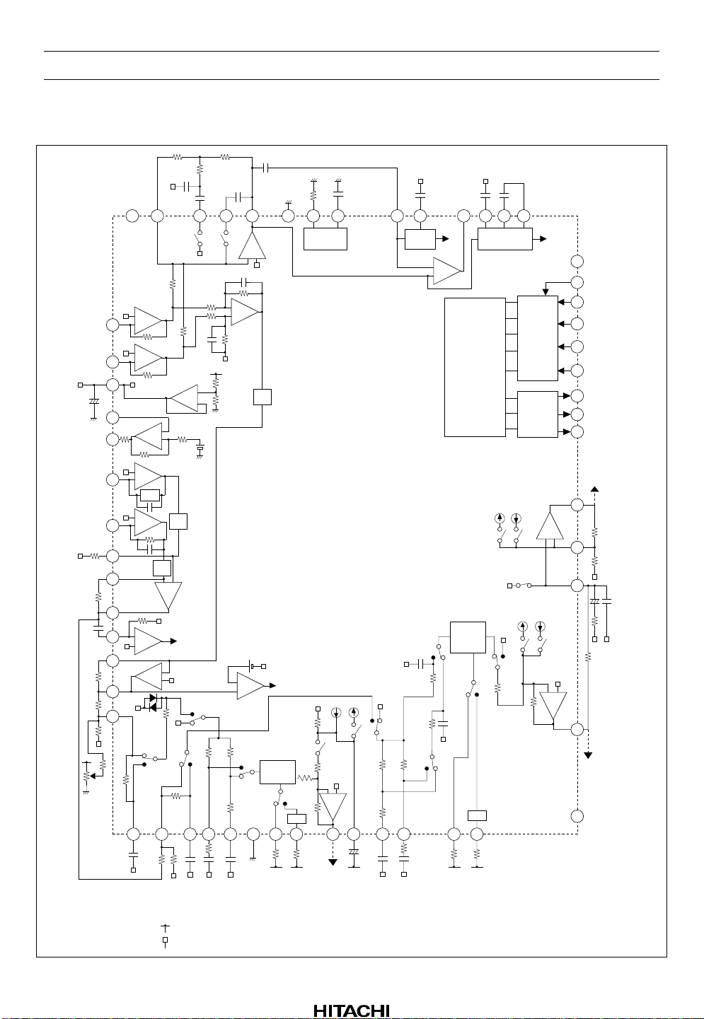
Block Diagram
V
CC
40
RFS
RS2
RF1
+
–
43
RF2
+
–
44
45
+
APC
46
47
48
TR2
49
+
–
+
–
BAL
TR1
+
–
VR
RS1
–+
–
+
FE
+
–
VR
50
51
VR
–+
TE
52
+
53
–
FA
TZC
–
+
FS4
FZC
–
+
54
55
56
DS1
FLS
Phase
compen.
×2.7
FPS
Focus
bias
adj.
DS2
1 2 5 6
3 4 7 8 9
• The states of the IC’s internal switches at XRST = “L” are shown at block diagram.
• The black dot symbol of transfer switch shows on state.
• The symbols “ ” mean connecting to V
• The symbols “ ” mean connecting to pin 45.
CC
FS2
.
Bias
35363738394142
FS1
FSA
–+
FAC
DRIV.
TM1
11 1210 13 14
+
Mirror
THS
–
+
FOK
TLS
Logic
Phase
compen.
×2.7
3134 32 30 2933
Defect
TM5 TM6
TM7
TPS
Input
I/F
Output
I/F
TM2
TM3 TM4
–+
TSA
–+
SSA
28
27
26
25
24
23
22
21
20
19
18
17
16
15
TAC
DRIV.
LDS
CLK
DATA
XLT
DC
XRST
SENS
COUT
DEFECT
or DRT
SLM
DRIV.
+
V
CC
Rev.1, Oct. 1995, page 2 of 35
HA12188AF
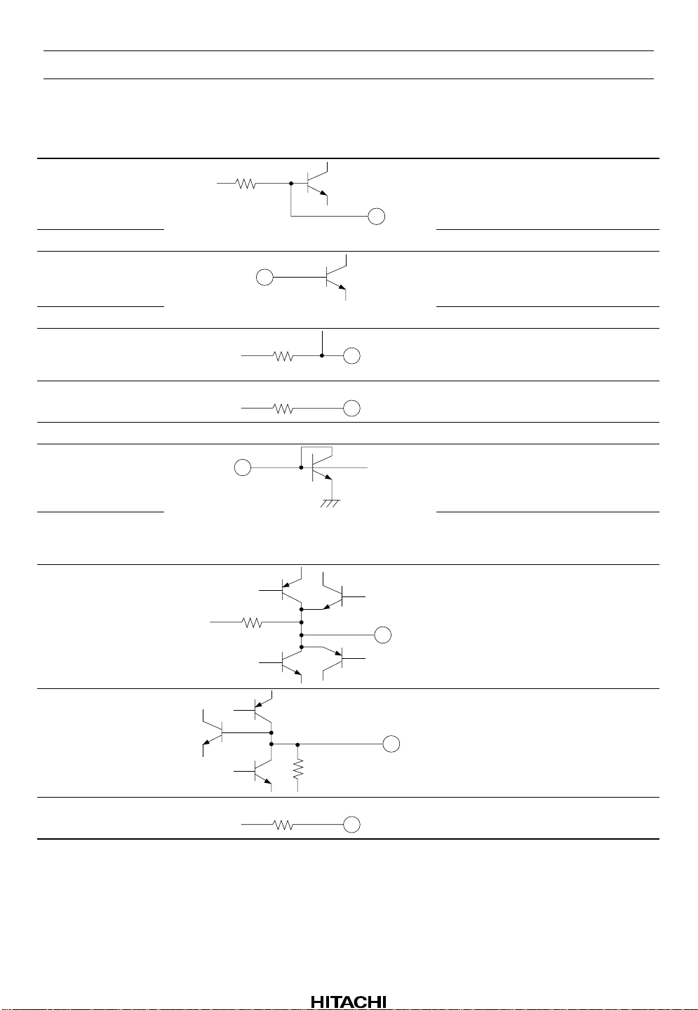
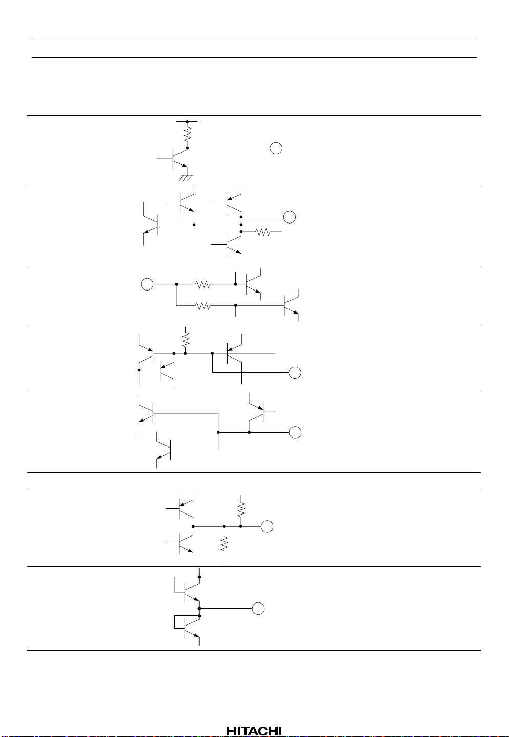
Pin Descriptions and Equivalent Circuits
Pin No. Symbol Equivalent Circuit Function
1FH
3 TH Tracking error hold signal output
2TSI Tracking servo input
56 FSI Focus servo input
4FLS
5 FLS
6 SGND — Servo ground
7 FPS Resistor connection for programming
470 k
90 k
30 k
Focus error hold signal output
Focus-servo low-frequency filter
resistor & capacitor connection
(FLS on)
Focus-servo low-frequency filter
capacitor connection (FLS off)
focus-servo phase compensation
(FPS off)
8 FPS Resistor connection for programming
focus-servo phase compensation
(FPS on)
9FSA
10 FS1
11 TLS
20 k
20 k
33 k
Focus servo output
FS1 voltage output
Tracking servo low-frequency filter
capacitor connection (TLS off)
Rev.1, Oct. 1995, page 3 of 35
HA12188AF
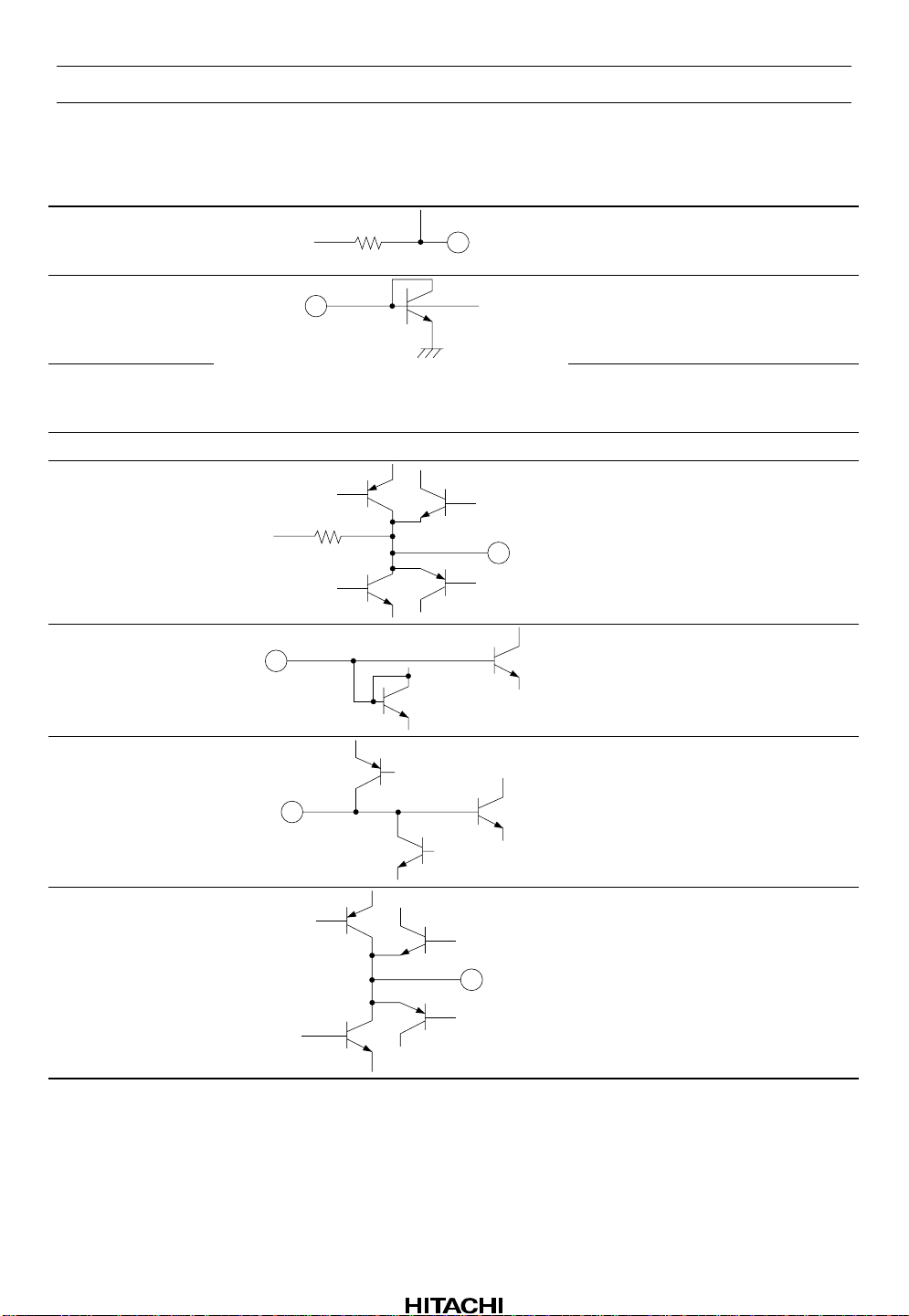
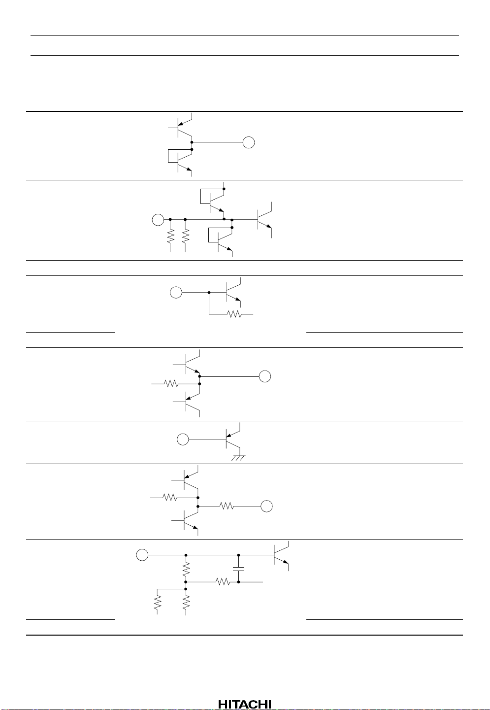
Pin Descriptions and Equivalent Circuits (cont)
Pin No. Symbol Equivalent Circuit Function
12 TLS
13 TPS Resistor connection for programming
14 TPS Resistor connection for programming
15 SV
16 TSA
CC
— Servo power supply
100 k
22 k
Tracking servo low-frequency filter
resistor & capacitor connection
(TLS on)
tracking servo phase compensat ion
(TPS off)
tracking servo phase compensat ion
(TPS on)
Tracking servo output
17 TM2 Sled serv o input
18 SSM SSA amplifier inverting input
19 SSA Sled servo output
Rev.1, Oct. 1995, page 4 of 35
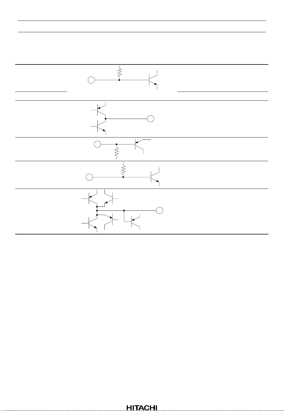
Pin Descriptions and Equivalent Circuits (cont)
Pin No. Symbol Equivalent Circuit Function
20 DRT
21 COUT COUT output
22 SENS SENS output
23 XRST Reset input
24 DC DC input
25 XLT XLT input
26 DATA Data input
27 CLK Clock input
28 LDS
10 k
50 k
V
CC
Defect signal output or inner/outer
direction signal output
Laser switch input
HA12188AF
50 k
29 DFIN
30 DFO Defect envelope signal output
31 DFH Defect hold signal output
43 k
Defect comparator input
Rev.1, Oct. 1995, page 5 of 35
HA12188AF
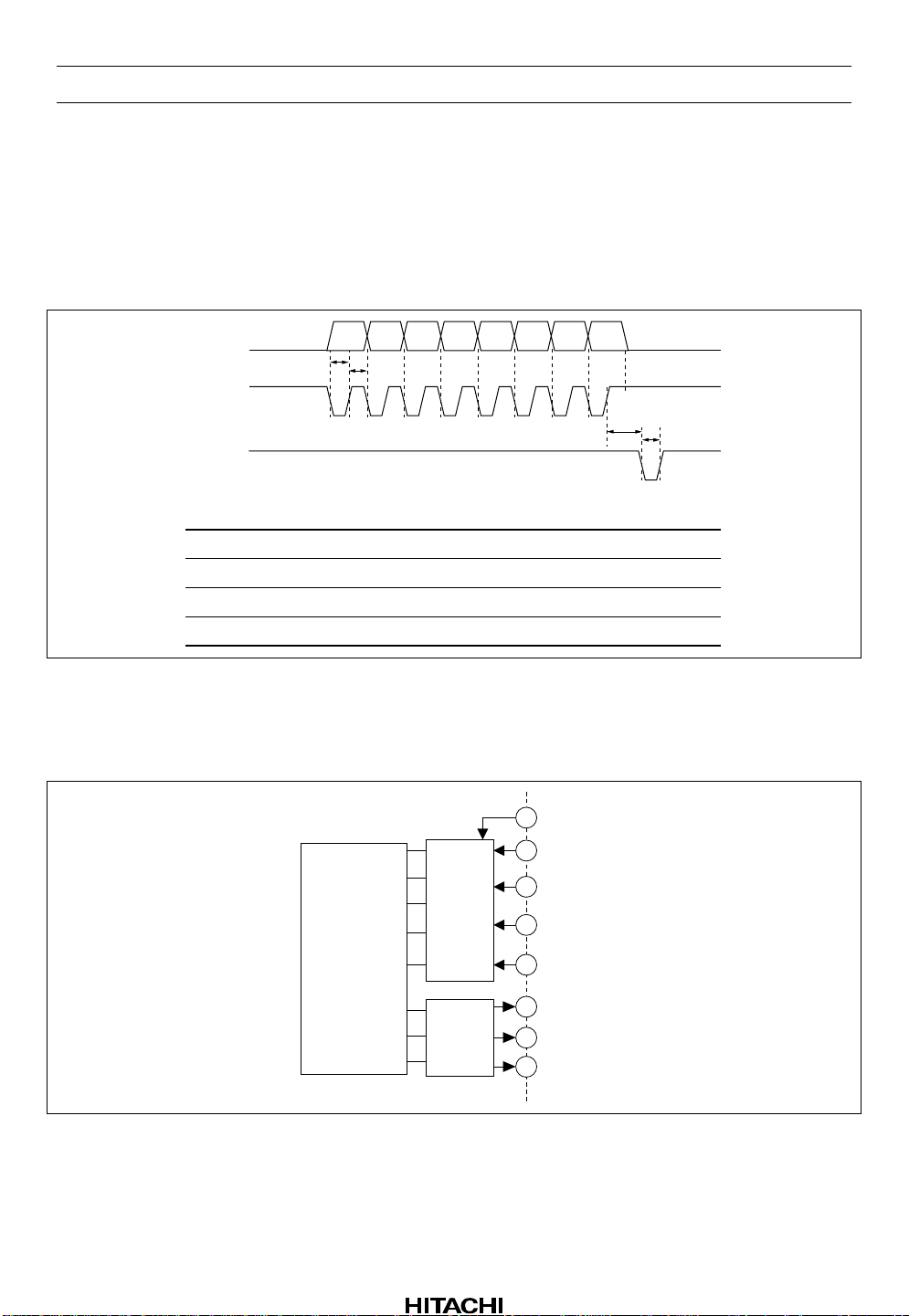
Pin Descriptions and Equivalent Circuits (cont)
Pin No. Symbol Equivalent Circuit Function
32 FOK
V
CC
20 k
FOK comparator output
33 MIRH
100 k
34 RFA
35 BYPS
36 ISET Resistor connection for programming
37 PGND — Pre-amplifier ground
38 RFO
40 k
18 k
20 k
18 k
Mirror hold signal output
RF signal AC input
Capacitor connection for ripple filter
reference current
RF signal output
40 k
39 RS1 RS1 switch
Rev.1, Oct. 1995, page 6 of 35
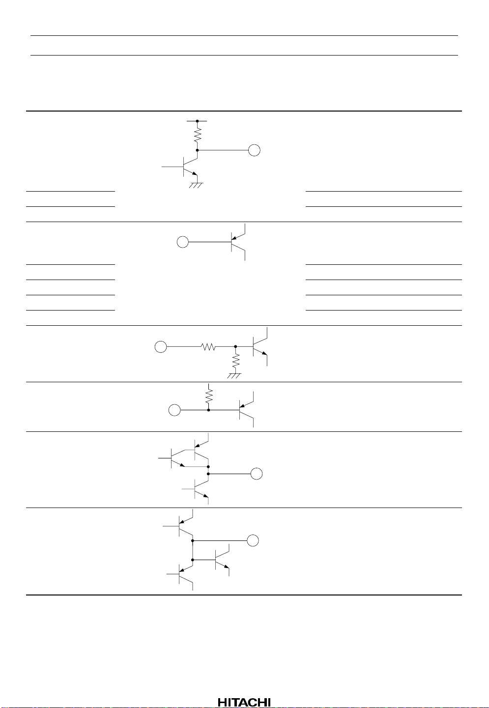
Pin Descriptions and Equivalent Circuits (cont)
Pin No. Symbol Equivalent Circuit Function
40 RS2
RS2 switch
HA12188AF
41 RFM
42 PV
43 RF1
5 k 5 k
CC
— Pre-amplifier power supply
10 k
RFS amplifier inverting input
RF1 amplifier input
44 RF2 RF2 amplifier input
45 V
C
20 k
Voltage reference output
46 MD APC amplifier input
47 LD
APC amplifier output
48 TR1
20 k
150 k
80 k
16 k
1 k
TR1 amplifier input
3.6 p
32 k
49 TR2 TR2 amplifier input
Rev.1, Oct. 1995, page 7 of 35
HA12188AF
Pin Descriptions and Equivalent Circuits (cont)
Pin No. Symbol Equivalent Circuit Function
50 TEP
51 TEM TE amplifier inverting input
52 TEO TE amplifier output
22.6 k
TE amplifier non-inverting input
53 TZC
75 k
54 FAM
55 FAO FA amplifier output
5.5 k
TZC comparator input
FA amplifier inverting input
Rev.1, Oct. 1995, page 8 of 35
HA12188AF
Operation
1. Microprocessor Control
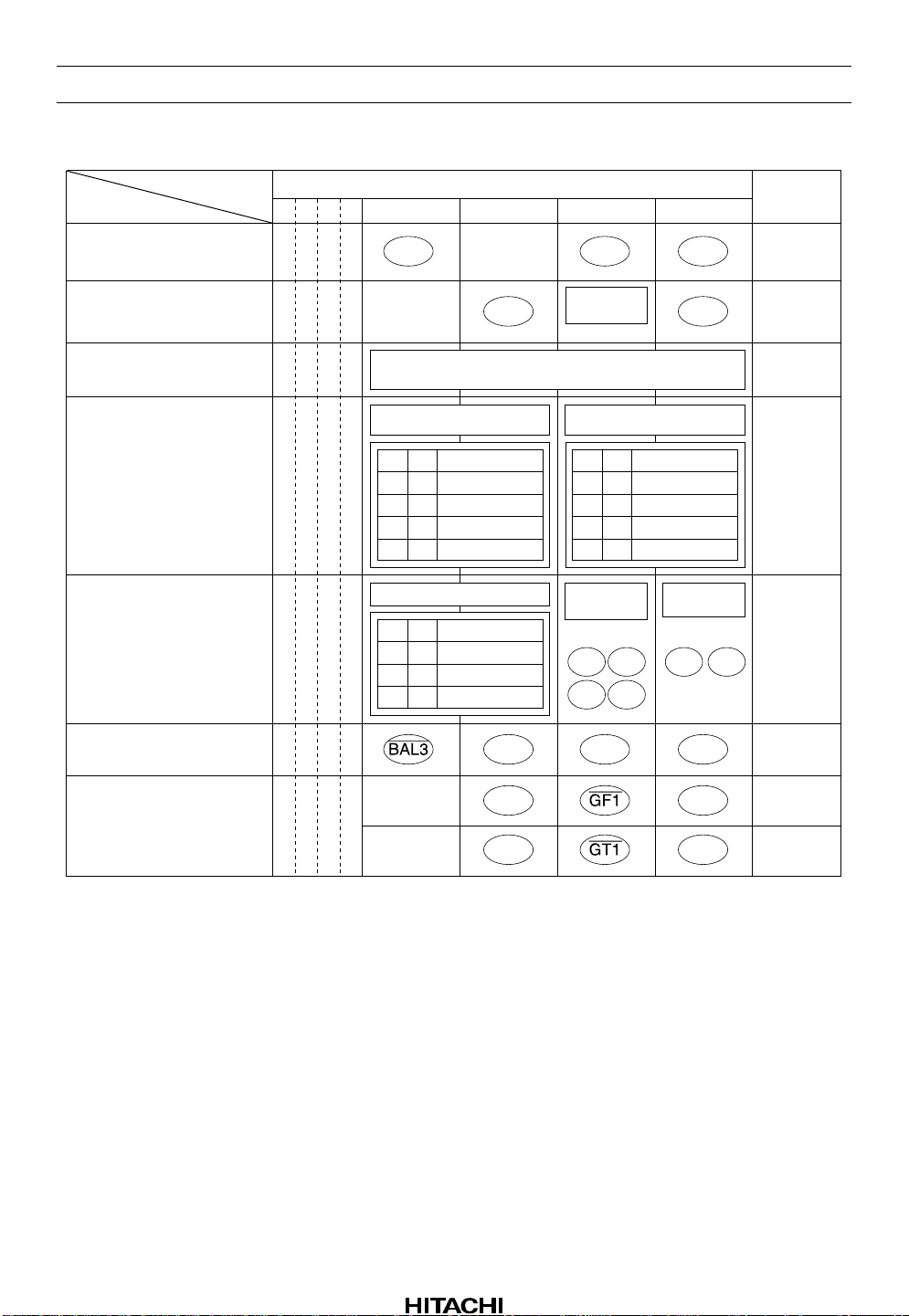
The IC’s internal switches can be operated by sending control data from a microprocessor. The signal
timing is shown in figure 1, and the control commands are listed in table 1.
DATA
CLK
XLT
Item
Clock frequency
Clock pulse width
Delay time
Latch pulse width
01234567
T1
T2
Symbol
f
CLK
T1, T2
T3
T4
Min
—
0.96
1
2
Typ
—
—
—
—
T3
Max
520
—
—
—
T4
Unit
kHz
µs
µs
µs
Figure 1 Timing Diagram for Microprocessor Control
Signals from the microprocessor are input at pins 23 to 27. A low input at the XRST pin resets the IC.
Normally this pin should be kept high. (See figure 2.)
27
CLK
26
DATA
25
Input
I/F
Logic
Output
I/F
XLT
24
DC
23
XRST
22
SENS
21
COUT
20
DEFECT
or DRT
Figure 2 Microprocessor Interface
Rev.1, Oct. 1995, page 9 of 35
HA12188AF
Table 1 Microprocessor Control Commands
D7D6D5D4 D3 D2 D1 D0
Focus mode
Tracking mode and FS1
DRT setting
0000
0001
FS4
*3
DRT
0: Defect
1: Direction
*1
DATA
DEFECT
OFF
*2
*4
TM7 THS H
FS2 FS1 FZC
FS1 current
*5
SENS
Access control mode
Pulse setting mode
Speed setting mode
EF balance adjustment
Tracking gain and focus
gain adjustment
Notes: 1.
The switch name surrounded by circle means that the switch turns on when the corresponding
bit is “1”. The switch name with bar surrounded by circle means that the switch turns on when
the corresponding bit is “0”.
“DEFECT OFF” means that switches DS1 and DS2 don’t turn on when the corresponding bit
2.
is “1”. Though the “DEFECT OFF” bit is set, the output at pin 20 is defect signal (in defect
signal output mode).
DRT (pin 20) outputs defect signal when the corresponding bit is “0”, and outputs direction
3.
signal when the corresponding bit is “1”.
TM7 can turn on only when COUT is high.
4.
The value of two current sources over switch FS1 are 18 µA(source) 36 µA(sink) when the
5.
corresponding bit is “1”, and are 9 µA(source) 18 µA(sink) when the corresponding bit is “0”.
The current values through switches TM3, TM4, TM5 and TM6 can be selected in four steps.
6.
The speed of Mirror circuit can be selected in three steps. Don’t use D3 = “1”, D2 = “0” mode.
7.
0010
0011
0100
0101
0110
D3
D3
0 ;
1 ; Tracking
D2
0
0
1
1
D2
0
0
1
Focus
gain
gain
0
1
0
1
0
1
1
Current value
Mirror
See table 2
*6 *6
32µA
16µA
24µA
8µA
*7
Mode
Normal
Double
Quadruple
BAL2 BAL1 BAL0 H
GF2 GF0 H
GT2 GT0
TM5, TM6 currentTM3, TM4 current
D1
D0
0
0
0
1
1
0
1
1
Focus
tracking
FLS FPS
TLS TPS
Current value
32µA
16µA
24µA
8µA
RF
RS1 RS2
TZC
H
H
H
Rev.1, Oct. 1995, page 10 of 35
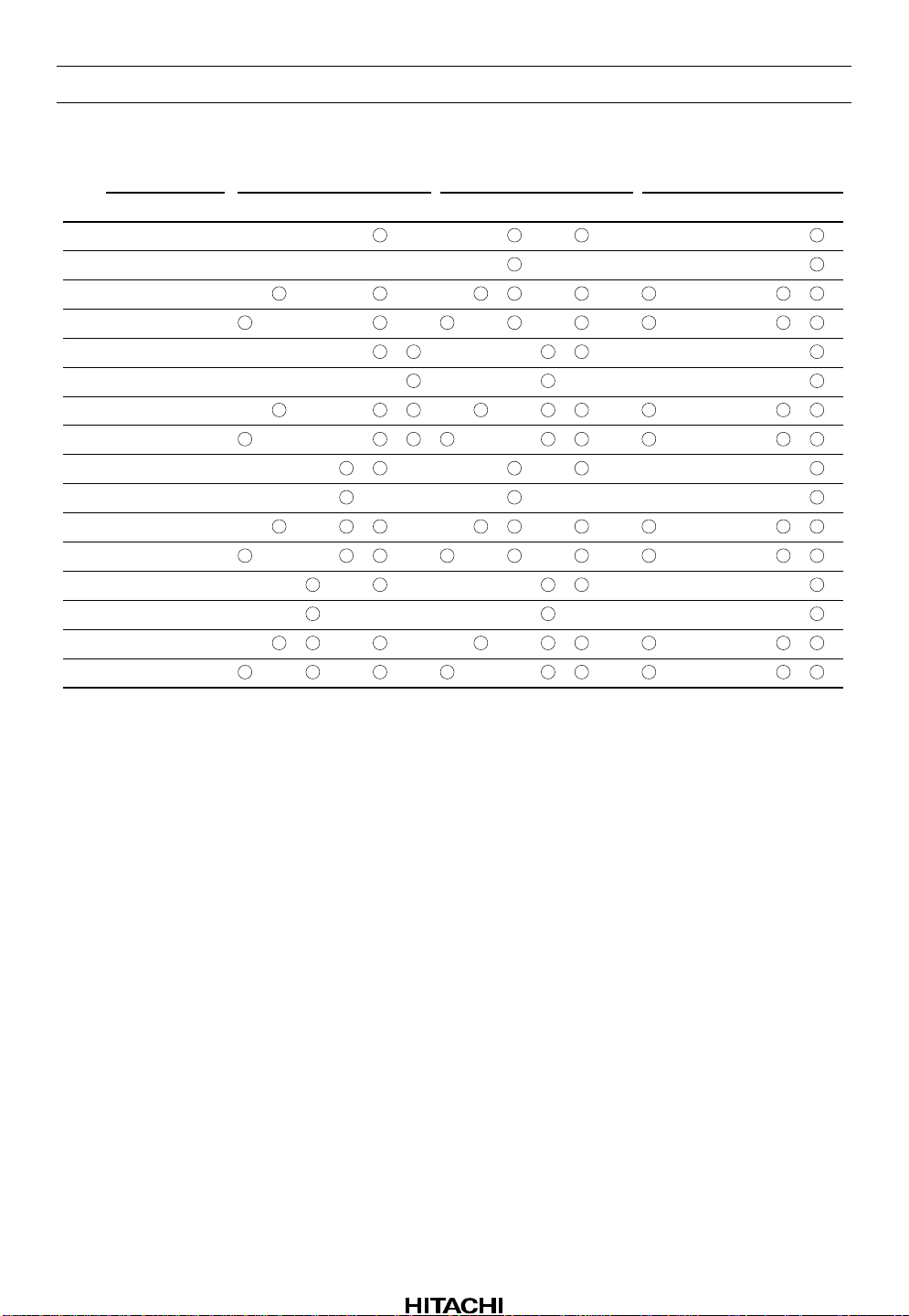
Table 2 Access Control Mode
HA12188AF
ST3
$20
$21
$22
$23
$24
$25
$26
$27
$28
$29
$2A
$2B
$2C
$2D
$2E
$2F
DATA ST1 ST2
D3
D2
D1
D0
0
0
0
0
0
0
0
1
0
0
1
0
0
0
1
1
0
1
0
0
0
1
0
1
0
1
1
0
0
1
1
1
1
0
0
0
1
0
0
1
1
0
1
0
1
0
1
1
1
1
0
0
1
1
0
1
1
1
1
0
1
1
1
1
TM5 TM4 TM3 TM2 TM1 TM6 TM5 TM4 TM3 TM2 TM1 TM6 TM5 TM4 TM3 TM2 TM1
TM6
A circle means that the switch is ON.
Note: After the microprocessor sends serial data, TM1 to TM6 can be switched among the states listed
under ST1 to ST3 by input at the DC pin. First, if the microprocessor sends serial data when DC is
high, TM1 to TM6 are placed in the state listed under ST1. When DC is brought low, the states
change to the states listed under ST2. Then if DC is brought high again, the states change to the
states listed under ST3.
Rev.1, Oct. 1995, page 11 of 35
 Loading...