


HA12181FP
AM Radio Noise Reduction System
ADE-207-171A (Z)
2nd. Edition
June 1997
Functions
• Buffer amp. for audio
• Linear approximate circuit for noise reduction
• IF Amp., detector, audio amp. and AGC circuit for noise detection
• Gate pulse generator
Features
• High noise cancelling capacity: 46 dB typ.
• Less gain loss: G
• Low total harmonic destortion and high signal-to noise ratio: THD = 0.06% typ., S/N = 75 dB typ.
• Operation supply voltage range: 7.0 V to 10 V (8.2 V typ.)
• Less external parts count
= –0.5 dB typ.
V
HA12181FP
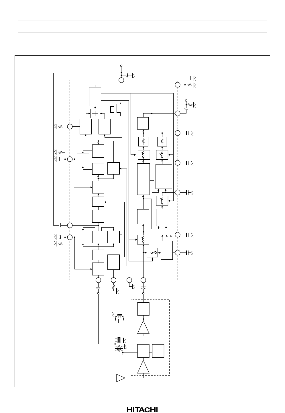
Block Diagram
R502
R505
47 k
C504
0.22µ
C503
0.01µ
C502
+
22 k
12
AF AGC
Det.
3.3µ
114 15
Pulse
OR
IF
AGC
Gen.
Gate pulse
Det.(1)
Noise
AF
AF
LPF
HPF1
Det.
Pulse
Det.(2)
AGC
AGC
Amp.
VCC(8.2 V)
13
(2)
(1)
HPF
Det.
Pulse
+
C506
100µ
Buffer
Amp.
Gate pulse (1)
Gate pulse (2)
SW4
Hight-pass Amp.
(waveform
Phase
Circuit
SW2
SW5
Stabilized
Current Circuit
compensation)
(waveform
SW3
Level Diff.
Det.
Circuit
C507
Gate Time
Constant
119
R503
180 k
AF Output
+
C508
C509
0.033µ
108652
Capacitor
for By-pass
compensation)
Capacitor
for Hold
Capacitor
for Pahse
2200 p
R504
4.7 k
1µ
Capacitor
for waveform
C510
0.033µ
C511
0.033µ
C512
0.068µ
C : F
Unit R : Ω
compensation
R500
100 k
IF AGC
Rev.2, Jun. 1997, page 2 of 21
LPF
IF
Amp.
16
C501
IF Input
Volt.
Stabi.
4
1000 p
2nd IFT
1st IFT
ANT
R506
12 k
7
SW1
3
+
C513
AF Input
Det.
IF
MIX
RF
1µ
Stabilized
Voltage
AM-IC
OSC
Circuit
C500
0.033µ
HA12181FP
Table of Pin Description and External Parts
Influence of External
External parts
DC
No.
of
pin Name Function
voltage
(V) (No
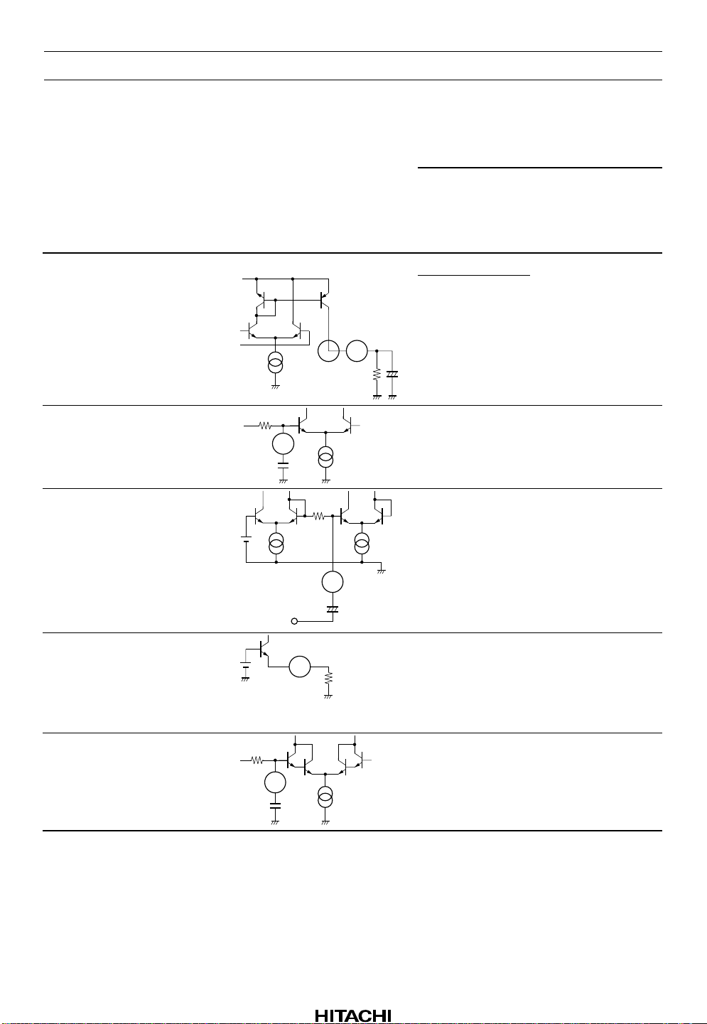
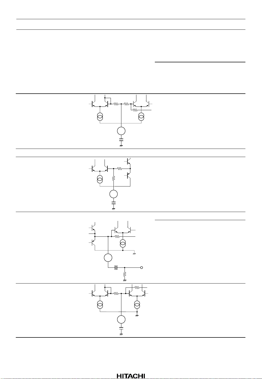
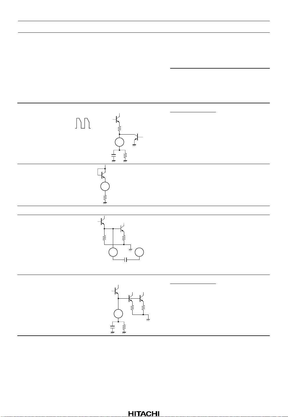
input) Equivalent circuit No.
recommended
value
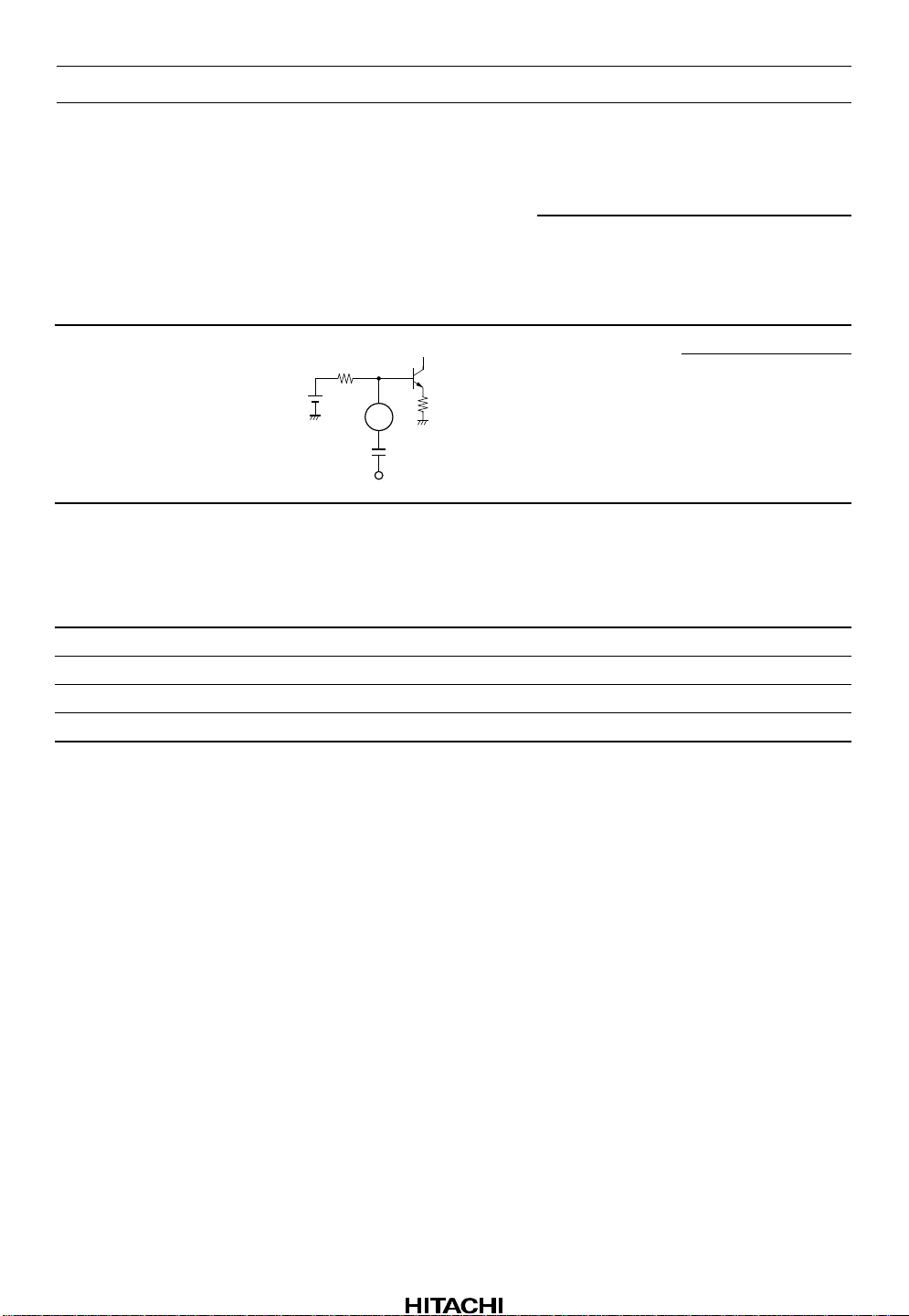
1 IF AGC Time 2.7 R500 100 K Longer Longer
constant
C502 3.3 µ time to
for IF
AGC.
C502
3.3µ
1
R500
100k
+
parts
Larger
than
recommended
value
stabilize
AGC.
Smaller
than
recommended
value
distortion
of recover.
2 Bias1 Bypass
for
voltage
Stabi.
3AF
input
Input of
AF.
4 Bias2 Decide
the
current of
filter
network.
5 Phase Phase
circuit
3.2
3.3
1.3
3.3
C500
0.033µ
AF IN
2
5
4
C512
0.068µ
20k
3
+
C513
C500 0.033 µ — Increased
noise.
C513 1 µ — —
R506 12 K Cut off
frequency
of L·P·F
and H·P·F
shifted
lower.
Cut off
frequency
of L·P·F
and H·P·F
shifted
higher.
C512 0.068 µ Must be used on the
recommended value.
Rev.2, Jun. 1997, page 3 of 21
HA12181FP
Table of Pin Description and External Parts (cont)
Influence of External
External parts
DC
No.
of
pin Name Function
6 Hold Hold of
voltage
(V) (No
input) Equivalent circuit No.
3.3
C511 0.033 µ Must be used on the
recommended
value
level
difference.
6
C511
0.033µ
7GNDGND — — — — —
8 High-
Pass.
HighPass
3.3
C510 0.033 µ Must be used on the
AMP.
(Waveform
Compensation)
8
C510
0.033µ
parts
Larger
than
recommended
value
Smaller
than
recommended
value
recommended value.
recommended value.
9 AF out Output of 3.3 C508 1 µ Output DC cut
AF
9
R504 4.7 K Output load
+
10 Wave
form
Waveform
C508
3.3
1µ
R504
4.7k
C509 0.033 µ Must be used on the
recommended value.
Compensation
10
C509
0.033µ
Rev.2, Jun. 1997, page 4 of 21
HA12181FP
Table of Pin Description and External Parts (cont)
Influence of External
External parts
DC
No.
of
pin Name Function
voltage
(V) (No
input) Equivalent circuit No.
recommended
value
11 Gate Gate R503 180 K Gate Gate
pulse
4.5V
C507 2200 P pulse
generation
0
11
parts
Larger
than
recommended
value
width
become
wider.
Smaller
than
recommended
value
pulse
width
become
narrow.
R503
180k
R502 22 K Higher
noise
detection
sensitivity.
Lower
noise
detection
sensitivity.
C503 0.01 µ — —
12 Vth Determi-
nation of
noise
detection
sensitivit
y
13 V
V
CC
CC
14 IF Det. IF AGC
C507
2200p
1.1
12
R502
22k
8.2 — — — — —
3.3
detector
14 13
C503
0.01µ
15 AF Time 0 R505 47 K Longer Miss-
AGC constant
for AF
AGC
C504 0.22 µ time to
stabilize
AGC.
operaton
in noise
detector.
15
C504
0.22µ
R505
47k
Rev.2, Jun. 1997, page 5 of 21
HA12181FP
Table of Pin Description and External Parts (cont)
Influence of External
External parts
DC
No.
of
pin Name Function
voltage
(V) (No
input) Equivalent circuit No.
recommended
value
16 IF in IF input 1.3 IF Input Coupling
30k
16
C501
1000p
IF IN
Absolute Maximum Ratings (Ta = 25°C)
Item Symbol Rating Unit
Supply voltage V
CC
Power dissipation Pd 400*
Operating temperature Topr –40 to +85 °C
Storage temperature Tstg –55 to +125 °C
Note: 1. Value at Ta = 85°C
16 V
1
parts
Larger
than
recommended
value
Smaller
than
recommended
value
— Instability
mW
Rev.2, Jun. 1997, page 6 of 21
HA12181FP
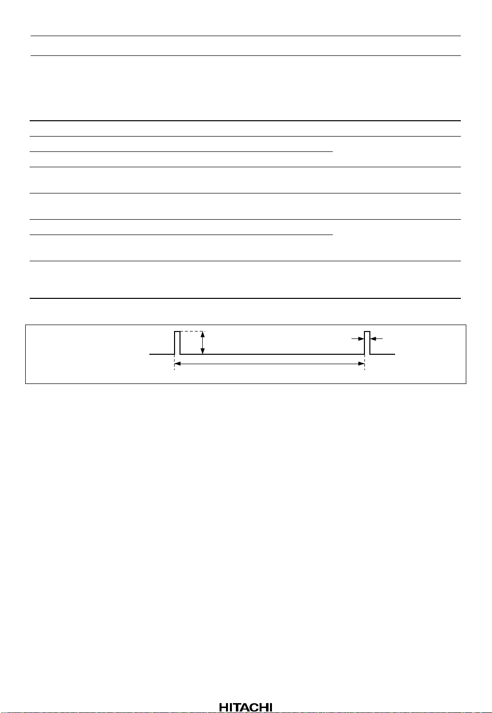
Electrical Characteristics (Tentative) (VCC = 8.2 V, Ta = 25°C, Pin 3 input: Vin = 100
mVrms, f = 1 KHz, Pin 16 input: Vin = 74 dBµ, fc = 450 KHz, fm = 1 KHz, m = 30%)
Item Symbol Min Typ Max Unit Test conditions
Supply current I
Output voltage Vout 70 95 120 mVrms Pin 3 input only
Total harmonic distortion THD1 — 0.06 0.3 %
Signal-to-noise ratio S/N (1) 60 75 — dB Pin 3 input Vin = 100 mVrms
Strong input total harmonic
distortion
Recovered output voltage VO (AF) 50 78 120 mVrms Pin 16 input only
Recovered output signal-to-
noise-ratio
Noise suppression ratio NSR 35 46 — dB Input the waveform below.
CC
THD2 — 1.0 2.5 % Pin 3 input Vin = 500 mVrms
S/N (2)3545—dB
— 11.0 — mA No input signal, IC only
(Reference), Rg = 10 KΩ
Pin 3 input Vin = 100 mVrms
(Reference) no input sine wave
100mV
Pin 16 Input
2ms
10µs
Figure 1 Input Waveform at Measurement of Noise Suppression Ratio
Rev.2, Jun. 1997, page 7 of 21
HA12181FP
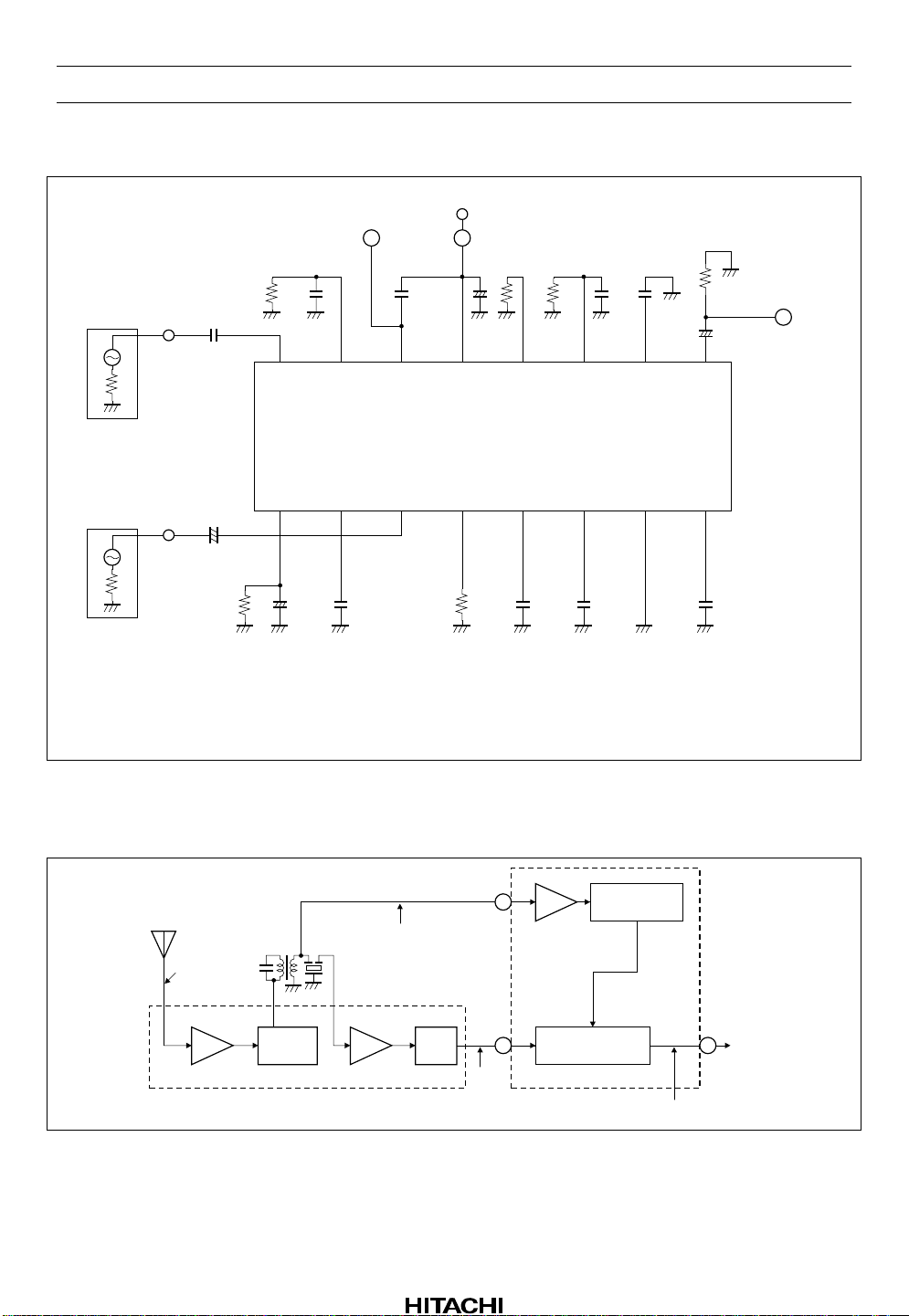
Test Circuit
IF-IN
PULSE-IN
50
AM-SG
AF-IN
50
AF-SG
C501
1000p
+
C513
1µ
R500
100k
VCC (8.2V)
Det.Out
C504
R505
0.22µ
47k
16
12345678
+
C502
3.3µ
B
15 14 13 12 11 10 9
C500
0.033µ
C503
0.01µ
R506
12k
+
A
+
C506
100µ
R502
15k
C512
0.068µ
R503
180k
C511
0.033µ
C507
2200p
C509
0.033µ
0.033µ
C510
R504
4.7k
C508
+
1µ
C
OUT
Note: 1. Resistors tolerance are within ±5%.
2. Capacitors tolerance (C509 to C512) are within ±5%, other capacitor are within ±10%.
Operation Principle
Noise
Detector
9
D
ANT.
16
IF
1st IFT
B
A
RF
CONV.
IF
DET
3
Processing
Waveform Circuit
C
AM-IC
HA12181FP
Figure 2 System Block Diagram of AM Radio
Unit R : Ω
C : F
Out
Rev.2, Jun. 1997, page 8 of 21
HA12181FP
A system block diagram of AM Radio using the HA12181FP is shown in Figure 2 and waveforms at each
point in the system are illustrated in Figur e 3. Fo r AM wave with im pulse noise from ANT, the pulse
spreads its width each time when the AM wave passes through a selection filter.
The pulse width becomes the order of several hundred microseconds at detector output (Point C).
A radio without a noise canceller produces large noise to the audience. This IC perfectly detects every
noise by using the signals from 1st IFT (Poin t B) in front of the narrow band filter.
The wave process circuit approximates the voltage linearly at the pulse to reduce the noise in the output.
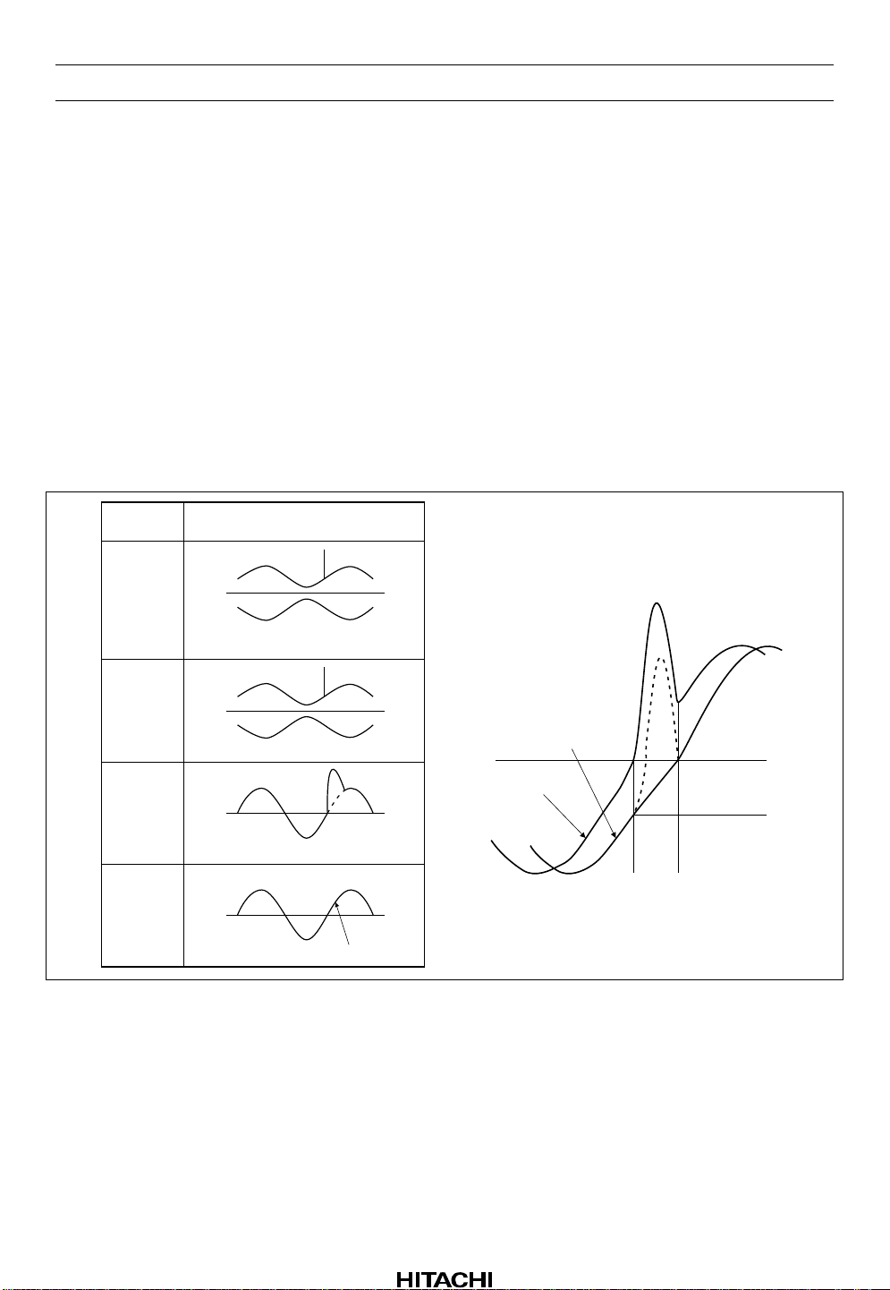
The principle for wave processing follows. Further investigation make it clear that the pulse width of
impulse noise is constant (several handred microseconds) and independent of the waveform or waveheight.
Therefore the former and later voltage (VA, VB) of the pulse can be found at the same time (T1) by means
of the wave and the delayed one for this time, as shown in the right figure.
Each Point
in the Figure
A
B
C
D
Waveform including Noise
Narrower Pulse Width
and Higher Wave Height
Wider Pulse
Width and Lower Wave Height
Noiseless
Figure 3 Waveforms at Each Point in the System
Point D
Point C
V
B
V
A
T
T
1
2
In an actual circuit, the differential voltage between input and output of phase shif t circuit is changed to the
capacitor C511 at pin 6.
At the time of T1, when the switch turns to the noise processing mode (the switch positions in Figure 4 are
inverted), the voltage difference (VA – VB) is held in C511.
C509 at pin 10 is changed by the differential voltage between the held voltage and the output voltage at pin
9 (VA): VA – (VA – VB) = VB.
Rev.2, Jun. 1997, page 9 of 21
HA12181FP
As the initial voltage of C509 is equal to th e ou tput v oltage (VA) before the switch change, the voltage
between terminals of C509 is changed from VA to VB.
The waveform which change up to C509 becomes the output, because the voltage of C509 appears at pin 9
through the buffer.
The changed up waveform of C509 is almost linearly approximated because of the constant current change
by the feedback from the output at pin 9.
At the time of T2 when the awitches change to the normal mode (the switch position in Figure 4), the
output recovers smoothly as the voltage of C509 is VB.
However the unmatch of the wave delay time due to the pulse width or the phase circuit and the offset of
circuit make a slight step difference on the waverform at the moment of switch change.
LPF, consisting of R1 and C509 make it smooth.
The frequency characteristics, which is detriorated by LPF in the normalmode, is compensated so that it
might become flat. C509 and C510 should have the same capacity, and the tolerance must be within ±5%.
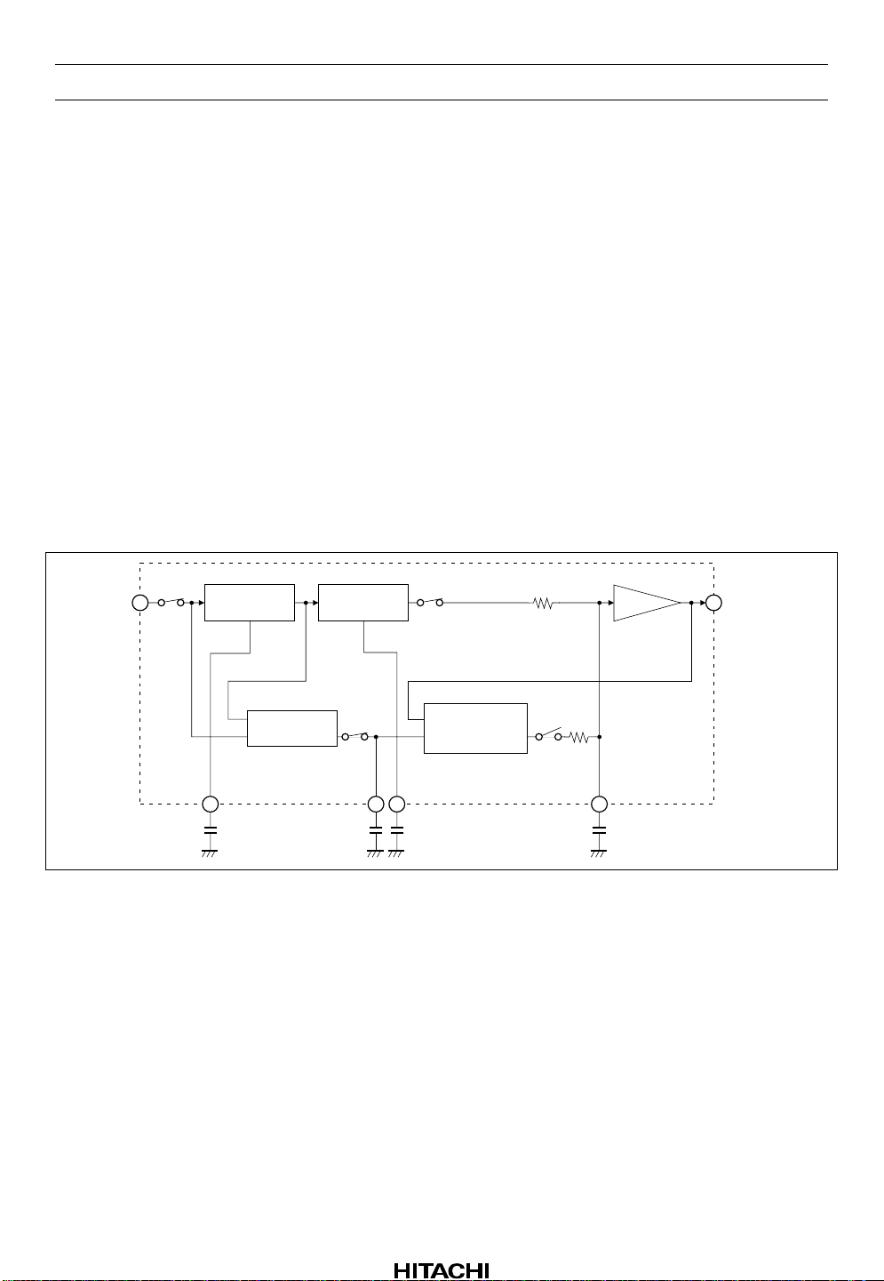
3
Phase
Circuit
5
C512
+
Subtraction
–
Circuit
HPFAmp.
6 8
C511
+
Constant Current
Circuit(Subtraction
–
Circuit)
C510
R1
R2
10
Buffer
C509
9
Out
Figure 4 Waveform Processing Circuit
Rev.2, Jun. 1997, page 10 of 21
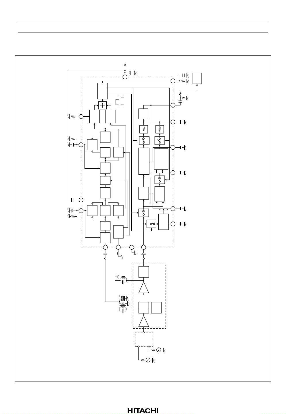
Evaluation Circuit for Noise Reduction Effect
HA12181FP
R502
R505
47 k
C504
C503
0.01µ
+
R500
100 k
22 k
12
AF AGC
0.22µ
Det.
C502
3.3µ
114 15
IF AGC
Pulse
OR
IF
Gate pulse
Det.(1)
AGC
IF Input
Gen.
Pulse
AGC
Noise
AF
AGC
AF
Amp.
LPF
HPF1
Det.
LPF
IF
Amp.
16
Det.(2)
C501
1000 p
VCC(8.2 V)
13
(2)
(1)
HPF
Det.
Pulse
Volt.
Stabi.
4
R506
+
C506
100µ
Buffer
Amp.
Gate pulse (1)
Gate pulse (2)
SW4
Hight-pass Amp.
(waveform
Phase
Circuit
SW2
3
7
+
12 k
AF Input
SW5
Stabilized
Current Circuit
(waveform
compensation)
SW3
Level Diff.
Det.
Circuit
SW1
Stabilized
Voltage
C513
1µ
C507
Gate Time
Constant
119
R503
180 k
AF Output
+
0.033µ
C509
108652
Capacitor
for By-pass
compensation)
Capacitor
for Hold
Capacitor
for Pahse
Circuit
C500
0.033µ
2200 p
R504
4.7 k
C508
1µ
Capacitor
for waveform
C510
0.033µ
C511
0.033µ
C512
0.068µ
Noise
Meter
Unit R : Ω
compensation
C : F
2nd IFT
1st IFT
Two signals
dummy ANT.
Det.
IF
MIX
RF
50
Pulse SG.
AM-IC
OSC
50
AM SG.
Rev.2, Jun. 1997, page 11 of 21

HA12181FP
Example of Noise Reduction Effect
20
10
0
–10
–20
Output (dB)
–30
–40
Pulse : No input
–50
–60
0 10 20 30 40 50 60 70 80 90 100 110
AM SG : fc=999kHz, m=30%, fm=1kHz
Pulse : No input
Two Signals dummy ANT.
50Ω
NRoff
Pulse SG.
AM SG.
50Ω
NRon
AM SG Output (EMF) (dBµ)
VCC=8.2V
Vout
16Ω
16Ω
30Ω
16Ω
Noise
15p
To
ANT
65p
Pulse SG Output (EMF)
10µs
100mV
2µs
Figure.2
P-P
AM SG : fc=999kHz,
no mod.
Pulse SG :
Refer to Figure.2
120
20
VCC=8.2V
Pulse : No input
Two Signals dummy ANT.
50Ω
16Ω
16Ω
50Ω
16Ω
Noise
Vout
15p
To
ANT
30Ω
65p
AM SG : fc=999kHz,
no mod.
Pulse SG :
Refer to Figure.2
10
0
–10
–20
Output (dB)
–30
–40
NRon
AM SG : fc=999kHz, m=30%, fm=1kHz
Pulse SG.
NRoff
AM SG.
–50
–60
0 10 20 30 40 50 60 70 80 90 100 110
AM SG Output (EMF) (dBµ)
Pulse SG Output (EMF)
10µs
100mV
10µs
Figure.3
P-P
120
Rev.2, Jun. 1997, page 12 of 21
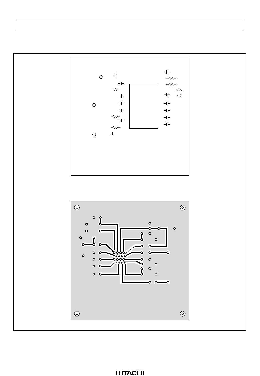
PC Board Layout Pattern
HA12181FP
IF in
AF in
V
CC
FN-8648
C502
C505
R501
R506
R500
+
+
C504
C503
C501
C513
C506
+
(Top view)
C507
R503
R502
R504
C508
+
C509
Vout
16
C510
C511
C512
HA12181FP
(Bottom view)
HA12181FP
Rev.2, Jun. 1997, page 13 of 21

HA12181FP
Main Characteristics
10
Vout (dB)
0
Vin max (Vrms)
-2
2.0
-4
1.5
-6
1.0
-8
0.5
-10
Vout : Vin = 100 mVrms const
Vout
(0 dB = 96 mVrms)
Vin Max
(THD ≥ 1.0%)
-12
0
40
0.5
0.4
0.3
THD (%)
0.2
0.1
100
0
40
100
400 1 k 2 k
200
200
f (Hz)
Vin = 100 mVrms
400 1 k 2 k
f (Hz)
10 k4 k 20 k 50 k
10 k4 k
Rev.2, Jun. 1997, page 14 of 21

10
Vo (AF) : 0 dB = 76 mVrms
0
-10
-20
fc = 450 kHz, m = 30%, fm = 1kHz
-30
Vout (dB)
-40
Noise (no modulation)
-50
-60
-70
10 20 30 40 50 60 70 80 90 100 110
Vin (EMF) (dBµ)
HA12181FP
120
50
Pulse input at Gate ON
20
10
5
2
V pulse (mVp-p)
1
0.5
0.2
1 k
10µs
2ms
5 k 10 k
V pulse
100 k50 k
R (Ω)
Rev.2, Jun. 1997, page 15 of 21

HA12181FP
120
THD1 (%)
100
0.5
80
0.4
60
0.3
40
0.2
20
0.1
0
Vout (mVrms)
Vout
THD1
0
678910111213141516
120
THD2 (%)
1.0
100
0.8
0.6
0.4
0.2
0
V
(V)
CC
S/N1 (dB)
S : 100 mVrms = 0 dB
N : no-input
80
S/N1
60
40
20
THD2 (Vin = 500 mVrms, f = 1 kHz)
0
678910111213141516
V
(V)
CC
Rev.2, Jun. 1997, page 16 of 21

Vo (AF) (mVrms)
S/N2 (dB)
60
120
HA12181FP
50
40
30
20
10
60
50
40
100
80
60
40
20
0
0
678910111213141516
60
50
40
S/N2
Vo (AF)
V
(V)
CC
NSR (pulse input)
Vin = 74 dBµ
fc = 450 kHz
fm = 1 kHZ
m = 30%
30
20
10
30
20
ICC (no-input)
10
0
0
678910111213141516
V
(V)
CC
Rev.2, Jun. 1997, page 17 of 21

HA12181FP
V pulse (mVp-p)
1.0
0.8
0.6
0.4
0.2
0
678910111213141516
V pulse (Pulse input level at Gate on)
V
(V)
CC
Vout (AF) (mVrms)
THD1 (%)
0.5
100
0.4
80
0.3
60
0.2
40
0.1
20
0
0
-40 -20 0 20 40 60 80 100
Rev.2, Jun. 1997, page 18 of 21
Vout
VCC = 8.2 V
Vin = 100 mVrms, f = 1 kHz
THD1
Ta ( C)

NSR (dB)
60
50
(mA)
CC
I
60
50
HA12181FP
VCC = 8.2 V
40
30
20
10
40
30
20
10
0
0
-40 -20 0 20 40 60 80 100
NSR (pulse input)
ICC (no-input)
Ta ( C)
Rev.2, Jun. 1997, page 19 of 21

HA12181FP
Package Dimensions
16
Unit: mm
10.06
10.5 Max
9
5.5
1
0.80 Max
1.27
0.42 ± 0.08
0.40 ± 0.06
8
0.10 ± 0.10
0.15
0.12
2.20 Max
M
7.80
0.22 ± 0.05
0.20 ± 0.04
0.70 ± 0.20
Hitachi Code
JEDEC Code
EIAJ Code
Weight
+ 0.20
– 0.30
1.15
0 – 8˚
FP-16DA
—
SC-530-16C
0.24 g
Rev.2, Jun. 1997, page 20 of 21

HA12181FP
Disclaimer
1. Hitachi neither warrants nor grants licenses of any rights of Hitachi’s or any third party’s patent,
copyright, trademark, or other intellectual property rights for information contained in this document.
Hitachi bears no responsibility for problems that may arise with third party’s rights, in cluding
intellectual property rights, in connection with u se of the information contained in this document.
2. Products and product specifications may be subject to change without notice. Confirm that you have
received the latest product standards or specifications before final design, purchase or use.
3. Hitachi makes every attempt to ensure that its products are of high quality and reliability. However,
contact Hitachi’s sales office before using the product in an application that demands especially high
quality and reliability or where its failure or malfunction may directly threaten human life or cause risk
of bodily injury, such as aerospace, aeronautics, nuclear power, combustion control, transportation,
traffic, safety equipment or medical equipment for life support.
4. Design your application so that the product is used within the ranges guaranteed by Hitachi particularly
for maximum rating, operating supply voltage range, heat radiation characteristics, installation
conditions and other characteristics. Hitachi bears no responsibility for failure or damage when used
beyond the guaranteed ranges. Even within the guaranteed ranges, consider normally foreseeable
failure rates or failure modes in semiconductor devices and employ systemic measures such as failsafes, so that the equipment incorporating Hitachi product does not cause bodily injury, fire or other
consequential damage due to operation of the Hitachi product.
5. This product is not designed to be radiation resistant.
6. No one is permitted to reproduce or duplicate, in any form, the whole or part of this document without
written approval from Hitachi.
7. Contact Hitachi’s sales office for any questions regarding this document or Hitachi semiconductor
products.
Sales Offices
Hitachi, Ltd.
Semiconductor & Integrated Circuits.
Nippon Bldg., 2-6-2, Ohte-machi, Chiyoda-ku, Tokyo 100-0004, Japan
Tel: Tokyo (03) 3270-2111 Fax: (03) 3270-5109
URL NorthAmerica : http://semiconductor.hitachi.com/
For further information write to:
Hitachi Semiconductor
(America) Inc.
179 East Tasman Drive,
San Jose,CA 95134
Tel: <1> (408) 433-1990
Fax: <1>(408) 433-0223
Europe : http://www.hitachi-eu.com/hel/ecg
Asia : http://sicapac.hitachi-asia.com
Japan : http://www.hitachi.co.jp/Sicd/indx.htm
Hitachi Europe GmbH
Electronic Components Group
Dornacher Straße 3
D-85622 Feldkirchen, Munich
Germany
Tel: <49> (89) 9 9180-0
Fax: <49> (89) 9 29 30 00
Hitachi Europe Ltd.
Electronic Components Group.
Whitebrook Park
Lower Cookham Road
Maidenhead
Berkshire SL6 8YA, United Kingdom
Tel: <44> (1628) 585000
Fax: <44> (1628) 585160
Hitachi Asia Ltd.
Hitachi Tower
16 Collyer Quay #20-00,
Singapore 049318
Tel : <65>-538-6533/538-8577
Fax : <65>-538-6933/538-3877
URL : http://www.hitachi.com.sg
Hitachi Asia Ltd.
(Taipei Branch Office)
4/F, No. 167, Tun Hwa North Road,
Hung-Kuo Building,
Taipei (105), Taiwan
Tel : <886>-(2)-2718-3666
Fax : <886>-(2)-2718-8180
Telex : 23222 HAS-TP
URL : http://www.hitachi.com.tw
Hitachi Asia (Hong Kong) Ltd.
Group III (Electronic Components)
7/F., North Tower,
World Finance Centre,
Harbour City, Canton Road
Tsim Sha Tsui, Kowloon,
Hong Kong
Tel : <852>-(2)-735-9218
Fax : <852>-(2)-730-0281
URL : http://www.hitachi.com.hk
Copyright Hitachi, Ltd., 2000. All rights reserved. Printed in Japan.
Colophon 2.0
Rev.2, Jun. 1997, page 21 of 21
 Loading...