


General Semiconductor SM15T33A, SM15T36A, SM15T7V5A, SM15T15A, SM15T18A Datasheet
...
SM15T SERIES
TRANSZORB™ SURFACE MOUNT TRANSIENT VOLTAGE SUPPRESSOR
Breakdown Voltage - 6.8 to 220 Volts Peak Pulse Power - 1500 Watts
FEATURES
♦ For surface mounted applications in order to
optimize board space
♦ Low profile package
♦ Built-in strain relief
♦ Glass passivated junction
♦ Low inductance
♦ Excellent clamping capability
♦ Repetition Rate (duty cycle): 0.05%
♦ Fast reponse time: typically less than 1ps from 0 volts to
V
BR
min.
♦ Typical I
D
less than 1µA above 10V
♦ High temperature soldering: 250°C/10 seconds
at terminals
♦ Plastic package has Underwriters Laboratory
Flammability Classification 94V-0
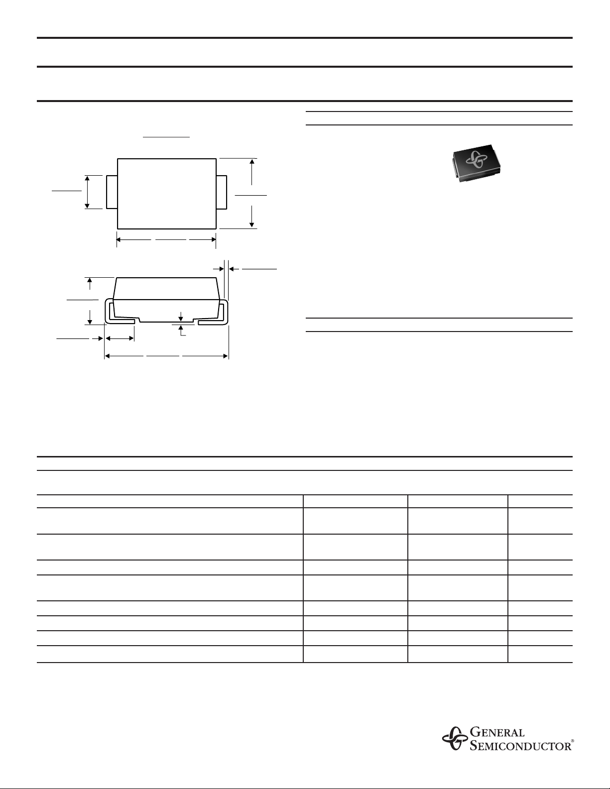
MECHANICAL DATA
Case: JEDEC DO-214AB (SMC) molded plastic over
passivated junction
Terminals: Solder plated solderable per MIL-STD-750,
Method 2026
Polarity: For uni-directional types: Color band
denotes positive end (cathode)
Standard Packaging: 12mm tape (EIA STD RS-481)
Weight: 0.003 ounces, 0.093 gram
MAXIMUM RATINGS AND ELECTRICAL CHARACTERISTICS
Ratings at 25°C ambient temperature unless otherwise specified
SYMBOLS VALUE UNIT
Peak Pulse Power Dissipation on 10/1000µs
waveform
(NOTES 1, 2, Fig. 1)
P
PPM
Minimum 1500 Watts
Peak Pulse Current on 10/1000µs
waveform
(NOTE 1, Fig. 3)
I
PPM
See Table 1 Amps
Power Dissipation on Infinite Heatsink, TA=50°CP
M(AV)
6.5 Watts
Peak Forward Surge Current, 10ms Single Half Sine-wave,
I
FSM
200 Amps
Undirectional Only
Max. Junction Temperature T
J
150 °C
Storage Temperature Range T
STG
-65 to +175 °C
Thermal Resistance Junction to Ambient Air
(NOTE 2)
R
ΘJA
75 °C/W
Thermal Resistance Junction to Leads R
ΘJL
15 °C/W
NOTES:
(1) Non-repetitive current pulse, per Fig. 3 and derated above TA=25°C per Fig. 2
(2) Mounted on 5.0mm
2
(.013mm thick) land areas.
(3) Measured on 8.3ms single half sine-wave or equivalent squarewave, duty cycle 4 pulses per minute maximum.
1/21/99
0.006 (0.152)
0.012 (0.305)
0.030 (0.76)
0.060 (1.52)
0.008 (0.203)
0.305 (7.75)
0.320 (8.13)
0.260 (6.60)
0.280 (7.11)
0.079 (2.06)
0.103 (2.62)
0.220 (5.59)
0.245 (6.22)
0.126 (3.20)
0.114 (2.90)
MAX.
DO-214AB
Dimensions in inches and (millimeters)
NEW PRODUCT NEW PRODUCT NEW PRODUCT

ELECTRICAL CHARACTERISTICS RATINGS at (TA=25ºC unless otherwise noted)
SM15T6V8A GDE7 GDE7 5.80 1000 6.45 7.14 10 10.5 143 13.4 746 5.7
SM15T7V5A GDK7 BDK7 6.40 500 7.13 7.88 10 11.3 132 14.5 690 6.1
SM15T10A GDT7 BDT7 8.55 10.0 9.50 10.5 1.0 14.5 103 18.6 538 7.3
SM15T12A GDX7 BDX7 10.2 5.00 11.4 12.6 1.0 16.7 90.0 21.7 461 7.8
SM15T15A GEG7 GEG7 12.8 5.00 14.3 15.8 1.0 21.2 71.0 27.2 368 8.4
SM15T18A GEM7 BEM7 15.3 5.00 17.1 18.9 1.0 25.2 59.5 32.5 308 8.8
SM15T22A GET7 BET7 18.8 5.00 20.9 23.1 1.0 30.6 49.0 39.3 254 9.2
SM15T24A GEV7 GEV7 20.5 5.00 22.8 25.2 1.0 33.2 45.0 42.8 234 9.4
SM15T27A GEX7 BEX7 23.1 5.00 25.7 28.4 1.0 37.5 40.0 48.3 207 9.6
SM15T30A GFE7 BFE7 25.6 5.00 28.5 31.5 1.0 41.5 36.0 53.5 187 9.7
SM15T33A GFG7 GFG7 28.2 5.00 31.4 34.7 1.0 45.7 33.0 59.0 169 9.8
SM15T36A GFK7 BFK7 30.8 5.00 34.2 37.8 1.0 49.9 30.0 64.3 156 9.9
SM15T39A GFM7 BFM7 33.3 5.00 37.1 41.0 1.0 53.9 28.0 69.7 143 10.0
SM15T68A GGG7 GGG7 58.1 5.00 64.6 71.4 1.0 92.0 16.3 121 83 10.4
SM15T100A GGV7 GGV7 85.5 5.00 95.0 105 1.0 137 11.0 178 56 10.6
SM15T150A GHK7 GHK7 128 5.00 143 158 1.0 207 7.20 265 38 10.8
SM15T200A GHR7 GHR7 171 5.00 190 210 1.0 274 5.50 353 28 10.8
SM15T220A GHR8 GHR8 188 5.00 209 231 1.0 328 4.60 388 26 10.8
NOTES:
(1) For bi-directional devices add “C” for ±10% and “CA” for ±5% tolerance of V
BR
(2) VBRmeasured after ITapplied for 300µs square wave pulse
(3) For bipolar devices with V
R
=10 Volts or under, the ITlimit is doubled
APPLICATION NOTES
A 1500W (SMC) device is normally selected when the threat of transients is from lightning induced transients, conducted via external leads or I/O lines. It is also used to
protect against switching transients induced by large coils or industrial motors. Source impedance at component level in a system is usually high enough to limit the current
within the peak pulse current (IPP) rating of this series. In an overstress condition, the failure mode is a short circuit.
RECOMMENDED PAD SIZES
The pad dimensions should be 0.010” (0.25mm) longer than the contact size, in the lead axis. This allows a solder fillet to form, see figure below. Contact factory for
soldering methods
Type
(1)
Device
Marking Code
Uni Bi
Standoff
Voltage
V
RM
(Volts)
Leakage
Current
(3)
IRM@ V
RM
(µA)
Breakdown Voltage
VBR@ I
T
(2)
(Volts)
Min Max
Test
Current
I
T
(mA)
Clamping Voltage
VC@ I
PP
10/1000µs
(Volts) (Amps)
α
T
Max
10
-4
/°C
Clamping Voltage
V
C
@ I
PP
8/20µs
(Volts) (Amps)
0.190 (4.83)
0.125 (3.17)
0.070 (1.78)
 Loading...