


General Semiconductor MMSZ4711, MMSZ4712, MMSZ4709, MMSZ4696, MMSZ4697 Datasheet
...
SYMBOL VALUE UNIT
Zener Current (see Table “Characteristics”)
Power Dissipation at TL= 75°C P
tot
500
(1)
mW
Maximum Junction Temperature T
j
150 °C
Storage Temperature Range T
S
-55 to +150 °C
SYMBOL MIN. TYP. MAX. UNIT
Thermal Resistance Junction to Ambient Air R
ΘJA
– – 340
(1)
°C/W
Forward Voltage at IF= 10 mA V
F
– – 0.9 Volts
NOTES:
(1) FR-4 or FR-5 board with minimum recommended solder pad layout.
MMSZ4681 THRU MMSZ4717
ZENER DIODES
FEATURES
♦ Silicon Planar Zener Diodes
♦ Standard Zener voltage tolerance is
± 5%. Other tolerances are available
upon request.
♦ High temperature soldering guaranteed:
250
°C/10 seconds set terminals.
♦ These diodes are also available in DO-35 case with
type designation 1N4681 ... 1N4717 and SOT-23 case
with the type designation MMBZ4681 ... MMBZ4717.
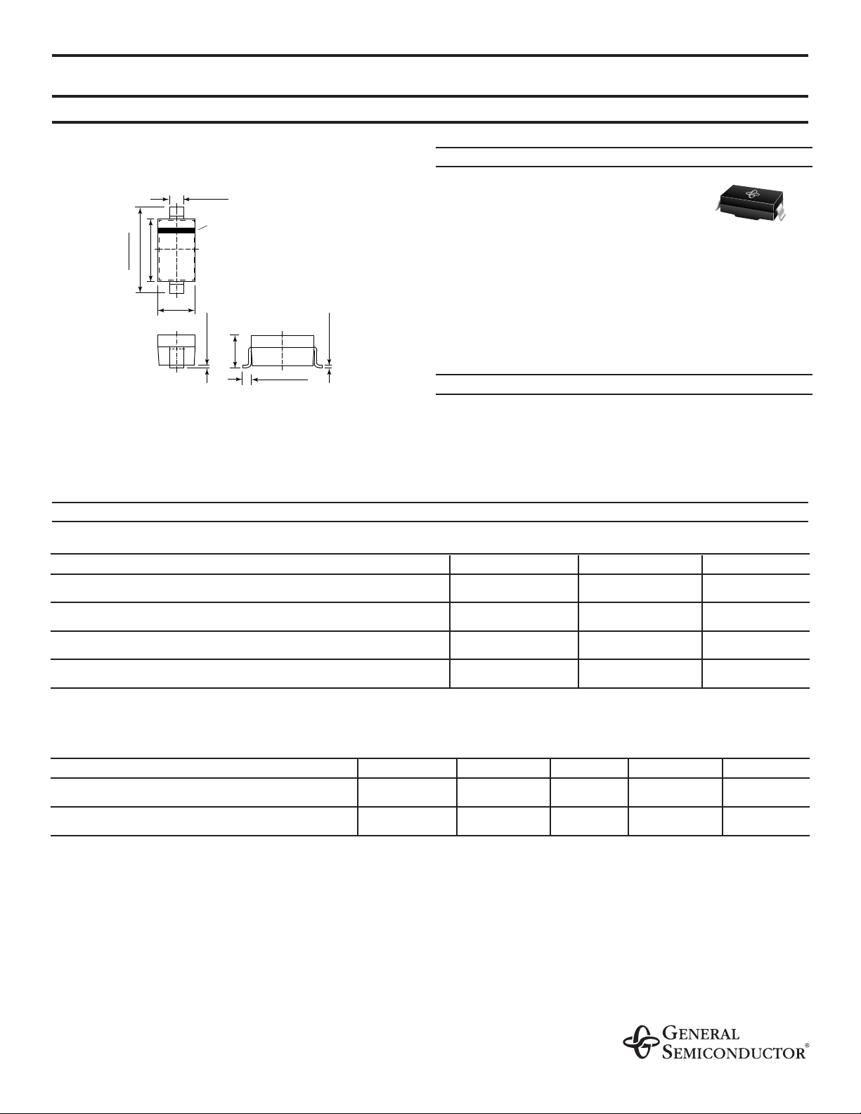
MECHANICAL DATA
Case: SOD-123 Plastic Case
Weight: approx. 0.01 g
Terminals: Solderable per MIL-STD-750, method 2026.
MAXIMUM RATINGS AND ELECTRICAL CHARACTERISTICS
Ratings at 25°C ambient temperature unless otherwise specified.
Dimensions in inches and (millimeters)
SOD-123
1/20/99
ADVANCED INFORMATION
.022 (0.55)
Cathode Mark
.100 (2.55)
.112 (2.85)
.140 (3.55)
.152 (3.85)
.067 (1.70)
.055 (1.40)
Top View
max. .004 (0.1)
max. .053 (1.35)
max. .006 (0.15)
min. .010 (0.25)
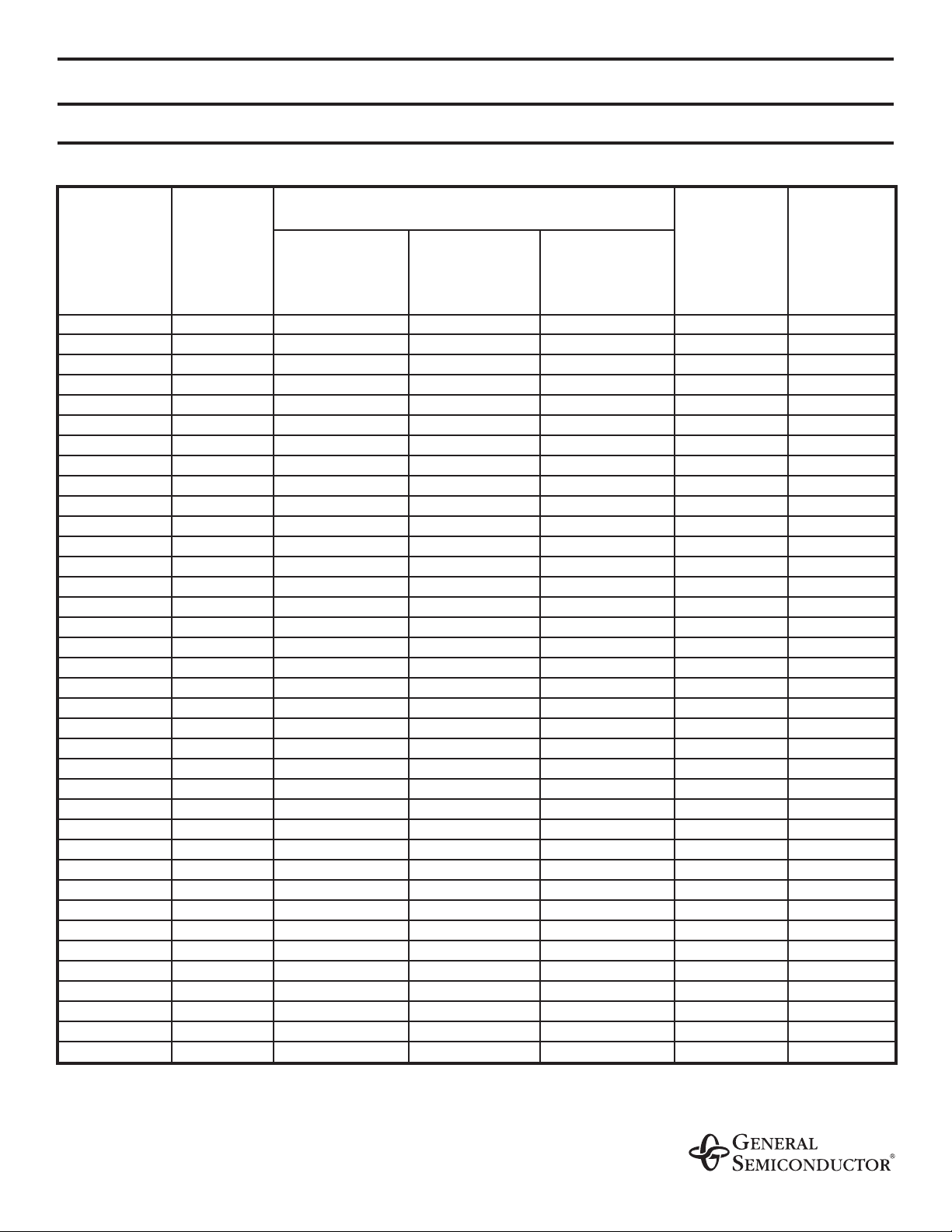
MMSZ4681 CF 2.4 2.28 2.52 2.00 1.0
MMSZ4682 CH 2.7 2.57 2.84 1.00 1.0
MMSZ4683 CJ 3.0 2.85 3.15 0.80 1.0
MMSZ4684 CK 3.3 3.14 3.47 7.50 1.5
MMSZ4685 CM 3.6 3.42 3.78 7.50 2.0
MMSZ4686 CN 3.9 3.71 4.10 5.00 2.0
MMSZ4687 CP 4.3 4.09 4.52 4.00 2.0
MMSZ4688 CT 4.7 4.47 4.94 10.0 3.0
MMSZ4689 CU 5.1 4.85 5.36 10.0 3.0
MMSZ4690 CV 5.6 5.32 5.88 10.0 4.0
MMSZ4691 CA 6.2 5.89 6.51 10.0 5.0
MMSZ4692 CX 6.8 6.46 7.14 10.0 5.1
MMSZ4693 CY 7.5 7.13 7.88 10.0 5.7
MMSZ4694 CZ 8.2 7.79 8.61 1.00 6.2
MMSZ4695 DC 8.7 8.27 9.14 1.00 6.6
MMSZ4696 DD 9.1 8.65 9.56 1.00 6.9
MMSZ4697 DE 10.0 9.50 10.5 1.00 7.6
MMSZ4698 DF 11.0 10.5 11.6 0.05 8.4
MMSZ4699 DH 12.0 11.4 12.6 0.05 9.1
MMSZ4700 DJ 13.0 12.4 13.7 0.05 9.8
MMSZ4701 DK 14.0 13.3 14.7 0.05 10.6
MMSZ4702 DM 15.0 14.3 15.8 0.05 11.4
MMSZ4703 DN 16.0 15.2 16.8 0.05 12.1
MMSZ4704 DP 17.0 16.2 17.9 0.05 12.9
MMSZ4705 DT 18.0 17.1 18.9 0.05 13.6
MMSZ4706 DU 19.0 18.1 20.0 0.05 14.4
MMSZ4707 DV 20.0 19.0 21.0 0.01 15.2
MMSZ4708 DA 22.0 20.9 23.1 0.01 16.7
MMSZ4709 DZ 24.0 22.8 25.2 0.01 18.2
MMSZ4710 DY 25.0 23.8 26.3 0.01 19.0
MMSZ4711 EA 27.0 25.7 28.4 0.01 20.4
MMSZ4712 EC 28.0 26.6 29.4 0.01 21.2
MMSZ4713 ED 30.0 28.5 31.5 0.01 22.8
MMSZ4714 EE 33.0 31.4 34.7 0.01 25.0
MMSZ4715 EF 36.0 34.2 37.8 0.01 27.3
MMSZ4716 EH 39.0 37.1 41.0 0.01 29.6
MMSZ4717 EJ 43.0 40.9 45.2 0.01 32.6
MMSZ4681 THRU MMSZ4717
ELECTRICAL CHARACTERISTICS
Type
Marking
Code
Zener Voltage
(1)
VZ @ I
ZT
=
50µA (Volts)
Test Voltage
V
R
(Volts)
Nominal
NOTES:
(1) Measured with device junction in thermal equilibrium
Min Max
Max Reverse
Current
I
R
(µA)
T
A
= 25°C unless otherwise specified
 Loading...